KR102296805B1 - How to pattern a substrate using layers with multiple materials - Google Patents
How to pattern a substrate using layers with multiple materials Download PDFInfo
- Publication number
- KR102296805B1 KR102296805B1 KR1020187037358A KR20187037358A KR102296805B1 KR 102296805 B1 KR102296805 B1 KR 102296805B1 KR 1020187037358 A KR1020187037358 A KR 1020187037358A KR 20187037358 A KR20187037358 A KR 20187037358A KR 102296805 B1 KR102296805 B1 KR 102296805B1
- Authority
- KR
- South Korea
- Prior art keywords
- substrate
- etch
- mandrel
- layer
- sidewall spacers
- Prior art date
Links
Images


Classifications
-
- H—ELECTRICITY
- H01—ELECTRIC ELEMENTS
- H01L—SEMICONDUCTOR DEVICES NOT COVERED BY CLASS H10
- H01L21/00—Processes or apparatus adapted for the manufacture or treatment of semiconductor or solid state devices or of parts thereof
- H01L21/02—Manufacture or treatment of semiconductor devices or of parts thereof
- H01L21/027—Making masks on semiconductor bodies for further photolithographic processing not provided for in group H01L21/18 or H01L21/34
- H01L21/0271—Making masks on semiconductor bodies for further photolithographic processing not provided for in group H01L21/18 or H01L21/34 comprising organic layers
- H01L21/0273—Making masks on semiconductor bodies for further photolithographic processing not provided for in group H01L21/18 or H01L21/34 comprising organic layers characterised by the treatment of photoresist layers
- H01L21/0274—Photolithographic processes
-
- H—ELECTRICITY
- H01—ELECTRIC ELEMENTS
- H01L—SEMICONDUCTOR DEVICES NOT COVERED BY CLASS H10
- H01L21/00—Processes or apparatus adapted for the manufacture or treatment of semiconductor or solid state devices or of parts thereof
- H01L21/02—Manufacture or treatment of semiconductor devices or of parts thereof
- H01L21/027—Making masks on semiconductor bodies for further photolithographic processing not provided for in group H01L21/18 or H01L21/34
- H01L21/033—Making masks on semiconductor bodies for further photolithographic processing not provided for in group H01L21/18 or H01L21/34 comprising inorganic layers
- H01L21/0334—Making masks on semiconductor bodies for further photolithographic processing not provided for in group H01L21/18 or H01L21/34 comprising inorganic layers characterised by their size, orientation, disposition, behaviour, shape, in horizontal or vertical plane
- H01L21/0338—Process specially adapted to improve the resolution of the mask
-
- H—ELECTRICITY
- H01—ELECTRIC ELEMENTS
- H01L—SEMICONDUCTOR DEVICES NOT COVERED BY CLASS H10
- H01L21/00—Processes or apparatus adapted for the manufacture or treatment of semiconductor or solid state devices or of parts thereof
- H01L21/02—Manufacture or treatment of semiconductor devices or of parts thereof
- H01L21/027—Making masks on semiconductor bodies for further photolithographic processing not provided for in group H01L21/18 or H01L21/34
- H01L21/033—Making masks on semiconductor bodies for further photolithographic processing not provided for in group H01L21/18 or H01L21/34 comprising inorganic layers
- H01L21/0334—Making masks on semiconductor bodies for further photolithographic processing not provided for in group H01L21/18 or H01L21/34 comprising inorganic layers characterised by their size, orientation, disposition, behaviour, shape, in horizontal or vertical plane
- H01L21/0337—Making masks on semiconductor bodies for further photolithographic processing not provided for in group H01L21/18 or H01L21/34 comprising inorganic layers characterised by their size, orientation, disposition, behaviour, shape, in horizontal or vertical plane characterised by the process involved to create the mask, e.g. lift-off masks, sidewalls, or to modify the mask, e.g. pre-treatment, post-treatment
-
- H—ELECTRICITY
- H01—ELECTRIC ELEMENTS
- H01L—SEMICONDUCTOR DEVICES NOT COVERED BY CLASS H10
- H01L21/00—Processes or apparatus adapted for the manufacture or treatment of semiconductor or solid state devices or of parts thereof
- H01L21/02—Manufacture or treatment of semiconductor devices or of parts thereof
- H01L21/027—Making masks on semiconductor bodies for further photolithographic processing not provided for in group H01L21/18 or H01L21/34
- H01L21/033—Making masks on semiconductor bodies for further photolithographic processing not provided for in group H01L21/18 or H01L21/34 comprising inorganic layers
- H01L21/0332—Making masks on semiconductor bodies for further photolithographic processing not provided for in group H01L21/18 or H01L21/34 comprising inorganic layers characterised by their composition, e.g. multilayer masks, materials
-
- H—ELECTRICITY
- H01—ELECTRIC ELEMENTS
- H01L—SEMICONDUCTOR DEVICES NOT COVERED BY CLASS H10
- H01L21/00—Processes or apparatus adapted for the manufacture or treatment of semiconductor or solid state devices or of parts thereof
- H01L21/02—Manufacture or treatment of semiconductor devices or of parts thereof
- H01L21/027—Making masks on semiconductor bodies for further photolithographic processing not provided for in group H01L21/18 or H01L21/34
- H01L21/033—Making masks on semiconductor bodies for further photolithographic processing not provided for in group H01L21/18 or H01L21/34 comprising inorganic layers
- H01L21/0334—Making masks on semiconductor bodies for further photolithographic processing not provided for in group H01L21/18 or H01L21/34 comprising inorganic layers characterised by their size, orientation, disposition, behaviour, shape, in horizontal or vertical plane
- H01L21/0335—Making masks on semiconductor bodies for further photolithographic processing not provided for in group H01L21/18 or H01L21/34 comprising inorganic layers characterised by their size, orientation, disposition, behaviour, shape, in horizontal or vertical plane characterised by their behaviour during the process, e.g. soluble masks, redeposited masks
-
- H—ELECTRICITY
- H01—ELECTRIC ELEMENTS
- H01L—SEMICONDUCTOR DEVICES NOT COVERED BY CLASS H10
- H01L21/00—Processes or apparatus adapted for the manufacture or treatment of semiconductor or solid state devices or of parts thereof
- H01L21/02—Manufacture or treatment of semiconductor devices or of parts thereof
- H01L21/04—Manufacture or treatment of semiconductor devices or of parts thereof the devices having at least one potential-jump barrier or surface barrier, e.g. PN junction, depletion layer or carrier concentration layer
- H01L21/18—Manufacture or treatment of semiconductor devices or of parts thereof the devices having at least one potential-jump barrier or surface barrier, e.g. PN junction, depletion layer or carrier concentration layer the devices having semiconductor bodies comprising elements of Group IV of the Periodic System or AIIIBV compounds with or without impurities, e.g. doping materials
- H01L21/30—Treatment of semiconductor bodies using processes or apparatus not provided for in groups H01L21/20 - H01L21/26
- H01L21/302—Treatment of semiconductor bodies using processes or apparatus not provided for in groups H01L21/20 - H01L21/26 to change their surface-physical characteristics or shape, e.g. etching, polishing, cutting
- H01L21/306—Chemical or electrical treatment, e.g. electrolytic etching
- H01L21/3065—Plasma etching; Reactive-ion etching
-
- H—ELECTRICITY
- H01—ELECTRIC ELEMENTS
- H01L—SEMICONDUCTOR DEVICES NOT COVERED BY CLASS H10
- H01L21/00—Processes or apparatus adapted for the manufacture or treatment of semiconductor or solid state devices or of parts thereof
- H01L21/70—Manufacture or treatment of devices consisting of a plurality of solid state components formed in or on a common substrate or of parts thereof; Manufacture of integrated circuit devices or of parts thereof
- H01L21/71—Manufacture of specific parts of devices defined in group H01L21/70
- H01L21/768—Applying interconnections to be used for carrying current between separate components within a device comprising conductors and dielectrics
- H01L21/76801—Applying interconnections to be used for carrying current between separate components within a device comprising conductors and dielectrics characterised by the formation and the after-treatment of the dielectrics, e.g. smoothing
- H01L21/76802—Applying interconnections to be used for carrying current between separate components within a device comprising conductors and dielectrics characterised by the formation and the after-treatment of the dielectrics, e.g. smoothing by forming openings in dielectrics
- H01L21/76807—Applying interconnections to be used for carrying current between separate components within a device comprising conductors and dielectrics characterised by the formation and the after-treatment of the dielectrics, e.g. smoothing by forming openings in dielectrics for dual damascene structures
- H01L21/76811—Applying interconnections to be used for carrying current between separate components within a device comprising conductors and dielectrics characterised by the formation and the after-treatment of the dielectrics, e.g. smoothing by forming openings in dielectrics for dual damascene structures involving multiple stacked pre-patterned masks
-
- H—ELECTRICITY
- H01—ELECTRIC ELEMENTS
- H01L—SEMICONDUCTOR DEVICES NOT COVERED BY CLASS H10
- H01L21/00—Processes or apparatus adapted for the manufacture or treatment of semiconductor or solid state devices or of parts thereof
- H01L21/70—Manufacture or treatment of devices consisting of a plurality of solid state components formed in or on a common substrate or of parts thereof; Manufacture of integrated circuit devices or of parts thereof
- H01L21/71—Manufacture of specific parts of devices defined in group H01L21/70
- H01L21/768—Applying interconnections to be used for carrying current between separate components within a device comprising conductors and dielectrics
- H01L21/76801—Applying interconnections to be used for carrying current between separate components within a device comprising conductors and dielectrics characterised by the formation and the after-treatment of the dielectrics, e.g. smoothing
- H01L21/76802—Applying interconnections to be used for carrying current between separate components within a device comprising conductors and dielectrics characterised by the formation and the after-treatment of the dielectrics, e.g. smoothing by forming openings in dielectrics
- H01L21/76816—Aspects relating to the layout of the pattern or to the size of vias or trenches
-
- H—ELECTRICITY
- H01—ELECTRIC ELEMENTS
- H01L—SEMICONDUCTOR DEVICES NOT COVERED BY CLASS H10
- H01L21/00—Processes or apparatus adapted for the manufacture or treatment of semiconductor or solid state devices or of parts thereof
- H01L21/70—Manufacture or treatment of devices consisting of a plurality of solid state components formed in or on a common substrate or of parts thereof; Manufacture of integrated circuit devices or of parts thereof
- H01L21/71—Manufacture of specific parts of devices defined in group H01L21/70
- H01L21/768—Applying interconnections to be used for carrying current between separate components within a device comprising conductors and dielectrics
- H01L21/76801—Applying interconnections to be used for carrying current between separate components within a device comprising conductors and dielectrics characterised by the formation and the after-treatment of the dielectrics, e.g. smoothing
- H01L21/76829—Applying interconnections to be used for carrying current between separate components within a device comprising conductors and dielectrics characterised by the formation and the after-treatment of the dielectrics, e.g. smoothing characterised by the formation of thin functional dielectric layers, e.g. dielectric etch-stop, barrier, capping or liner layers
- H01L21/76832—Multiple layers
Abstract
본 명세서의 기술은 에칭을 위해 부식성 가스를 필요로 하지 않고 스택 재료 및 다중 색상 재료를 집적할 수 있게 한다. 이 기술은 층 또는 색상 또는 재료가 모두 실리콘 함유 재료 및 유기 재료로 제한될 수 있는 자기-정렬 패턴 축소를 위한 다중 라인 층을 가능하게 한다. 이러한 기술은 자기-정렬 블록을 위한 모든 비부식성 에칭 호환 스택을 사용하여 5 nm 백-엔드-오브-라인 트렌치 패터닝에 대해 자기-정렬 블록 집적을 가능하게 한다. 실시예는 재료의 유형 및/또는 재료의 높이 및 에칭 레이트에 기초하여 여러 라인 중 하나에 에칭 선택도를 제공하기 위해 동일한 재료이지만 상이한 높이의 라인을 사용하는 것을 포함한다.The techniques herein allow for the integration of stack materials and multi-color materials without the need for corrosive gases to etch. This technique enables multi-line layers for self-aligned pattern reduction where the layer or color or material can be both limited to silicon-containing materials and organic materials. This technique enables self-aligned block integration for 5 nm back-end-of-line trench patterning using any non-corrosive etch compatible stack for self-aligned blocks. Embodiments include using the same material but different height lines to provide etch selectivity to one of several lines based on the type of material and/or the height of the material and the etch rate.
Description
관련 출원의 상초 참조Early reference to related application
본 출원은 2016년 5월 23일자로 출원된 "다중 재료를 갖는 층을 사용하여 기판을 패터닝하는 방법"이라는 명칭의 미국 가출원 제62/340,279호의 이익을 주장하며, 이는 본 명세서에서 그 전체가 참조에 의해 통합된다. This application claims the benefit of US Provisional Application Serial No. 62/340,279, entitled “Method of Patterning a Substrate Using a Layer with Multiple Materials,” filed on May 23, 2016, which is incorporated herein by reference in its entirety. is integrated by
기술 분야technical field
본 개시는 기판 처리에 관한 것으로, 보다 구체적으로는 반도체 웨이퍼를 패터닝하는 것을 포함하는 기판을 패터닝하는 기술에 관한 것이다. The present disclosure relates to substrate processing, and more particularly to techniques for patterning a substrate including patterning a semiconductor wafer.
리소그래피 공정에서 라인 폭을 축소시키는 방법은 역사적으로 보다 큰 NA 광학(개구부수), 보다 짧은 노광 파장, 또는 공기 이외의 계면 매체(예를 들어, 수침)를 사용하는 것과 관련이 있다. 종래의 리소그래피 공정의 해상도가 이론적인 한계에 근접함에 따라, 제조사는 광학 한계를 극복하기 위해 더블 패터닝(double-patterning, DP) 방법으로 전환하기 시작하였다.Methods of reducing line width in lithography processes have historically been associated with using larger NA optics (number of apertures), shorter exposure wavelengths, or interfacial media other than air (eg, water immersion). As the resolution of conventional lithography processes approaches theoretical limits, manufacturers have begun to switch to double-patterning (DP) methods to overcome optical limitations.
재료 처리 방법(예를 들어, 포토리소그래피)에서, 패터닝된 층을 생성하는 것은 포토레지스트와 같은 방사선-민감성(radiation-sensitive) 재료의 박막 층을 기판의 상부 표면에 도포하는 것을 포함한다. 이 방사선-민감성 재료는 릴리프(relief) 패턴으로 변형되며, 릴리프 패턴은 기판 상의 하부 층에 패턴을 전사하기 위해 에칭 마스크로서 사용될 수 있다. 복사서-민감성 재료의 패터닝은 일반적으로 예를 들어 포토리소그래피 시스템을 사용하여 방사선-민감성 재효 상에 레티클(및 관련 광학기)을 통해 화학 방사선을 노광하는 것을 포함한다. 이어서, 이 노광은 현상액을 사용한 방사선-민감성 재료의 조사된 영역(포지티브 포토레지스트의 경우) 또는 조사되지 않은 영역(네거티브 레지스트의 경우)의 제거가 후속될 수 있다. 이 마스크 층은 다중 서브 층을 포함할 수 있다. In a material processing method (eg, photolithography), creating a patterned layer includes applying a thin layer of a radiation-sensitive material, such as a photoresist, to an upper surface of a substrate. This radiation-sensitive material is transformed into a relief pattern, which can be used as an etch mask to transfer the pattern to an underlying layer on the substrate. Patterning of radiation-sensitive materials generally involves exposing actinic radiation through a reticle (and associated optics) onto a radiation-sensitive reproduction using, for example, a photolithography system. This exposure can then be followed by removal of irradiated (for positive photoresist) or unirradiated (for negative resist) areas of the radiation-sensitive material with a developer. This mask layer may include multiple sub-layers.
방사선 또는 광의 패턴을 기판 상에 노광시키기 위한 종래의 리소그래피 기술은 노광된 피처의 크기를 제한하고 노광된 피처 사이의 피치 또는 간격을 제한하는 다양한 도전 과제들을 가진다. 노광 제한을 완화하기 위한 하나의 종래 기술은 더블 패터닝 접근법을 사용하여 종래의 리소그래피 기술로 현재 가능한 것보다 작은 피치에서 더 작은 피처의 패터닝을 가능하게 하는 것이다.Conventional lithographic techniques for exposing patterns of radiation or light onto a substrate have various challenges that limit the size of the exposed features and limit the pitch or spacing between the exposed features. One prior art for relaxing exposure limitations is to use a double patterning approach to enable the patterning of smaller features at smaller pitches than currently possible with conventional lithography techniques.
반도체 기술은 14 nm, 7 nm, 5 nm 이하의 피처 크기를 포함하여 더 작은 피처 크기로 계속해서 진행되고 있다. 다양한 요소가 제조되는 피처의 크기의 지속적으로 감소하면 피처를 형성하는데 사용되는 기술에 대한 요구도 커진다. "피치"의 개념은 이들 피처의 크기 결정을 설명하는데 사용될 수 있다. 피치는 인접한 2개의 반복되는 피처에서 2개의 동일한 지점 사이의 거리이다. 그리고, 하프-피치는 어레이의 동일한 피처 사이의 거리의 절반이다.Semiconductor technology continues to advance into smaller feature sizes, including feature sizes below 14 nm, 7 nm, and 5 nm. As the size of the features from which the various elements are manufactured continues to decrease, so does the demand for the techniques used to form the features. The concept of “pitch” can be used to describe the sizing of these features. Pitch is the distance between two identical points in two adjacent repeating features. And, half-pitch is half the distance between identical features of the array.
"피치 더블링(pitch doubling)" 등에 의해 예시된 바와 같이 종종 다소 잘못되었지만 일상적으로 "피치 멀티플리케이션(pitch multiplication)"이하 용어의 피치 감소 기술은 피처 크기 제한(광학 해상도 제한)을 넘어 포토리소그래피의 능력을 확장시킬 수 있다. 즉, 종래의 특정 인수에 의한 피치의 멀티플리케이션(보다 정확하게 피치 감소 또는 피치 밀도의 멀티플리케이션)은 지정된 인수에 의해 목표 피치를 감소시키는 것을 포함한다. 193 nm 침지 리소그래피로 사용되는 더블 패터닝 기술은 관례적으로 22 nm 노드 이하를 패터닝하는데 가장 유망한 기술 중 하나로 간주됩니다. 주목할 만한 점은 자기-정렬 스페이서 더블 패터닝(self-aligned spacer double patterning; SADP)이 피치 밀도 더블링 공정으로서 이미 확립되었고 NAND 플래시 메모리 디바이스의 대량 제조에서 적용되었다는 것이다. 또한, SADP 단계를 피치 쿼드루플(quadrupling)로서 2회 반복하기 위해 초미세 해상도가 얻어질 수 있다.Although often somewhat erroneously, as exemplified by “pitch doubling” and the like, pitch reduction techniques commonly referred to as “pitch multiplication” or the like, pitch reduction techniques, are the ability of photolithography to go beyond feature size limitations (optical resolution limitations). can be expanded. That is, conventional multiplication of pitch by a specified factor (more precisely, multiplication of pitch reduction or pitch density) involves reducing the target pitch by a specified factor. The double patterning technique used with 193 nm immersion lithography is conventionally regarded as one of the most promising techniques for patterning the 22 nm node and below. It is noteworthy that self-aligned spacer double patterning (SADP) has already been established as a pitch density doubling process and has been applied in mass production of NAND flash memory devices. Also, ultra-fine resolution can be obtained to repeat the SADP step twice as pitch quadrupling.
패턴 밀도 또는 피치 밀도를 증가시키는 몇몇 패터닝 기술이 존재하지만, 종래의 패터닝 기술은 낮은 해상도 또는 에칭된 피처의 거친 표면으로 인해 어려움을 겪는다. 따라서, 종래 기술은 매우 작은 치수(20 nm 이하)에 소망되는 일정 수준의 균일성 및 충실도를 제공할 수 없다. 신뢰성있는 리소그래피 기술은 약 80 nm의 피치를 갖는 피처를 생성할 수 있다. 그러나, 종래 및 새롭게 부상하고 있는 설계 사양은 약 20 nm 또는 10 nm 미만의 임계 치수를 갖는 피처를 제조하고자 한다. 또한, 피치 밀도 더블링 및 쿼드루플 기술과 함께, 하위 해상도 라인이 생성될 수 있지만, 그러한 절단에 필요한 피치 및 치수가 종래의 포토리소그래피 시스템의 능력보다 훨씬 낮기 때문에 이들 라인 사이의 절단 또는 접속은 도전 과제이다. Although several patterning techniques exist to increase pattern density or pitch density, conventional patterning techniques suffer from low resolution or rough surfaces of the etched features. Thus, the prior art cannot provide the desired level of uniformity and fidelity in very small dimensions (20 nm or less). Reliable lithographic techniques can produce features with a pitch of about 80 nm. However, conventional and emerging design specifications seek to fabricate features with critical dimensions of less than about 20 nm or 10 nm. Also, with pitch density doubling and quadruple techniques, sub-resolution lines can be created, but cutting or connecting between these lines is challenging because the pitch and dimensions required for such cutting are much lower than the capabilities of conventional photolithography systems. am.
피치 스케일링을 유지하기 위해, 노드 7 이상의 백-엔드-오브-라인(back-end-of-line, BEOL) 트렌치 패터닝은 36 nm 이하의 피치를 요구한다. 이 작은 피치를 패터닝하는 것은 도전 과제가 될 수 있지만, EUV 13.5 nm 리소그래피 자기-정렬 더블 패터닝(self-aligned double patterning, SADP), 193 nm 자기-정렬 쿼드루플 패터닝(self-aligned quadruple patterning, SAQP) 또는 비아 유도 자기-조립(directed self-assembly, DSA)을 포함한 다양한 방법으로 달성될 수 있다. 트렌치 패터닝 공정의 주요 단계는 무한 라인이 체인 또는 라인 단부 컷 등으로 절단되어 최종 원하는 트렌치 레이아웃을 형성하는 영역 선택 블로킹 공정이다. 피치가 작아짐에 따라이 블록 패턴의 오버레이 요건은 리소그래피 툴의 능력을 넘어서고, 이는 BEOL에서의 계속되는 피치 스케일링을 방지할 수 있다.To maintain pitch scaling, back-end-of-line (BEOL) trench patterning above node 7 requires pitches of 36 nm or less. Patterning this small pitch can be challenging, but EUV 13.5 nm lithographic self-aligned double patterning (SADP), 193 nm self-aligned quadruple patterning (SAQP) Alternatively, via directed self-assembly (DSA) can be achieved in a variety of ways. A key step in the trench patterning process is an area selection blocking process in which endless lines are cut with chains or line end cuts to form the final desired trench layout. As the pitch becomes smaller, the overlay requirements of this block pattern exceed the capabilities of the lithography tool, which may prevent continued pitch scaling in BEOL.
본 명세서에 개시된 기술은 고해상도 피처 생성, 및 또한 하위 해상도 피처의 피치 상의 절단을 위한 피치 감소(피치/피처 밀도 증가)를 위한 방법을 제공한다. 본 명세서의 기술은 에칭을 위해 부식성 가스를 필요로 하지 않고 스택 재료 및 상이한 "색상(color)" 재료를 집적할 수 있게 한다. 실시예는 층 또는 색상 또는 재료(상이한 에칭 저항성)가 모두 실리콘 함유 재료 및 유기 재료로 제한될 수 있다는 것을 포함할 수 있다. 이러한 기술은 자기-정렬 블록을 위한 모든 비부식성 에칭 호환 스택을 사용하여 5 nm 백-엔드-오브-라인 트렌치 패터닝에 대해 자기-정렬 블록 집적을 가능하게 한다. 자기-정렬 블로킹은 직접적인 리소그래피/블록 패턴의 다루기 힘든 오버레이 요건을 제거하고, 리소그래피 과제를 에칭 선택도 과제로 대체한다. 리소그래피 패턴의 개구부를 더욱 좁히거나 줄이기 위해 상이한 색상(상이한 에칭 저항성을 갖는 재료)의 라인을 갖는 다중 라인 층이 사용된다. 본 명세서에서 상이한 색상의 라인은 동일한 재료의 상이한 높이의 라인을 사용하여 달성될 수 있다.The techniques disclosed herein provide a method for high resolution feature creation, and also for pitch reduction (increasing pitch/feature density) for cutting on the pitch of lower resolution features. The techniques herein allow the integration of stack materials and different “color” materials without the need for corrosive gases to etch. Embodiments may include that a layer or color or material (different etch resistance) may be limited to both silicon-containing materials and organic materials. This technique enables self-aligned block integration for 5 nm back-end-of-line trench patterning using any non-corrosive etch compatible stack for self-aligned blocks. Self-aligned blocking eliminates the cumbersome overlay requirements of direct lithography/block patterns and replaces lithography challenges with etch selectivity challenges. Multi-line layers with lines of different colors (materials with different etch resistance) are used to further narrow or reduce the openings in the lithography pattern. Different colored lines herein can be achieved using different height lines of the same material.
물론, 여기서 설명된 바와 같은 상이한 단계들의 논의 순서는 명료함을 위해 제시되었다. 일반적으로, 그러한 단계들은 임의의 적합한 순서로 수행될 수 있다. 추가적으로, 여기에 상이한 피쳐들, 기술들, 구성들 등 각각이 본 발명개시의 다른 장소들에서 논의될수 있지만, 그 개념들 각각은 서로 독립적으로 또는 서로 조합하여 실행될 수 있는 것으로 의도된다. 따라서, 본 발명은 다양한 상이한 방법들로 실시되고 보여질 수 있다. Of course, the order of discussion of the different steps as described herein has been presented for clarity. In general, such steps may be performed in any suitable order. Additionally, although each of the different features, techniques, configurations, etc. herein may be discussed in different places of this disclosure, it is intended that each of the concepts be practiced independently of one another or in combination with one another. Accordingly, the present invention may be practiced and shown in a variety of different ways.
본 [발명의 내용] 섹션은, 본 발명개시 또는 청구되는 발명의 모든 실시예 및/또는 점진적으로 신규의 양상을 특정하지 않는다는 것을 주목한다. 대신에, 본 [발명의 내용]은 상이한 실시예들의 예비 논의, 및 종래의 기술들을 넘는 대응하는 신규의 사항들만을 제공한다. 본 발명 및 실시예의 추가 상세 및/또는 가능한 전망들에 대해서는, 독자는 이하 더 설명되는 바와 같은 본 발명개시의 [발명을 실시하기 위한 구체적인 내용] 및 대응하는 도면들로 안내된다.It is noted that this section does not specify all embodiments and/or progressively novel aspects of the present disclosure or claimed invention. Instead, the present disclosure provides only a preliminary discussion of different embodiments, and corresponding novelties over the prior art. For further details and/or possible prospects of the invention and embodiment, the reader is directed to the Detailed Description and corresponding drawings of the present disclosure as further described below.
본 발명의 다양한 실시예들 및 그에 수반되는 많은 이점들의 보다 완벽한 이해는, 동반되는 도면들과 함께 고려되는 다음의 상세한 설명들을 참조하여 쉽게 명백해질 것이다. 도면은 반드시 축척대로 그려질 필요없이, 대신에 피쳐, 원리 및 개념들을 도시하는 것을 강조한다.
도 1a 내지 도 18a는 본 명세서에 개시된 실시예에 따른 공정 흐름을 도시하는 예시적인 기판 세그먼트의 측단면도이다.
도 1b 내지 도 18b는 본 명세서에 개시된 실시예에 따른 도 1a 내지 도 18a로부터의 대응하는 예시적인 기판 세그먼트의 상면도이다. 점선의 단면선은 대응하는 측단면도의 단면을 나타낸다.
도 19a 내지 도 32a는 본 명세서에 개시된 실시예에 따른 공정 흐름을 도시하는 예시적인 기판 세그먼트의 측단면도이다.
도 19b 내지 도 32b는 본 명세서에 개시된 실시예에 따른 도 19a 내지 도 32a로부터의 대응하는 예시적인 기판 세그먼트의 상면도이다. 점선의 단면선은 대응하는 측단면도의 단면을 나타낸다.
도 33a 내지 도 46a는 본 명세서에 개시된 실시예에 따른 공정 흐름을 도시하는 예시적인 기판 세그먼트의 측단면도이다.
도 33b 내지 도 46b는 본 명세서에 개시된 실시예에 따른 도 33a 내지 도 46a로부터의 대응하는 예시적인 기판 세그먼트의 상면도이다. 점선의 단면선은 대응하는 측단면도의 단면을 나타낸다. BRIEF DESCRIPTION OF THE DRAWINGS A more complete understanding of various embodiments of the present invention and the many advantages attendant thereto will become readily apparent upon reference to the following detailed description taken in conjunction with the accompanying drawings. The drawings are not necessarily drawn to scale, emphasis instead being placed on illustrating features, principles, and concepts.
1A-18A are cross-sectional side views of exemplary substrate segments illustrating process flows in accordance with embodiments disclosed herein.
1B-18B are top views of corresponding exemplary substrate segments from FIGS. 1A-18A in accordance with embodiments disclosed herein. The dotted cross-section line represents the cross-section of the corresponding side cross-sectional view.
19A-32A are cross-sectional side views of exemplary substrate segments illustrating process flows in accordance with embodiments disclosed herein.
19B-32B are top views of corresponding exemplary substrate segments from FIGS. 19A-32A in accordance with embodiments disclosed herein. The dotted cross-section line represents the cross-section of the corresponding side cross-sectional view.
33A-46A are cross-sectional side views of exemplary substrate segments illustrating process flows in accordance with embodiments disclosed herein.
33B-46B are top views of corresponding exemplary substrate segments from FIGS. 33A-46A in accordance with embodiments disclosed herein. The dotted cross-section line represents the cross-section of the corresponding side cross-sectional view.
본 명세서에 개시된 기술은 고해상도 피처 생성, 및 또한 하위 해상도 피처의 피치 상의 절단을 위한 피치 감소(피치/피처 밀도 증가)를 위한 방법을 제공한다. 본 명세서의 기술은 에칭을 위해 부식성 가스를 필요로 하지 않고 스택 재료 및 다중 색상 재료를 집적할 수 있게 한다. 실시예는 층 또는 색상 또는 재료(상이한 에칭 저항성의 재료)가 모두 실리콘 함유 재료 및 유기 재료로 제한될 수 있다는 것을 포함할 수 있다. 이러한 기술은 자기-정렬 블록을 위한 모든 비부식성 에칭 호환 스택을 사용하여 5 nm 백-엔드-오브-라인 트렌치 패터닝에 대해 자기-정렬 블록 집적을 가능하게 한다. 일부 제조 공정의 경우, 부식성 에칭이 결함을 일으킬 수 있기 때문에 부식성 에칭을 제한하는 것이 바람직하다. 에칭을 위한 비부식성 화학물의 예에는 염소, 브롬 또는 요오드를 함유하지 않는 원소 또는 화합물을 포함한다. 자기-정렬 블록은 발명자가 발명한 기술로서, 하위 해상도 패터닝을 실현하기 위해 상이한 재료의 다중 라인을 사용하는 기술을 지칭한다. at-해상도(또는 더 큰) 개구부를 갖는 에칭 마스크가 이러한 다중 라인 층 위 또는 아래에 형성되고, 이어서 재료의 특정 라인 중 하나 이상이 선택적으로 에칭되어 에칭 마스크에 의해 규정된 것을 더욱 좁히거나 수축시킨다. The techniques disclosed herein provide a method for high resolution feature creation, and also for pitch reduction (increasing pitch/feature density) for cutting on the pitch of lower resolution features. The techniques herein allow for the integration of stack materials and multi-color materials without the need for corrosive gases to etch. Embodiments may include that a layer or color or material (materials of different etch resistance) may be limited to both silicon-containing materials and organic materials. This technique enables self-aligned block integration for 5 nm back-end-of-line trench patterning using any non-corrosive etch compatible stack for self-aligned blocks. For some manufacturing processes, it is desirable to limit corrosive etching because it can cause defects. Examples of non-corrosive chemicals for etching include elements or compounds that do not contain chlorine, bromine or iodine. Self-aligning block is a technique invented by the inventor and refers to a technique that uses multiple lines of different materials to realize sub-resolution patterning. An etch mask with at-resolution (or larger) openings is formed above or below this multi-line layer, and then one or more of specific lines of material are selectively etched to further narrow or constrict what is defined by the etch mask. .
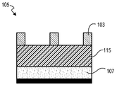
일실시예는 기판을 패터닝하는 방법을 포함한다. 도 1a 내지 18a은 하나의 예시적인 흐름을 도시한다. 이제 도 1a 및 도 1b를 참조하면, 타겟 층(107) 상에 위치된 맨드릴 층(115)을 갖는 기판(105)이 제공된다. 맨드릴 층(115)과 타겟 층(107) 사이에 하나 이상의 막이 위치될 수 있음을 주목한다. 포토레지스트 맨드릴 마스크 또는 에칭 마스크(103)는 맨드릴 층(115)(맨드릴이 형성될 층) 상에 형성된다. 포토레지스트 맨드릴 마스크는 평탄화 층, 반사-방지 코팅 층 등과 같은 임의의 추가 중간 층을 포함 할 수 있으며, 따라서 에칭 마스크(103) 자체는 맨드릴 층(115)과 직접 접촉하지 않을 수 있음을 주목한다. 이들 도면 및 후속 도면에서, 도면 참조에서 "a"를 갖는 도면은 처리되고 있는 예시적인 기판 세그먼트의 측단면도를 도시하고, 도면 참조에서 "b"를 갖는 도면은 대응하는 측단면도가 만들어지는 곳을 나타내기 위한 파선의 절단선을 갖는 동일한 기판 세그먼트의 상면도를 도시한다. 재료 식별의 편의함을 위해, 상면도는 단면을 도시하지 않고 대신에 상단 표면을 도시하지만 단면도와 마찬가지로 재료에 대해 유사한 해칭선을 사용한다.One embodiment includes a method of patterning a substrate. 1A-18A illustrate one exemplary flow. Referring now to FIGS. 1A and 1B , a
에칭 마스크(103)를 사용하여, 맨드릴(110)은 예를 들어 방향성 또는 이방성 에칭을 이용하여 기판의 타겟 층 상에 형성된다. 맨드릴(110)은 제 1 재료로 구성되고, 타겟 층은 제 3 재료로 구성된다. 도 2a 및 도 2b는 예시적인 결과를 도시한다.Using the
이어서, 측벽 스페이서(121)가 맨드릴(110) 상에 형성된다. 측벽 스페이서는 기판(105) 상에 컨포멀 막(120)을 증착함으로써 형성될 수 있다. 도 3a 및 도 3b는 이러한 컨포멀 증착의 예시적인 결과를 도시한다. 이러한 막은 수평 및 수직 표면 모두에 전반적으로 균일한 두께를 가지도록 증착된다는 것이 주목된다. 맨드릴(110)의 상단 표면 위의 컨포멀 막의 부분은, 측벽 스페이서(121)가 맨드릴(110)의 수직 측벽 상에 형성되고 컨포멀 막이 인접한 측벽 스페이서 사이의 타겟 층(107)을 덮도록, 맨드릴(110)의 상단 표면 아래의 컨포멀 막을 남기면서 제거된다. 이 컨포멀 막은 제 2 재료로 구성된다. Then,
컨포멀 막의 상단 표면을 제거하기 위한 다양한 기술이 있다. 하나의 대안으로, 충전 재료(130)가 기판 상에 증착된다. 충전 재료는 컨포멀 막에 의해 규정된 트렌치를 충전하고, 전형적으로 재료의 과잉 퇴적(over burden)을 갖는다. 도 4a 및 도 4b는 예시적인 결과를 도시한다. 그 후, 맨드릴(110)의 상단 표면 위의 컨포멀 막 재료 및 충전 재료(130)를 제거하는 화학 기계적 연마(chemical-mechanical polishing, CMP) 단계가 수행될 수 있다. 도 5a 및 도 5b는 예시적인 결과를 도시한다. 기판은 측벽 스페이서(121)에 의해 규정된 트렌치 내에 충전 재료(130)의 플러그(plug)를 남기면서 맨드릴(110)의 상단 표면까지 평탄화된다는 것을 주목한다.There are various techniques for removing the top surface of a conformal film. In one alternative, a
컨포멀 막의 상단 표면을 제거하기 위한 대체 기술은 에칭 기반이다. 충전 재료(130)의 부분 에칭은 컨포멀 막(120)의 상단 표면이 커버되지 않도록 실행될 수 있다. 예시적인 결과가 도 6a 및 도 6b에 도시된다. 예를 들어, 플라즈마 기반 건식 에칭은 시간 또는 종점(end point) 검출에 기초하여 실행될 수 있다. 또 다른 옵션은 충전 재료(130)가 용해도 이동(solubility shift)이 가능한(현상가능) 경우 충전 재료(130)의 상단부의 확산-제한 용해도 이동을 갖는 습식 에칭이다. 컨포멀 막(120)의 상단 표면이 커버되지 않게 된 후에, 스페이서 개방 에칭이 실행되어 맨드릴(110)의 상단 표면이 커버되지 않게 될 때까지 컨포멀 막을 부분적으로 에칭 할 수 있다. 이것은 맨드릴(110) 상의 측벽 스페이서(121)를 남긴다. 충전 재료(130)의 플러그가 바닥 부분이 에칭되는 것을 방지하기 때문에 컨포멀 막 재료는 여전히 측벽 스페이서(121) 사이의 타겟 층(107)을 커버한다. 예시적인 결과가 도 7a 및 도 7b에 도시된다. 이 스페이서 개방 에칭이 완료한 후에, 도 8a 및 도 8b에 도시된 바와 같이, 남아 있는 충전 재료(130)가 제거될 수 있다. 그 후, 다중 라인 층이 생성되었지만, 스페이서 재료의 일부는 개방되거나 다른 재료로 커버되는 대신에 타겟 층(107)을 커버한다. An alternative technique for removing the top surface of the conformal film is etching based. The partial etching of the filling
이제 도 9a 및 도 9b를 참조하면, 제 1 에칭 마스크(141)가 기판 상에 형성된다. 충전 재료(131)는 평탄화 층으로서 에칭 마스크를 형성하기 전에 기판 상에 증착될 수 있다. 제 1 에칭 마스크(141)는 제 1 재료[맨드릴(110)] 및 제 2 재료[측벽 스페이서(121)] 모두의 영역을 커버하지 않는 개구부를 규정한다. 제 1 재료 및 제 2 재료는 서로에 대해 상이한 에칭 저항성을 가진다. 이것은 하나 이상의 특정 에칭 화학제에 대해 이들 재료 중 하나는 선택적으로 에칭될 수 있고 다른 재료들은 에칭되지 않을 수 있음을 의미하며, 이는 에칭이 발생하지 않거나 또는, 예를 들어 4배 이상 느린 에칭 레이트를 가짐으로써 다른 재료에 비해 현저한 양의 상기 하나의 재료가 에칭됨을 의미한다. 에칭 마스크를 통해 위에서 볼 때 2가지 유형의 재료만 보이지만, 측벽 스페이서와 측벽 스페이서 사이의 컨포멀 막의 높이가 상이하기 때문에, 이 높이 불일치는 에칭 마스크(141)가 에칭 위치 선택을 위한 재료의 3개의 교번하는 라인에 의해 더욱 좁혀질 수 있도록 재료의 3개의 라인을 제공할 수 있지만, 에칭 화학제에 기초한 2가지 유형의 재료만 필요하였다. 이들 2가지 재료 모두는 비부식성 에칭 화학제를 사용하여 에칭 가능하도록 선택될 수 있다.Referring now to FIGS. 9A and 9B , a
기판 상에 에칭 마스크(141)가 위치되면, 예를 들어 방향성 에칭에 의해 충전 재료(131)의 커버되지 않은 부분이 제거될 수 있다. 충전 재료(131)의 이러한 부분을 제거하는 것은 맨드릴(110) 및 측벽 스페이서(121)를 커버되지 않게 한다. 도 10a 및 도 10b는 이 단계 이후의 기판을 도시한다.Once the
측벽 스페이서(121)가 기판 상에 남아 있으면서 인접한 측벽 스페이서(121) 사이의 타겟 층(107)을 커버하는 컨포멀 막이 제거될 때까지 제 2 재료의 커버되지 않은 부분을 선택적으로 에칭하는 제 1 에칭 공정이 실행된다. 예시적인 결과가 도 11a 및 도 11b에 도시된다. 타겟 층(107)의 일부는 이제 위에서 볼 수 있고, 이는 이들 부분이 이제 커버되지 않음을 의미한다. 또한, 이 제 1 에칭 공정은 측벽 스페이서(121)의 높이를 단축시킨다는 것을 주목한다. 그 후, 도 12a 및 도 12b에 도시된 바와 같이, 충전 재료(131) 및 에칭 마스크(141)가 제거될 수 있다.A first etch selectively etching the uncovered portion of the second material until the conformal film covering the
이제 도 13a 및 도 13b를 참조하면, 제 2 에칭 마스크(142)가 기판 상에 형성된다. 충전 재료(132)는 에칭 마스크를 형성하기 전에 기판 상에 증착될 수 있다. 제 2 에칭 마스크(142)는 제 1 재료[맨드릴(110)] 및 제 2 재료[측벽 스페이서(121)] 모두의 영역을 커버하지 않는 개구부를 형성한다. 제 1 재료 및 제 2 재료는 서로에 대해 상이한 에칭 저항성을 가진다.Referring now to FIGS. 13A and 13B , a
에칭 마스크(142)가 기판 상에 위치되면, 예를 들어 방향성 에칭에 의해 충전 재료(132)의 커버되지 않은 부분이 제거될 수 있다. 충전 재료(132)의 이러한 부분을 제거하는 것은 맨드릴(110) 및 측벽 스페이서(121)를 커버되지 않게 한다. 도 14a 및 도 14b는 이 단계 후의 기판을 도시한다. Once the
커버되지 않은 맨드릴(110)이 제거될 때까지 제 1 재료의 커버되지 않은 부분을 선택적으로 에칭하는 제 2 에칭 공정이 실행된다. 예시적인 결과는 도 15a 및 도 15b에 도시된다. 타겟 층(107)의 부분은 이제 위에서 볼 수 있고, 이는 이들 부분이 이제 커버되지 않음을 의미함을 주목한다. 이어서, 충전재(132) 및 에칭 마스크(142)는 도 16a 및 도 16b에 도시된 바와 같이 제거될 수 있다.A second etching process is performed that selectively etches the uncovered portion of the first material until the
맨드릴, 측벽 스페이서, 및 컨포멀 막의 남아 있는 부분은 인접한 측벽 스페이서들 사이의 타겟 층을 커버하여, 타겟 층(107) 또는 다른 기억 층으로 전사하기 위한 에칭 마스크로서 사용될 수 있는 조합된 릴리프 패턴(combined relief pattern)을 함께 형성한다. 도 17a 및 도 17b는 타겟 층(107)의 커버되지 않은 부분을 에칭한 결과를 도시한다. 그 후, 도 18a 및 도 18b는 패턴 전사를 완료한 후에 패터닝된 타겟 층(107)을 도시한다. 따라서, 부식성 에칭없이 형성되는 하위 해상도의 피처가 생성될 수 있다.The mandrel, sidewall spacers, and the remaining portion of the conformal film combine to cover the target layer between adjacent sidewall spacers, which can be used as an etch mask to transfer to the
도 19a 내지 32a 및 도 19b 내지 32b는 다른 예시적인 실시예를 도시한다. 이제 도 19a 및 도 19b를 참조하면, 타겟 층(107) 상에 위치결정된 맨드릴 층(115)을 갖는 기판(105)이 제공된다. 맨드릴 층(115)과 타겟 층(107) 사이에 하나 이상의 막이 위치될 수 있음을 주목한다. 포토레지스트 맨드릴 마스크 또는 에칭 마스크(103)가 맨드릴 층 상에 형성된다. 19A-32A and 19B-32B show another exemplary embodiment. Referring now to FIGS. 19A and 19B , a
그 후, 맨드릴(110)이 기판의 타겟 층(107) 상에 형성된다. 맨드릴은 제 1 재료로 구성되고, 타겟 층은 제 3 재료로 구성된다. 제 1 재료(116)의 막이 맨드릴 사이의 타겟 층을 커버하여 맨드릴(110)의 상단 표면은 제 1 재료의 막의 상단 표면에 비해 더 높다. 이 높이 차이는 제 1 재료(116)의 막 두께의 적어도 2 배이다. 이는 도 20a 및 도 20b에 도시된다. 이러한 맨드릴은 제 1 재료의 층을 통해 완전히 에칭하지 않고 제 1 재료의 층을 통해 부분적으로 에칭함으로써 형성될 수 있다. 이 부분 에칭은 필수적으로 맨드릴(110)을 형성하는 공정의 일부로서 타겟 층 위에 상대적으로 작은 두께의 제 1 재료를 남긴다. A
그 후, 컨포멀 막(120)은 도 21a 및 도 21b에 도시된 바와 같이 기판 상에 증착될 수 있다. 스페이서 개방 에칭은 도 22a 및 도 22b에 도시된 바와 같이 측벽 스페이서(121)를 형성하도록 수행될 수 있다. 측벽 스페이서(121)는 제 2 재료로 구성된다. 측벽 스페이서(121)는 그들 사이에, 제 1 재료(116)의 막이 커버되지 않도록 남겨두는 개방 공간(open space)을 규정한다. Thereafter, the
기판은 충전 재료(131)를 이용하여 평탄화될 수 있고, 그 후 도 23a 및 도 23b에서와 같이 그 위에 제 1 에칭 마스크(141)를 형성할 수 있다. 커버되지 않은 충전 재료(131)는 도 24a 및 도 24b에 도시된 바와 같은 다중 라인 층을 커버하지 않도록 에칭될 수 있다. 이어서, 선택적으로, 제 1 재료(116)의 노출되지 않은 막은 타겟 층(107)이 커버되지 않게 될 때까지 에칭될 수 있다. 커버되지 않은 맨드릴은 또한 제 1 재료의 막과 동일한 양/레이트로 에칭될 것이고, 따라서 이들 커버되지 않은 맨드릴은 높이가 감소될 것이지만 여전히 기판를 커버하기에 충분한 높이를 갖음을 주목한다. 도 25a 및 도 25b는 예시적인 결과를 도시한다. 남아 있는 충전 재료(132) 및 에칭 마스크 재료는 도 26a 및 도 26b에 도시된 바와 같이 제거될 수 있다.The substrate may be planarized using the
기판은 충전 재료(132)를 이용하여 평탄화될 수 있고, 그 후 도 27a 및 도 27b에서와 같이 그 위에 제 2 에칭 마스크(142)를 형성할 수 있다. 커버되지 않은 충전 재료(132)는 도 28a 및 도 28b에 도시된 바와 같이 다중 라인 층을 커버하지 않도록 에칭될 수 있다. 이어서, 선택적으로, 커버되지 않은 맨드릴(110)은 타겟 층(107)이 커버되지 않게 될 때까지 에칭될 수 있다. 도 29a 및 도 29b는 예시적인 결과를 도시한다. 남아 있는 충전 재료(132) 및 에칭 마스크 재료는 도 30a 및 도 30b에 도시된 바와 같이 제거될 수 있다.The substrate may be planarized using the
맨드릴, 측벽 스페이서, 및 제 1 재료의 막의 남아 있는 부분은 타겟 층(107) 또는 다른 기억 층으로 전사하기 위한 에칭 마스크로서 사용될 수 있는 조합된 릴리프 패턴을 함께 형성한다. 도 31a 및 도 31b는 타겟 층(107)의 커버되지 않은 부분을 에칭한 결과를 도시한다. 그 후, 도 32a 및 도 32b는 패턴 전사를 완료한 후에 패터닝된 타겟 층(107)을 도시한다. The mandrel, sidewall spacers, and the remaining portion of the film of first material together form a combined relief pattern that can be used as an etch mask for transfer to the
도 33a 내지 46a 및 도 33b 내지 도 46b는 또 다른 예시적인 실시예를 도시한다. 이제 도 33a 및 도 33b를 참조하면, 타겟 층(107) 상에 위치결정된 맨드릴 층(115)을 갖는 기판(105)이 제공된다. 포토레지스트 맨드릴 마스크 또는 에칭 마스크(103)가 맨드릴 층 상에 형성된다. 맨드릴 층(115)은 타겟 층(107) 상에 삼중층 스택으로서 형성될 수 있다. 삼중층 스택은 하부 층(111), 중간 층(112) 및 상부 층(113)을 포함하며, 각 층은 수평 및 동질(homogeneous)의 층으로서 증착된다. 상부 층(113)은 제 1 재료로 구성되고, 중간 층(112)은 제 5 재료로 구성되고, 하부 층(111)은 제 6 재료로 구성되며, 타겟 층(107)은 제 3 재료로 구성된다. 33A-46A and 33B-46B show another exemplary embodiment. Referring now to FIGS. 33A and 33B , a
그 후, 맨드릴(110)은 제 1 재료로 구성되고, 에칭 마스크(103)를 사용하여 중간 층(112)이 커버되지 않게 될 때까지 상부 층(113)에 맨드릴 패턴을 에칭하는 제 1 에칭을 실행함으로써 기판의 타겟 층(107) 상에 형성된다. 중간 층은 상부 층에 비해 상이한 에칭 저항성을 가져서 중간 층이 맨드릴을 형성하기 위한 에칭 공정을 위한 에칭 정지 층을 제공하도록 한다. 도 34a 및 도 34b는 예시적인 결과를 도시한다. Thereafter, the
그 후, 컨포멀 막(120)은 도 35a 및 도 35b에 도시된 바와 같이 기판 상에 증착될 수 있다. 스페이서 개방 에칭은 스페이서 도 36a 및 도 36b에 도시된 바와 같이 측벽 스페이서(121)를 형성하도록 수행될 수 있다. 측벽 스페이서(121)는 제 2 재료로 구성된다. 측벽 스페이서는 그들 사이에, 하부 층(111)이 커버되지 않도록 남겨두는 개방 공간을 규정한다. 각 컨포멀 막(120) 및 중간 층(112)에 상이한 에칭 화학제가 사용될 수 있다. 대안적으로, 컨포멀 막(120) 및 중간 층(112)은 동일한 재료일 수 있거나 동일한 에칭 화학제를 사용하여 두 재료 모두를 에칭할 수있는 동일한 에칭 저항성을 가질 수 있다. Thereafter, the
기판은 충전 재료(131)를 이용하여 평탄화될 수 있고, 그 후 도 37a 및 도 37b에서와 같이 그 위에 제 1 에칭 마스크(141)를 형성할 수 있다. 커버되지 않은 충전 재료(131)는 도 38a 및도 38b에 도시된 바와 같이 다중 라인 층을 커버하지 않도록 에칭될 수 있다. 이어서, 선택적으로, 하부 층(111)의 커버되지 않은 부분은, 측벽 스페이서가 기판 상에 남아 있으면서 인접한 측벽 스페이서 사이의 타겟 층을 덮는 하부 층(111)이 제거될 때까지 에칭될 수 있다. 그 결과는 도 39a 및 도 39b에 도시된다. 두 재료가 동일한 에칭 저항성을 갖는 경우, 커버되지 않은 맨드릴은 또한 하부 층과 동일한 양으로 에칭될 수 있다. 남아 있는 충전 재료(132) 및 에칭 마스크 재료는 도 40a 및 도 40b에 도시된 바와 같이 제거될 수 있다.The substrate may be planarized using the
기판은 충전 재료(132)를 이용하여 평탄화될 수 있고, 그 후 도 41a 및 도 41b에서와 같이 그 위에 제 2 에칭 마스크(142)를 형성할 수 있다. 커버되지 않은 충전 재료(132)는 도 42a 및 도 42b에 도시된 바와 같이 다중 라인 층을 커버하지 않도록 에칭될 수 있다. 이어서, 선택적으로, 커버되지 않은 맨드릴(110)은 중간 층(112)이 커버되지 않게 될 때까지 에칭될 수 있고, 그 후 중간 층의 커버되지 않은 부분을 에칭하고, 그 후 타겟 층(107)이 커버되지 않게 될 때까지 하부 층(111)의 커버되지 않은 부분을 에칭할 수 있다. 도 43a 및 도 43b는 예시적인 결과를 도시한다. 남아 있는 충전 재료(132) 및 에칭 마스크 재료는 도 44a 및 도 44b에 도시된 바와 같이 제거될 수 있다.The substrate may be planarized using the
맨드릴, 측벽 스페이서, 및 제 1 재료의 막의 남아 있는 부분은 타겟 층(107) 또는 다른 기억 층으로 전사하기 위한 에칭 마스크로서 사용될 수 있는 조합된 릴리프 패턴을 함께 형성한다. 도 45a 및 도 45b는 타겟 층(107)의 커버되지 않은 부분을 에칭한 결과를 도시한다. 도 46a 및 46b는 패턴 전사를 완료한 후에 패터닝된 타겟 층(107)을 도시한다. The mandrel, sidewall spacers, and the remaining portion of the film of first material together form a combined relief pattern that can be used as an etch mask for transfer to the
앞선 설명에서, 본 명세서에서 사용되는 다양한 컴포넌트 및 공정의 설명 및 처리 시스템의 특정 지오메트리와 같은 특정 상세가 열거되었다. 그러나, 여기에 기재된 기술들은 그러한 특정 상세로부터 출발한 다른 실시예들에서 실시될 수 있고, 그러한 상세들은 설명을 위한 것이고 제한을 위한 것이 아님을 이해해야 한다. 여기에 개시된 실시예들은 첨부하는 도면을 참조하여 설명되었다. 마찬가지로, 설명을 위해서, 특정 번호, 재료, 및 구성이 완전한 이해를 제공하기 위해 기재되었다. 그렇기는 하지만, 그러한 특정 상세없이 실시예들이 실시될 수 있다. 실질적으로 동일한 기능의 구조를 갖는 컴포넌트는 동일한 참조 문자에 의해 지정되므로, 임의의 중복 설명은 생략될 수 있다.In the preceding description, specific details have been set forth, such as specific geometries of processing systems and descriptions of various components and processes used herein. However, it is to be understood that the techniques described herein may be practiced in other embodiments departing from those specific details, and that such details are illustrative and not limiting. Embodiments disclosed herein have been described with reference to the accompanying drawings. Likewise, for purposes of explanation, specific numbers, materials, and configurations have been set forth in order to provide a thorough understanding. Even so, embodiments may be practiced without such specific details. Components having substantially the same functional structure are designated by the same reference characters, and thus any redundant description may be omitted.
다양한 실시예들의 이해를 돕기 위해 다수의 개별 동작들로서 설명되었다. 본 설명의 순서는 이러한 동작들이 반드시 순서 의존적임을 나타내는 것이라고 해석되어서는 안된다. 사실, 이러한 동작들은 제시된 순서로 수행될 필요는 없다. 설명된 동작들은 설명된 실시예들과 상이한 순서로 수행될 수 있다. 다양한 추가 동작들이 수행될 수 있고, 그리고/또는 설명된 동작들이 추가의 실시예들에서 생략될 수 있다.To facilitate understanding of various embodiments, a number of separate operations have been described. The order of the description should not be construed as indicating that these operations are necessarily order dependent. In fact, these operations need not be performed in the order presented. The described operations may be performed in a different order than the described embodiments. Various additional operations may be performed, and/or operations described may be omitted in further embodiments.
여기서 사용된 바와 같은 "기판" 또는 "타겟 기판"은 일반적으로 본 발명에 따라 처리되고 있는 대상을 말한다. 기판은 디바이스, 구체적으로는 반도체 또는 달느 전자 디바이스의 임의의 재료 부분 또는 구조물을 포함할 수 있고, 예를 들어, 반도체 웨이퍼, 레티클과 같은 베이스 기판 구조물, 또는 박막과 같은 베이스 기판 구조물 상의 또는 위에 놓인 층일 수 있다. 그러므로, 기판은 패터닝된 또는 패터닝되지 않은, 임의의 특정 베이스 구조물, 아래놓인 층 또는 위에 놓인 층에 한정되지 않고, 오히려 임의의 그러한 층 또는 베이스 구조물, 및 임의의 층들 및/또는 베이스 구조물들의 조합을 포함하도록 고려된다. 본 설명은 특정 유형의 기판을 참조할 수 있지만, 그것은 예시의 목적이다. "Substrate" or "target substrate" as used herein generally refers to the object being processed in accordance with the present invention. The substrate may comprise any material part or structure of a device, specifically a semiconductor or other electronic device, and may be on or overlying a base substrate structure such as, for example, a semiconductor wafer, a base substrate structure such as a reticle, or a thin film. can be layered. Therefore, the substrate is not limited to any particular base structure, underlying layer or overlying layer, patterned or unpatterned, but rather can be any such layer or base structure, and any combination of layers and/or base structures. considered to be included. Although this description may refer to specific types of substrates, it is for purposes of illustration.
당업자는 본 발명과 동일한 목적을 여전히 성취하면서 상기 설명된 기술의 동작들을 여러 변형이 있을 수 있다는 것을 또한 이해할 것이다. 그러한 변형은 본 발명개시의 범위에 의해 커버되도록 의도된다. 그와 같이, 본 발명의실시예들의 상기 설명은 제한을 의도하지 않는다. 그보다는, 본 발명의 실시예에 대한 어떠한 제한은 다음의 청구범위에 제시된다.It will also be understood by those skilled in the art that various modifications may be made to the operations of the techniques described above while still achieving the same objects as the present invention. Such variations are intended to be covered by the scope of the present disclosure. As such, the above description of embodiments of the present invention is not intended to be limiting. Rather, any limitations on the embodiments of the invention are set forth in the claims that follow.
Claims (16)
기판의 타겟 층 상에 맨드릴(mandrel)을 형성하는 단계 - 상기 맨드릴은 제 1 재료로 구성되고, 상기 타겟 층은 제 3 재료로 구성됨 -;
상기 기판 상에 컨포멀(conformal) 막을 증착하고, 측벽 스페이서가 상기 맨드릴의 수직 측벽 상에 형성되고 상기 컨포멀 막이 인접한 측벽 스페이서 사이의 상기 타겟 층을 커버하도록, 상기 맨드릴의 상단 표면 아래의 상기 컨포멀 막을 남기면서 상기 맨드릴의 상단 표면 위의 상기 컨포멀 막의 부분을 제거함으로써, 상기 맨드릴의 측벽 상에 상기 측벽 스페이서를 형성하는 단계 - 상기 컨포멀 막은 제 2 재료로 구성됨 - ;
상기 기판 상에 제 1 에칭 마스크를 형성하는 단계 - 상기 제 1 에칭 마스크는 상기 제 1 재료 및 상기 제 2 재료 모두의 영역을 커버하지 않는 개구부를 규정함 - ;
상기 기판 상에 상기 측벽 스페이서가 남아 있으면서 인접한 측벽 스페이서 사이의 상기 타겟 층을 커버하는 상기 컨포멀 막이 제거될 때까지 상기 제 2 재료의 커버되지 않은 부분을 선택적으로 에칭하는 제 1 에칭 공정을 실행하는 단계;
상기 기판 상에 제 2 에칭 마스크를 형성하는 단계 - 상기 제 2 에칭 마스크는 상기 제 1 재료 및 상기 제 2 재료 모두의 영역을 커버하지 않는 개구부를 규정함 - ; 및
커버되지 않은 맨드릴이 제거될 때까지 상기 제 1 재료의 커버되지 않은 부분을 선택적으로 에칭하는 제 2 에칭 공정을 실행하는 단계
를 더 포함하는, 기판을 패터닝하는 방법.A method for patterning a substrate, comprising:
forming a mandrel on a target layer of a substrate, wherein the mandrel is comprised of a first material and the target layer is comprised of a third material;
depositing a conformal film on the substrate, the conformal film below the top surface of the mandrel, such that sidewall spacers are formed on vertical sidewalls of the mandrel and the conformal film covers the target layer between adjacent sidewall spacers forming the sidewall spacer on a sidewall of the mandrel by removing a portion of the conformal film above a top surface of the mandrel, the conformal film being comprised of a second material, leaving a formal film;
forming a first etch mask on the substrate, the first etch mask defining an opening that does not cover an area of both the first material and the second material;
performing a first etch process selectively etching an uncovered portion of the second material until the conformal film covering the target layer between adjacent sidewall spacers is removed while the sidewall spacers remain on the substrate step;
forming a second etch mask on the substrate, the second etch mask defining an opening that does not cover an area of both the first material and the second material; and
performing a second etching process that selectively etches the uncovered portion of the first material until the uncovered mandrel is removed;
A method of patterning a substrate, further comprising a.
상기 측벽 스페이서를 형성하는 단계는,
상기 컨포멀 막에 의해 규정된 트렌치를 충전하는 제 2 충전 재료를 상기 기판 상에 증착하는 단계; 및
상기 맨드릴의 상단 표면 위의 컨포멀 막 재료 및 제 2 충전 재료를 제거하는 화학 기계적 연마 단계를 실행하는 단계를 포함하는 것인, 기판을 패터닝하는 방법. The method of claim 1,
Forming the sidewall spacer comprises:
depositing on the substrate a second fill material filling the trench defined by the conformal film; and
and performing a chemical mechanical polishing step to remove the conformal film material and the second fill material over the top surface of the mandrel.
상기 컨포멀 막에 의해 규정된 상기 트렌치로부터 상기 제 2 충전 재료를 제거하는 단계
를 더 포함하는, 기판을 패터닝하는 방법. 3. The method of claim 2,
removing the second fill material from the trench defined by the conformal film;
A method of patterning a substrate, further comprising a.
상기 측벽 스페이서를 형성하는 단계는,
상기 컨포멀 막에 의해 규정된 트렌치를 충전하는 제 2 충전 재료를 상기 기판 상에 증착하는 단계;
상기 컨포멀 막의 상단 표면이 커버되지 않게 될 때까지 상기 제 2 충전 재료를 에칭하는 제 3 에칭 공정을 실행하는 단계; 및
상기 맨드릴의 상단 표면이 커버되지 않게 될 때까지 상기 컨포멀 막을 에칭하는 제 4 에칭 공정을 실행하는 단계를 포함하는 것인, 기판을 패터닝하는 방법. The method of claim 1,
Forming the sidewall spacer comprises:
depositing on the substrate a second fill material filling the trench defined by the conformal film;
performing a third etching process that etches the second fill material until the top surface of the conformal film is uncovered; and
and performing a fourth etch process to etch the conformal film until the top surface of the mandrel is uncovered.
상기 기판으로부터 상기 제 2 충전 재료를 제거하는 단계
를 더 포함하는, 기판을 패터닝하는 방법. 5. The method of claim 4,
removing the second fill material from the substrate;
A method of patterning a substrate, further comprising a.
상기 제 1 에칭 공정을 실행한 후 및 상기 제 2 에칭 마스크를 형성하기 전에 상기 제 1 에칭 마스크를 제거하는 단계; 및
상기 제 2 에칭 공정을 실행한 후에, 상기 제 2 에칭 마스크를 제거하는 단계 - 상기 맨드릴, 상기 측벽 스페이서, 및 상기 컨포멀 막의 남아 있는 부분은 인접한 측벽 스페이서 사이의 상기 타겟 층을 커버하여 조합된 릴리프 패턴(combined relief pattern)을 함께 형성함 -
를 더 포함하는, 기판을 패터닝하는 방법. The method of claim 1,
removing the first etch mask after performing the first etch process and before forming the second etch mask; and
after performing the second etch process, removing the second etch mask, wherein the remaining portions of the mandrel, the sidewall spacers, and the conformal film cover the target layer between adjacent sidewall spacers to provide a combined relief Together they form a combined relief pattern -
A method of patterning a substrate, further comprising a.
상기 조합된 릴리프 패턴을 에칭 마스크로서 사용하여 대응하는 패턴을 상기 타겟 층으로 전사하는 제 5 에칭 공정을 실행하는 단계
를 더 포함하는, 기판을 패터닝하는 방법. 7. The method of claim 6,
performing a fifth etch process to transfer a corresponding pattern to the target layer using the combined relief pattern as an etch mask;
A method of patterning a substrate, further comprising a.
상기 제 1 에칭 마스크를 형성하는 단계는, 상기 기판을 평탄화하는 제 1 충전 재료를 상기 기판 상에 증착하는 단계를 포함하고, 상기 제 1 에칭 마스크는 상기 제 1 충전 재료 상에 형성되고, 상기 제 1 충전 재료는 제 4 재료로 구성되고, 상기 제 1 에칭 공정 동안에, 상기 제 1 재료, 상기 제 2 재료, 상기 제 3 재료, 및 상기 제 4 재료는, 상기 제 1 재료로 형성된 상기 맨드릴이 에칭되지 않고, 상기 제 2 재료로 형성된 상기 측벽 스페이서의 높이가 감소되고, 상기 제 3 재료로 형성된 상기 타겟 층의 노출된 부분이 에칭되지 않고, 상기 제 4 재료로 형성된 상기 제 1 충전 재료의 커버되지 않은 부분이 제거되도록, 서로에 대해 상이한 에칭 저항성을 나타내는 것인, 기판을 패터닝하는 방법. The method of claim 1,
Forming the first etch mask includes depositing on the substrate a first fill material for planarizing the substrate, the first etch mask is formed on the first fill material, and A first fill material is comprised of a fourth material, and during the first etching process, the first material, the second material, the third material, and the fourth material are etched by the mandrel formed of the first material. and the height of the sidewall spacers formed of the second material is reduced, the exposed portion of the target layer formed of the third material is not etched, and the first fill material formed of the fourth material is not covered. and exhibit different etch resistances with respect to each other, such that portions that are not are removed.
상기 제 2 에칭 마스크를 형성하는 단계는, 상기 기판을 평탄화하는 제 2 충전 재료를 상기 기판 상에 증착하는 단계를 포함하고, 상기 제 2 에칭 마스크는 상기 제 2 충전 재료 상에 형성되고, 상기 제 2 충전 재료는 제 4 재료로 구성되고, 상기 제 2 에칭 공정 동안에, 상기 제 1 재료, 상기 제 2 재료, 상기 제 3 재료, 및 상기 제 4 재료는, 상기 제 1 재료로 형성된 상기 맨드릴이 제거되고, 상기 제 2 재료로 형성된 상기 측벽 스페이서가 에칭되지 않고, 상기 제 3 재료로 형성된 상기 타겟 층의 노출된 부분이 에칭되지 않고, 상기 제 4 재료로 형성된 상기 제 2 충전 재료의 커버되지 않은 부분이 제거되지 않도록, 서로에 대해 상이한 에칭 저항성을 나타내는 것인, 기판을 패터닝하는 방법.According to claim 1,
Forming the second etch mask includes depositing on the substrate a second fill material for planarizing the substrate, the second etch mask is formed on the second fill material, and The second filling material is comprised of a fourth material, and during the second etching process, the first material, the second material, the third material, and the fourth material are removed by the mandrel formed of the first material. wherein the sidewall spacers formed of the second material are not etched, the exposed portions of the target layer formed of the third material are not etched, and the uncovered portions of the second fill material formed of the fourth material are not etched. and exhibit different etch resistances with respect to each other, such that they are not removed.
제 1 에칭 마스크를 사용하여 기판의 타겟 층 상에 맨드릴을 형성하는 단계 - 상기 맨드릴은 제 1 재료로 구성되고, 상기 타겟 층은 제 3 재료로 구성되며, 상기 제 1 재료의 막이 상기 맨드릴 사이의 상기 타겟 층을 커버하여 상기 맨드릴의 상단 표면이 상기 제 1 재료의 막의 상단 표면에 비해 더 높게 됨 - ;
상기 맨드릴의 측벽 상에 측벽 스페이서를 형성하는 단계 - 상기 측벽 스페이서는 제 2 재료로 구성되고, 상기 측벽 스페이서는 상기 제 1 재료의 막이 커버되지 않도록 남겨두는 개방 공간(open space)을 상기 측벽 스페이서 사이에 규정함 - ;
상기 측벽 스페이서 사이에 규정된 상기 개방 공간을 적어도 부분적으로 충전하는 충전 재료를 상기 기판 상에 증착하는 단계 - 상기 충전 재료는 제 4 재료로 구성되고, 상기 제 1 재료, 상기 제 3 재료, 및 상기 제 4 재료는 모두 화학적으로 서로 상이함 - ;
상기 기판 상에 제 2 에칭 마스크를 형성하는 단계 - 상기 제 2 에칭 마스크는 상기 맨드릴의 상단 층의 부분을 커버하지 않는 개구부를 규정함 - ;
상기 제 2 에칭 마스크를 형성한 후에, 상기 제 2 에칭 마스크를 사용하여, 상기 충전 재료의 커버되지 않은 부분을 에칭하고 상기 맨드릴의 상단 층의 커버되지 않은 부분을 에칭하는 제 1 에칭 공정을 실행하는 단계;
상기 제 1 에칭 공정을 실행한 후에, 상기 기판 상에 제 3 에칭 마스크를 형성하는 단계 - 상기 제 3 에칭 마스크는 상기 제 1 재료 및 상기 제 2 재료 모두의 영역을 커버하지 않는 개구부를 규정함 - ; 및
상기 제 3 에칭 마스크를 사용하여, 커버되지 않은 맨드릴이 제거될 때까지 상기 제 1 재료의 커버되지 않은 부분을 선택적으로 에칭하는 제 2 에칭 공정을 실행하는 단계
를 포함하는, 기판을 패터닝하는 방법.A method for patterning a substrate, comprising:
forming a mandrel on a target layer of a substrate using a first etch mask, wherein the mandrel is comprised of a first material, the target layer is comprised of a third material, and a film of the first material is formed between the mandrels. covering the target layer such that a top surface of the mandrel is higher than a top surface of the film of the first material;
forming sidewall spacers on the sidewalls of the mandrel, the sidewall spacers being comprised of a second material, the sidewall spacers leaving an open space between the sidewall spacers leaving the film of the first material uncovered - stipulated in ;
depositing on the substrate a fill material at least partially filling the open space defined between the sidewall spacers, the fill material being comprised of a fourth material, the first material, the third material, and the The fourth materials are all chemically different from each other;
forming a second etch mask on the substrate, the second etch mask defining an opening that does not cover a portion of the top layer of the mandrel;
after forming the second etch mask, using the second etch mask to perform a first etch process that etches the uncovered portion of the fill material and etches the uncovered portion of the top layer of the mandrel step;
after performing the first etch process, forming a third etch mask on the substrate, the third etch mask defining an opening that does not cover an area of both the first material and the second material; ; and
performing, using the third etch mask, a second etch process that selectively etches the uncovered portion of the first material until the uncovered mandrel is removed;
A method of patterning a substrate comprising:
타겟 층 상에 삼중층(tri-layer) 스택을 형성하는 단계 - 상기 삼중층 스택은 하부 층, 중간 층 및 상부 층을 포함하며, 각 층은 수평 및 동질(homogeneous)의 층으로서 증착되며, 상기 상부 층은 제 1 재료로 구성되고, 상기 중간 층은 제 5 재료로 구성되고, 상기 하부 층은 제 6 재료로 구성되고, 상기 타겟 층은 제 3 재료로 구성됨 - ;
제 1 에칭 마스크를 사용하여 상기 중간 층이 커버되지 않게 될 때까지 상기 상부 층에 맨드릴 패턴을 에칭하는 제 1 에칭 공정을 실행함으로써 상기 제 1 재료로 구성된 맨드릴을 형성하는 단계 - 상기 중간 층은 상기 상부 층에 비해 상이한 에칭 저항성을 가져서 상기 중간 층이 상기 제 1 에칭 공정을 위한 에칭 정지 층을 제공하도록 함 - ;
상기 맨드릴의 측벽 상에 측벽 스페이서를 형성하는 단계 - 상기 측벽 스페이서는 제 2 재료로 구성되고, 상기 측벽 스페이서는 상기 하부 층이 커버되지 않도록 남겨두는 개방 공간을 상기 측벽 스페이서 사이에 규정함 - ;
상기 기판 상에 제 2 에칭 마스크를 형성하는 단계 - 상기 제 2 에칭 마스크는 상기 제 1 재료 및 상기 제 2 재료 모두의 영역을 커버하지 않는 개구부를 규정함 - ;
상기 제 2 에칭 마스크를 사용하여, 상기 기판 상에 상기 측벽 스페이서가 남아 있으면서 인접한 측벽 스페이서 사이의 상기 타겟 층을 커버하는 상기 하부 층이 제거될 때까지 상기 제 6 재료의 커버되지 않은 부분을 선택적으로 에칭하는 제 2 에칭 공정을 실행하는 단계;
상기 제 2 에칭 공정을 실행한 후에, 상기 기판 상에 제 3 에칭 마스크를 형성하는 단계 - 상기 제 3 에칭 마스크는 상기 제 1 재료 및 상기 제 2 재료 모두의 영역을 커버하지 않는 개구부를 규정함 - ; 및
상기 제 3 에칭 마스크를 사용하여, 상기 중간 층이 커버되지 않게 될 때까지 상기 맨드릴의 커버되지 않은 부분을 선택적으로 에칭하는 제 3 에칭 공정을 실행하는 단계
를 포함하는, 기판을 패터닝하는 방법.A method for patterning a substrate, comprising:
forming a tri-layer stack on a target layer, the tri-layer stack comprising a bottom layer, a middle layer and a top layer, each layer deposited as a horizontal and homogeneous layer, wherein the top layer consists of a first material, the middle layer consists of a fifth material, the lower layer consists of a sixth material, and the target layer consists of a third material;
forming a mandrel comprised of the first material by performing a first etch process using a first etch mask to etch a mandrel pattern in the top layer until the intermediate layer is uncovered; having a different etch resistance compared to the top layer such that the middle layer provides an etch stop layer for the first etch process;
forming sidewall spacers on the sidewalls of the mandrel, the sidewall spacers being comprised of a second material, the sidewall spacers defining an open space between the sidewall spacers leaving the underlying layer uncovered;
forming a second etch mask on the substrate, the second etch mask defining an opening that does not cover an area of both the first material and the second material;
Using the second etch mask, the uncovered portions of the sixth material are selectively removed until the underlying layer covering the target layer between adjacent sidewall spacers is removed, leaving the sidewall spacers on the substrate. performing a second etching process to etch;
after performing the second etching process, forming a third etching mask on the substrate, the third etching mask defining an opening that does not cover an area of both the first material and the second material; ; and
performing a third etch process using the third etch mask to selectively etch the uncovered portion of the mandrel until the intermediate layer becomes uncovered;
A method of patterning a substrate comprising:
상기 제 3 에칭 공정을 실행하는 단계는, 상기 맨드릴의 커버되지 않은 부분이 선택적으로 에칭된 후에, 이어서 상기 중간 층의 커버되지 않은 부분을 에칭하는 단계, 및 이어서 상기 타겟 층이 커버되지 않게 될 때까지 상기 하부 층의 커버되지 않은 부분을 에칭하는 단계를 더 포함하고, 상기 제 1 재료와 상기 제 2 재료는 상이한 에칭 저항성을 나타내는 것인, 기판을 패터닝하는 방법.12. The method of claim 11,
Performing the third etching process may include, after the uncovered portion of the mandrel is selectively etched, then etching the uncovered portion of the intermediate layer, and then when the target layer becomes uncovered. and etching the uncovered portion of the underlying layer until the first material and the second material exhibit different etch resistances.
상기 제 2 에칭 공정 동안에, 상기 제 1 재료와 상기 제 6 재료는 동일한 에칭 저항성을 나타내는 것인, 기판을 패터닝하는 방법.12. The method of claim 11,
and during the second etching process, the first material and the sixth material exhibit the same etch resistance.
상기 제 3 에칭 공정 동안에, 상기 제 5 재료와 상기 제 2 재료는 동일한 에칭 저항성을 나타내는 것인, 기판을 패터닝하는 방법.12. The method of claim 11,
and during the third etching process, the fifth material and the second material exhibit the same etch resistance.
상기 에칭 정지 층과 상기 측벽 스페이서는 동일한 재료로 구성되는 것인, 기판을 패터닝하는 방법.12. The method of claim 11,
wherein the etch stop layer and the sidewall spacers are comprised of the same material.
Applications Claiming Priority (3)
| Application Number | Priority Date | Filing Date | Title |
|---|---|---|---|
| US201662340279P | 2016-05-23 | 2016-05-23 | |
| US62/340,279 | 2016-05-23 | ||
| PCT/US2017/033051 WO2017205136A1 (en) | 2016-05-23 | 2017-05-17 | Method for patterning a substrate using a layer with multiple materials |
Publications (2)
| Publication Number | Publication Date |
|---|---|
| KR20190000918A KR20190000918A (en) | 2019-01-03 |
| KR102296805B1 true KR102296805B1 (en) | 2021-08-31 |
Family
ID=60330321
Family Applications (1)
| Application Number | Title | Priority Date | Filing Date |
|---|---|---|---|
| KR1020187037358A KR102296805B1 (en) | 2016-05-23 | 2017-05-17 | How to pattern a substrate using layers with multiple materials |
Country Status (7)
| Country | Link |
|---|---|
| US (1) | US10366890B2 (en) |
| JP (1) | JP7008907B2 (en) |
| KR (1) | KR102296805B1 (en) |
| CN (1) | CN109155238B (en) |
| SG (1) | SG11201810373YA (en) |
| TW (1) | TWI657484B (en) |
| WO (1) | WO2017205136A1 (en) |
Families Citing this family (12)
| Publication number | Priority date | Publication date | Assignee | Title |
|---|---|---|---|---|
| JP6814377B2 (en) * | 2016-10-20 | 2021-01-20 | 東京エレクトロン株式会社 | How to reduce overlay errors in via-to-grid patterning |
| US11901190B2 (en) * | 2017-11-30 | 2024-02-13 | Taiwan Semiconductor Manufacturing Company, Ltd. | Method of patterning |
| US11127594B2 (en) * | 2017-12-19 | 2021-09-21 | Tokyo Electron Limited | Manufacturing methods for mandrel pull from spacers for multi-color patterning |
| US10366917B2 (en) | 2018-01-04 | 2019-07-30 | Globalfoundries Inc. | Methods of patterning variable width metallization lines |
| KR102617139B1 (en) * | 2018-04-09 | 2023-12-26 | 삼성전자주식회사 | Semiconductor device and manufacturing method thereof |
| US10573520B2 (en) | 2018-06-12 | 2020-02-25 | International Business Machines Corporation | Multiple patterning scheme integration with planarized cut patterning |
| US11061315B2 (en) * | 2018-11-15 | 2021-07-13 | Globalfoundries U.S. Inc. | Hybrid optical and EUV lithography |
| US10529570B1 (en) * | 2018-11-20 | 2020-01-07 | Nanya Technology Corporation | Method for preparing a semiconductor structure |
| US11069564B2 (en) | 2019-04-09 | 2021-07-20 | International Business Machines Corporation | Double metal patterning |
| CN110289221B (en) * | 2019-06-25 | 2021-06-29 | 武汉新芯集成电路制造有限公司 | Semiconductor device and manufacturing method thereof |
| EP3840034B1 (en) | 2019-12-19 | 2022-06-15 | Imec VZW | Method for producing nanoscaled electrically conductive lines for semiconductor devices |
| CN111162447B (en) * | 2019-12-31 | 2021-06-15 | 苏州辰睿光电有限公司 | Electrode window and manufacturing method of semiconductor device with electrode window |
Citations (2)
| Publication number | Priority date | Publication date | Assignee | Title |
|---|---|---|---|---|
| JP2008124444A (en) | 2006-11-10 | 2008-05-29 | Samsung Electronics Co Ltd | Method for forming fine pattern of semiconductor device |
| JP2011165933A (en) | 2010-02-10 | 2011-08-25 | Toshiba Corp | Method of manufacturing semiconductor device |
Family Cites Families (23)
| Publication number | Priority date | Publication date | Assignee | Title |
|---|---|---|---|---|
| KR100691492B1 (en) * | 2005-09-29 | 2007-03-09 | 주식회사 하이닉스반도체 | Method for forming metal line in flash memory device |
| KR100744683B1 (en) * | 2006-02-27 | 2007-08-01 | 주식회사 하이닉스반도체 | Method for fabricating semiconductor device |
| KR100825796B1 (en) * | 2006-12-14 | 2008-04-28 | 삼성전자주식회사 | Method of manufacturing semiconductor device having buried gate |
| US8600391B2 (en) | 2008-11-24 | 2013-12-03 | Ringcentral, Inc. | Call management for location-aware mobile devices |
| US8838082B2 (en) | 2008-11-26 | 2014-09-16 | Ringcentral, Inc. | Centralized status server for call management of location-aware mobile devices |
| US8670545B2 (en) | 2007-09-28 | 2014-03-11 | Ringcentral, Inc. | Inbound call identification and management |
| US20090130854A1 (en) * | 2007-11-21 | 2009-05-21 | Macronix International Co., Ltd. | Patterning structure and method for semiconductor devices |
| WO2009150870A1 (en) | 2008-06-13 | 2009-12-17 | 東京エレクトロン株式会社 | Semiconductor device manufacturing method |
| US7915105B2 (en) * | 2008-11-06 | 2011-03-29 | Taiwan Semiconductor Manufacturing Company, Ltd. | Method for patterning a metal gate |
| US8492282B2 (en) | 2008-11-24 | 2013-07-23 | Micron Technology, Inc. | Methods of forming a masking pattern for integrated circuits |
| KR100995142B1 (en) * | 2008-12-22 | 2010-11-18 | 주식회사 하이닉스반도체 | Method of fabricating contact hole in semiconductor device |
| JP2014072226A (en) | 2012-09-27 | 2014-04-21 | Tokyo Electron Ltd | Pattern formation method |
| JP5983322B2 (en) * | 2012-11-05 | 2016-08-31 | 大日本印刷株式会社 | Method for forming pattern structure |
| US9362133B2 (en) * | 2012-12-14 | 2016-06-07 | Lam Research Corporation | Method for forming a mask by etching conformal film on patterned ashable hardmask |
| US8828876B2 (en) | 2013-01-09 | 2014-09-09 | International Business Machines Corporation | Dual mandrel sidewall image transfer processes |
| US9006804B2 (en) * | 2013-06-06 | 2015-04-14 | United Microelectronics Corp. | Semiconductor device and fabrication method thereof |
| TWI531032B (en) * | 2013-11-21 | 2016-04-21 | 力晶科技股份有限公司 | Memory circuit structure and semiconductor process for manufacturing the same |
| US9209076B2 (en) | 2013-11-22 | 2015-12-08 | Taiwan Semiconductor Manufacturing Company, Ltd. | Method of double patterning lithography process using plurality of mandrels for integrated circuit applications |
| WO2015126829A1 (en) * | 2014-02-23 | 2015-08-27 | Tokyo Electron Limited | Method for patterning a substrate for planarization |
| US9508713B2 (en) | 2014-03-05 | 2016-11-29 | International Business Machines Corporation | Densely spaced fins for semiconductor fin field effect transistors |
| US9123656B1 (en) | 2014-05-13 | 2015-09-01 | Taiwan Semiconductor Manufacturing Co., Ltd. | Organosilicate polymer mandrel for self-aligned double patterning process |
| FR3025937B1 (en) * | 2014-09-16 | 2017-11-24 | Commissariat Energie Atomique | GRAPHO-EPITAXY METHOD FOR REALIZING PATTERNS ON THE SURFACE OF A SUBSTRATE |
| US9780193B2 (en) * | 2015-10-27 | 2017-10-03 | United Microelectronics Corporation | Device with reinforced metal gate spacer and method of fabricating |
-
2017
- 2017-05-16 US US15/596,618 patent/US10366890B2/en active Active
- 2017-05-17 CN CN201780032238.4A patent/CN109155238B/en active Active
- 2017-05-17 WO PCT/US2017/033051 patent/WO2017205136A1/en active Application Filing
- 2017-05-17 SG SG11201810373YA patent/SG11201810373YA/en unknown
- 2017-05-17 JP JP2018561727A patent/JP7008907B2/en active Active
- 2017-05-17 KR KR1020187037358A patent/KR102296805B1/en active IP Right Grant
- 2017-05-19 TW TW106116566A patent/TWI657484B/en active
Patent Citations (2)
| Publication number | Priority date | Publication date | Assignee | Title |
|---|---|---|---|---|
| JP2008124444A (en) | 2006-11-10 | 2008-05-29 | Samsung Electronics Co Ltd | Method for forming fine pattern of semiconductor device |
| JP2011165933A (en) | 2010-02-10 | 2011-08-25 | Toshiba Corp | Method of manufacturing semiconductor device |
Also Published As
| Publication number | Publication date |
|---|---|
| CN109155238A (en) | 2019-01-04 |
| JP2019517154A (en) | 2019-06-20 |
| JP7008907B2 (en) | 2022-01-25 |
| CN109155238B (en) | 2023-04-21 |
| WO2017205136A1 (en) | 2017-11-30 |
| TWI657484B (en) | 2019-04-21 |
| KR20190000918A (en) | 2019-01-03 |
| US10366890B2 (en) | 2019-07-30 |
| SG11201810373YA (en) | 2018-12-28 |
| US20170338116A1 (en) | 2017-11-23 |
| TW201812847A (en) | 2018-04-01 |
Similar Documents
| Publication | Publication Date | Title |
|---|---|---|
| KR102296805B1 (en) | How to pattern a substrate using layers with multiple materials | |
| US9818611B2 (en) | Methods of forming etch masks for sub-resolution substrate patterning | |
| US11107682B2 (en) | Method for patterning a substrate using a layer with multiple materials | |
| KR102603019B1 (en) | Method for forming an etch mask for sub-resolution substrate patterning | |
| US10115726B2 (en) | Method and system for forming memory fin patterns | |
| KR102328551B1 (en) | A method of patterning a substrate using a plurality of layers of material | |
| KR20190073585A (en) | Substrate patterning method |
Legal Events
| Date | Code | Title | Description |
|---|---|---|---|
| E701 | Decision to grant or registration of patent right | ||
| GRNT | Written decision to grant |