CN109155238B - Method for patterning a substrate using a layer having multiple materials - Google Patents
Method for patterning a substrate using a layer having multiple materials Download PDFInfo
- Publication number
- CN109155238B CN109155238B CN201780032238.4A CN201780032238A CN109155238B CN 109155238 B CN109155238 B CN 109155238B CN 201780032238 A CN201780032238 A CN 201780032238A CN 109155238 B CN109155238 B CN 109155238B
- Authority
- CN
- China
- Prior art keywords
- layer
- substrate
- etch
- sidewall spacers
- forming
- Prior art date
- Legal status (The legal status is an assumption and is not a legal conclusion. Google has not performed a legal analysis and makes no representation as to the accuracy of the status listed.)
- Active
Links
Images


Classifications
-
- H—ELECTRICITY
- H01—ELECTRIC ELEMENTS
- H01L—SEMICONDUCTOR DEVICES NOT COVERED BY CLASS H10
- H01L21/00—Processes or apparatus adapted for the manufacture or treatment of semiconductor or solid state devices or of parts thereof
- H01L21/02—Manufacture or treatment of semiconductor devices or of parts thereof
- H01L21/027—Making masks on semiconductor bodies for further photolithographic processing not provided for in group H01L21/18 or H01L21/34
- H01L21/033—Making masks on semiconductor bodies for further photolithographic processing not provided for in group H01L21/18 or H01L21/34 comprising inorganic layers
- H01L21/0334—Making masks on semiconductor bodies for further photolithographic processing not provided for in group H01L21/18 or H01L21/34 comprising inorganic layers characterised by their size, orientation, disposition, behaviour, shape, in horizontal or vertical plane
- H01L21/0338—Process specially adapted to improve the resolution of the mask
-
- H—ELECTRICITY
- H01—ELECTRIC ELEMENTS
- H01L—SEMICONDUCTOR DEVICES NOT COVERED BY CLASS H10
- H01L21/00—Processes or apparatus adapted for the manufacture or treatment of semiconductor or solid state devices or of parts thereof
- H01L21/02—Manufacture or treatment of semiconductor devices or of parts thereof
- H01L21/027—Making masks on semiconductor bodies for further photolithographic processing not provided for in group H01L21/18 or H01L21/34
- H01L21/033—Making masks on semiconductor bodies for further photolithographic processing not provided for in group H01L21/18 or H01L21/34 comprising inorganic layers
- H01L21/0334—Making masks on semiconductor bodies for further photolithographic processing not provided for in group H01L21/18 or H01L21/34 comprising inorganic layers characterised by their size, orientation, disposition, behaviour, shape, in horizontal or vertical plane
- H01L21/0337—Making masks on semiconductor bodies for further photolithographic processing not provided for in group H01L21/18 or H01L21/34 comprising inorganic layers characterised by their size, orientation, disposition, behaviour, shape, in horizontal or vertical plane characterised by the process involved to create the mask, e.g. lift-off masks, sidewalls, or to modify the mask, e.g. pre-treatment, post-treatment
-
- H—ELECTRICITY
- H01—ELECTRIC ELEMENTS
- H01L—SEMICONDUCTOR DEVICES NOT COVERED BY CLASS H10
- H01L21/00—Processes or apparatus adapted for the manufacture or treatment of semiconductor or solid state devices or of parts thereof
- H01L21/02—Manufacture or treatment of semiconductor devices or of parts thereof
- H01L21/027—Making masks on semiconductor bodies for further photolithographic processing not provided for in group H01L21/18 or H01L21/34
- H01L21/0271—Making masks on semiconductor bodies for further photolithographic processing not provided for in group H01L21/18 or H01L21/34 comprising organic layers
- H01L21/0273—Making masks on semiconductor bodies for further photolithographic processing not provided for in group H01L21/18 or H01L21/34 comprising organic layers characterised by the treatment of photoresist layers
- H01L21/0274—Photolithographic processes
-
- H—ELECTRICITY
- H01—ELECTRIC ELEMENTS
- H01L—SEMICONDUCTOR DEVICES NOT COVERED BY CLASS H10
- H01L21/00—Processes or apparatus adapted for the manufacture or treatment of semiconductor or solid state devices or of parts thereof
- H01L21/02—Manufacture or treatment of semiconductor devices or of parts thereof
- H01L21/027—Making masks on semiconductor bodies for further photolithographic processing not provided for in group H01L21/18 or H01L21/34
- H01L21/033—Making masks on semiconductor bodies for further photolithographic processing not provided for in group H01L21/18 or H01L21/34 comprising inorganic layers
- H01L21/0332—Making masks on semiconductor bodies for further photolithographic processing not provided for in group H01L21/18 or H01L21/34 comprising inorganic layers characterised by their composition, e.g. multilayer masks, materials
-
- H—ELECTRICITY
- H01—ELECTRIC ELEMENTS
- H01L—SEMICONDUCTOR DEVICES NOT COVERED BY CLASS H10
- H01L21/00—Processes or apparatus adapted for the manufacture or treatment of semiconductor or solid state devices or of parts thereof
- H01L21/02—Manufacture or treatment of semiconductor devices or of parts thereof
- H01L21/027—Making masks on semiconductor bodies for further photolithographic processing not provided for in group H01L21/18 or H01L21/34
- H01L21/033—Making masks on semiconductor bodies for further photolithographic processing not provided for in group H01L21/18 or H01L21/34 comprising inorganic layers
- H01L21/0334—Making masks on semiconductor bodies for further photolithographic processing not provided for in group H01L21/18 or H01L21/34 comprising inorganic layers characterised by their size, orientation, disposition, behaviour, shape, in horizontal or vertical plane
- H01L21/0335—Making masks on semiconductor bodies for further photolithographic processing not provided for in group H01L21/18 or H01L21/34 comprising inorganic layers characterised by their size, orientation, disposition, behaviour, shape, in horizontal or vertical plane characterised by their behaviour during the process, e.g. soluble masks, redeposited masks
-
- H—ELECTRICITY
- H01—ELECTRIC ELEMENTS
- H01L—SEMICONDUCTOR DEVICES NOT COVERED BY CLASS H10
- H01L21/00—Processes or apparatus adapted for the manufacture or treatment of semiconductor or solid state devices or of parts thereof
- H01L21/02—Manufacture or treatment of semiconductor devices or of parts thereof
- H01L21/04—Manufacture or treatment of semiconductor devices or of parts thereof the devices having at least one potential-jump barrier or surface barrier, e.g. PN junction, depletion layer or carrier concentration layer
- H01L21/18—Manufacture or treatment of semiconductor devices or of parts thereof the devices having at least one potential-jump barrier or surface barrier, e.g. PN junction, depletion layer or carrier concentration layer the devices having semiconductor bodies comprising elements of Group IV of the Periodic System or AIIIBV compounds with or without impurities, e.g. doping materials
- H01L21/30—Treatment of semiconductor bodies using processes or apparatus not provided for in groups H01L21/20 - H01L21/26
- H01L21/302—Treatment of semiconductor bodies using processes or apparatus not provided for in groups H01L21/20 - H01L21/26 to change their surface-physical characteristics or shape, e.g. etching, polishing, cutting
- H01L21/306—Chemical or electrical treatment, e.g. electrolytic etching
- H01L21/3065—Plasma etching; Reactive-ion etching
-
- H—ELECTRICITY
- H01—ELECTRIC ELEMENTS
- H01L—SEMICONDUCTOR DEVICES NOT COVERED BY CLASS H10
- H01L21/00—Processes or apparatus adapted for the manufacture or treatment of semiconductor or solid state devices or of parts thereof
- H01L21/70—Manufacture or treatment of devices consisting of a plurality of solid state components formed in or on a common substrate or of parts thereof; Manufacture of integrated circuit devices or of parts thereof
- H01L21/71—Manufacture of specific parts of devices defined in group H01L21/70
- H01L21/768—Applying interconnections to be used for carrying current between separate components within a device comprising conductors and dielectrics
- H01L21/76801—Applying interconnections to be used for carrying current between separate components within a device comprising conductors and dielectrics characterised by the formation and the after-treatment of the dielectrics, e.g. smoothing
- H01L21/76802—Applying interconnections to be used for carrying current between separate components within a device comprising conductors and dielectrics characterised by the formation and the after-treatment of the dielectrics, e.g. smoothing by forming openings in dielectrics
- H01L21/76807—Applying interconnections to be used for carrying current between separate components within a device comprising conductors and dielectrics characterised by the formation and the after-treatment of the dielectrics, e.g. smoothing by forming openings in dielectrics for dual damascene structures
- H01L21/76811—Applying interconnections to be used for carrying current between separate components within a device comprising conductors and dielectrics characterised by the formation and the after-treatment of the dielectrics, e.g. smoothing by forming openings in dielectrics for dual damascene structures involving multiple stacked pre-patterned masks
-
- H—ELECTRICITY
- H01—ELECTRIC ELEMENTS
- H01L—SEMICONDUCTOR DEVICES NOT COVERED BY CLASS H10
- H01L21/00—Processes or apparatus adapted for the manufacture or treatment of semiconductor or solid state devices or of parts thereof
- H01L21/70—Manufacture or treatment of devices consisting of a plurality of solid state components formed in or on a common substrate or of parts thereof; Manufacture of integrated circuit devices or of parts thereof
- H01L21/71—Manufacture of specific parts of devices defined in group H01L21/70
- H01L21/768—Applying interconnections to be used for carrying current between separate components within a device comprising conductors and dielectrics
- H01L21/76801—Applying interconnections to be used for carrying current between separate components within a device comprising conductors and dielectrics characterised by the formation and the after-treatment of the dielectrics, e.g. smoothing
- H01L21/76802—Applying interconnections to be used for carrying current between separate components within a device comprising conductors and dielectrics characterised by the formation and the after-treatment of the dielectrics, e.g. smoothing by forming openings in dielectrics
- H01L21/76816—Aspects relating to the layout of the pattern or to the size of vias or trenches
-
- H—ELECTRICITY
- H01—ELECTRIC ELEMENTS
- H01L—SEMICONDUCTOR DEVICES NOT COVERED BY CLASS H10
- H01L21/00—Processes or apparatus adapted for the manufacture or treatment of semiconductor or solid state devices or of parts thereof
- H01L21/70—Manufacture or treatment of devices consisting of a plurality of solid state components formed in or on a common substrate or of parts thereof; Manufacture of integrated circuit devices or of parts thereof
- H01L21/71—Manufacture of specific parts of devices defined in group H01L21/70
- H01L21/768—Applying interconnections to be used for carrying current between separate components within a device comprising conductors and dielectrics
- H01L21/76801—Applying interconnections to be used for carrying current between separate components within a device comprising conductors and dielectrics characterised by the formation and the after-treatment of the dielectrics, e.g. smoothing
- H01L21/76829—Applying interconnections to be used for carrying current between separate components within a device comprising conductors and dielectrics characterised by the formation and the after-treatment of the dielectrics, e.g. smoothing characterised by the formation of thin functional dielectric layers, e.g. dielectric etch-stop, barrier, capping or liner layers
- H01L21/76832—Multiple layers
Abstract
The techniques herein enable integration of stacked materials and materials of multiple colors and do not require corrosive gases for etching. The technique enables multi-line layers for self-aligned pattern shrink where all layers or colors or materials may be limited to silicon-containing materials and organic materials. Such a technique enables self-aligned barrier integration of 5nm back-end-of-line trench patterning with a fully non-corrosive etch-compatible stack for self-aligned barriers. Embodiments include using lines of the same material but of different heights to provide etch selectivity for one of the lines based on the type of material and/or the material height and etch rate.
Description
Cross Reference to Related Applications
The present application claims the benefit of U.S. provisional patent application No. 62/340,279, entitled "method of patterning a substrate with layers of multiple materials (Method for Patterning a Substrate Using a Layer with Multiple Materials)" filed 5/23 in 2016, the entire contents of which are incorporated herein by reference.
Background
The present disclosure relates to substrate processing, and more particularly to techniques for patterning a substrate, including patterning a semiconductor wafer.
Methods of shrinking line widths in photolithographic processes have historically involved the use of larger NA optics (numerical aperture ), shorter exposure wavelengths, or interface media other than air (e.g., water immersion). As the resolution of conventional lithographic processes approaches the theoretical limit, manufacturers have begun to shift to Double Patterning (DP) methods to overcome the optical limitations.
In material processing methodologies (e.g., photolithography), creating a patterned layer includes applying a thin layer of radiation-sensitive material (e.g., photoresist) to an upper surface of a substrate. The radiation sensitive material is converted into a relief pattern that can be used as an etch mask to transfer the pattern into the underlying layer on the substrate. Patterning of radiation-sensitive materials typically involves exposing actinic radiation onto the radiation-sensitive material through a reticle (and associated optics) using, for example, a lithography system. The irradiated areas (as in the case of a positive photoresist) or non-irradiated areas (as in the case of a negative resist) of the radiation-sensitive material may then be removed after this exposure using a developing solvent. The mask layer may include a plurality of sub-layers.
Conventional lithographic techniques for exposing patterns of radiation or light onto a substrate have a number of challenges: limiting the size of the exposed features and limiting the pitch or spacing between the exposed features. One conventional technique to mitigate exposure limitations is to use a double patterning method to allow smaller features to be patterned at a smaller pitch than is currently possible with conventional photolithographic techniques.
Disclosure of Invention
Semiconductor technology is continually evolving to smaller feature sizes, including feature sizes of 14 nanometers, 7nm, 5nm, and smaller. This continued reduction in the feature sizes produced by the various elements places increasing demands on the techniques used to form the features. The concept of "pitch" can be used to describe the dimensions of these features. Pitch is the distance between two identical points in two adjacent repeating features. The half pitch is then half the distance between the same features of the array.
Pitch reduction techniques (often somewhat erroneous but conventionally referred to as "pitch multiplication", as exemplified by "pitch doubling", etc.) can extend lithographic capability beyond feature size limitations (optical resolution limitations). That is, conventionally multiplying the pitch (more precisely, pitch reduction or multiplication of the pitch density) by a specific factor involves reducing the target pitch by a specified factor. The double patterning technique used for 193nm immersion lithography is generally considered one of the most promising techniques for patterning 22nm nodes and smaller dimensions. Notably, self-aligned spacer double patterning (SADP) has been established as a pitch density doubling process and has been adapted for high volume manufacturing of NAND flash memory devices. Furthermore, the SADP step is repeated twice to quadruple the pitch, and ultra-fine resolution can be obtained.
Although there are several patterning techniques that increase the pattern density or pitch density, conventional patterning techniques suffer from poor resolution or rough surfaces of etched features. Thus, conventional techniques cannot provide the level of uniformity and fidelity required for very small dimensions (20 nm and less). Reliable photolithography can produce features with a pitch of about 80 nm. However, conventional and emerging design specifications desire to fabricate features having critical dimensions of less than about 20nm or 10 nm. Furthermore, sub-resolution lines can be created using pitch density doubling and quadrupling techniques, but dicing or connecting between these lines is challenging, especially because the pitch and size required for such dicing is much lower than the capabilities of conventional lithography systems.
To maintain pitch scaling, sub-36 nm pitch is required for back-end-of-line (BEOL) trench patterning at node 7 and beyond. While patterning such small pitches can be challenging, it can be achieved by a number of different methods, including EUV 13.5nm lithography self-aligned double patterning (SADP), 193nm self-aligned quad patterning (sarp), or by directed self-assembly (DSA). A key step in the trench patterning process is a region selective blocking process in which an infinitely long line is cut into segments or line end cuts, etc., to form the final desired trench layout. As the pitch is smaller, the overlay requirements of the blocking pattern exceed the capabilities of the lithography tool, which may prevent continued pitch scaling in the BEOL.
The techniques disclosed herein provide methods for pitch reduction (increasing pitch/feature density) for creating high resolution features and also for cutting on the pitch of sub-resolution features. The techniques herein enable integration of stacked materials with materials of different "colors" and do not require corrosive gases for etching. Embodiments may include: all layers or colors or materials (different etch resistance) may be limited to silicon-containing materials and organic materials. Such a technique enables self-aligned barrier integration of 5nm back-end-of-line trench patterning with a fully non-corrosive etch-compatible stack for self-aligned barriers. The self-aligned barrier eliminates the intractable overlap requirement of the direct lithography/barrier pattern and replaces the lithography challenge with an etch selectivity challenge. Multiple line layers with lines of different colors (materials with different etch resistance) are used to further narrow or reduce the openings in the lithographic pattern. Different colored lines can be implemented herein using lines of different heights of the same material.
Of course, for clarity, the order of discussion of the various steps described herein has been presented. In general, the steps may be performed in any suitable order. In addition, while each of the different features, techniques, configurations, etc. herein may be discussed at different places of the disclosure, it is intended that each of the concepts may be performed independently of each other or in combination with each other. Thus, the invention can be embodied and viewed in many different ways.
Note that this summary does not specify each embodiment and/or additional novel aspects of the present disclosure or claimed invention. Rather, this summary merely provides a preliminary discussion of the various embodiments and corresponding novel features as compared to conventional techniques. For additional details and/or possible perspectives of the present invention and embodiments, the reader is referred to the detailed description section of the disclosure and the corresponding figures as discussed further below.
Drawings
A more complete appreciation of various embodiments of the invention and many of the attendant advantages thereof will be readily apparent with reference to the following detailed description when considered in connection with the accompanying drawings. The drawings are not necessarily to scale, emphasis instead being placed upon illustrating the features, principles and concepts.
Fig. 1A-18A are cross-sectional side views of exemplary substrate segments, illustrating a process flow according to embodiments disclosed herein.
Fig. 1B-18B are top views of respective exemplary substrate sections from fig. 1A-18A according to embodiments disclosed herein. The cross-sectional line of the dashed line represents the cross-section of the corresponding cross-sectional side view.
Fig. 19A-32A are cross-sectional side views of exemplary substrate segments, illustrating a process flow according to embodiments disclosed herein.
Fig. 19B-32B are top views of respective exemplary substrate sections from fig. 19A-32A according to embodiments disclosed herein. The cross-sectional line of the dashed line represents the cross-section of the corresponding cross-sectional side view.
Fig. 33A-46A are cross-sectional side views of exemplary substrate segments, illustrating a process flow according to embodiments disclosed herein.
Fig. 33B-46B are top views of respective exemplary substrate sections from fig. 33A-46A according to embodiments disclosed herein. The cross-sectional line of the dashed line represents the cross-section of the corresponding cross-sectional side view.
Detailed Description
The techniques disclosed herein provide methods for pitch reduction (increasing pitch/feature density) for creating high resolution features and also for cutting on the pitch of sub-resolution features. The techniques herein enable integration of stacked materials and materials of multiple colors and do not require corrosive gases for etching. Embodiments may include all layers or colors or materials (materials of different etch resistance) may be limited to silicon-containing materials and organic materials. Such a technique enables self-aligned barrier integration of 5nm back-end-of-line trench patterning with a fully non-corrosive etch-compatible stack for self-aligned barriers. For some manufacturing processes, it is desirable to limit the corrosive etching, as it may cause defects. Exemplary non-corrosive chemicals for etching include elements or compounds that do not contain chlorine, bromine, or iodine. Self-aligned blocking refers to a technique that was also invented by the inventors to achieve sub-resolution patterning using multiple lines of different materials. An etch mask having openings at a resolution (or greater) is formed over or under such a multi-line layer, and then one or more particular lines of material are selectively etched to further narrow or narrow the openings defined by the etch mask.
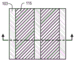
One embodiment includes a method for patterning a substrate. Fig. 1A to 18A and 1B to 18B illustrate an exemplary flow. Referring now to fig. 1A and 1B, a substrate 105 is provided having a mandrel layer 115 on a target layer 107. Note that one or more films may be located between mandrel layer 115 and target layer 107. A photoresist mandrel mask or etch mask 103 is formed over mandrel layer 115 (the layer where the mandrels are to be formed). Note that the photoresist mandrel mask may include any additional intermediate layers, such as planarizing layers, anti-reflective coatings, etc., so the etch mask 103 itself may not be in direct contact with the mandrel layer 115. In these and subsequent figures, the figures with "a" in the figures show a cross-sectional side view of an exemplary substrate section being processed, while the figures with "B" in the figures show a top view of the same substrate section, wherein the dashed cut lines show the positions of the respective cross-sectional side views. Note that for ease of identifying the material, the top view uses a material hatching (hatching) similar to that in the cross-sectional view, even though the top view does not show a cross-section but shows the top surface.
The mandrels 110 are formed on the target layer of the substrate using the etch mask 103, for example, with directional etching or anisotropic etching. Mandrel 110 comprises a first material and the target layer comprises a third material. Fig. 2A and 2B illustrate exemplary results.
Next, sidewall spacers 121 are formed on mandrel 110. Sidewall spacers may be formed by depositing a conformal film 120 over the substrate 105. Fig. 3A and 3B illustrate exemplary results of such conformal deposition. Note that such a film is deposited: having approximately the same thickness on both the horizontal and vertical surfaces. Portions of the conformal film on the top surface of mandrels 110 are removed, leaving the conformal film under the top surface of mandrels 110, such that sidewall spacers 121 are formed on the vertical sidewalls of mandrels 110 and such that the conformal film covers the target layer 107 between adjacent sidewall spacers. The conformal film includes a second material.
Various techniques exist to remove the top surface of the conformal film. In one alternative, the filler material 130 is deposited on the substrate. The fill material fills the trenches defined by the conformal film and typically has a capping layer (over-bump) of material. Fig. 4A and 4B illustrate exemplary results. A Chemical Mechanical Polishing (CMP) step may then be performed that removes the conformal film material and fill material 130 on the top surface of the mandrel 110. Fig. 5A and 5B illustrate exemplary results. Note that the substrate is planarized to the top surface of mandrel 110, leaving behind an insertion of filler material 130 in the trench defined by sidewall spacers 121.
Alternative techniques for removing the top surface of the conformal film are based on etching. A partial etch of the fill material 130 may be performed to expose the top surface of the conformal film 120. Exemplary results are shown in fig. 6A and 6B. For example, a plasma-based dry etch may be performed based on time or end point detection. Another option is wet etching, with a diffusion limited solubility transition on top of the fill material 130, so long as the fill material 130 is capable of solubility transition (developable). After exposing the top surface of the conformal film 120, a spacer opening etch may be performed to partially etch the conformal film until the top surface of the mandrel 110 is exposed. This leaves sidewall spacers 121 on mandrel 110. The conformal film material still covers the target layer 107 between the sidewall spacers 121 because the intervening portions of the fill material 130 prevent the underlying portions from being etched. Exemplary results are shown in fig. 7A and 7B. After the spacer opening etch is completed, the remaining fill material 130 may be removed, as shown in fig. 8A and 8B. A multi-line layer has then been created, but a portion of the spacer material covers the target layer 107 instead of being exposed or covered by a different material.
Referring now to fig. 9A and 9B, a first etch mask 141 is formed on the substrate. The fill material 131 may be deposited on the substrate prior to forming the etch mask as a planarization layer. The first etch mask 141 defines an opening exposing regions of both the first material (mandrel 110) and the second material (sidewall spacers 121). The first material and the second material have different etch resistance relative to each other. This means that for one or more specific etching chemistries, one of these materials can be selectively etched while the other material is not etched, meaning that either no etching occurs or an insignificant amount of one material is etched away compared to the other material, e.g., by having an etch rate four or more times slower. Although only two materials are seen from the top view through the etch mask, due to the difference in height of the conformal film between the sidewall spacers, the height deviation effectively provides three lines of material such that the etch mask 141 can be further narrowed for etch location selection by three alternating lines of material, but only two etch chemistry-based materials are required. Both of these materials may be selected to be etchable using non-corrosive etching chemistries.
With the etch mask 141 in place on the substrate, uncovered portions of the fill material 131 may be removed, such as by directional etching. Removing the portion of fill material 131 exposes mandrels 110 and sidewall spacers 121. Fig. 10A and 10B show the substrate after this step.
A first etching process is performed that selectively etches uncovered portions of the second material until the conformal film covering the target layer 107 between adjacent sidewall spacers 121 is removed, while the sidewall spacers 121 remain on the substrate. Exemplary results are shown in fig. 11A and 11B. Note that portions of the target layer 107 are now visible from above, meaning that these portions are now exposed. Note also that this first etching process shortens the height of the sidewall spacers 121. The fill material 131 and the etch mask 141 may then be removed as shown in fig. 12A and 12B.
Referring now to fig. 13A and 13B, a second etch mask 142 is formed on the substrate. A fill material 132 may be deposited on the substrate prior to forming the etch mask. The second etch mask 142 defines an opening exposing regions of both the first material (mandrel 110) and the second material (sidewall spacers 121). The first material and the second material have different etch resistance relative to each other.
With the etch mask 142 in place on the substrate, uncovered portions of the fill material 132 may be removed, such as by directional etching. Removing the portion of fill material 132 exposes mandrels 110 and sidewall spacers 121. Fig. 14A and 14B show the substrate after this step.
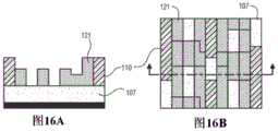
A second etching process is performed that selectively etches the uncovered portions of the first material until the uncovered mandrels 110 are removed. Exemplary results are shown in fig. 15A and 15B. Note that portions of the target layer 107 are now visible from above, meaning that these portions are now exposed. The fill material 132 and etch mask 142 may then be removed, as shown in fig. 16A and 16B.
The conformal film covering the target layer between adjacent sidewall spacers, and the remainder of the mandrels together form a combined relief pattern, which can be used as an etch mask to transfer into the target layer 107 or other memory layer. Fig. 17A and 17B show the result of etching the uncovered portion of the target layer 107. Fig. 18A and 18B then illustrate the patterned target layer 107 after pattern transfer is completed. Thus, features that are sub-resolution and that are formed without a corrosive etch can be created.
Fig. 19A to 32A and fig. 19B to 32B illustrate another exemplary embodiment. Referring now to fig. 19A and 19B, a substrate 105 is provided having a mandrel layer 115 on a target layer 107. Note that one or more films may be located between mandrel layer 115 and target layer 107. A photoresist mandrel mask or etch mask 103 is formed over the mandrel layer.
A mandrel 110 is then formed over the target layer 107 of the substrate. The mandrel comprises a first material and the target layer comprises a third material. A film 116 of the first material covers the target layer between the mandrels such that the top surface of mandrel 110 is higher in height than the top surface of the film of the first material. The height difference is at least twice the thickness of the film 116 of the first material. This is shown in fig. 20A and 20B. Such mandrels may be formed by partially etching through a layer of the first material, but not completely etching through the layer of the first material. This partial etch leaves substantially a relatively small thickness of the first material on the target layer as part of the process of forming mandrel 110.
A conformal film 120 can then be deposited over the substrate, as shown in fig. 21A and 21B. A spacer opening etch may be performed to form sidewall spacers 121, as shown in fig. 22A and 22B. The sidewall spacers 121 comprise a second material. The sidewall spacers 121 define open spaces between each other that expose the film 116 of the first material.
The substrate may be planarized with the filling material 131 and then a first etching mask 141 may be formed thereon, as shown in fig. 23A and 23B. The uncovered fill material 131 can be etched to expose the multi-line layer as shown in fig. 24A and 24B. Next, optionally, the uncovered film 116 of the first material may be etched until the target layer 107 is exposed. Note that the uncovered mandrels will also be etched in the same amount/rate as the film of the first material, so the height of these uncovered mandrels will be reduced, but still have sufficient height to cover the substrate. Fig. 25A and 25B show exemplary results. The remaining fill material 132 and etch mask material may be removed as shown in fig. 26A and 26B.
The substrate may be planarized with the fill material 132 and then a second etch mask 142 may be formed thereon, as shown in fig. 27A and 27B. The uncovered fill material 132 can be etched to expose the multi-line layer as shown in fig. 28A and 28B. Next, optionally, uncovered mandrels 110 can be etched until target layer 107 is exposed. Fig. 29A and 29B show exemplary results. The remaining fill material 132 and etch mask material may be removed as shown in fig. 30A and 30B.
Together, the film of the first material, the sidewall spacers, and the remainder of the mandrel form a combined relief pattern, which can be used as an etch mask to transfer into the target layer 107 or other memory layer. Fig. 31A and 31B show the result of etching the uncovered portion of the target layer 107. Fig. 32A and 32B then illustrate the patterned target layer 107 after pattern transfer is completed.
Fig. 33A to 46A and 33B to 46B illustrate another exemplary embodiment. Referring now to fig. 33A and 33B, a substrate 105 is provided having a mandrel layer 115 positioned over a target layer 107. A photoresist mandrel mask or etch mask 103 is formed over the mandrel layer. Mandrel layer 115 may be formed as a three-layer stack on target layer 107. The three-layer stack includes a bottom layer 111, a middle layer 112, and an upper layer 113, each of which is deposited as a horizontal and uniform layer. The upper layer 113 includes a first material, the intermediate layer 112 includes a fifth material, the bottom layer 111 includes a sixth material, and the target layer 107 includes a third material.
A mandrel 110 is then formed on the target layer 107 of the substrate by using the etch mask 103 and performing a first etch process that etches a mandrel pattern into the upper layer 113 until the intermediate layer 112 is exposed, and the mandrel 110 comprises a first material. The intermediate layer has a different etch resistance than the upper layer such that the intermediate layer provides an etch stop layer for the etching process to form the mandrel. Fig. 34A and 34B show exemplary results.
A conformal film 120 can then be deposited over the substrate, as shown in fig. 35A and 35B. A spacer opening etch may be performed to form sidewall spacers 121 as shown in fig. 36A and 36B. The sidewall spacers 121 comprise a second material. The sidewall spacers define open spaces between each other that expose the bottom layer 111. Note that different etch chemistries may be used to etch the conformal film 120 and the intermediate layer 112. Alternatively, the conformal film 120 and the intermediate layer 112 may be the same material or have the same etch resistance to enable etching of both materials with the same etch chemistry.
The substrate may be planarized with the filling material 131 and then a first etching mask 141 may be formed thereon, as shown in fig. 37A and 37B. The uncovered fill material 131 can be etched to expose the multi-line layer as shown in fig. 38A and 38B. Next, optionally, uncovered portions of the underlayer 111 may be etched until the underlayer 111 covering the target layer between adjacent sidewall spacers is removed, while the sidewall spacers remain on the substrate. The results are shown in fig. 39A and 39B. Note that if both materials have the same etch resistance, the uncovered mandrels can also be etched away in the same amount as the underlying layers. The remaining fill material 132 and etch mask material may be removed as shown in fig. 40A and 40B.
The substrate may be planarized with the fill material 132 and then a second etch mask 142 may be formed thereon, as shown in fig. 41A and 41B. The uncovered fill material 132 can be etched to expose the multi-line layer as shown in fig. 42A and 42B. Next, optionally, the uncovered mandrels 110 can be etched until the intermediate layer 112 is exposed, then the uncovered portions of the intermediate layer, then the uncovered portions of the bottom layer 111 are etched until the target layer 107 is exposed. Fig. 43A and 43B show exemplary results. The remaining fill material 132 and etch mask material may be removed as shown in fig. 44A and 44B.
Together, the film of the first material, the sidewall spacers, and the remainder of the mandrel form a combined relief pattern, which can be used as an etch mask to transfer into the target layer 107 or other memory layer. Fig. 45A and 45B show the result of etching the uncovered portion of the target layer 107. Fig. 46A and 46B then illustrate the patterned target layer 107 after pattern transfer is completed.
In the previous description, specific details have been set forth, such as specific geometries of processing systems and descriptions of various components and processes used therein. However, it should be understood that the techniques herein may be practiced in other embodiments that depart from these specific details, and that these details are for purposes of illustration and not limitation. Embodiments disclosed herein have been described with reference to the accompanying drawings. Similarly, for purposes of explanation, specific numbers, materials and configurations are set forth in order to provide a thorough understanding. However, embodiments may be practiced without such specific details. Parts having substantially the same functional configuration are denoted by the same reference numerals, and thus any redundant description may be omitted.
Various techniques have been described as multiple separate operations to aid in the understanding of the various embodiments. The order of description should not be construed as to imply that these operations are necessarily order dependent. Indeed, these operations need not be performed in the order of presentation. The described operations may be performed in a different order than the described embodiments. In further embodiments, various additional operations may be performed and/or described operations may be omitted.
As used herein, "substrate" or "target substrate" generally refers to an object being processed in accordance with the present invention. The substrate may comprise any material portion or structure of a device, in particular a semiconductor or other electronic device, and may be, for example, a base substrate structure (e.g., a semiconductor wafer, a reticle) or a layer (e.g., a thin film) on or covering the base substrate structure. Thus, the substrate is not limited to any particular underlying structure, layer or coating, patterned or unpatterned, but is intended to include any such layer or underlying structure, and any combination of layers and/or underlying structures. The description may refer to a particular type of substrate, but this is for illustrative purposes only.
Those skilled in the art will also appreciate that many modifications may be made to the operation of the techniques described above, while still achieving the same objectives of the invention. Such variations are intended to be covered by the scope of this disclosure. As such, the foregoing description of embodiments of the invention is not intended to be limiting. Rather, any limitations to the embodiments of the invention are presented in the appended claims.
Claims (15)
1. A method of patterning a substrate, the method comprising:
forming a mandrel on a target layer of a substrate, the mandrel comprising a first material, the target layer comprising a third material;
forming sidewall spacers on sidewalls of the mandrels, comprising depositing a conformal film on the substrate and removing portions of the conformal film on a top surface of the mandrels while leaving the conformal film under the top surface of the mandrels such that the sidewall spacers are formed on vertical sidewalls of the mandrels and such that the conformal film covers the target layer between adjacent sidewall spacers, the conformal film comprising a second material;
forming a first etch mask on the substrate, the first etch mask defining an opening exposing regions of both the first material and the second material, the first material and the second material having different etch resistance; and
performing a first etch process that selectively etches exposed portions of the second material until the conformal film covering the target layer between adjacent sidewall spacers is removed, while the sidewall spacers remain on the substrate,
forming a second etch mask on the substrate, the second etch mask defining an opening exposing regions of both the first material and the second material; and
a second etching process is performed that selectively etches the exposed portions of the first material until the exposed mandrels are removed.
2. The method of claim 1, wherein forming the sidewall spacers comprises: depositing a second filler material on the substrate, the second filler material filling a trench defined by the conformal film; and
a chemical mechanical polishing step is performed that removes the conformal film material and the second filler material over the top surface of the mandrel.
3. The method of claim 2, further comprising removing the second filler material from the trench defined by the conformal film.
4. The method of claim 1, wherein forming the sidewall spacers comprises: depositing a second filler material on the substrate, the second filler material filling a trench defined by the conformal film;
performing a third etching process that etches the second filler material until a top surface of the conformal film is exposed;
a fourth etching process is performed that etches the conformal film until a top surface of the mandrel is exposed.
5. The method of claim 4, further comprising removing the second filler material from the substrate.
6. The method of claim 1, further comprising:
removing the first etch mask after performing the first etch process and before forming the second etch mask; and
the second etch mask is removed after performing the second etch process, covering the conformal film of the target layer between adjacent sidewall spacers, the sidewall spacers, and the remaining portions of the mandrels, together forming a combined relief pattern.
7. The method of claim 6, further comprising performing a fifth etching process using the combined relief pattern as an etching mask and transferring a corresponding pattern into the target layer.
8. The method of claim 1, wherein forming the first etch mask comprises: depositing a first filler material on the substrate to planarize the substrate, wherein the first etch mask is formed on the first filler material, the first filler material comprising a fourth material, the first and second and third and fourth materials having different etch resistance relative to each other.
9. The method of claim 2, wherein forming the second etch mask comprises: depositing a second filler material on the substrate to planarize the substrate, wherein the second etch mask is formed on the second filler material, the second filler material comprising a fourth material, the first and second and third and fourth materials having different etch resistance relative to each other.
10. A method of patterning a substrate, the method comprising:
forming mandrels on a target layer of a substrate, the mandrels comprising a first material and the target layer comprising a third material, in which a film of the first material covers the target layer between the mandrels such that a top surface of the mandrels is higher in height than a top surface of the film of the first material;
forming sidewall spacers on sidewalls of the mandrel, the sidewall spacers comprising a second material, the sidewall spacers defining open spaces between each other, the open spaces exposing a film of the first material;
depositing a filler material on the substrate, the filler material at least partially filling the open spaces defined between the sidewall spacers, the filler material comprising a fourth material, wherein the first material, the third material, and the fourth material are all chemically different from one another; and
performing a first etching process that etches the exposed portion of the fill material and etches the exposed portion of the top layer of the mandrel,
forming a second etch mask on the substrate, the second etch mask defining an opening exposing regions of both the first material and the second material; and
a second etching process is performed that selectively etches the exposed portion of the first material until the target layer is exposed.
11. A method of patterning a substrate, the method comprising:
forming a three-layer stack on a target layer, the three-layer stack comprising a bottom layer, an intermediate layer, and an upper layer, each layer deposited as a horizontal and uniform layer, the upper layer comprising a first material, the intermediate layer comprising a fifth material, the bottom layer comprising a sixth material, the target layer comprising a third material;
forming a mandrel comprising the first material by using a first etch mask and performing a first etch process that etches a mandrel pattern into the upper layer until the intermediate layer is exposed, the intermediate layer having a different etch resistance than the upper layer such that the intermediate layer provides an etch stop layer for the first etch process;
forming sidewall spacers on sidewalls of the mandrel, the sidewall spacers comprising a second material, the sidewall spacers defining open spaces between each other, the open spaces exposing the bottom layer;
forming a second etch mask on the substrate, the second etch mask defining an opening exposing regions of both the first material and the second material, the first material and the second material having different etch resistance; and
a second etching process is performed that selectively etches the exposed portions of the sixth material until the bottom layer covering the target layer between adjacent sidewall spacers is removed, while the sidewall spacers remain on the substrate.
12. The method of claim 11, further comprising:
forming a third etch mask on the substrate, the third etch mask defining openings exposing regions of both the first material and the second material, the first material and the second material having different etch resistance; and
a third etching process is performed that selectively etches the exposed portion of the mandrel until the intermediate layer is exposed, then etches the exposed portion of the intermediate layer, and then etches the exposed portion of the bottom layer until the target layer is exposed.
13. The method of claim 11, wherein the first material and the sixth material have the same etch resistance.
14. The method of claim 11, wherein the fifth material and the second material have the same etch resistance.
15. The method of claim 11, wherein the etch stop layer and the sidewall spacers comprise the same material.
Applications Claiming Priority (3)
| Application Number | Priority Date | Filing Date | Title |
|---|---|---|---|
| US201662340279P | 2016-05-23 | 2016-05-23 | |
| US62/340,279 | 2016-05-23 | ||
| PCT/US2017/033051 WO2017205136A1 (en) | 2016-05-23 | 2017-05-17 | Method for patterning a substrate using a layer with multiple materials |
Publications (2)
| Publication Number | Publication Date |
|---|---|
| CN109155238A CN109155238A (en) | 2019-01-04 |
| CN109155238B true CN109155238B (en) | 2023-04-21 |
Family
ID=60330321
Family Applications (1)
| Application Number | Title | Priority Date | Filing Date |
|---|---|---|---|
| CN201780032238.4A Active CN109155238B (en) | 2016-05-23 | 2017-05-17 | Method for patterning a substrate using a layer having multiple materials |
Country Status (7)
| Country | Link |
|---|---|
| US (1) | US10366890B2 (en) |
| JP (1) | JP7008907B2 (en) |
| KR (1) | KR102296805B1 (en) |
| CN (1) | CN109155238B (en) |
| SG (1) | SG11201810373YA (en) |
| TW (1) | TWI657484B (en) |
| WO (1) | WO2017205136A1 (en) |
Families Citing this family (12)
| Publication number | Priority date | Publication date | Assignee | Title |
|---|---|---|---|---|
| KR102303129B1 (en) * | 2016-10-20 | 2021-09-15 | 도쿄엘렉트론가부시키가이샤 | Methods for Reducing Overlay Errors in Via-to-Grid Patterning |
| US11901190B2 (en) * | 2017-11-30 | 2024-02-13 | Taiwan Semiconductor Manufacturing Company, Ltd. | Method of patterning |
| US11127594B2 (en) * | 2017-12-19 | 2021-09-21 | Tokyo Electron Limited | Manufacturing methods for mandrel pull from spacers for multi-color patterning |
| US10366917B2 (en) | 2018-01-04 | 2019-07-30 | Globalfoundries Inc. | Methods of patterning variable width metallization lines |
| KR102617139B1 (en) * | 2018-04-09 | 2023-12-26 | 삼성전자주식회사 | Semiconductor device and manufacturing method thereof |
| US10573520B2 (en) | 2018-06-12 | 2020-02-25 | International Business Machines Corporation | Multiple patterning scheme integration with planarized cut patterning |
| US11061315B2 (en) * | 2018-11-15 | 2021-07-13 | Globalfoundries U.S. Inc. | Hybrid optical and EUV lithography |
| US10529570B1 (en) * | 2018-11-20 | 2020-01-07 | Nanya Technology Corporation | Method for preparing a semiconductor structure |
| US11069564B2 (en) | 2019-04-09 | 2021-07-20 | International Business Machines Corporation | Double metal patterning |
| CN110289221B (en) * | 2019-06-25 | 2021-06-29 | 武汉新芯集成电路制造有限公司 | Semiconductor device and manufacturing method thereof |
| EP3840034B1 (en) | 2019-12-19 | 2022-06-15 | Imec VZW | Method for producing nanoscaled electrically conductive lines for semiconductor devices |
| CN111162447B (en) * | 2019-12-31 | 2021-06-15 | 苏州辰睿光电有限公司 | Electrode window and manufacturing method of semiconductor device with electrode window |
Citations (4)
| Publication number | Priority date | Publication date | Assignee | Title |
|---|---|---|---|---|
| CN1941322A (en) * | 2005-09-29 | 2007-04-04 | 海力士半导体有限公司 | Method for forming metal line in flash memory device |
| CN101030532A (en) * | 2006-02-27 | 2007-09-05 | 海力士半导体有限公司 | Method for fabricating semiconductor device |
| JP2011165933A (en) * | 2010-02-10 | 2011-08-25 | Toshiba Corp | Method of manufacturing semiconductor device |
| JP2014093450A (en) * | 2012-11-05 | 2014-05-19 | Dainippon Printing Co Ltd | Pattern structure forming method |
Family Cites Families (21)
| Publication number | Priority date | Publication date | Assignee | Title |
|---|---|---|---|---|
| KR100771891B1 (en) | 2006-11-10 | 2007-11-01 | 삼성전자주식회사 | Method of forming fine patterns of semiconductor device using double patterning process |
| KR100825796B1 (en) * | 2006-12-14 | 2008-04-28 | 삼성전자주식회사 | Method of manufacturing semiconductor device having buried gate |
| US8600391B2 (en) | 2008-11-24 | 2013-12-03 | Ringcentral, Inc. | Call management for location-aware mobile devices |
| US8670545B2 (en) | 2007-09-28 | 2014-03-11 | Ringcentral, Inc. | Inbound call identification and management |
| US8838082B2 (en) | 2008-11-26 | 2014-09-16 | Ringcentral, Inc. | Centralized status server for call management of location-aware mobile devices |
| US20090130854A1 (en) * | 2007-11-21 | 2009-05-21 | Macronix International Co., Ltd. | Patterning structure and method for semiconductor devices |
| JP5484325B2 (en) | 2008-06-13 | 2014-05-07 | 東京エレクトロン株式会社 | Manufacturing method of semiconductor device |
| US7915105B2 (en) * | 2008-11-06 | 2011-03-29 | Taiwan Semiconductor Manufacturing Company, Ltd. | Method for patterning a metal gate |
| US8492282B2 (en) | 2008-11-24 | 2013-07-23 | Micron Technology, Inc. | Methods of forming a masking pattern for integrated circuits |
| KR100995142B1 (en) * | 2008-12-22 | 2010-11-18 | 주식회사 하이닉스반도체 | Method of fabricating contact hole in semiconductor device |
| JP2014072226A (en) | 2012-09-27 | 2014-04-21 | Tokyo Electron Ltd | Pattern formation method |
| US9362133B2 (en) * | 2012-12-14 | 2016-06-07 | Lam Research Corporation | Method for forming a mask by etching conformal film on patterned ashable hardmask |
| US8828876B2 (en) | 2013-01-09 | 2014-09-09 | International Business Machines Corporation | Dual mandrel sidewall image transfer processes |
| US9006804B2 (en) * | 2013-06-06 | 2015-04-14 | United Microelectronics Corp. | Semiconductor device and fabrication method thereof |
| TWI531032B (en) * | 2013-11-21 | 2016-04-21 | 力晶科技股份有限公司 | Memory circuit structure and semiconductor process for manufacturing the same |
| US9209076B2 (en) | 2013-11-22 | 2015-12-08 | Taiwan Semiconductor Manufacturing Company, Ltd. | Method of double patterning lithography process using plurality of mandrels for integrated circuit applications |
| WO2015126829A1 (en) * | 2014-02-23 | 2015-08-27 | Tokyo Electron Limited | Method for patterning a substrate for planarization |
| US9508713B2 (en) | 2014-03-05 | 2016-11-29 | International Business Machines Corporation | Densely spaced fins for semiconductor fin field effect transistors |
| US9123656B1 (en) | 2014-05-13 | 2015-09-01 | Taiwan Semiconductor Manufacturing Co., Ltd. | Organosilicate polymer mandrel for self-aligned double patterning process |
| FR3025937B1 (en) * | 2014-09-16 | 2017-11-24 | Commissariat Energie Atomique | GRAPHO-EPITAXY METHOD FOR REALIZING PATTERNS ON THE SURFACE OF A SUBSTRATE |
| US9780193B2 (en) * | 2015-10-27 | 2017-10-03 | United Microelectronics Corporation | Device with reinforced metal gate spacer and method of fabricating |
-
2017
- 2017-05-16 US US15/596,618 patent/US10366890B2/en active Active
- 2017-05-17 SG SG11201810373YA patent/SG11201810373YA/en unknown
- 2017-05-17 JP JP2018561727A patent/JP7008907B2/en active Active
- 2017-05-17 WO PCT/US2017/033051 patent/WO2017205136A1/en active Application Filing
- 2017-05-17 KR KR1020187037358A patent/KR102296805B1/en active IP Right Grant
- 2017-05-17 CN CN201780032238.4A patent/CN109155238B/en active Active
- 2017-05-19 TW TW106116566A patent/TWI657484B/en active
Patent Citations (4)
| Publication number | Priority date | Publication date | Assignee | Title |
|---|---|---|---|---|
| CN1941322A (en) * | 2005-09-29 | 2007-04-04 | 海力士半导体有限公司 | Method for forming metal line in flash memory device |
| CN101030532A (en) * | 2006-02-27 | 2007-09-05 | 海力士半导体有限公司 | Method for fabricating semiconductor device |
| JP2011165933A (en) * | 2010-02-10 | 2011-08-25 | Toshiba Corp | Method of manufacturing semiconductor device |
| JP2014093450A (en) * | 2012-11-05 | 2014-05-19 | Dainippon Printing Co Ltd | Pattern structure forming method |
Also Published As
| Publication number | Publication date |
|---|---|
| WO2017205136A1 (en) | 2017-11-30 |
| TW201812847A (en) | 2018-04-01 |
| KR102296805B1 (en) | 2021-08-31 |
| JP2019517154A (en) | 2019-06-20 |
| KR20190000918A (en) | 2019-01-03 |
| CN109155238A (en) | 2019-01-04 |
| US20170338116A1 (en) | 2017-11-23 |
| SG11201810373YA (en) | 2018-12-28 |
| JP7008907B2 (en) | 2022-01-25 |
| TWI657484B (en) | 2019-04-21 |
| US10366890B2 (en) | 2019-07-30 |
Similar Documents
| Publication | Publication Date | Title |
|---|---|---|
| CN109155238B (en) | Method for patterning a substrate using a layer having multiple materials | |
| TWI622861B (en) | Methods of forming etch masks for sub-resolution substrate patterning | |
| CN108369899B (en) | Method of forming an etch mask for sub-resolution substrate patterning | |
| US11107682B2 (en) | Method for patterning a substrate using a layer with multiple materials | |
| CN108701588B (en) | Method and system for forming memory fin patterns | |
| JP2018531506A6 (en) | Method of forming an etching mask for sub-resolution substrate patterning | |
| CN109075124B (en) | Method for patterning a substrate using a layer having multiple materials | |
| CN109983564B (en) | Method for sub-resolution substrate patterning | |
| WO2021025806A1 (en) | Method for increasing pattern density on a wafer |
Legal Events
| Date | Code | Title | Description |
|---|---|---|---|
| PB01 | Publication | ||
| PB01 | Publication | ||
| SE01 | Entry into force of request for substantive examination | ||
| SE01 | Entry into force of request for substantive examination | ||
| GR01 | Patent grant | ||
| GR01 | Patent grant |