JP6724851B2 - Base material, mold package using the same, base material manufacturing method, and mold package manufacturing method - Google Patents
Base material, mold package using the same, base material manufacturing method, and mold package manufacturing method Download PDFInfo
- Publication number
- JP6724851B2 JP6724851B2 JP2017080679A JP2017080679A JP6724851B2 JP 6724851 B2 JP6724851 B2 JP 6724851B2 JP 2017080679 A JP2017080679 A JP 2017080679A JP 2017080679 A JP2017080679 A JP 2017080679A JP 6724851 B2 JP6724851 B2 JP 6724851B2
- Authority
- JP
- Japan
- Prior art keywords
- region
- concavo
- convex
- metal particles
- forming
- Prior art date
- Legal status (The legal status is an assumption and is not a legal conclusion. Google has not performed a legal analysis and makes no representation as to the accuracy of the status listed.)
- Active
Links
Images


Classifications
-
- H—ELECTRICITY
- H01—ELECTRIC ELEMENTS
- H01L—SEMICONDUCTOR DEVICES NOT COVERED BY CLASS H10
- H01L24/00—Arrangements for connecting or disconnecting semiconductor or solid-state bodies; Methods or apparatus related thereto
- H01L24/80—Methods for connecting semiconductor or other solid state bodies using means for bonding being attached to, or being formed on, the surface to be connected
- H01L24/85—Methods for connecting semiconductor or other solid state bodies using means for bonding being attached to, or being formed on, the surface to be connected using a wire connector
-
- H—ELECTRICITY
- H01—ELECTRIC ELEMENTS
- H01L—SEMICONDUCTOR DEVICES NOT COVERED BY CLASS H10
- H01L23/00—Details of semiconductor or other solid state devices
- H01L23/48—Arrangements for conducting electric current to or from the solid state body in operation, e.g. leads, terminal arrangements ; Selection of materials therefor
- H01L23/488—Arrangements for conducting electric current to or from the solid state body in operation, e.g. leads, terminal arrangements ; Selection of materials therefor consisting of soldered or bonded constructions
- H01L23/495—Lead-frames or other flat leads
- H01L23/49503—Lead-frames or other flat leads characterised by the die pad
- H01L23/49513—Lead-frames or other flat leads characterised by the die pad having bonding material between chip and die pad
-
- H—ELECTRICITY
- H01—ELECTRIC ELEMENTS
- H01L—SEMICONDUCTOR DEVICES NOT COVERED BY CLASS H10
- H01L21/00—Processes or apparatus adapted for the manufacture or treatment of semiconductor or solid state devices or of parts thereof
- H01L21/02—Manufacture or treatment of semiconductor devices or of parts thereof
- H01L21/04—Manufacture or treatment of semiconductor devices or of parts thereof the devices having at least one potential-jump barrier or surface barrier, e.g. PN junction, depletion layer or carrier concentration layer
- H01L21/48—Manufacture or treatment of parts, e.g. containers, prior to assembly of the devices, using processes not provided for in a single one of the subgroups H01L21/06 - H01L21/326
- H01L21/4814—Conductive parts
- H01L21/4821—Flat leads, e.g. lead frames with or without insulating supports
-
- H—ELECTRICITY
- H01—ELECTRIC ELEMENTS
- H01L—SEMICONDUCTOR DEVICES NOT COVERED BY CLASS H10
- H01L21/00—Processes or apparatus adapted for the manufacture or treatment of semiconductor or solid state devices or of parts thereof
- H01L21/02—Manufacture or treatment of semiconductor devices or of parts thereof
- H01L21/04—Manufacture or treatment of semiconductor devices or of parts thereof the devices having at least one potential-jump barrier or surface barrier, e.g. PN junction, depletion layer or carrier concentration layer
- H01L21/50—Assembly of semiconductor devices using processes or apparatus not provided for in a single one of the subgroups H01L21/06 - H01L21/326, e.g. sealing of a cap to a base of a container
- H01L21/56—Encapsulations, e.g. encapsulation layers, coatings
- H01L21/565—Moulds
-
- H—ELECTRICITY
- H01—ELECTRIC ELEMENTS
- H01L—SEMICONDUCTOR DEVICES NOT COVERED BY CLASS H10
- H01L23/00—Details of semiconductor or other solid state devices
- H01L23/28—Encapsulations, e.g. encapsulating layers, coatings, e.g. for protection
- H01L23/29—Encapsulations, e.g. encapsulating layers, coatings, e.g. for protection characterised by the material, e.g. carbon
- H01L23/293—Organic, e.g. plastic
-
- H—ELECTRICITY
- H01—ELECTRIC ELEMENTS
- H01L—SEMICONDUCTOR DEVICES NOT COVERED BY CLASS H10
- H01L23/00—Details of semiconductor or other solid state devices
- H01L23/28—Encapsulations, e.g. encapsulating layers, coatings, e.g. for protection
- H01L23/31—Encapsulations, e.g. encapsulating layers, coatings, e.g. for protection characterised by the arrangement or shape
- H01L23/3107—Encapsulations, e.g. encapsulating layers, coatings, e.g. for protection characterised by the arrangement or shape the device being completely enclosed
- H01L23/3121—Encapsulations, e.g. encapsulating layers, coatings, e.g. for protection characterised by the arrangement or shape the device being completely enclosed a substrate forming part of the encapsulation
-
- H—ELECTRICITY
- H01—ELECTRIC ELEMENTS
- H01L—SEMICONDUCTOR DEVICES NOT COVERED BY CLASS H10
- H01L23/00—Details of semiconductor or other solid state devices
- H01L23/28—Encapsulations, e.g. encapsulating layers, coatings, e.g. for protection
- H01L23/31—Encapsulations, e.g. encapsulating layers, coatings, e.g. for protection characterised by the arrangement or shape
- H01L23/3107—Encapsulations, e.g. encapsulating layers, coatings, e.g. for protection characterised by the arrangement or shape the device being completely enclosed
- H01L23/3142—Sealing arrangements between parts, e.g. adhesion promotors
-
- H—ELECTRICITY
- H01—ELECTRIC ELEMENTS
- H01L—SEMICONDUCTOR DEVICES NOT COVERED BY CLASS H10
- H01L23/00—Details of semiconductor or other solid state devices
- H01L23/48—Arrangements for conducting electric current to or from the solid state body in operation, e.g. leads, terminal arrangements ; Selection of materials therefor
- H01L23/488—Arrangements for conducting electric current to or from the solid state body in operation, e.g. leads, terminal arrangements ; Selection of materials therefor consisting of soldered or bonded constructions
- H01L23/495—Lead-frames or other flat leads
- H01L23/49541—Geometry of the lead-frame
- H01L23/49548—Cross section geometry
-
- H—ELECTRICITY
- H01—ELECTRIC ELEMENTS
- H01L—SEMICONDUCTOR DEVICES NOT COVERED BY CLASS H10
- H01L23/00—Details of semiconductor or other solid state devices
- H01L23/48—Arrangements for conducting electric current to or from the solid state body in operation, e.g. leads, terminal arrangements ; Selection of materials therefor
- H01L23/488—Arrangements for conducting electric current to or from the solid state body in operation, e.g. leads, terminal arrangements ; Selection of materials therefor consisting of soldered or bonded constructions
- H01L23/495—Lead-frames or other flat leads
- H01L23/49541—Geometry of the lead-frame
- H01L23/49562—Geometry of the lead-frame for devices being provided for in H01L29/00
-
- H—ELECTRICITY
- H01—ELECTRIC ELEMENTS
- H01L—SEMICONDUCTOR DEVICES NOT COVERED BY CLASS H10
- H01L23/00—Details of semiconductor or other solid state devices
- H01L23/48—Arrangements for conducting electric current to or from the solid state body in operation, e.g. leads, terminal arrangements ; Selection of materials therefor
- H01L23/488—Arrangements for conducting electric current to or from the solid state body in operation, e.g. leads, terminal arrangements ; Selection of materials therefor consisting of soldered or bonded constructions
- H01L23/495—Lead-frames or other flat leads
- H01L23/49579—Lead-frames or other flat leads characterised by the materials of the lead frames or layers thereon
- H01L23/49582—Metallic layers on lead frames
-
- H—ELECTRICITY
- H01—ELECTRIC ELEMENTS
- H01L—SEMICONDUCTOR DEVICES NOT COVERED BY CLASS H10
- H01L2224/00—Indexing scheme for arrangements for connecting or disconnecting semiconductor or solid-state bodies and methods related thereto as covered by H01L24/00
- H01L2224/01—Means for bonding being attached to, or being formed on, the surface to be connected, e.g. chip-to-package, die-attach, "first-level" interconnects; Manufacturing methods related thereto
- H01L2224/26—Layer connectors, e.g. plate connectors, solder or adhesive layers; Manufacturing methods related thereto
- H01L2224/28—Structure, shape, material or disposition of the layer connectors prior to the connecting process
- H01L2224/29—Structure, shape, material or disposition of the layer connectors prior to the connecting process of an individual layer connector
- H01L2224/29001—Core members of the layer connector
- H01L2224/29099—Material
- H01L2224/291—Material with a principal constituent of the material being a metal or a metalloid, e.g. boron [B], silicon [Si], germanium [Ge], arsenic [As], antimony [Sb], tellurium [Te] and polonium [Po], and alloys thereof
- H01L2224/29138—Material with a principal constituent of the material being a metal or a metalloid, e.g. boron [B], silicon [Si], germanium [Ge], arsenic [As], antimony [Sb], tellurium [Te] and polonium [Po], and alloys thereof the principal constituent melting at a temperature of greater than or equal to 950°C and less than 1550°C
- H01L2224/29139—Silver [Ag] as principal constituent
-
- H—ELECTRICITY
- H01—ELECTRIC ELEMENTS
- H01L—SEMICONDUCTOR DEVICES NOT COVERED BY CLASS H10
- H01L2224/00—Indexing scheme for arrangements for connecting or disconnecting semiconductor or solid-state bodies and methods related thereto as covered by H01L24/00
- H01L2224/01—Means for bonding being attached to, or being formed on, the surface to be connected, e.g. chip-to-package, die-attach, "first-level" interconnects; Manufacturing methods related thereto
- H01L2224/26—Layer connectors, e.g. plate connectors, solder or adhesive layers; Manufacturing methods related thereto
- H01L2224/31—Structure, shape, material or disposition of the layer connectors after the connecting process
- H01L2224/32—Structure, shape, material or disposition of the layer connectors after the connecting process of an individual layer connector
- H01L2224/321—Disposition
- H01L2224/32151—Disposition the layer connector connecting between a semiconductor or solid-state body and an item not being a semiconductor or solid-state body, e.g. chip-to-substrate, chip-to-passive
- H01L2224/32221—Disposition the layer connector connecting between a semiconductor or solid-state body and an item not being a semiconductor or solid-state body, e.g. chip-to-substrate, chip-to-passive the body and the item being stacked
- H01L2224/32245—Disposition the layer connector connecting between a semiconductor or solid-state body and an item not being a semiconductor or solid-state body, e.g. chip-to-substrate, chip-to-passive the body and the item being stacked the item being metallic
-
- H—ELECTRICITY
- H01—ELECTRIC ELEMENTS
- H01L—SEMICONDUCTOR DEVICES NOT COVERED BY CLASS H10
- H01L2224/00—Indexing scheme for arrangements for connecting or disconnecting semiconductor or solid-state bodies and methods related thereto as covered by H01L24/00
- H01L2224/01—Means for bonding being attached to, or being formed on, the surface to be connected, e.g. chip-to-package, die-attach, "first-level" interconnects; Manufacturing methods related thereto
- H01L2224/42—Wire connectors; Manufacturing methods related thereto
- H01L2224/44—Structure, shape, material or disposition of the wire connectors prior to the connecting process
- H01L2224/45—Structure, shape, material or disposition of the wire connectors prior to the connecting process of an individual wire connector
- H01L2224/45001—Core members of the connector
- H01L2224/45099—Material
- H01L2224/451—Material with a principal constituent of the material being a metal or a metalloid, e.g. boron (B), silicon (Si), germanium (Ge), arsenic (As), antimony (Sb), tellurium (Te) and polonium (Po), and alloys thereof
- H01L2224/45117—Material with a principal constituent of the material being a metal or a metalloid, e.g. boron (B), silicon (Si), germanium (Ge), arsenic (As), antimony (Sb), tellurium (Te) and polonium (Po), and alloys thereof the principal constituent melting at a temperature of greater than or equal to 400°C and less than 950°C
- H01L2224/45124—Aluminium (Al) as principal constituent
-
- H—ELECTRICITY
- H01—ELECTRIC ELEMENTS
- H01L—SEMICONDUCTOR DEVICES NOT COVERED BY CLASS H10
- H01L2224/00—Indexing scheme for arrangements for connecting or disconnecting semiconductor or solid-state bodies and methods related thereto as covered by H01L24/00
- H01L2224/01—Means for bonding being attached to, or being formed on, the surface to be connected, e.g. chip-to-package, die-attach, "first-level" interconnects; Manufacturing methods related thereto
- H01L2224/42—Wire connectors; Manufacturing methods related thereto
- H01L2224/44—Structure, shape, material or disposition of the wire connectors prior to the connecting process
- H01L2224/45—Structure, shape, material or disposition of the wire connectors prior to the connecting process of an individual wire connector
- H01L2224/45001—Core members of the connector
- H01L2224/45099—Material
- H01L2224/451—Material with a principal constituent of the material being a metal or a metalloid, e.g. boron (B), silicon (Si), germanium (Ge), arsenic (As), antimony (Sb), tellurium (Te) and polonium (Po), and alloys thereof
- H01L2224/45138—Material with a principal constituent of the material being a metal or a metalloid, e.g. boron (B), silicon (Si), germanium (Ge), arsenic (As), antimony (Sb), tellurium (Te) and polonium (Po), and alloys thereof the principal constituent melting at a temperature of greater than or equal to 950°C and less than 1550°C
- H01L2224/45144—Gold (Au) as principal constituent
-
- H—ELECTRICITY
- H01—ELECTRIC ELEMENTS
- H01L—SEMICONDUCTOR DEVICES NOT COVERED BY CLASS H10
- H01L2224/00—Indexing scheme for arrangements for connecting or disconnecting semiconductor or solid-state bodies and methods related thereto as covered by H01L24/00
- H01L2224/01—Means for bonding being attached to, or being formed on, the surface to be connected, e.g. chip-to-package, die-attach, "first-level" interconnects; Manufacturing methods related thereto
- H01L2224/42—Wire connectors; Manufacturing methods related thereto
- H01L2224/44—Structure, shape, material or disposition of the wire connectors prior to the connecting process
- H01L2224/45—Structure, shape, material or disposition of the wire connectors prior to the connecting process of an individual wire connector
- H01L2224/45001—Core members of the connector
- H01L2224/45099—Material
- H01L2224/451—Material with a principal constituent of the material being a metal or a metalloid, e.g. boron (B), silicon (Si), germanium (Ge), arsenic (As), antimony (Sb), tellurium (Te) and polonium (Po), and alloys thereof
- H01L2224/45138—Material with a principal constituent of the material being a metal or a metalloid, e.g. boron (B), silicon (Si), germanium (Ge), arsenic (As), antimony (Sb), tellurium (Te) and polonium (Po), and alloys thereof the principal constituent melting at a temperature of greater than or equal to 950°C and less than 1550°C
- H01L2224/45147—Copper (Cu) as principal constituent
-
- H—ELECTRICITY
- H01—ELECTRIC ELEMENTS
- H01L—SEMICONDUCTOR DEVICES NOT COVERED BY CLASS H10
- H01L2224/00—Indexing scheme for arrangements for connecting or disconnecting semiconductor or solid-state bodies and methods related thereto as covered by H01L24/00
- H01L2224/01—Means for bonding being attached to, or being formed on, the surface to be connected, e.g. chip-to-package, die-attach, "first-level" interconnects; Manufacturing methods related thereto
- H01L2224/42—Wire connectors; Manufacturing methods related thereto
- H01L2224/47—Structure, shape, material or disposition of the wire connectors after the connecting process
- H01L2224/48—Structure, shape, material or disposition of the wire connectors after the connecting process of an individual wire connector
- H01L2224/4805—Shape
- H01L2224/4809—Loop shape
- H01L2224/48091—Arched
-
- H—ELECTRICITY
- H01—ELECTRIC ELEMENTS
- H01L—SEMICONDUCTOR DEVICES NOT COVERED BY CLASS H10
- H01L2224/00—Indexing scheme for arrangements for connecting or disconnecting semiconductor or solid-state bodies and methods related thereto as covered by H01L24/00
- H01L2224/01—Means for bonding being attached to, or being formed on, the surface to be connected, e.g. chip-to-package, die-attach, "first-level" interconnects; Manufacturing methods related thereto
- H01L2224/42—Wire connectors; Manufacturing methods related thereto
- H01L2224/47—Structure, shape, material or disposition of the wire connectors after the connecting process
- H01L2224/48—Structure, shape, material or disposition of the wire connectors after the connecting process of an individual wire connector
- H01L2224/481—Disposition
- H01L2224/48105—Connecting bonding areas at different heights
- H01L2224/48106—Connecting bonding areas at different heights the connector being orthogonal to a side surface of the semiconductor or solid-state body, e.g. parallel layout
-
- H—ELECTRICITY
- H01—ELECTRIC ELEMENTS
- H01L—SEMICONDUCTOR DEVICES NOT COVERED BY CLASS H10
- H01L2224/00—Indexing scheme for arrangements for connecting or disconnecting semiconductor or solid-state bodies and methods related thereto as covered by H01L24/00
- H01L2224/01—Means for bonding being attached to, or being formed on, the surface to be connected, e.g. chip-to-package, die-attach, "first-level" interconnects; Manufacturing methods related thereto
- H01L2224/42—Wire connectors; Manufacturing methods related thereto
- H01L2224/47—Structure, shape, material or disposition of the wire connectors after the connecting process
- H01L2224/48—Structure, shape, material or disposition of the wire connectors after the connecting process of an individual wire connector
- H01L2224/481—Disposition
- H01L2224/48151—Connecting between a semiconductor or solid-state body and an item not being a semiconductor or solid-state body, e.g. chip-to-substrate, chip-to-passive
- H01L2224/48153—Connecting between a semiconductor or solid-state body and an item not being a semiconductor or solid-state body, e.g. chip-to-substrate, chip-to-passive the body and the item being arranged next to each other, e.g. on a common substrate
- H01L2224/48175—Connecting between a semiconductor or solid-state body and an item not being a semiconductor or solid-state body, e.g. chip-to-substrate, chip-to-passive the body and the item being arranged next to each other, e.g. on a common substrate the item being metallic
-
- H—ELECTRICITY
- H01—ELECTRIC ELEMENTS
- H01L—SEMICONDUCTOR DEVICES NOT COVERED BY CLASS H10
- H01L2224/00—Indexing scheme for arrangements for connecting or disconnecting semiconductor or solid-state bodies and methods related thereto as covered by H01L24/00
- H01L2224/01—Means for bonding being attached to, or being formed on, the surface to be connected, e.g. chip-to-package, die-attach, "first-level" interconnects; Manufacturing methods related thereto
- H01L2224/42—Wire connectors; Manufacturing methods related thereto
- H01L2224/47—Structure, shape, material or disposition of the wire connectors after the connecting process
- H01L2224/48—Structure, shape, material or disposition of the wire connectors after the connecting process of an individual wire connector
- H01L2224/481—Disposition
- H01L2224/48151—Connecting between a semiconductor or solid-state body and an item not being a semiconductor or solid-state body, e.g. chip-to-substrate, chip-to-passive
- H01L2224/48221—Connecting between a semiconductor or solid-state body and an item not being a semiconductor or solid-state body, e.g. chip-to-substrate, chip-to-passive the body and the item being stacked
- H01L2224/48245—Connecting between a semiconductor or solid-state body and an item not being a semiconductor or solid-state body, e.g. chip-to-substrate, chip-to-passive the body and the item being stacked the item being metallic
- H01L2224/48247—Connecting between a semiconductor or solid-state body and an item not being a semiconductor or solid-state body, e.g. chip-to-substrate, chip-to-passive the body and the item being stacked the item being metallic connecting the wire to a bond pad of the item
-
- H—ELECTRICITY
- H01—ELECTRIC ELEMENTS
- H01L—SEMICONDUCTOR DEVICES NOT COVERED BY CLASS H10
- H01L2224/00—Indexing scheme for arrangements for connecting or disconnecting semiconductor or solid-state bodies and methods related thereto as covered by H01L24/00
- H01L2224/73—Means for bonding being of different types provided for in two or more of groups H01L2224/10, H01L2224/18, H01L2224/26, H01L2224/34, H01L2224/42, H01L2224/50, H01L2224/63, H01L2224/71
- H01L2224/732—Location after the connecting process
- H01L2224/73251—Location after the connecting process on different surfaces
- H01L2224/73265—Layer and wire connectors
-
- H—ELECTRICITY
- H01—ELECTRIC ELEMENTS
- H01L—SEMICONDUCTOR DEVICES NOT COVERED BY CLASS H10
- H01L2224/00—Indexing scheme for arrangements for connecting or disconnecting semiconductor or solid-state bodies and methods related thereto as covered by H01L24/00
- H01L2224/80—Methods for connecting semiconductor or other solid state bodies using means for bonding being attached to, or being formed on, the surface to be connected
- H01L2224/85—Methods for connecting semiconductor or other solid state bodies using means for bonding being attached to, or being formed on, the surface to be connected using a wire connector
- H01L2224/852—Applying energy for connecting
- H01L2224/85201—Compression bonding
- H01L2224/85205—Ultrasonic bonding
-
- H—ELECTRICITY
- H01—ELECTRIC ELEMENTS
- H01L—SEMICONDUCTOR DEVICES NOT COVERED BY CLASS H10
- H01L2224/00—Indexing scheme for arrangements for connecting or disconnecting semiconductor or solid-state bodies and methods related thereto as covered by H01L24/00
- H01L2224/80—Methods for connecting semiconductor or other solid state bodies using means for bonding being attached to, or being formed on, the surface to be connected
- H01L2224/85—Methods for connecting semiconductor or other solid state bodies using means for bonding being attached to, or being formed on, the surface to be connected using a wire connector
- H01L2224/8538—Bonding interfaces outside the semiconductor or solid-state body
- H01L2224/85385—Shape, e.g. interlocking features
-
- H—ELECTRICITY
- H01—ELECTRIC ELEMENTS
- H01L—SEMICONDUCTOR DEVICES NOT COVERED BY CLASS H10
- H01L2224/00—Indexing scheme for arrangements for connecting or disconnecting semiconductor or solid-state bodies and methods related thereto as covered by H01L24/00
- H01L2224/80—Methods for connecting semiconductor or other solid state bodies using means for bonding being attached to, or being formed on, the surface to be connected
- H01L2224/85—Methods for connecting semiconductor or other solid state bodies using means for bonding being attached to, or being formed on, the surface to be connected using a wire connector
- H01L2224/8538—Bonding interfaces outside the semiconductor or solid-state body
- H01L2224/85399—Material
- H01L2224/854—Material with a principal constituent of the material being a metal or a metalloid, e.g. boron (B), silicon (Si), germanium (Ge), arsenic (As), antimony (Sb), tellurium (Te) and polonium (Po), and alloys thereof
- H01L2224/85438—Material with a principal constituent of the material being a metal or a metalloid, e.g. boron (B), silicon (Si), germanium (Ge), arsenic (As), antimony (Sb), tellurium (Te) and polonium (Po), and alloys thereof the principal constituent melting at a temperature of greater than or equal to 950°C and less than 1550°C
- H01L2224/85439—Silver (Ag) as principal constituent
-
- H—ELECTRICITY
- H01—ELECTRIC ELEMENTS
- H01L—SEMICONDUCTOR DEVICES NOT COVERED BY CLASS H10
- H01L2224/00—Indexing scheme for arrangements for connecting or disconnecting semiconductor or solid-state bodies and methods related thereto as covered by H01L24/00
- H01L2224/80—Methods for connecting semiconductor or other solid state bodies using means for bonding being attached to, or being formed on, the surface to be connected
- H01L2224/85—Methods for connecting semiconductor or other solid state bodies using means for bonding being attached to, or being formed on, the surface to be connected using a wire connector
- H01L2224/8538—Bonding interfaces outside the semiconductor or solid-state body
- H01L2224/85399—Material
- H01L2224/854—Material with a principal constituent of the material being a metal or a metalloid, e.g. boron (B), silicon (Si), germanium (Ge), arsenic (As), antimony (Sb), tellurium (Te) and polonium (Po), and alloys thereof
- H01L2224/85438—Material with a principal constituent of the material being a metal or a metalloid, e.g. boron (B), silicon (Si), germanium (Ge), arsenic (As), antimony (Sb), tellurium (Te) and polonium (Po), and alloys thereof the principal constituent melting at a temperature of greater than or equal to 950°C and less than 1550°C
- H01L2224/85444—Gold (Au) as principal constituent
-
- H—ELECTRICITY
- H01—ELECTRIC ELEMENTS
- H01L—SEMICONDUCTOR DEVICES NOT COVERED BY CLASS H10
- H01L2224/00—Indexing scheme for arrangements for connecting or disconnecting semiconductor or solid-state bodies and methods related thereto as covered by H01L24/00
- H01L2224/80—Methods for connecting semiconductor or other solid state bodies using means for bonding being attached to, or being formed on, the surface to be connected
- H01L2224/85—Methods for connecting semiconductor or other solid state bodies using means for bonding being attached to, or being formed on, the surface to be connected using a wire connector
- H01L2224/8538—Bonding interfaces outside the semiconductor or solid-state body
- H01L2224/85399—Material
- H01L2224/854—Material with a principal constituent of the material being a metal or a metalloid, e.g. boron (B), silicon (Si), germanium (Ge), arsenic (As), antimony (Sb), tellurium (Te) and polonium (Po), and alloys thereof
- H01L2224/85438—Material with a principal constituent of the material being a metal or a metalloid, e.g. boron (B), silicon (Si), germanium (Ge), arsenic (As), antimony (Sb), tellurium (Te) and polonium (Po), and alloys thereof the principal constituent melting at a temperature of greater than or equal to 950°C and less than 1550°C
- H01L2224/85455—Nickel (Ni) as principal constituent
-
- H—ELECTRICITY
- H01—ELECTRIC ELEMENTS
- H01L—SEMICONDUCTOR DEVICES NOT COVERED BY CLASS H10
- H01L2224/00—Indexing scheme for arrangements for connecting or disconnecting semiconductor or solid-state bodies and methods related thereto as covered by H01L24/00
- H01L2224/80—Methods for connecting semiconductor or other solid state bodies using means for bonding being attached to, or being formed on, the surface to be connected
- H01L2224/85—Methods for connecting semiconductor or other solid state bodies using means for bonding being attached to, or being formed on, the surface to be connected using a wire connector
- H01L2224/8538—Bonding interfaces outside the semiconductor or solid-state body
- H01L2224/85399—Material
- H01L2224/854—Material with a principal constituent of the material being a metal or a metalloid, e.g. boron (B), silicon (Si), germanium (Ge), arsenic (As), antimony (Sb), tellurium (Te) and polonium (Po), and alloys thereof
- H01L2224/85463—Material with a principal constituent of the material being a metal or a metalloid, e.g. boron (B), silicon (Si), germanium (Ge), arsenic (As), antimony (Sb), tellurium (Te) and polonium (Po), and alloys thereof the principal constituent melting at a temperature of greater than 1550°C
- H01L2224/85464—Palladium (Pd) as principal constituent
-
- H—ELECTRICITY
- H01—ELECTRIC ELEMENTS
- H01L—SEMICONDUCTOR DEVICES NOT COVERED BY CLASS H10
- H01L23/00—Details of semiconductor or other solid state devices
- H01L23/28—Encapsulations, e.g. encapsulating layers, coatings, e.g. for protection
- H01L23/31—Encapsulations, e.g. encapsulating layers, coatings, e.g. for protection characterised by the arrangement or shape
- H01L23/3107—Encapsulations, e.g. encapsulating layers, coatings, e.g. for protection characterised by the arrangement or shape the device being completely enclosed
-
- H—ELECTRICITY
- H01—ELECTRIC ELEMENTS
- H01L—SEMICONDUCTOR DEVICES NOT COVERED BY CLASS H10
- H01L23/00—Details of semiconductor or other solid state devices
- H01L23/48—Arrangements for conducting electric current to or from the solid state body in operation, e.g. leads, terminal arrangements ; Selection of materials therefor
- H01L23/50—Arrangements for conducting electric current to or from the solid state body in operation, e.g. leads, terminal arrangements ; Selection of materials therefor for integrated circuit devices, e.g. power bus, number of leads
-
- H—ELECTRICITY
- H01—ELECTRIC ELEMENTS
- H01L—SEMICONDUCTOR DEVICES NOT COVERED BY CLASS H10
- H01L24/00—Arrangements for connecting or disconnecting semiconductor or solid-state bodies; Methods or apparatus related thereto
- H01L24/01—Means for bonding being attached to, or being formed on, the surface to be connected, e.g. chip-to-package, die-attach, "first-level" interconnects; Manufacturing methods related thereto
- H01L24/26—Layer connectors, e.g. plate connectors, solder or adhesive layers; Manufacturing methods related thereto
- H01L24/28—Structure, shape, material or disposition of the layer connectors prior to the connecting process
- H01L24/29—Structure, shape, material or disposition of the layer connectors prior to the connecting process of an individual layer connector
-
- H—ELECTRICITY
- H01—ELECTRIC ELEMENTS
- H01L—SEMICONDUCTOR DEVICES NOT COVERED BY CLASS H10
- H01L24/00—Arrangements for connecting or disconnecting semiconductor or solid-state bodies; Methods or apparatus related thereto
- H01L24/01—Means for bonding being attached to, or being formed on, the surface to be connected, e.g. chip-to-package, die-attach, "first-level" interconnects; Manufacturing methods related thereto
- H01L24/26—Layer connectors, e.g. plate connectors, solder or adhesive layers; Manufacturing methods related thereto
- H01L24/31—Structure, shape, material or disposition of the layer connectors after the connecting process
- H01L24/32—Structure, shape, material or disposition of the layer connectors after the connecting process of an individual layer connector
-
- H—ELECTRICITY
- H01—ELECTRIC ELEMENTS
- H01L—SEMICONDUCTOR DEVICES NOT COVERED BY CLASS H10
- H01L24/00—Arrangements for connecting or disconnecting semiconductor or solid-state bodies; Methods or apparatus related thereto
- H01L24/01—Means for bonding being attached to, or being formed on, the surface to be connected, e.g. chip-to-package, die-attach, "first-level" interconnects; Manufacturing methods related thereto
- H01L24/42—Wire connectors; Manufacturing methods related thereto
- H01L24/44—Structure, shape, material or disposition of the wire connectors prior to the connecting process
- H01L24/45—Structure, shape, material or disposition of the wire connectors prior to the connecting process of an individual wire connector
-
- H—ELECTRICITY
- H01—ELECTRIC ELEMENTS
- H01L—SEMICONDUCTOR DEVICES NOT COVERED BY CLASS H10
- H01L24/00—Arrangements for connecting or disconnecting semiconductor or solid-state bodies; Methods or apparatus related thereto
- H01L24/01—Means for bonding being attached to, or being formed on, the surface to be connected, e.g. chip-to-package, die-attach, "first-level" interconnects; Manufacturing methods related thereto
- H01L24/42—Wire connectors; Manufacturing methods related thereto
- H01L24/47—Structure, shape, material or disposition of the wire connectors after the connecting process
- H01L24/48—Structure, shape, material or disposition of the wire connectors after the connecting process of an individual wire connector
-
- H—ELECTRICITY
- H01—ELECTRIC ELEMENTS
- H01L—SEMICONDUCTOR DEVICES NOT COVERED BY CLASS H10
- H01L24/00—Arrangements for connecting or disconnecting semiconductor or solid-state bodies; Methods or apparatus related thereto
- H01L24/73—Means for bonding being of different types provided for in two or more of groups H01L24/10, H01L24/18, H01L24/26, H01L24/34, H01L24/42, H01L24/50, H01L24/63, H01L24/71
-
- H—ELECTRICITY
- H01—ELECTRIC ELEMENTS
- H01L—SEMICONDUCTOR DEVICES NOT COVERED BY CLASS H10
- H01L2924/00—Indexing scheme for arrangements or methods for connecting or disconnecting semiconductor or solid-state bodies as covered by H01L24/00
- H01L2924/15—Details of package parts other than the semiconductor or other solid state devices to be connected
- H01L2924/181—Encapsulation
Description
本発明は、凹凸形状とされた凹凸領域を有する基材、それを用いたモールドパーケージ、基材の製造方法、およびモールドパッケージの製造方法に関するものである。 TECHNICAL FIELD The present invention relates to a substrate having an uneven region having an uneven shape, a mold package using the same, a method for manufacturing the substrate, and a method for manufacturing a mold package.
従来より、基材の一面に半導体チップ等を搭載した半導体装置が提案されている(例えば、特許文献1参照)。具体的には、この半導体装置では、基材の一面のうちの半導体チップが搭載される領域と異なる領域に凹凸形状とされた凹凸領域が構成されている。そして、基材の一面には、半導体チップを覆うように、モールド樹脂が配置されている。 Conventionally, a semiconductor device in which a semiconductor chip or the like is mounted on one surface of a base material has been proposed (for example, see Patent Document 1). Specifically, in this semiconductor device, a concavo-convex region having a concavo-convex shape is formed in a region of the one surface of the base material which is different from the region where the semiconductor chip is mounted. A mold resin is arranged on one surface of the base material so as to cover the semiconductor chip.
このような半導体装置では、基材は、一面に凹凸領域が構成されている。このため、基材の一面とモールド樹脂との密着性を向上でき、基材の一面からモールド樹脂が剥離してしまうことを抑制できる。 In such a semiconductor device, the base material has an uneven region formed on one surface. Therefore, the adhesion between the one surface of the base material and the mold resin can be improved, and the mold resin can be prevented from peeling off from the one surface of the base material.
ところで、上記のような基材をモールド樹脂で封止する場合、当該モールド樹脂にて基材の側面を封止することも想定される。この場合、基材は、側面が凹凸領域とされていないため、当該側面からモールド樹脂が剥離してしまう可能性がある。 By the way, when the base material as described above is sealed with a mold resin, it is also envisaged that the side surface of the base material is sealed with the mold resin. In this case, since the side surface of the base material is not an uneven area, the mold resin may peel off from the side surface.
本発明は上記点に鑑み、側面からもモールド樹脂が剥離することを抑制できる基材、それを用いたモールドパーケージ、基材の製造方法、およびモールドパッケージの製造方法を提供することを目的とする。 In view of the above points, an object of the present invention is to provide a base material capable of suppressing the peeling of the mold resin from the side surface, a mold package using the base material, a method of manufacturing the base material, and a method of manufacturing the mold package. ..
上記目的を達成するための請求項1および2では、一面(10a、20a)、および一面と連なる側面(10c〜10f、20c、20d、20f)を有し、一面および側面がモールド樹脂(60)で封止された封止領域(13、23)となる基材において、一面のうちの封止領域を構成する領域には、凹凸形状とされた一面凹凸領域(15、25)が構成され、側面のうちの封止領域を構成する領域には、凹凸形状とされた側面凹凸領域(16、26、27)が構成され、一面凹凸領域および側面凹凸領域は、複数の金属粒子(70)が積層されることで構成されている。
そして、請求項1では、さらに、一面は、封止領域を構成する領域に接続部材(50)と接続される接続領域(24)を有し、一面凹凸領域は、接続領域と異なる領域に構成されており、接続領域側に構成された第1凹凸領域(25a)と、第1凹凸領域を挟んで接続領域と反対側に構成された第2凹凸領域(25b)と、を有し、第1凹凸領域は、複数の金属粒子が積層されることで構成され、第2凹凸領域は、溝部(73)が形成されていると共に、溝部を含む領域に複数の金属粒子が積層されることで構成され、第1凹凸領域よりも凹凸の高低差が大きくされている。
また、請求項2では、さらに、一面は、封止領域を構成する領域に接続部材(50)と接続される接続領域(24)を有し、一面凹凸領域は、接続領域を含む領域に構成された第1凹凸領域(25a)と、第1凹凸領域と異なる領域に構成された第2凹凸領域(25b)と、を有し、第1凹凸領域は、複数の金属粒子が積層されることで構成され、第2凹凸領域は、溝部(73)が形成されていると共に、溝部を含む領域に複数の金属粒子が積層されることで構成され、第1凹凸領域よりも凹凸の高低差が大きくされている。
Further, in claim 1, the one surface further has a connection area (24) connected to the connection member (50) in an area constituting the sealing area, and the one-sided uneven area is formed in an area different from the connection area. And has a first concavo-convex region (25a) configured on the side of the connection region and a second concavo-convex region (25b) configured on the side opposite to the connection region with the first concavo-convex region interposed therebetween. The first uneven region is formed by stacking a plurality of metal particles, and the second uneven region is formed with a groove (73) and a plurality of metal particles is stacked in a region including the groove. The height difference of the unevenness is larger than that of the first unevenness region .
Further, in
これによれば、一面に一面凹凸領域が構成されていると共に、側面に側面凹凸領域が構成されているため、モールド樹脂で封止された際、一面および側面からモールド樹脂が剥離することを抑制できる。 According to this, since the one-sided concavo-convex region is formed on one surface and the side-face concavo-convex region is formed on the side surface, it is possible to prevent the mold resin from peeling from the one side and the side surface when sealed with the mold resin. it can.
この場合、請求項3のように、複数の金属粒子は、隣接する金属粒子の間に空隙(72)が構成される状態で積層され、空隙は、互いに繋がっていると共に金属粒子が積層されている領域よりも外側の空間と繋がっているようにできる。 In this case, as in claim 3 , the plurality of metal particles are stacked in a state where voids (72) are formed between adjacent metal particles, and the voids are connected to each other and the metal particles are stacked. It can be connected to a space outside the area in which it is located.
これによれば、モールド樹脂で封止された際、モールド樹脂が空隙内に入り込むことができる。このため、モールド樹脂との密着性を向上でき、さらにモールド樹脂が剥離することを抑制できる。 According to this, when sealed with the mold resin, the mold resin can enter the void. Therefore, the adhesion with the mold resin can be improved, and further, the peeling of the mold resin can be suppressed.
そして、請求項6および7では、搭載部(10)および端子部(20)がモールド樹脂(60)で封止されたモールドパッケージにおいて、一面(10a)および一面と連なる側面(10c〜10f)を有する搭載部と、一面(20a)および一面と連なる側面(20c、20d、20f)を有する端子部と、搭載部の一面に搭載される半導体チップ(40)と、半導体チップと端子部とを電気的に接続する接続部材(50)と、半導体チップおよび接続部材を封止しつつ、搭載部の一面および側面、端子部の一面および側面を封止するモールド樹脂と、を備え、搭載部および端子部は、モールド樹脂で封止される封止領域(13、23)において、一面に凹凸形状とされた一面凹凸領域(15、25)が構成され、側面に凹凸形状とされた側面凹凸領域(16、26、27)が構成され、一面凹凸領域および側面凹凸領域は、複数の金属粒子(70)が積層されることで構成されている。
そして、請求項6では、さらに、一面は、封止領域を構成する領域に接続部材(50)と接続される接続領域(24)を有し、一面凹凸領域は、接続領域と異なる領域に構成されており、接続領域側に構成された第1凹凸領域(25a)と、第1凹凸領域を挟んで接続領域と反対側に構成された第2凹凸領域(25b)と、を有し、第1凹凸領域は、複数の金属粒子が積層されることで構成され、第2凹凸領域は、溝部(73)が形成されていると共に、溝部を含む領域に複数の金属粒子が積層されることで構成され、第1凹凸領域よりも凹凸の高低差が大きくされている。
また、請求項7では、さらに、一面は、封止領域を構成する領域に接続部材(50)と接続される接続領域(24)を有し、一面凹凸領域は、接続領域を含む領域に構成された第1凹凸領域(25a)と、第1凹凸領域と異なる領域に構成された第2凹凸領域(25b)と、を有し、第1凹凸領域は、複数の金属粒子が積層されることで構成され、第2凹凸領域は、溝部(73)が形成されていると共に、溝部を含む領域に複数の金属粒子が積層されることで構成され、第1凹凸領域よりも凹凸の高低差が大きくされている。
Then, in claims 6 and 7 , in the mold package in which the mounting portion (10) and the terminal portion (20) are sealed with the molding resin (60), one surface (10a) and side surfaces (10c to 10f) continuous with the one surface are provided. A mounting portion having the terminal portion having one surface (20a) and side surfaces (20c, 20d, 20f) continuous with the one surface, a semiconductor chip (40) mounted on one surface of the mounting portion, and the semiconductor chip and the terminal portion are electrically connected. And a molding resin that seals the semiconductor chip and the connection member while sealing one surface and side surfaces of the mounting portion and one surface and side surface of the terminal portion. In the sealing area (13, 23) sealed with the mold resin, the surface has a side surface concavo-convex area (15, 25) having a concavo-convex shape on one surface and a concavo-convex side surface on a side surface ( 16, 26, 27), and the one-sided concavo-convex region and the side-face concavo-convex region are constituted by laminating a plurality of metal particles (70).
Further, in claim 6, the one surface further has a connection area (24) connected to the connection member (50) in an area forming the sealing area, and the one-sided uneven area is formed in an area different from the connection area. And has a first concavo-convex region (25a) configured on the side of the connection region and a second concavo-convex region (25b) configured on the side opposite to the connection region with the first concavo-convex region interposed therebetween. The first uneven region is formed by stacking a plurality of metal particles, and the second uneven region is formed with a groove (73) and a plurality of metal particles is stacked in a region including the groove. The height difference of the unevenness is larger than that of the first unevenness region .
Further, in claim 7, the one surface further has a connection area (24) connected to the connection member (50) in an area forming the sealing area, and the one-sided uneven area is formed in an area including the connection area. A first unevenness region (25a) and a second unevenness region (25b) formed in a region different from the first unevenness region, and the first unevenness region has a plurality of metal particles stacked therein. The second concave-convex region is formed by forming the groove (73) and laminating a plurality of metal particles in the region including the groove, and the difference in height of the concave-convex is larger than that in the first concave-convex region. Has been made larger .
これによれば、搭載部および端子部は、それぞれ一面に一面凹凸領域が構成されていると共に側面に側面凹凸領域が構成されているため、各一面および各側面からモールド樹脂が剥離することを抑制したモールドパッケージとできる。 According to this, since the mounting portion and the terminal portion each have the one-sided concavo-convex region on one side and the side-side concavo-convex region on the side surface, it is possible to prevent the mold resin from peeling off from each one side and each side surface. It can be a molded package.
また、請求項9は、一面(10a、20a)、および一面と連なる側面(10c〜10f、20c、20d、20f)を有し、一面および側面がモールド樹脂(60)で封止された封止領域(13、23)となる基材の製造方法において、一面および側面を有し、金属材料で構成された基礎部材(80)を用意することと、一面のうちの封止領域を構成する領域に、凹凸形状とされた一面凹凸領域(15、25)を形成することと、側面のうちの封止領域を構成する領域に、凹凸形状とされた側面凹凸領域(16、26、27)を形成することと、を行い、一面凹凸領域を形成すること、および側面凹凸領域を形成することでは、一面に、溝部(73)を形成することで金属粒子(70)を浮遊させ、浮遊した金属粒子を、一面のうちの溝部、および溝部の周囲に蒸着して当該金属粒子を積層すると共に、側面に蒸着して当該金属粒子を積層することにより、一面凹凸領域および側面凹凸領域を形成するようにしている。 Moreover, claim 9 has one surface (10a, 20a) and side surfaces (10c to 10f, 20c, 20d, 20f) continuous with the one surface, and the one surface and the side surface are sealed with a mold resin (60). In the method of manufacturing a base material to be the regions (13, 23), a base member (80) having one surface and side surfaces and made of a metal material is prepared, and an area constituting the sealing area of the one surface. In addition, the one-sided uneven area (15, 25) having an uneven shape is formed, and the uneven side surface uneven area (16, 26, 27) is formed in the area forming the sealing area of the side surface. Forming and forming the one-sided concavo-convex region and forming the side-face concavo-convex region, the groove (73) is formed on one side to suspend the metal particles (70), and the suspended metal is formed. Particles are vapor-deposited on the groove portion of one surface and around the groove portion to laminate the metal particles, and vapor-deposited on the side surface to laminate the metal particles to form the one-sided concavo-convex area and the side-surface irregularity area. I have to.
これによれば、一面に溝部を形成することで側面に側面凹凸領域を構成するため、側面に特別な処理を行う必要がない。このため、製造工程の簡略化を図りつつ、側面に側面凹凸領域を形成できる。 According to this, since the side surface unevenness region is formed on the side surface by forming the groove portion on one surface, it is not necessary to perform a special treatment on the side surface. Therefore, it is possible to form the side surface irregularity region on the side surface while simplifying the manufacturing process.
また、請求項12は、一面(10a、20a)、および一面と連なる側面(10c〜10f、20c、20d、20f)を有し、一面および側面がモールド樹脂(60)で封止された封止領域(13、23)となる基材の製造方法において、一面および側面を有する基礎部材(80)を用意することと、一面のうちの封止領域を構成する領域に、凹凸形状とされた一面凹凸領域(15、25)を形成することと、側面のうちの封止領域を構成する領域に、凹凸形状とされた側面凹凸領域(16、26、27)を形成することと、を行い、一面凹凸領域を形成すること、および側面凹凸領域を形成することでは、金属材料で構成されるターゲット部材(90)を用意することと、ターゲット部材から金属粒子(70)を浮遊させ、浮遊した金属粒子を一面および側面に蒸着して積層することにより、一面凹凸領域および側面凹凸領域を形成することと、を行うようにしている。
Further,
これによれば、ターゲット部材を用意し、ターゲット部材から浮遊させた金属粒子を蒸着させることで各凹凸領域を形成している。このため、ターゲット部材を構成する材料を変更することにより、各凹凸領域を構成する金属粒子を変更できる。このため、使用用途に応じた金属粒子を用いて各凹凸領域を構成でき、設計の自由度を向上できる。 According to this, a target member is prepared and metal particles suspended from the target member are vapor-deposited to form each concave-convex region. Therefore, by changing the material forming the target member, the metal particles forming each concavo-convex region can be changed. Therefore, each concavo-convex region can be formed by using metal particles according to the intended use, and the degree of freedom in design can be improved.
そして、請求項15では、請求項14に記載の製造方法にて製造された基材(10、20)を用意することと、基材の一面および側面が封止されるように、モールド樹脂を形成することと、を行い、モールド樹脂を形成することでは、当該モールド樹脂が空隙内に入り込んだ状態とするようにしている。 Then, in the claims 1 to 5, the method comprising providing a substrate which is manufactured by the manufacturing method according to claim 1 4 (10, 20), so that one surface and the side surface of the substrate is sealed, the mold By forming the resin by forming the resin and forming the resin by molding, the molding resin is in a state of entering the void.
これによれば、金属粒子が積層されることで構成される空隙内にモールド樹脂が入り込んだ状態とするため、基材とモールド樹脂との密着性を向上したモールドパッケージを製造できる。 According to this, since the mold resin enters into the void formed by stacking the metal particles, it is possible to manufacture the mold package in which the adhesiveness between the base material and the mold resin is improved.
なお、上記および特許請求の範囲における括弧内の符号は、特許請求の範囲に記載された用語と後述の実施形態に記載される当該用語を例示する具体物等との対応関係を示すものである。 The reference numerals in parentheses in the above description and the claims indicate the correspondence between the terms described in the claims and the concrete objects and the like that exemplify the terms described in the embodiments described later. ..
以下、本発明の実施形態について図に基づいて説明する。なお、以下の各実施形態相互において、互いに同一もしくは均等である部分には、同一符号を付して説明を行う。 Hereinafter, embodiments of the present invention will be described with reference to the drawings. In each of the following embodiments, the same or equivalent portions will be denoted by the same reference numerals for description.
(第1実施形態)
第1実施形態について図面を参照しつつ説明する。まず、本実施形態のモールドパッケージの構成について説明する。図1に示されるように、モールドパッケージ1は、搭載部10と、搭載部10に周囲に配置された複数の端子部20とを有している。なお、図1では、複数の端子部20のうちの1本の端子部20のみを図示している。
(First embodiment)
The first embodiment will be described with reference to the drawings. First, the configuration of the mold package of this embodiment will be described. As shown in FIG. 1, the mold package 1 has a mounting
搭載部10および端子部20は、本実施形態では、これら搭載部10および端子部20がタイバーや外周フレーム等で一体化された図示しないリードフレームを用意し、タイバーや外周フレーム等が適宜除去されて分離されることで構成される。つまり、搭載部10および端子部20は、共通のリードフレームを用いて構成されている。
In the present embodiment, as the mounting
本実施形態では、搭載部10は、金属材料から構成される主金属部11と、当該主金属部11を覆うように形成された金属薄膜12とを有する構成とされている。同様に、端子部20は、金属材料から構成される主金属部21と、当該主金属部21を覆うように形成された金属薄膜22とを有する構成とされている。
In the present embodiment, the mounting
主金属部11、21は、例えば、Cu、Al、Al合金、Fe、またはFe系合金等の金属材料で構成されている。金属薄膜12、22は、めっき膜であり、例えば、Ni、Pd、Ag、またはAu等の金属材料で構成される。なお、本実施形態では、金属薄膜12、22は、Niめっき膜で構成されている。
The
搭載部10は、板状とされており、一面10a、一面10aと反対側の他面10b、および一面10aと他面10bとを繋ぐ4つの側面10c〜10fを有している。図1中では、側面10c〜10fのうちの側面10c、10eが示されている。なお、側面10d、10fは、後述する図7に示されるように、それぞれ側面10cと10eとを繋ぐ側面である。また、上記のように、搭載部10は、主金属部11が金属薄膜12に覆われた構成とされている。このため、搭載部10の各面10a〜10fは、金属薄膜12のうちの主金属部11側と反対側の面にて構成されている。
The mounting
搭載部10の一面10aには、接合部材30を介して半導体チップ40が搭載されている。半導体チップ40は、例えば、シリコン基板にダイオード素子やMOSFET(すなわち、Metal Oxide Semiconductor Field Effect Transistor)素子等が形成されたものが用いられる。接合部材30は、例えば、Agペーストやはんだ等が用いられる。
The
端子部20は、板状とされており、一面20a、一面20aと反対側の他面20b、および一面20aと他面20bとを繋ぐ4つの側面20c〜20fを有している。そして、複数の端子部20は、一面20aが搭載部10の一面10aと略平行となるように、それぞれ搭載部10の周囲に配置されている。図1中では、側面20c〜20fのうちの搭載部10側の前側面20c、搭載部10側と反対側の後側面20eが示されている。なお、側面20d、20fは、後述する図2に示されるように、それぞれ側面20cと20eとを繋ぐ横側面20d、20fである。また、上記のように、端子部20は、主金属部21が金属薄膜22に覆われた構成とされている。このため、端子部20の各面20a〜20fは、金属薄膜22のうちの主金属部21側と反対側の面にて構成されている。
The
また、端子部20は、一面20aにおける搭載部10側において、半導体チップ40とボンディングワイヤ50を介して電気的に接続されている。ボンディングワイヤ50は、例えば、Alワイヤ、Auワイヤ、またはCuワイヤ等で構成される。なお、本実施形態では、ボンディングワイヤ50が接続部材に相当している。
Further, the
そして、半導体チップ40およびボンディングワイヤ50を封止しつつ、搭載部10の一面10a、各側面10c〜10f、および端子部20における搭載部10側の各面20a〜20d、20fが封止されるように、モールド樹脂60が配置されている。
Then, while sealing the
なお、本実施形態では、モールド樹脂60は、エポキシ樹脂で構成されている。また、図1では、搭載部10の他面10bがモールド樹脂60から露出したものを図示しているが、搭載部10の他面10bもモールド樹脂60で封止されていてもよい。
In the present embodiment, the
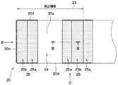
以上が本実施形態におけるモールドパッケージ1の基本的な構成である。そして、本実施形態では、搭載部10および端子部20は、モールド樹脂60で封止される封止領域に、それぞれ凹凸形状とされた凹凸領域が構成されている。まず、端子部20の凹凸領域について、図2〜図6を参照しつつ説明する。なお、以下では、端子部20のうちのモールド樹脂60にて封止される領域を封止領域23として説明する。
The above is the basic configuration of the mold package 1 in the present embodiment. Then, in the present embodiment, the mounting
端子部20は、図1および図2に示されるように、搭載部10側の領域が封止領域23となる。そして、端子部20は、図2に示されるように、一面20aのうちの封止領域23に、ボンディングワイヤ50と接続されるワイヤ領域24を有している。また、端子部20は、一面20aのうちの封止領域23において、ワイヤ領域24と異なる領域に凹凸形状とされた一面凹凸領域25を有している。なお、本実施形態では、ワイヤ領域24が接続領域に相当している。
As shown in FIGS. 1 and 2, the
具体的には、端子部20は、前側面20c側から後側面20e側に向かう方向を長手方向とする板状とされている。なお、図2中では、紙面左右方向が長手方向に相当する。そして、一面20aのうちの封止領域23では、長手方向に沿って、前側面20c側から一面凹凸領域25、ワイヤ領域24、一面凹凸領域25が順に位置している。つまり、一面20aのうちの封止領域23では、ワイヤ領域24を挟むように2つの一面凹凸領域25が位置している。
Specifically, the
一面凹凸領域25は、ワイヤ領域24側が第1凹凸領域25aとされ、第1凹凸領域25aを挟んでワイヤ領域24と反対側が第2凹凸領域25bとされている。なお、2つの一面凹凸領域25のうちの前側面20c側と反対側に位置する一面凹凸領域25は、第2凹凸領域25bを挟んでワイヤ領域24側と反対側にも第1凹凸領域25aを有している。そして、本実施形態では、一面20aのうちの封止領域23は、前側面20c側から、前側面20c側と反対側に位置する一面凹凸領域25のうちの第2凹凸領域25bまでとされている。つまり、前側面20c側から最も離れた第1凹凸領域25aは、封止領域23外に位置している。但し、封止領域23は、前側面20c側と反対側に位置する一面凹凸領域25が全て含まれていてもよい。
In the one-sided concavo-
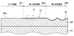
第1凹凸領域25aは、図3および図4に示されるように、金属薄膜22上に複数の金属粒子70が積層されて構成される微小凹凸部71を有する凹凸形状とされている。具体的には、本実施形態では、図4に示されるように、微小凹凸部71は、金属薄膜22側から当該金属薄膜22と反対側に向かって先細り形状となるように複数の金属粒子70が積層されることで構成されている。つまり、本実施形態では、微小凹凸部71は、複数の金属粒子70が凸状に積層されることで構成されている。そして、微小凹凸部71は、隣接する金属粒子70の間に空隙72が形成された状態となっている。
As shown in FIGS. 3 and 4, the first
空隙72は、隣接する金属粒子70の間の空間が互いに繋がる状態で構成されていると共に、金属粒子70が積層されている領域よりも外側の空間と繋がる状態で構成されている。本実施形態では、金属粒子70が凸状に積層されるため、空隙72は、例えば、隣接する凸部の間に構成される凹部と繋がっているともいえる。そして、空隙72は、一面20aと直交する方向の断面の大きさが数nm〜100nm程度とされている。ここで、本実施形態では、モールド樹脂60は、エポキシ樹脂で構成されており、溶融状態で分子の末端間距離が3〜10nm程度となる。このため、金属粒子70は、モールド樹脂60を構成する溶融樹脂が侵入可能な空隙72が形成されるように積層されているともいえる。そして、特に図示しないが、空隙72内には、モールド樹脂60が入り込んだ状態となっている。また、本実施形態では、微小凹凸部71は、最大高さが300nm以下とされている。言い換えると、金属薄膜22から最も離れている部分と当該金属薄膜22との間の最大長さが300nm以下とされている。
The
なお、金属粒子70は、本実施形態では、金属薄膜22と同じ材料の酸化物で構成されている。つまり、本実施形態では、めっき膜がNiで構成されているため、Niの酸化物で構成される金属粒子70が積層されることで微小凹凸部71が構成されている。
The
第2凹凸領域25bは、図3に示されるように、金属薄膜22に数μm程度の溝部73が複数形成されていると共に、溝部73上を含む金属薄膜22上に上記微小凹凸部71が形成された凹凸形状とされている。つまり、第2凹凸領域25bは、第1凹凸領域25aには形成されていない溝部73が形成されており、第1凹凸領域25aよりも大きな高低差を有する凹凸形状とされている。
In the second concavo-
以上が端子部20の一面20aにおける構成である。なお、微小凹凸部71が形成されている領域は、上記のように、微小凹凸部71内に空隙72が形成されているため、多孔質領域となっているともいえる。
The above is the configuration of the one
端子部20の前側面20cは、図1に示されるように、全面が封止領域23となる。そして、図5に示されるように、前側面20cは、一面20a側の領域が前側面凹凸領域26とされている。つまり、前側面20cは、第2凹凸領域25bと連なる領域が前側面凹凸領域26とされている。なお、前側面凹凸領域26は、横側面20dと横側面20fとの間において、一面20aから最も離れた部分までの長さがほぼ等しくなっている。また、前側面凹凸領域26は、第1凹凸領域25aと同様の構成とされており、複数の金属粒子70が積層されることで構成される凹凸形状とされている。
As shown in FIG. 1, the entire
端子部20の横側面20d、20fは、図1に示されるように、搭載部10側の領域が封止領域23となる。そして、図6に示されるように、横側面20dは、封止領域23において、一面20a側に横側面凹凸領域27を有している。具体的には、横側面凹凸領域27は、横側面20dのうちの一面20a側の領域において、第1凹凸領域25aおよび第2凹凸領域25bと連なる領域に構成されている。また、横側面凹凸領域27は、第2凹凸領域25bと繋がる領域から当該第2凹凸領域25bから離れるほど、一面20aから最も離れた部分までの長さが短くなっている。すなわち、横側面凹凸領域27は、第1凹凸領域25aと繋がる領域では、当該第2凹凸領域25bから離れるほど、一面20aから最も離れた部分までの長さが短くなっている。
As shown in FIG. 1, the lateral side surfaces 20d and 20f of the
なお、横側面凹凸領域27は、第1凹凸領域25aと同様の構成とされており、複数の金属粒子70が積層されることで構成される凹凸形状とされている。また、横側面20dのうちの第1凹凸領域25aと繋がる領域とは、言い換えると、横側面20dのうちの第1凹凸領域25aの直下に位置する領域のことである。同様に、横側面20dのうちの第2凹凸領域25bと繋がる領域とは、言い換えると、横側面20dのうちの第2凹凸領域25bの直下に位置する領域のことである。また、特に図示しないが、横側面20fは、横側面20dと同様に、一面20a側に横側面凹凸領域27が構成されている。
The lateral side
以上が本実施形態における端子部20の構成である。なお、図2中の一面凹凸領域25、図5中の前側面凹凸領域26、図6中の横側面凹凸領域27には、理解をし易くするために、凹凸形状を示す複数の点を示してある。次に、搭載部10の構成について説明する。なお、以下では、搭載部10のうちのモールド樹脂60にて封止される領域を封止領域13として説明する。
The above is the configuration of the
搭載部10の一面10aは、図7に示されるように、略中央部が搭載領域14とされ、搭載領域14を囲む領域が凹凸形状とされた一面凹凸領域15とされている。なお、搭載領域14は、接合部材30を介して半導体チップ40が配置される領域のことである。そして、搭載部10の一面10aでは、図1に示されるように、一面凹凸領域15がモールド樹脂60で封止される封止領域13となる。
As shown in FIG. 7, the one
一面凹凸領域15は、搭載領域14側が第1凹凸領域15aとされ、第1凹凸領域15aを挟んで搭載領域14と反対側が第2凹凸領域15bとされている。第1凹凸領域15aは、端子部20の第1凹凸領域25aと同様に、複数の金属粒子70が積層されて微小凹凸部71が構成された凹凸形状とされている。また、第2凹凸領域15bは、端子部20の第2凹凸領域25bと同様に、溝部73が複数形成されていると共に、溝部73上を含む金属薄膜12上に上記微小凹凸部71が構成された凹凸形状とされている。
The one-sided concavo-
搭載部10の側面10c〜10fは、図1に示されるように、それぞれ全面が封止領域13となる。そして、側面10cは、図8に示されるように、一面20a側の領域が側面凹凸領域16とされている。側面凹凸領域16は、第1凹凸領域15aと同様に、複数の金属粒子70が積層されて微小凹凸部71が構成された凹凸形状とされている。また、側面凹凸領域16は、側面10dと側面10fとの間において、一面10aから最も離れた部分までの長さがほぼ等しくなっている。なお、特に図示しないが、他の側面10d、10e、10fにおいても、側面10cと同様に、一面10a側の領域が側面凹凸領域16とされている。また、図7中の一面凹凸領域15、および図8中の側面凹凸領域16には、理解をし易くするために、凹凸形状を示す複数の点を示してある。
As shown in FIG. 1, the entire side surfaces 10c to 10f of the mounting
以上が本実施形態におけるモールドパッケージ1の構成である。次に、本実施形態のモールドパッケージ1の製造方法について、図9および図10を参照しつつ説明する。 The above is the configuration of the mold package 1 in the present embodiment. Next, a method for manufacturing the mold package 1 of this embodiment will be described with reference to FIGS. 9 and 10.
まず、図9および図10に示されるように、搭載部10と端子部20とがタイバーや外周フレーム等で一体化されたリードフレーム80を用意する。なお、図9および図10では、リードフレーム80における1つの端子部20のみを図示している。また、本実施形態では、リードフレーム80が基礎部材に相当する。
First, as shown in FIGS. 9 and 10, a
そして、搭載部10に、一面凹凸領域15および側面凹凸領域16を形成する。また、端子部20に、一面凹凸領域25、前側面凹凸領域26、および横側面凹凸領域27を形成する。以下に、端子部20に一面凹凸領域25、前側面凹凸領域26、および横側面凹凸領域27を形成する工程について具体的に説明する。なお、搭載部10に一面凹凸領域15および側面凹凸領域16を形成する工程は、端子部20に一面凹凸領域25、前側面凹凸領域26、および横側面凹凸領域27を形成する工程と同様である。
Then, the one-sided concavo-
すなわち、本実施形態では、レーザ光Lを発振する光源および集光レンズ等を適宜配置し、端子部20の第2凹凸領域25bとなる領域にレーザ光Lを照射する。本実施形態では、例えば、第2凹凸領域25bにレーザ光Lを照射する場合、図9中の矢印Aで示されるように、端子部20の長手方向と直交する方向に沿った複数個所にレーザ光Lを照射する。この際、例えば、端子部20を搭載したテーブルを走査すること、または光源を走査することにより、光源を第2凹凸領域25bに対して相対移動させ、矢印Aに沿った複数の位置にレーザ光Lを照射する。なお、光源側にミラーを配置し、当該ミラーを回転動作さることでレーザ光Lを走査させる、いわゆるガルバノスキャナを用いてレーザ光Lを照射するようにしてもよい。
That is, in the present embodiment, a light source that oscillates the laser light L, a condenser lens, and the like are appropriately arranged, and the laser light L is applied to the area of the
この場合、図10に示されるように、レーザ光Lが照射された領域では、金属粒子70が浮遊して数μm程度の溝部73が形成される。そして、浮遊した金属粒子70は、レーザ光Lが照射された領域の周囲に蒸着する。これにより、浮遊した金属粒子70が積層されて微小凹凸部71が構成される。この際、浮遊した金属粒子70は、レーザ光Lが照射された領域の周囲の領域にも蒸着する。このため、一面20aでは、第2凹凸領域25bと隣接する位置に複数の金属粒子70が積層されて第1凹凸領域25aが構成される。また、前側面20c、横側面20d、および横側面20fでは、第2凹凸領域25bと隣接する一面20a側に複数の金属粒子70が積層され、前側面凹凸領域26、横側面凹凸領域27が構成される。このように前側面20cおよび横側面20d、20fに凹凸形状を構成することにより、各側面20c、20d、20fに対して特別な処理を行う必要もなく、製造工程の簡略化を図ることもできる。
In this case, as shown in FIG. 10, in the region irradiated with the laser beam L, the
なお、金属粒子70は、上記のように、空隙72が構成されるように積層される。また、横側面20d、20fでは、第2凹凸領域25bから離れるほど金属粒子70が付着し難くなる。このため、図6に示されるように、横側面凹凸領域27は、第2凹凸領域25bから離れるほど、一面20aから最も離れた部分までの長さが短くなる。
The
また、レーザ光Lを照射する場合は、金属粒子70が飛散して製造装置に付着する等し、当該製造装置が汚染されないような条件で行われることが好ましい。例えば、本実施形態のようにNiめっき膜で金属薄膜22を構成する場合は、エネルギー密度が300J/cm2以下であって、パルス幅が1μm秒以下であり、金属薄膜22の表面温度が1500℃程度となるようにレーザ光Lを照射すればよい。
Further, when the laser light L is irradiated, it is preferable that the
また、本実施形態では、金属薄膜22がNiめっき膜で構成されているため、上記条件でレーザ光Lを照射すると、金属粒子70は、図4に示されるように、金属薄膜22側から当該金属薄膜22と反対側に向かって先細り形状となるように蒸着する。これについては、明確な原理が明らかではないが、浮遊した金属粒子70が蒸着した際、当該金属粒子70が有するエネルギーが小さいために再配列し難いためであると推測される。
In addition, in the present embodiment, since the metal
以上のようにして端子部20には、一面凹凸領域25、前側面凹凸領域26および横側面凹凸領域27が形成される。
As described above, the one-sided concavo-
また、特に図示しないが、搭載部10においても、第2凹凸領域15bにレーザ光Lを照射する。これにより、第2凹凸領域15bは、溝部73が形成されると共に金属粒子70が積層されて凹凸形状が構成される。また、一面10aにおける第2凹凸領域15bの周囲は、金属粒子70が積層されることで第1凹凸領域15aが構成される。また、側面10c〜10fは、第2凹凸領域15bと隣接する一面10a側の領域に、金属粒子70が積層されて側面凹凸領域16が構成される。
Although not shown in the drawing, the laser light L is also applied to the second concavo-convex region 15b in the mounting
次に、搭載部10の搭載領域14に接合部材30を介して半導体チップ40を搭載する。そして、ワイヤボンディングを行い、半導体チップ40と端子部20とを接合する。なお、端子部20には、ワイヤ領域24に対してワイヤボンディングを行う。
Next, the
続いて、上記工程を行ったものを図示しない金型内に配置し、金型内にモールド樹脂60を構成する溶融樹脂を流し込んで固化する。この際、溶融樹脂は、空隙72が当該溶融樹脂が入り込める大きさとされているため、空隙72にも入り込んだ状態で固化される。その後、適宜外周フレーム等を除去することにより、上記モールドパッケージが構成される。
Subsequently, the product obtained through the above steps is placed in a mold (not shown), and the molten resin forming the
以上説明したように、本実施形態では、搭載部10は、一面10aに一面凹凸領域15が構成されていると共に、側面10c〜10fにも側面凹凸領域16が構成されている。このため、搭載部10の側面10c〜10fからモールド樹脂60が剥離することを抑制できる。同様に、端子部20は、一面20aに一面凹凸領域25が構成されていると共に、側面20c、20d、20fにも側面凹凸領域26、27が構成されている。このため、端子部20の側面20c、20d、20fからモールド樹脂60が剥離することを抑制できる。
As described above, in the present embodiment, the mounting
また、隣接する金属粒子70の間には、空隙72が形成されている。そして、モールド樹脂60は、空隙72内にも入り込んだ状態となっている。このため、空隙72が形成されていない場合と比較して、搭載部10および端子部20と、モールド樹脂60との密着性を向上できる。このため、さらにモールド樹脂60が剥離することを抑制でき、ひいては気密性を向上できる。
A void 72 is formed between the
(第2実施形態)
第2実施形態について説明する。本実施形態は、第1実施形態に対して、端子部20のワイヤ領域24にも凹凸形状が構成されたものであり、その他に関しては上記第1実施形態と同様であるため、ここでは説明を省略する。
(Second embodiment)
The second embodiment will be described. The present embodiment is different from the first embodiment in that the
本実施形態では、図11に示されるように、端子部20は、ワイヤ領域24が第1凹凸領域25aとされ、当該ワイヤ領域24が2つの第2凹凸領域25bで挟まれた状態とされている。つまり、本実施形態では、端子部20の一面20aは、封止領域23において全て一面凹凸領域25とされている。なお、図11中の一面凹凸領域25には、理解をし易くするために、凹凸形状を示す複数の点を示してある。
In the present embodiment, as shown in FIG. 11, in the
これによれば、ワイヤ領域24は、実際にボンディングワイヤ50が接続される領域の周囲も凹凸形状とされる。このため、ワイヤ領域24とモールド樹脂60との密着性を向上できる。
According to this, the
また、ワイヤ領域24に対してワイヤボンディングを行う場合は、例えば、ワイヤ領域24にワイヤを押し当てた状態で超音波振動を印加することによって行われる。ここで、本発明者らは、ワイヤボンディングを行う場合、凹凸の高低差が300nm以下の場合には、ワイヤボンディングを行う際の接合性が低下しないことを見出している。そして、第1凹凸領域25aは、最大高さが300nm以下とされた微小凹凸部71で構成される。このため、本実施形態では、ボンディングワイヤ50との接合性が低下することを抑制しつつ、さらにモールド樹脂60との密着性を向上できる。
Further, when wire bonding is performed on the
なお、このようにワイヤ領域24を第1凹凸領域25aとする場合には、第2凹凸領域25bから浮遊させた金属粒子70がワイヤ領域24に蒸着するようにすればよい。言い換えると、ワイヤ領域24に金属粒子70が蒸着するように、第2凹凸領域25bから金属粒子70を浮遊させればよい。
When the
また、特に図示しないが、本実施形態では、第2凹凸領域25bがワイヤ領域24と隣接して位置している。このため、横側面20d、20fは、一面20a側の領域のうちのワイヤ領域24と繋がる部分にも横側面凹凸領域27が構成される。
Further, although not particularly shown, in the present embodiment, the second
(第3実施形態)
第3実施形態について説明する。本実施形態は、第1実施形態に対して、端子部20に第2凹凸領域25bが形成されていないものであり、その他に関しては、第1実施形態と同様であるため、ここでは説明を省略する。
(Third Embodiment)
A third embodiment will be described. The present embodiment is different from the first embodiment in that the second concavo-
本実施形態では、図12に示されるように、端子部20は、一面20aのうちの封止領域23において、ワイヤ領域24と異なる領域が第1凹凸領域25aとされており、第2凹凸領域25bが形成されていない。また、特に図示しないが、前側面20cは、全領域が前側面凹凸領域26とされている。同様に、横側面20d、20fは、封止領域23となる全領域が横側面凹凸領域27とされている。
In the present embodiment, as shown in FIG. 12, in the
さらに、特に図示しないが、搭載部10は、一面10aのうちの封止領域23において、搭載領域14と異なる全領域が第1凹凸領域15aとされており、第2凹凸領域25bが形成されていない。また、特に図示しないが、各側面10c〜10fは、全領域が側面凹凸領域16とされている。
Further, although not particularly shown, in the mounting
次に、このような端子部20の製造方法について説明する。なお、搭載部10の製造方法についても同様である。
Next, a method of manufacturing such a
本実施形態では、図13に示されるように、搭載部10と端子部20とがタイバーや外周フレーム等で一体化されたリードフレーム80を用意する。そして、搭載部10のうちのワイヤ領域24上に図示しないマスクを配置する。次に、端子部20のうちの金属粒子70を積層させたい領域の近傍にターゲット部材90を配置する。なお、本実施形態では、ターゲット部材90として、Niで構成されたものを用いる。
In this embodiment, as shown in FIG. 13, a
そして、ターゲット部材90にレーザ光Lを照射し、ターゲット部材90から金属粒子70を浮遊させて端子部20に蒸着させて積層する。これにより、端子部20に金属粒子70が積層されて第1凹凸領域25aが構成される。その後、ワイヤ領域24に形成されたマスクを除去する。これにより、端子部20の一面20aでは、ワイヤ領域24と異なる領域に第1凹凸領域25aが構成された状態となる。
Then, the
また、端子部20の側面20c、20d、20fでは、横側面凹凸領域26、27がそれぞれ形成される。この際、ターゲット部材90を移動させる等することにより、側面20c、20d、20fの所望箇所に金属粒子70を積層できる。つまり、本実施形態では、ターゲット部材90を移動させる等することにより、側面20c、20d、20fの全領域に金属粒子70を積層して凹凸形状を構成する。
Further, on the side surfaces 20c, 20d, 20f of the
なお、ターゲット部材90にレーザ光Lを照射した場合、例えば、エネルギー密度が10J/cm2であり、パルス幅を1μm秒以下で照射すると、ターゲット部材90から金属粒子70が0.25mm程度の高さまで浮遊する。このため、ターゲット部材90と端子部20との間隔を0.25mm以下とすることにより、ターゲット部材90から金属粒子70を端子部20に蒸着させて積層することができる。
When the
また、ターゲット部材90に照射するレーザ光Lのエネルギー密度等を大きくすれば、ターゲット部材90から浮遊する金属粒子70の浮遊距離は長くなる。このため、ターゲット部材90から端子部20に金属粒子70が蒸着するのであれば、レーザ光Lのエネルギー密度や、ターゲット部材90と端子部20との間隔は適宜変更可能である。但し、上記のように、レーザ光Lのエネルギー密度を大きくし過ぎると、ターゲット部材90から金属粒子が飛散する可能性があるため、レーザ光Lのエネルギー密度は、300J/cm2以下とすることが好ましい。
Further, if the energy density of the laser light L with which the
また、特に図示しないが、搭載部10においても、ターゲット部材90から金属粒子70を浮遊させて当該搭載部10に金属粒子70を蒸着させる。なお、搭載部10は、例えば、搭載領域14上にマスクを配置し、金属粒子70を蒸着した後にマスクを除去することにより、搭載領域14に金属粒子70が蒸着していない構成とできる。
Further, although not particularly shown, also in the mounting
以上説明した本実施形態によれば、ターゲット部材90から金属粒子70を浮遊させて凹凸形状を構成するため、所望箇所に凹凸形状を構成できる。例えば、端子部20の側面20c、20d、20fにおける他面20b側にも凹凸形状を構成できる。したがって、モールド樹脂60との密着性をさらに向上できる。
According to the present embodiment described above, since the
なお、上記では、端子部20は、前側面20cの全領域が前側面凹凸領域26とされ、横側面20d、20fの封止領域23となる全領域が横側面凹凸領域27とされている例について説明した。しかしながら、端子部20は、例えば、前側面20cの一面20a側のみが前側面凹凸領域26とされ、横側面20d、20fの封止領域23となる一面20a側のみが横側面凹凸領域27とされていてもよい。つまり、本実施形態では、ターゲット部材90から金属粒子70を浮遊させて凹凸形状を構成するため、所望箇所に凹凸形状を構成でき、凹凸形状が構成される範囲は適宜変更可能である。
In the above, in the
(第3実施形態の変形例)
第3実施形態の変形例について説明する。第3実施形態において、端子部20のワイヤ領域24にマスクを形成せず、図14に示されるように、ワイヤ領域24も第1凹凸領域25aとされていてもよい。つまり、端子部20は、封止領域23における一面20aの全領域が第1凹凸領域25aとされていてもよい。このような構成としても、第1凹凸領域25aは、最大高さが300nm以下とされた微小凹凸部71で構成されるため、モールド樹脂60との密着性を向上しつつ、ボンディングワイヤ50との接合性が低下することを抑制できる。
(Modification of Third Embodiment)
A modified example of the third embodiment will be described. In the third embodiment, a mask may not be formed on the
(第4実施形態)
第4実施形態について説明する。本実施形態は、第3実施形態に対して、金属粒子70の積層状態を変更したものであり、その他に関しては、第3実施形態と同様であるため、ここでは説明を省略する。
(Fourth Embodiment)
A fourth embodiment will be described. In this embodiment, the stacked state of the
本実施形態では、端子部20は、Al、またはAl合金で構成される主金属部21で構成され、金属薄膜22が備えられていない。そして、本実施形態では、第1凹凸領域25aは、Alの酸化物で構成される金属粒子70が積層された微小凹凸部71を有する凹凸形状とされている。なお、本実施形態では、端子部20は、金属薄膜22が備えられていないため、各面20a〜20fは主金属部21で構成されている。
In this embodiment, the
本実施形態の微小凹凸部71は、図15に示されるように、複数の金属粒子70が積層されることで構成されているが、複数の金属粒子70が略層状に配列されている。つまり、本実施形態では、複数の金属粒子70は、上記図4で説明した金属粒子70より規則的に配列されている。なお、本実施形態の微小凹凸部71は、金属薄膜22側と反対側に位置する金属粒子70の配列に起因した凹凸形状にて構成される。また、本実施形態においても、微小凹凸部71は、最大高さが300nm以下とされている。
The fine concavo-
そして、微小凹凸部71には、内部に隣接する金属粒子70の間に空隙72が形成されている。なお、この空隙72は、上記第1実施形態と同様に、モールド樹脂60を構成する溶融樹脂が侵入可能な大きさとされている。そして、空隙72には、モールド樹脂60が入り込んだ状態となる。
Then, in the minute concavo-
また、第2凹凸領域25bは、溝部73上を含む金属薄膜22上に、上記略層状の微小凹凸部71が形成された凹凸形状とされている。そして、前側面凹凸領域26、および横側面凹凸領域27は、第1凹凸領域25aと同様に、上記略層状の微小凹凸部71が形成された凹凸形状とされている。
The
同様に、搭載部10は、Al、またはAl合金で構成される主金属部11で構成され、金属薄膜12が備えられていない。そして、第1凹凸領域15aは、端子部20の第1凹凸領域25aと同様の構成とされ、上記略層状の微小凹凸部71が形成された凹凸形状とされている。また、第2凹凸領域15bは、溝部73上を含む金属薄膜12上に、上記略層状の微小凹凸部71が形成された凹凸形状とされている。そして、側面凹凸領域16は、第1凹凸領域25aと同様に、上記略層状の微小凹凸部71が形成された凹凸形状とされている。なお、本実施形態では、搭載部10は、金属薄膜12が備えられていないため、各面10a〜10fは主金属部11で構成されている。
Similarly, the mounting
このような凹凸形状は、上記第1実施形態と同様の条件でレーザ光Lを照射することにより形成される。なお、これについても明確な原理が明らかではないが、次のように推測される。すなわち、主金属部11、12をAlまたはAl合金で構成してレーザ光が照射されるようにすると、金属薄膜22をNiめっき膜で構成してレーザ光が照射されるようにした場合より、AlまたはAl合金の融点がNiより低いため、浮遊した金属粒子70がより大きなエネルギーを有することになる。このため、上記第1実施形態と同様の条件でレーザ光Lを照射すると、浮遊した金属粒子70が蒸着した際に当該金属粒子70が固定化するまでに失えるエネルギーが大きくなり、金属粒子70が蒸着した後に規則正しく配列することが可能であるためと推測される。
Such a concavo-convex shape is formed by irradiating the laser beam L under the same conditions as in the first embodiment. The clear principle of this is not clear, but it is presumed as follows. That is, when the
以上説明したように、凹凸形状は、金属粒子70が積層されて略層状とされていてもよい。また、このような凹凸形状は、上記第1実施形態の凹凸形状よりも空隙72が占める割合が大きくなり、モールド樹脂60の空隙72内に入り込む量が多くなる。このため、さらに搭載部10および端子部20と、モールド樹脂60との密着性を向上できる。
As described above, the concavo-convex shape may be substantially layered by laminating the
(他の実施形態)
本発明は上記した実施形態に限定されるものではなく、特許請求の範囲に記載した範囲内において適宜変更が可能である。
(Other embodiments)
The present invention is not limited to the above-described embodiments, but can be appropriately modified within the scope of the claims.
例えば、上記各実施形態において、モールド樹脂60は、エポキシ樹脂中に、線膨張係数を調整するためのアルミナやシリカ等のフィラーが混入されていてもよい。
For example, in each of the above-described embodiments, the
また、上記各実施形態において、ボンディングワイヤ50としてAuワイヤやCuワイヤを用いる場合、ボンディングワイヤ50との接合性を向上させるため、金属薄膜22は、めっき膜上にAgめっき膜が積層されていてもよい。つまり、ボンディングワイヤ50を構成する材料と接合性が高い接合用めっき膜が積層されていてもよい。この場合は、接合用めっき膜上に金属粒子70が積層されて凹凸形状が構成される。
Further, in each of the above-described embodiments, when an Au wire or a Cu wire is used as the
さらに、上記第3実施形態において、ターゲット部材90は、金属薄膜22と異なる金属材料を用いて構成してもよく、例えば、Fe、Al、またはSn等で構成されていてもよい。このようなターゲット部材90を用いたとしても、搭載部10および端子部20の所望箇所に金属粒子70を積層して凹凸形状を構成できる。つまり、上記第3実施形態では、ターゲット部材90として金属薄膜22を構成する材料と異なる材料で構成されるものも用いることができ、設計の自由度を向上できる。言い換えると、上記第3実施形態では、使用用途に応じて積層する金属粒子70を適宜変更でき、設計の自由度を向上できる。なお、例えば、上記第3実施形態において、ターゲット部材90をAlまたはAl合金で構成した場合には、上記第3実施形態と同様の条件でレーザ光Lを照射することにより、上記第4実施形態のように、複数の金属粒子70が略層状に配列されて積層される。
Furthermore, in the third embodiment, the
また、上記第3実施形態において、基材として樹脂で構成されるフレキシブル基板を用い、当該フレキシブル基板の所望領域に金属粒子70を積層して凹凸形状を構成するようにしてもよい。
Further, in the third embodiment, a flexible substrate made of resin may be used as the base material, and the
また、上記第1、第2、第4実施形態において、溝部73が形成されると共に金属粒子70が浮遊し、浮遊した当該金属粒子70が蒸着して積層されるのであれば、レーザ光L以外を照射するようにしてもよい。例えば、スパッタの原理を適用し、金属粒子を衝突させるようにしてもよい。同様に、上記第3実施形態においても、ターゲット部材90に金属粒子を衝突させて当該ターゲット部材90から金属粒子70を浮遊させるようにしてもよい。
In addition, in the first, second, and fourth embodiments, other than the laser light L as long as the
10 搭載部(基材)
10a 一面
10c〜10f 側面
13 封止領域
15 一面凹凸領域
16 側面凹凸領域
20 接続部(基材)
20a 一面
20c〜20f 側面
23 封止領域
26、27 側面凹凸領域
10 Mounting part (base material)
10a One
20a One
Claims (15)
前記一面のうちの前記封止領域を構成する領域には、凹凸形状とされた一面凹凸領域(15、25)が構成され、
前記側面のうちの前記封止領域を構成する領域には、凹凸形状とされた側面凹凸領域(16、26、27)が構成され、
前記一面凹凸領域および前記側面凹凸領域は、複数の金属粒子(70)が積層されることで構成されており、
前記一面は、前記封止領域を構成する領域に接続部材(50)と接続される接続領域(24)を有し、
前記一面凹凸領域は、前記接続領域と異なる領域に構成されており、前記接続領域側に構成された第1凹凸領域(25a)と、前記第1凹凸領域を挟んで前記接続領域と反対側に構成された第2凹凸領域(25b)と、を有し、
前記第1凹凸領域は、前記複数の金属粒子が積層されることで構成され、
前記第2凹凸領域は、溝部(73)が形成されていると共に、前記溝部を含む領域に前記複数の金属粒子が積層されることで構成され、前記第1凹凸領域よりも凹凸の高低差が大きくされている基材。 A sealing region (13, having a surface (10a, 20a) and side surfaces (10c to 10f, 20c, 20d, 20f) continuous with the surface, and the surface and the side surface being sealed with a mold resin (60). 23) In the base material,
One surface concavo-convex region (15, 25) having a concavo-convex shape is formed in a region of the one surface that constitutes the sealing region,
In the area of the side surface forming the sealing area, side surface uneven areas (16, 26, 27) having an uneven shape are formed,
The one-sided concavo-convex region and the side-face concavo-convex region are formed by laminating a plurality of metal particles (70) ,
The one surface has a connection region (24) connected to a connection member (50) in a region forming the sealing region,
The one-sided concavo-convex region is formed in a region different from the connection region, and on the opposite side of the connection region from the first concavo-convex region (25a) formed on the connection region side and the first concavo-convex region. And a second uneven region (25b) configured,
The first uneven region is formed by stacking the plurality of metal particles,
The second concavo-convex region is formed by forming a groove (73) and laminating the plurality of metal particles in a region including the groove, and the difference in height of concavo-convex is higher than that of the first concavo-convex region. The base material being made larger .
前記一面のうちの前記封止領域を構成する領域には、凹凸形状とされた一面凹凸領域(15、25)が構成され、
前記側面のうちの前記封止領域を構成する領域には、凹凸形状とされた側面凹凸領域(16、26、27)が構成され、
前記一面凹凸領域および前記側面凹凸領域は、複数の金属粒子(70)が積層されることで構成されており、
前記一面は、前記封止領域を構成する領域に接続部材(50)と接続される接続領域(24)を有し、
前記一面凹凸領域は、前記接続領域を含む領域に構成された第1凹凸領域(25a)と、前記第1凹凸領域と異なる領域に構成された第2凹凸領域(25b)と、を有し、
前記第1凹凸領域は、前記複数の金属粒子が積層されることで構成され、
前記第2凹凸領域は、溝部(73)が形成されていると共に、前記溝部を含む領域に前記複数の金属粒子が積層されることで構成され、前記第1凹凸領域よりも凹凸の高低差が大きくされている基材。 A sealing region (13, having a surface (10a, 20a) and side surfaces (10c to 10f, 20c, 20d, 20f) continuous with the surface, and the surface and the side surface being sealed with a mold resin (60). 23) In the base material,
One surface concavo-convex region (15, 25) having a concavo-convex shape is formed in a region of the one surface that constitutes the sealing region,
In the area of the side surface forming the sealing area, side surface uneven areas (16, 26, 27) having an uneven shape are formed,
The one-sided concavo-convex region and the side-face concavo-convex region are formed by laminating a plurality of metal particles (70) ,
The one surface has a connection region (24) connected to a connection member (50) in a region forming the sealing region,
The one-sided concavo-convex region has a first concavo-convex region (25a) configured in a region including the connection region and a second concavo-convex region (25b) configured in a region different from the first concavo-convex region,
The first uneven region is formed by stacking the plurality of metal particles,
The second concavo-convex region is formed by forming a groove (73) and laminating the plurality of metal particles in a region including the groove, and the difference in height of concavo-convex is higher than that of the first concavo-convex region. The base material being made larger .
前記空隙は、互いに繋がっていると共に前記金属粒子が積層されている領域よりも外側の空間と繋がっている請求項1または2に記載の基材。 The plurality of metal particles are stacked with a gap (72) formed between the adjacent metal particles,
The base material according to claim 1 or 2 , wherein the voids are connected to each other and are connected to a space outside an area where the metal particles are stacked.
一面(10a)および前記一面と連なる側面(10c〜10f)を有する前記搭載部と、
一面(20a)および前記一面と連なる側面(20c、20d、20f)を有する前記端子部と、
前記搭載部の一面に搭載される半導体チップ(40)と、
前記半導体チップと前記端子部とを電気的に接続する接続部材(50)と、
前記半導体チップおよび前記接続部材を封止しつつ、前記搭載部の前記一面および前記側面、前記端子部の前記一面および前記側面を封止する前記モールド樹脂と、を備え、
前記搭載部および前記端子部は、前記モールド樹脂で封止される封止領域(13、23)において、前記一面に凹凸形状とされた一面凹凸領域(15、25)が構成され、前記側面に凹凸形状とされた側面凹凸領域(16、26、27)が構成され、
前記一面凹凸領域および前記側面凹凸領域は、複数の金属粒子(70)が積層されることで構成されており、
前記一面は、前記封止領域を構成する領域に接続部材(50)と接続される接続領域(24)を有し、
前記一面凹凸領域は、前記接続領域と異なる領域に構成されており、前記接続領域側に構成された第1凹凸領域(25a)と、前記第1凹凸領域を挟んで前記接続領域と反対側に構成された第2凹凸領域(25b)と、を有し、
前記第1凹凸領域は、前記複数の金属粒子が積層されることで構成され、
前記第2凹凸領域は、溝部(73)が形成されていると共に、前記溝部を含む領域に前記複数の金属粒子が積層されることで構成され、前記第1凹凸領域よりも凹凸の高低差が大きくされているモールドパッケージ。 In the mold package in which the mounting portion (10) and the terminal portion (20) are sealed with the molding resin (60),
The mounting portion having one surface (10a) and side surfaces (10c to 10f) continuous with the one surface;
The terminal portion having one surface (20a) and side surfaces (20c, 20d, 20f) continuous with the one surface;
A semiconductor chip (40) mounted on one surface of the mounting portion;
A connection member (50) for electrically connecting the semiconductor chip and the terminal portion,
While sealing the semiconductor chip and the connection member, the one surface and the side surface of the mounting portion, the mold resin that seals the one surface and the side surface of the terminal portion,
In the sealing area (13, 23) sealed with the mold resin, the mounting portion and the terminal portion have one-sided uneven areas (15, 25) having an uneven shape on the one surface, and are formed on the side surface. Side surface uneven areas (16, 26, 27) having an uneven shape are formed,
The one-sided concavo-convex region and the side-face concavo-convex region are formed by laminating a plurality of metal particles (70) ,
The one surface has a connection region (24) connected to a connection member (50) in a region forming the sealing region,
The one-sided concavo-convex region is formed in a region different from the connection region, and on the opposite side of the connection region from the first concavo-convex region (25a) formed on the connection region side and the first concavo-convex region. And a second uneven region (25b) configured,
The first uneven region is configured by stacking the plurality of metal particles,
The second concavo-convex region is formed by forming a groove (73) and laminating the plurality of metal particles in a region including the groove, and the difference in height of concavo-convex is higher than that of the first concavo-convex region. Larger mold package.
一面(10a)および前記一面と連なる側面(10c〜10f)を有する前記搭載部と、
一面(20a)および前記一面と連なる側面(20c、20d、20f)を有する前記端子部と、
前記搭載部の一面に搭載される半導体チップ(40)と、
前記半導体チップと前記端子部とを電気的に接続する接続部材(50)と、
前記半導体チップおよび前記接続部材を封止しつつ、前記搭載部の前記一面および前記側面、前記端子部の前記一面および前記側面を封止する前記モールド樹脂と、を備え、
前記搭載部および前記端子部は、前記モールド樹脂で封止される封止領域(13、23)において、前記一面に凹凸形状とされた一面凹凸領域(15、25)が構成され、前記側面に凹凸形状とされた側面凹凸領域(16、26、27)が構成され、
前記一面凹凸領域および前記側面凹凸領域は、複数の金属粒子(70)が積層されることで構成されており、
前記一面は、前記封止領域を構成する領域に接続部材(50)と接続される接続領域(24)を有し、
前記一面凹凸領域は、前記接続領域を含む領域に構成された第1凹凸領域(25a)と、前記第1凹凸領域と異なる領域に構成された第2凹凸領域(25b)と、を有し、
前記第1凹凸領域は、前記複数の金属粒子が積層されることで構成され、
前記第2凹凸領域は、溝部(73)が形成されていると共に、前記溝部を含む領域に前記複数の金属粒子が積層されることで構成され、前記第1凹凸領域よりも凹凸の高低差が大きくされているモールドパッケージ。 In the mold package in which the mounting portion (10) and the terminal portion (20) are sealed with the molding resin (60),
The mounting portion having one surface (10a) and side surfaces (10c to 10f) continuous with the one surface;
The terminal portion having one surface (20a) and side surfaces (20c, 20d, 20f) continuous with the one surface;
A semiconductor chip (40) mounted on one surface of the mounting portion;
A connection member (50) for electrically connecting the semiconductor chip and the terminal portion,
While sealing the semiconductor chip and the connection member, the one surface and the side surface of the mounting portion, the mold resin that seals the one surface and the side surface of the terminal portion,
In the sealing area (13, 23) sealed with the mold resin, the mounting portion and the terminal portion have one-sided uneven areas (15, 25) having an uneven shape on the one surface, and are formed on the side surface. Side surface uneven areas (16, 26, 27) having an uneven shape are formed,
The one-sided concavo-convex region and the side-face concavo-convex region are formed by laminating a plurality of metal particles (70) ,
The one surface has a connection region (24) connected to a connection member (50) in a region forming the sealing region,
The one-sided concavo-convex region has a first concavo-convex region (25a) configured in a region including the connection region and a second concavo-convex region (25b) configured in a region different from the first concavo-convex region,
The first uneven region is formed by stacking the plurality of metal particles,
The second concavo-convex region is formed by forming a groove (73) and laminating the plurality of metal particles in a region including the groove, and the difference in height of concavo-convex is higher than that of the first concavo-convex region. Larger mold package.
前記モールド樹脂は、前記空隙内に入り込んでいる請求項6または7に記載のモールドパッケージ。 The plurality of metal particles are stacked with a gap (72) formed between the adjacent metal particles,
The mold package according to claim 6 or 7 , wherein the mold resin has entered the void.
前記一面および前記側面を有し、金属材料で構成された基礎部材(80)を用意することと、
前記一面のうちの前記封止領域を構成する領域に、凹凸形状とされた一面凹凸領域(15、25)を形成することと、
前記側面のうちの前記封止領域を構成する領域に、凹凸形状とされた側面凹凸領域(16、26、27)を形成することと、を行い、
前記一面凹凸領域を形成すること、および前記側面凹凸領域を形成することでは、前記一面に、溝部(73)を形成することで金属粒子(70)を浮遊させ、浮遊した前記金属粒子を、前記一面のうちの前記溝部、および前記溝部の周囲に蒸着して当該金属粒子を積層すると共に、前記側面に蒸着して当該金属粒子を積層することにより、前記一面凹凸領域および前記側面凹凸領域を形成する基材の製造方法。 A sealing region (13, having a surface (10a, 20a) and side surfaces (10c to 10f, 20c, 20d, 20f) continuous with the surface, and the surface and the side surface being sealed with a mold resin (60). 23) In the method for producing a substrate as described above,
Providing a base member (80) having the one surface and the side surface and made of a metal material;
Forming a one-sided concavo-convex region (15, 25) having a concavo-convex shape in a region of the one surface that constitutes the sealing region;
Forming side surface uneven areas (16, 26, 27) having an uneven shape in an area of the side surface that constitutes the sealing area,
By forming the one-sided unevenness region and forming the side-faced unevenness region, a metal particle (70) is suspended by forming a groove (73) on the one surface, and the suspended metal particle is Forming the one-sided concavo-convex region and the side-side concavo-convex region by vapor-depositing the metal particles on one side of the groove and the periphery of the groove and laminating the metal particles by vapor-depositing on the side surface. A method of manufacturing a substrate.
前記一面凹凸領域を形成することでは、前記一面のうちの前記接続領域と異なる領域に前記溝部を形成し、かつ、前記接続領域と異なる領域に前記金属粒子を蒸着して積層する請求項9に記載の基材の製造方法。 By preparing the base member, a member having a connection region (24) connected to the connection member (50) is prepared on the one surface,
Said By forming the one surface irregular region, the forming the groove in the connection region and different areas of said one surface, and, in claim 9 for laminating and depositing the metal particles in a region different from the connecting region A method for producing the described base material.
前記一面凹凸領域を形成することでは、前記一面のうちの前記接続領域と異なる領域に前記溝部を形成し、かつ、前記接続領域を含む領域に前記金属粒子を蒸着して積層する請求項9に記載の基材の製造方法。 By preparing the base member, a member having a connection area connected to the connection member (50) is prepared on the one surface,
Said By forming the one surface irregular region, the forming the groove in the connection region and different areas of said one surface, and, in claim 9 for laminating and depositing the metal particles in the region including the connection region A method for producing the described base material.
前記一面および前記側面を有する基礎部材(80)を用意することと、
前記一面のうちの前記封止領域を構成する領域に、凹凸形状とされた一面凹凸領域(15、25)を形成することと、
前記側面のうちの前記封止領域を構成する領域に、凹凸形状とされた側面凹凸領域(16、26、27)を形成することと、を行い、
前記一面凹凸領域を形成すること、および前記側面凹凸領域を形成することでは、金属材料で構成されるターゲット部材(90)を用意することと、前記ターゲット部材から金属粒子(70)を浮遊させ、浮遊した前記金属粒子を前記一面および前記側面に蒸着して積層することにより、前記一面凹凸領域および前記側面凹凸領域を形成することと、を行う基材の製造方法。 A sealing region (13, having a surface (10a, 20a) and side surfaces (10c to 10f, 20c, 20d, 20f) continuous with the surface, and the surface and the side surface being sealed with a mold resin (60). 23) In the method for producing a substrate as described above,
Providing a base member (80) having the one side and the side;
Forming a one-sided concavo-convex region (15, 25) having a concavo-convex shape in a region of the one surface that constitutes the sealing region;
Forming side surface uneven areas (16, 26, 27) having an uneven shape in an area of the side surface that constitutes the sealing area,
Forming the one-sided concavo-convex region and forming the side-face concavo-convex region prepares a target member (90) made of a metal material, and suspends metal particles (70) from the target member, A method of manufacturing a base material, comprising forming the one-sided concavo-convex region and the side-side concavo-convex region by depositing and laminating the floating metal particles on the one side and the side face.
前記一面凹凸領域を形成することでは、前記一面のうちの前記接続領域を含む領域に前記金属粒子を蒸着して積層する請求項12に記載の基材の製造方法。 By preparing the base member, a member having a connection area connected to the connection member (50) is prepared on the one surface,
Said By forming the one surface irregular region, method for producing a substrate according to claim 1 2 to be stacked by depositing the metallic particles in the region including the connection area of said one surface.
前記基材の一面および側面が封止されるように、前記モールド樹脂を形成することと、を行い、
前記モールド樹脂を形成することでは、当該モールド樹脂が前記空隙内に入り込んだ状態とするモールドパッケージの製造方法。 The method comprising providing a substrate produced (10, 20) in the manufacturing method according to claim 1 4,
Forming the mold resin so that one surface and the side surface of the base material are sealed,
A method of manufacturing a mold package, wherein the mold resin is formed by forming the mold resin.
Priority Applications (5)
| Application Number | Priority Date | Filing Date | Title |
|---|---|---|---|
| JP2017080679A JP6724851B2 (en) | 2017-04-14 | 2017-04-14 | Base material, mold package using the same, base material manufacturing method, and mold package manufacturing method |
| DE112018001998.5T DE112018001998B4 (en) | 2017-04-14 | 2018-03-08 | BASE MATERIAL, FORM PACK USING THE SAME, BASE MATERIAL MANUFACTURING METHOD AND FORM PACK MANUFACTURING METHOD |
| PCT/JP2018/009056 WO2018190046A1 (en) | 2017-04-14 | 2018-03-08 | Base material, mold package using same, base material manufacturing method, and mold package manufacturing method |
| CN201880024454.9A CN110520979B (en) | 2017-04-14 | 2018-03-08 | Substrate, molded package using the substrate, method for producing the substrate, and method for producing the molded package |
| US16/596,897 US11114368B2 (en) | 2017-04-14 | 2019-10-09 | Base material, mold package, base material manufacturing method, and mold package manufacturing method |
Applications Claiming Priority (1)
| Application Number | Priority Date | Filing Date | Title |
|---|---|---|---|
| JP2017080679A JP6724851B2 (en) | 2017-04-14 | 2017-04-14 | Base material, mold package using the same, base material manufacturing method, and mold package manufacturing method |
Publications (3)
| Publication Number | Publication Date |
|---|---|
| JP2018182101A JP2018182101A (en) | 2018-11-15 |
| JP2018182101A5 JP2018182101A5 (en) | 2019-07-18 |
| JP6724851B2 true JP6724851B2 (en) | 2020-07-15 |
Family
ID=63792333
Family Applications (1)
| Application Number | Title | Priority Date | Filing Date |
|---|---|---|---|
| JP2017080679A Active JP6724851B2 (en) | 2017-04-14 | 2017-04-14 | Base material, mold package using the same, base material manufacturing method, and mold package manufacturing method |
Country Status (5)
| Country | Link |
|---|---|
| US (1) | US11114368B2 (en) |
| JP (1) | JP6724851B2 (en) |
| CN (1) | CN110520979B (en) |
| DE (1) | DE112018001998B4 (en) |
| WO (1) | WO2018190046A1 (en) |
Families Citing this family (6)
| Publication number | Priority date | Publication date | Assignee | Title |
|---|---|---|---|---|
| JP6777063B2 (en) | 2017-12-20 | 2020-10-28 | 株式会社デンソー | Electronic devices and their manufacturing methods |
| US10714418B2 (en) * | 2018-03-26 | 2020-07-14 | Texas Instruments Incorporated | Electronic device having inverted lead pins |
| WO2019211941A1 (en) * | 2018-05-01 | 2019-11-07 | 株式会社村田製作所 | Electronic device and fingerprint authentication device mounted therewith |
| JP7255466B2 (en) * | 2019-12-03 | 2023-04-11 | いすゞ自動車株式会社 | METAL MEMBER FOR JOINING WITH RESIN COMPOSITION, METHOD FOR MANUFACTURING METAL-RESIN JOINTED BODY, AND METAL-RESIN JOINTED BODY |
| DE112021001570T5 (en) * | 2020-03-11 | 2022-12-22 | Rohm Co., Ltd. | SEMICONDUCTOR COMPONENT |
| US11784050B2 (en) * | 2021-04-27 | 2023-10-10 | Micron Technology, Inc. | Method of fabricating microelectronic devices and related microelectronic devices, tools, and apparatus |
Family Cites Families (16)
| Publication number | Priority date | Publication date | Assignee | Title |
|---|---|---|---|---|
| JPH0832006A (en) | 1994-07-18 | 1996-02-02 | Daido Steel Co Ltd | Lead frame material for ic package |
| JP4641605B2 (en) | 2000-09-27 | 2011-03-02 | イビデン株式会社 | Adhesive, ceramic structure and manufacturing method thereof |
| JP4378892B2 (en) * | 2001-03-19 | 2009-12-09 | 株式会社デンソー | Lead frame manufacturing method |
| JP4595505B2 (en) | 2004-11-24 | 2010-12-08 | ソニー株式会社 | Mold, manufacturing method thereof, and pattern forming method |
| KR100819800B1 (en) | 2005-04-15 | 2008-04-07 | 삼성테크윈 주식회사 | Lead frame for semiconductor package |
| JP4609172B2 (en) | 2005-04-21 | 2011-01-12 | 株式会社デンソー | Resin-sealed semiconductor device |
| JP2007258205A (en) | 2006-03-20 | 2007-10-04 | Denso Corp | Electronic device and its manufacturing method |
| US20080001264A1 (en) * | 2006-07-03 | 2008-01-03 | Texas Instruments Incorporated | Exposed top side copper leadframe manufacturing |
| JP5691831B2 (en) * | 2011-05-18 | 2015-04-01 | 株式会社デンソー | Semiconductor device and manufacturing method thereof |
| JP2014093425A (en) | 2012-11-02 | 2014-05-19 | Sumitomo Metal Mining Co Ltd | ELECTRONIC COMPONENT HAVING JUNCTION WITH SOLDER ALLOY MAINLY COMPOSED OF Zn |
| JP5983700B2 (en) | 2013-12-09 | 2016-09-06 | 株式会社デンソー | Semiconductor device, method for manufacturing the same, and composite molded body |
| JP6362111B2 (en) * | 2014-12-01 | 2018-07-25 | 大口マテリアル株式会社 | Lead frame manufacturing method |
| JP6578900B2 (en) | 2014-12-10 | 2019-09-25 | 株式会社デンソー | Semiconductor device and manufacturing method thereof |
| JP6459656B2 (en) | 2015-03-10 | 2019-01-30 | 株式会社村田製作所 | Joining member and electronic component mounting method using the same |
| JP6618328B2 (en) | 2015-10-28 | 2019-12-11 | 東亜建設工業株式会社 | Method of dewatering mud |
| US10211131B1 (en) * | 2017-10-06 | 2019-02-19 | Microchip Technology Incorporated | Systems and methods for improved adhesion between a leadframe and molding compound in a semiconductor device |
-
2017
- 2017-04-14 JP JP2017080679A patent/JP6724851B2/en active Active
-
2018
- 2018-03-08 CN CN201880024454.9A patent/CN110520979B/en active Active
- 2018-03-08 DE DE112018001998.5T patent/DE112018001998B4/en active Active
- 2018-03-08 WO PCT/JP2018/009056 patent/WO2018190046A1/en active Application Filing
-
2019
- 2019-10-09 US US16/596,897 patent/US11114368B2/en active Active
Also Published As
| Publication number | Publication date |
|---|---|
| WO2018190046A1 (en) | 2018-10-18 |
| DE112018001998B4 (en) | 2022-02-03 |
| CN110520979B (en) | 2023-11-10 |
| JP2018182101A (en) | 2018-11-15 |
| CN110520979A (en) | 2019-11-29 |
| US20200043835A1 (en) | 2020-02-06 |
| US11114368B2 (en) | 2021-09-07 |
| DE112018001998T5 (en) | 2019-12-24 |
Similar Documents
| Publication | Publication Date | Title |
|---|---|---|
| JP6724851B2 (en) | Base material, mold package using the same, base material manufacturing method, and mold package manufacturing method | |
| US8063542B2 (en) | Piezoelectric devices and methods for manufacturing same | |
| JP6468085B2 (en) | Substrate and manufacturing method thereof | |
| WO2018074035A1 (en) | Electronic device and method for manufacturing same | |
| JP6394634B2 (en) | Lead frame, package, light emitting device, and manufacturing method thereof | |
| JP2011077278A (en) | Semiconductor device, and method of manufacturing the same | |
| JP6958348B2 (en) | Manufacturing method of resin molded product | |
| JP6038439B2 (en) | Chip resistor, chip resistor mounting structure | |
| JP5900006B2 (en) | Electronic device sealing method | |
| JP2018067600A (en) | Electronic device and method for manufacturing the same | |
| JP6839690B2 (en) | How to manufacture a thermoelectric module | |
| JP7037368B2 (en) | Semiconductor devices and methods for manufacturing semiconductor devices | |
| JP2006165411A (en) | Semiconductor device and manufacturing method thereof | |
| CN115763270A (en) | IGBT module mounting welding method | |
| JP2009291838A (en) | Laser welding structure and laser welding method | |
| JP2016162973A (en) | Manufacturing apparatus and manufacturing method | |
| JP2015142052A (en) | Coupling method | |
| CN111565906B (en) | Resin molded article and method for producing same | |
| JP6776800B2 (en) | Electronic device and its manufacturing method | |
| JPS635537A (en) | Semiconductor device | |
| JP2021002637A (en) | Semiconductor device and manufacturing method of semiconductor device | |
| JP6777063B2 (en) | Electronic devices and their manufacturing methods | |
| JP2012162025A (en) | Method of molding led reflector | |
| JP6375809B2 (en) | Semiconductor device and manufacturing method thereof | |
| JP2017208422A (en) | Semiconductor device, and mount structure having semiconductor device and mounting substrate |
Legal Events
| Date | Code | Title | Description |
|---|---|---|---|
| A521 | Request for written amendment filed |
Free format text: JAPANESE INTERMEDIATE CODE: A523 Effective date: 20190613 |
|
| A621 | Written request for application examination |
Free format text: JAPANESE INTERMEDIATE CODE: A621 Effective date: 20190613 |
|
| TRDD | Decision of grant or rejection written | ||
| A01 | Written decision to grant a patent or to grant a registration (utility model) |
Free format text: JAPANESE INTERMEDIATE CODE: A01 Effective date: 20200526 |
|
| A61 | First payment of annual fees (during grant procedure) |
Free format text: JAPANESE INTERMEDIATE CODE: A61 Effective date: 20200608 |
|
| R151 | Written notification of patent or utility model registration |
Ref document number: 6724851 Country of ref document: JP Free format text: JAPANESE INTERMEDIATE CODE: R151 |
|
| R250 | Receipt of annual fees |
Free format text: JAPANESE INTERMEDIATE CODE: R250 |