JP6705436B2 - 撮像素子および撮像装置 - Google Patents
撮像素子および撮像装置 Download PDFInfo
- Publication number
- JP6705436B2 JP6705436B2 JP2017213249A JP2017213249A JP6705436B2 JP 6705436 B2 JP6705436 B2 JP 6705436B2 JP 2017213249 A JP2017213249 A JP 2017213249A JP 2017213249 A JP2017213249 A JP 2017213249A JP 6705436 B2 JP6705436 B2 JP 6705436B2
- Authority
- JP
- Japan
- Prior art keywords
- unit
- photoelectric conversion
- signal
- image sensor
- sensor according
- Prior art date
- Legal status (The legal status is an assumption and is not a legal conclusion. Google has not performed a legal analysis and makes no representation as to the accuracy of the status listed.)
- Active
Links
Images


Description
特許文献1 特許第4928674号公報
Claims (15)
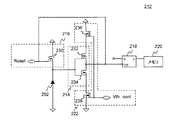
- 光を光電変換して電荷を生成する光電変換部と、
前記光電変換部で生成された電荷量が閾値以上となると第1信号を出力する検出部と、
前記光電変換部で生成された電荷量が前記閾値以上となった回数を計数する計数部と、
前記光電変換部に入射する光の強度が小さくなると周期が短くなり、光の強度が大きくなると周期が長くなる第2信号が、入力される入力部と、
前記第1信号と前記第2信号とに基づいて、前記光電変換部で生成された電荷の蓄積をリセットするリセット部と、
を備える撮像素子。 - 請求項1に記載の撮像素子において、
前記リセット部は、前記入力部に前記第2信号が入力されている間に、前記検出部から前記第1信号が出力されると、前記光電変換部で生成された電荷の蓄積をリセットする撮像素子。 - 請求項1または2に記載の撮像素子において、
前記入力部は、前記第1信号と前記第2信号とが入力され、
前記入力部は、前記第2信号が入力されている間に、前記第1信号が入力されると、前記光電変換部で生成された電荷の蓄積をリセットするよう前記リセット部に信号を出力する撮像素子。 - 請求項1から3のいずれか一項に記載の撮像素子において、
複数の前記光電変換部毎に前記閾値を制御する制御部と、
を備える撮像素子。 - 請求項4に記載の撮像素子において、
前記制御部は、前記光電変換部に入射する光の強度に基づいて前記閾値を制御する撮像素子。 - 請求項4または5に記載の撮像素子において、
前記制御部は、複数の前記光電変換部に入射する光の強度に基づいて、複数の前記光電変換部毎に前記閾値を制御する撮像素子。 - 請求項4から6のいずれか一項に記載の撮像素子において、
複数の前記制御部を備え、
複数の前記制御部はそれぞれ複数の前記光電変換部毎に1つ設けられ、複数の前記光電変換部毎に前記閾値を制御する撮像素子。 - 請求項1から7のいずれか一項に記載の撮像素子において、
前記検出部は、前記光電変換部で生成された電荷に基づく信号に基づいて、前記光電変換部で生成された電荷量が閾値以上となることを検出する撮像素子。 - 請求項1から8のいずれか一項に記載の撮像素子において、
前記計数部は、所定の期間内に、前記光電変換部で生成された電荷量が閾値以上になった回数を計数する撮像素子。 - 請求項1から9のいずれか一項に記載の撮像素子において、
前記計数部は、前記第1信号に基づいて、前記光電変換部で生成された電荷量が閾値以上になった回数を計数する撮像素子。 - 請求項1から10のいずれか一項に記載の撮像素子において、
前記計数部は、前記リセット部によりリセットされた回数を計数する撮像素子。 - 請求項1から11のいずれか一項に記載の撮像素子において、
前記光電変換部で生成された電荷に基づく信号が出力される出力部と、
前記第1信号を遅延させた信号を出力する遅延部を備え、
前記検出部は、前記遅延部から信号が出力されたタイミングにおいて前記出力部から出力される信号と、前記光電変換部で生成された電荷に基づく信号との差分が入力される撮像素子。 - 請求項1から12のいずれか一項に記載の撮像素子において、
複数の前記光電変換部が設けられる撮像チップと、
前記撮像チップに積層され、前記計数部が設けられる信号処理チップと、
を備える撮像素子。 - 請求項13に記載の撮像素子において、
前記検出部は、前記撮像チップに設けられる撮像素子。 - 請求項1から14のいずれか一項に記載の撮像素子を備える撮像装置。
Priority Applications (1)
| Application Number | Priority Date | Filing Date | Title |
|---|---|---|---|
| JP2017213249A JP6705436B2 (ja) | 2017-11-02 | 2017-11-02 | 撮像素子および撮像装置 |
Applications Claiming Priority (1)
| Application Number | Priority Date | Filing Date | Title |
|---|---|---|---|
| JP2017213249A JP6705436B2 (ja) | 2017-11-02 | 2017-11-02 | 撮像素子および撮像装置 |
Related Parent Applications (1)
| Application Number | Title | Priority Date | Filing Date |
|---|---|---|---|
| JP2013197318A Division JP6237045B2 (ja) | 2013-09-24 | 2013-09-24 | 撮像素子および撮像装置 |
Related Child Applications (1)
| Application Number | Title | Priority Date | Filing Date |
|---|---|---|---|
| JP2020085549A Division JP2020127243A (ja) | 2020-05-14 | 2020-05-14 | 撮像素子および撮像装置 |
Publications (3)
| Publication Number | Publication Date |
|---|---|
| JP2018050319A JP2018050319A (ja) | 2018-03-29 |
| JP2018050319A5 JP2018050319A5 (ja) | 2019-02-28 |
| JP6705436B2 true JP6705436B2 (ja) | 2020-06-03 |
Family
ID=61767844
Family Applications (1)
| Application Number | Title | Priority Date | Filing Date |
|---|---|---|---|
| JP2017213249A Active JP6705436B2 (ja) | 2017-11-02 | 2017-11-02 | 撮像素子および撮像装置 |
Country Status (1)
| Country | Link |
|---|---|
| JP (1) | JP6705436B2 (ja) |
Cited By (1)
| Publication number | Priority date | Publication date | Assignee | Title |
|---|---|---|---|---|
| JP2020127243A (ja) * | 2020-05-14 | 2020-08-20 | 株式会社ニコン | 撮像素子および撮像装置 |
Families Citing this family (2)
| Publication number | Priority date | Publication date | Assignee | Title |
|---|---|---|---|---|
| JP7468519B2 (ja) * | 2019-05-24 | 2024-04-16 | 株式会社ニコン | 撮像素子及び撮像装置 |
| JPWO2021162017A1 (ja) | 2020-02-14 | 2021-08-19 |
Family Cites Families (5)
| Publication number | Priority date | Publication date | Assignee | Title |
|---|---|---|---|---|
| JP3029363B2 (ja) * | 1993-08-23 | 2000-04-04 | 株式会社東芝 | 固体撮像装置 |
| JP3903361B2 (ja) * | 1999-08-13 | 2007-04-11 | 日本放送協会 | 固体撮像装置 |
| KR100834763B1 (ko) * | 2006-11-14 | 2008-06-05 | 삼성전자주식회사 | 동적 촬영 대역의 확장을 위한 이미지 센서 및 화소에수광된 광량을 측정하는 방법 |
| JP5269456B2 (ja) * | 2008-03-26 | 2013-08-21 | 株式会社東芝 | イメージセンサおよびその駆動方法 |
| JP5521721B2 (ja) * | 2009-08-28 | 2014-06-18 | ソニー株式会社 | 撮像素子およびカメラシステム |
-
2017
- 2017-11-02 JP JP2017213249A patent/JP6705436B2/ja active Active
Cited By (1)
| Publication number | Priority date | Publication date | Assignee | Title |
|---|---|---|---|---|
| JP2020127243A (ja) * | 2020-05-14 | 2020-08-20 | 株式会社ニコン | 撮像素子および撮像装置 |
Also Published As
| Publication number | Publication date |
|---|---|
| JP2018050319A (ja) | 2018-03-29 |
Similar Documents
| Publication | Publication Date | Title |
|---|---|---|
| JP6237045B2 (ja) | 撮像素子および撮像装置 | |
| JP6780745B2 (ja) | 電子機器 | |
| JP2023089131A (ja) | 撮像素子、および撮像装置 | |
| JP7222377B2 (ja) | 撮像素子および撮像装置 | |
| JP7473041B2 (ja) | 撮像素子、及び撮像装置 | |
| JP6354246B2 (ja) | 撮像装置、撮像装置の制御方法、及び制御プログラム | |
| JP6705436B2 (ja) | 撮像素子および撮像装置 | |
| JP2014179911A (ja) | 撮像装置 | |
| JP2015033036A (ja) | 撮像装置、撮像装置の制御方法、及び制御プログラム | |
| CN105934944B (zh) | 摄像元件及摄像装置 | |
| JP2014179778A (ja) | 信号処理装置、撮像素子、撮像装置および電子機器 | |
| JP6056572B2 (ja) | 撮像装置 | |
| JP2020127243A (ja) | 撮像素子および撮像装置 | |
| JP2014230242A (ja) | 撮像素子および撮像装置 | |
| JP6610648B2 (ja) | 撮像装置 | |
| US20230156367A1 (en) | Imaging element and imaging device | |
| JP6954391B2 (ja) | 電子機器 | |
| JP6597769B2 (ja) | 撮像素子および撮像装置 | |
| JP2023010785A (ja) | 撮像素子および撮像装置 | |
| JP2019083550A (ja) | 電子機器 | |
| JP6268782B2 (ja) | 撮像素子および撮像装置 | |
| JP2020205527A (ja) | 撮像装置、コンピュータプログラム及び記憶媒体 | |
| JP2017208397A (ja) | 裏面照射型固体撮像素子及び撮影装置 | |
| JP2017225172A (ja) | 撮像装置 | |
| JP2015023380A (ja) | 撮像素子および撮像装置 |
Legal Events
| Date | Code | Title | Description |
|---|---|---|---|
| A621 | Written request for application examination |
Free format text: JAPANESE INTERMEDIATE CODE: A621 Effective date: 20171201 |
|
| A521 | Request for written amendment filed |
Free format text: JAPANESE INTERMEDIATE CODE: A523 Effective date: 20190110 |
|
| A131 | Notification of reasons for refusal |
Free format text: JAPANESE INTERMEDIATE CODE: A131 Effective date: 20190212 |
|
| A601 | Written request for extension of time |
Free format text: JAPANESE INTERMEDIATE CODE: A601 Effective date: 20190412 |
|
| A521 | Request for written amendment filed |
Free format text: JAPANESE INTERMEDIATE CODE: A523 Effective date: 20190613 |
|
| A131 | Notification of reasons for refusal |
Free format text: JAPANESE INTERMEDIATE CODE: A131 Effective date: 20191112 |
|
| A521 | Request for written amendment filed |
Free format text: JAPANESE INTERMEDIATE CODE: A523 Effective date: 20191224 |
|
| TRDD | Decision of grant or rejection written | ||
| A01 | Written decision to grant a patent or to grant a registration (utility model) |
Free format text: JAPANESE INTERMEDIATE CODE: A01 Effective date: 20200414 |
|
| A61 | First payment of annual fees (during grant procedure) |
Free format text: JAPANESE INTERMEDIATE CODE: A61 Effective date: 20200427 |
|
| R150 | Certificate of patent or registration of utility model |
Ref document number: 6705436 Country of ref document: JP Free format text: JAPANESE INTERMEDIATE CODE: R150 |
|
| R250 | Receipt of annual fees |
Free format text: JAPANESE INTERMEDIATE CODE: R250 |