JP6685884B2 - Semiconductor module - Google Patents
Semiconductor module Download PDFInfo
- Publication number
- JP6685884B2 JP6685884B2 JP2016231244A JP2016231244A JP6685884B2 JP 6685884 B2 JP6685884 B2 JP 6685884B2 JP 2016231244 A JP2016231244 A JP 2016231244A JP 2016231244 A JP2016231244 A JP 2016231244A JP 6685884 B2 JP6685884 B2 JP 6685884B2
- Authority
- JP
- Japan
- Prior art keywords
- semiconductor package
- semiconductor
- wiring
- side conductor
- igbt
- Prior art date
- Legal status (The legal status is an assumption and is not a legal conclusion. Google has not performed a legal analysis and makes no representation as to the accuracy of the status listed.)
- Active
Links
Images


Classifications
-
- H—ELECTRICITY
- H01—ELECTRIC ELEMENTS
- H01L—SEMICONDUCTOR DEVICES NOT COVERED BY CLASS H10
- H01L23/00—Details of semiconductor or other solid state devices
- H01L23/34—Arrangements for cooling, heating, ventilating or temperature compensation ; Temperature sensing arrangements
- H01L23/36—Selection of materials, or shaping, to facilitate cooling or heating, e.g. heatsinks
- H01L23/373—Cooling facilitated by selection of materials for the device or materials for thermal expansion adaptation, e.g. carbon
-
- H—ELECTRICITY
- H01—ELECTRIC ELEMENTS
- H01L—SEMICONDUCTOR DEVICES NOT COVERED BY CLASS H10
- H01L23/00—Details of semiconductor or other solid state devices
- H01L23/34—Arrangements for cooling, heating, ventilating or temperature compensation ; Temperature sensing arrangements
- H01L23/42—Fillings or auxiliary members in containers or encapsulations selected or arranged to facilitate heating or cooling
- H01L23/433—Auxiliary members in containers characterised by their shape, e.g. pistons
- H01L23/4334—Auxiliary members in encapsulations
-
- H—ELECTRICITY
- H01—ELECTRIC ELEMENTS
- H01L—SEMICONDUCTOR DEVICES NOT COVERED BY CLASS H10
- H01L23/00—Details of semiconductor or other solid state devices
- H01L23/48—Arrangements for conducting electric current to or from the solid state body in operation, e.g. leads, terminal arrangements ; Selection of materials therefor
- H01L23/488—Arrangements for conducting electric current to or from the solid state body in operation, e.g. leads, terminal arrangements ; Selection of materials therefor consisting of soldered or bonded constructions
- H01L23/495—Lead-frames or other flat leads
- H01L23/49541—Geometry of the lead-frame
-
- H—ELECTRICITY
- H01—ELECTRIC ELEMENTS
- H01L—SEMICONDUCTOR DEVICES NOT COVERED BY CLASS H10
- H01L23/00—Details of semiconductor or other solid state devices
- H01L23/48—Arrangements for conducting electric current to or from the solid state body in operation, e.g. leads, terminal arrangements ; Selection of materials therefor
- H01L23/488—Arrangements for conducting electric current to or from the solid state body in operation, e.g. leads, terminal arrangements ; Selection of materials therefor consisting of soldered or bonded constructions
- H01L23/495—Lead-frames or other flat leads
- H01L23/49568—Lead-frames or other flat leads specifically adapted to facilitate heat dissipation
-
- H—ELECTRICITY
- H01—ELECTRIC ELEMENTS
- H01L—SEMICONDUCTOR DEVICES NOT COVERED BY CLASS H10
- H01L23/00—Details of semiconductor or other solid state devices
- H01L23/48—Arrangements for conducting electric current to or from the solid state body in operation, e.g. leads, terminal arrangements ; Selection of materials therefor
- H01L23/488—Arrangements for conducting electric current to or from the solid state body in operation, e.g. leads, terminal arrangements ; Selection of materials therefor consisting of soldered or bonded constructions
- H01L23/498—Leads, i.e. metallisations or lead-frames on insulating substrates, e.g. chip carriers
- H01L23/49811—Additional leads joined to the metallisation on the insulating substrate, e.g. pins, bumps, wires, flat leads
-
- H—ELECTRICITY
- H01—ELECTRIC ELEMENTS
- H01L—SEMICONDUCTOR DEVICES NOT COVERED BY CLASS H10
- H01L23/00—Details of semiconductor or other solid state devices
- H01L23/48—Arrangements for conducting electric current to or from the solid state body in operation, e.g. leads, terminal arrangements ; Selection of materials therefor
- H01L23/488—Arrangements for conducting electric current to or from the solid state body in operation, e.g. leads, terminal arrangements ; Selection of materials therefor consisting of soldered or bonded constructions
- H01L23/498—Leads, i.e. metallisations or lead-frames on insulating substrates, e.g. chip carriers
- H01L23/49838—Geometry or layout
- H01L23/49844—Geometry or layout for devices being provided for in H01L29/00
-
- H—ELECTRICITY
- H01—ELECTRIC ELEMENTS
- H01L—SEMICONDUCTOR DEVICES NOT COVERED BY CLASS H10
- H01L23/00—Details of semiconductor or other solid state devices
- H01L23/52—Arrangements for conducting electric current within the device in operation from one component to another, i.e. interconnections, e.g. wires, lead frames
- H01L23/522—Arrangements for conducting electric current within the device in operation from one component to another, i.e. interconnections, e.g. wires, lead frames including external interconnections consisting of a multilayer structure of conductive and insulating layers inseparably formed on the semiconductor body
- H01L23/5226—Via connections in a multilevel interconnection structure
-
- H—ELECTRICITY
- H01—ELECTRIC ELEMENTS
- H01L—SEMICONDUCTOR DEVICES NOT COVERED BY CLASS H10
- H01L23/00—Details of semiconductor or other solid state devices
- H01L23/52—Arrangements for conducting electric current within the device in operation from one component to another, i.e. interconnections, e.g. wires, lead frames
- H01L23/522—Arrangements for conducting electric current within the device in operation from one component to another, i.e. interconnections, e.g. wires, lead frames including external interconnections consisting of a multilayer structure of conductive and insulating layers inseparably formed on the semiconductor body
- H01L23/532—Arrangements for conducting electric current within the device in operation from one component to another, i.e. interconnections, e.g. wires, lead frames including external interconnections consisting of a multilayer structure of conductive and insulating layers inseparably formed on the semiconductor body characterised by the materials
- H01L23/53204—Conductive materials
- H01L23/53209—Conductive materials based on metals, e.g. alloys, metal silicides
- H01L23/53228—Conductive materials based on metals, e.g. alloys, metal silicides the principal metal being copper
-
- H—ELECTRICITY
- H01—ELECTRIC ELEMENTS
- H01L—SEMICONDUCTOR DEVICES NOT COVERED BY CLASS H10
- H01L23/00—Details of semiconductor or other solid state devices
- H01L23/52—Arrangements for conducting electric current within the device in operation from one component to another, i.e. interconnections, e.g. wires, lead frames
- H01L23/538—Arrangements for conducting electric current within the device in operation from one component to another, i.e. interconnections, e.g. wires, lead frames the interconnection structure between a plurality of semiconductor chips being formed on, or in, insulating substrates
- H01L23/5386—Geometry or layout of the interconnection structure
-
- H—ELECTRICITY
- H01—ELECTRIC ELEMENTS
- H01L—SEMICONDUCTOR DEVICES NOT COVERED BY CLASS H10
- H01L24/00—Arrangements for connecting or disconnecting semiconductor or solid-state bodies; Methods or apparatus related thereto
-
- H—ELECTRICITY
- H01—ELECTRIC ELEMENTS
- H01L—SEMICONDUCTOR DEVICES NOT COVERED BY CLASS H10
- H01L24/00—Arrangements for connecting or disconnecting semiconductor or solid-state bodies; Methods or apparatus related thereto
- H01L24/01—Means for bonding being attached to, or being formed on, the surface to be connected, e.g. chip-to-package, die-attach, "first-level" interconnects; Manufacturing methods related thereto
- H01L24/34—Strap connectors, e.g. copper straps for grounding power devices; Manufacturing methods related thereto
- H01L24/39—Structure, shape, material or disposition of the strap connectors after the connecting process
- H01L24/40—Structure, shape, material or disposition of the strap connectors after the connecting process of an individual strap connector
-
- H—ELECTRICITY
- H01—ELECTRIC ELEMENTS
- H01L—SEMICONDUCTOR DEVICES NOT COVERED BY CLASS H10
- H01L25/00—Assemblies consisting of a plurality of individual semiconductor or other solid state devices ; Multistep manufacturing processes thereof
- H01L25/03—Assemblies consisting of a plurality of individual semiconductor or other solid state devices ; Multistep manufacturing processes thereof all the devices being of a type provided for in the same subgroup of groups H01L27/00 - H01L33/00, or in a single subclass of H10K, H10N, e.g. assemblies of rectifier diodes
- H01L25/04—Assemblies consisting of a plurality of individual semiconductor or other solid state devices ; Multistep manufacturing processes thereof all the devices being of a type provided for in the same subgroup of groups H01L27/00 - H01L33/00, or in a single subclass of H10K, H10N, e.g. assemblies of rectifier diodes the devices not having separate containers
- H01L25/07—Assemblies consisting of a plurality of individual semiconductor or other solid state devices ; Multistep manufacturing processes thereof all the devices being of a type provided for in the same subgroup of groups H01L27/00 - H01L33/00, or in a single subclass of H10K, H10N, e.g. assemblies of rectifier diodes the devices not having separate containers the devices being of a type provided for in group H01L29/00
- H01L25/074—Stacked arrangements of non-apertured devices
-
- H—ELECTRICITY
- H01—ELECTRIC ELEMENTS
- H01L—SEMICONDUCTOR DEVICES NOT COVERED BY CLASS H10
- H01L25/00—Assemblies consisting of a plurality of individual semiconductor or other solid state devices ; Multistep manufacturing processes thereof
- H01L25/03—Assemblies consisting of a plurality of individual semiconductor or other solid state devices ; Multistep manufacturing processes thereof all the devices being of a type provided for in the same subgroup of groups H01L27/00 - H01L33/00, or in a single subclass of H10K, H10N, e.g. assemblies of rectifier diodes
- H01L25/10—Assemblies consisting of a plurality of individual semiconductor or other solid state devices ; Multistep manufacturing processes thereof all the devices being of a type provided for in the same subgroup of groups H01L27/00 - H01L33/00, or in a single subclass of H10K, H10N, e.g. assemblies of rectifier diodes the devices having separate containers
- H01L25/11—Assemblies consisting of a plurality of individual semiconductor or other solid state devices ; Multistep manufacturing processes thereof all the devices being of a type provided for in the same subgroup of groups H01L27/00 - H01L33/00, or in a single subclass of H10K, H10N, e.g. assemblies of rectifier diodes the devices having separate containers the devices being of a type provided for in group H01L29/00
- H01L25/115—Assemblies consisting of a plurality of individual semiconductor or other solid state devices ; Multistep manufacturing processes thereof all the devices being of a type provided for in the same subgroup of groups H01L27/00 - H01L33/00, or in a single subclass of H10K, H10N, e.g. assemblies of rectifier diodes the devices having separate containers the devices being of a type provided for in group H01L29/00 the devices being arranged next to each other
-
- H—ELECTRICITY
- H01—ELECTRIC ELEMENTS
- H01L—SEMICONDUCTOR DEVICES NOT COVERED BY CLASS H10
- H01L2224/00—Indexing scheme for arrangements for connecting or disconnecting semiconductor or solid-state bodies and methods related thereto as covered by H01L24/00
- H01L2224/01—Means for bonding being attached to, or being formed on, the surface to be connected, e.g. chip-to-package, die-attach, "first-level" interconnects; Manufacturing methods related thereto
- H01L2224/26—Layer connectors, e.g. plate connectors, solder or adhesive layers; Manufacturing methods related thereto
- H01L2224/2612—Auxiliary members for layer connectors, e.g. spacers
-
- H—ELECTRICITY
- H01—ELECTRIC ELEMENTS
- H01L—SEMICONDUCTOR DEVICES NOT COVERED BY CLASS H10
- H01L2224/00—Indexing scheme for arrangements for connecting or disconnecting semiconductor or solid-state bodies and methods related thereto as covered by H01L24/00
- H01L2224/01—Means for bonding being attached to, or being formed on, the surface to be connected, e.g. chip-to-package, die-attach, "first-level" interconnects; Manufacturing methods related thereto
- H01L2224/26—Layer connectors, e.g. plate connectors, solder or adhesive layers; Manufacturing methods related thereto
- H01L2224/28—Structure, shape, material or disposition of the layer connectors prior to the connecting process
- H01L2224/29—Structure, shape, material or disposition of the layer connectors prior to the connecting process of an individual layer connector
- H01L2224/29001—Core members of the layer connector
- H01L2224/29099—Material
- H01L2224/291—Material with a principal constituent of the material being a metal or a metalloid, e.g. boron [B], silicon [Si], germanium [Ge], arsenic [As], antimony [Sb], tellurium [Te] and polonium [Po], and alloys thereof
- H01L2224/29101—Material with a principal constituent of the material being a metal or a metalloid, e.g. boron [B], silicon [Si], germanium [Ge], arsenic [As], antimony [Sb], tellurium [Te] and polonium [Po], and alloys thereof the principal constituent melting at a temperature of less than 400°C
-
- H—ELECTRICITY
- H01—ELECTRIC ELEMENTS
- H01L—SEMICONDUCTOR DEVICES NOT COVERED BY CLASS H10
- H01L2224/00—Indexing scheme for arrangements for connecting or disconnecting semiconductor or solid-state bodies and methods related thereto as covered by H01L24/00
- H01L2224/01—Means for bonding being attached to, or being formed on, the surface to be connected, e.g. chip-to-package, die-attach, "first-level" interconnects; Manufacturing methods related thereto
- H01L2224/26—Layer connectors, e.g. plate connectors, solder or adhesive layers; Manufacturing methods related thereto
- H01L2224/28—Structure, shape, material or disposition of the layer connectors prior to the connecting process
- H01L2224/29—Structure, shape, material or disposition of the layer connectors prior to the connecting process of an individual layer connector
- H01L2224/29001—Core members of the layer connector
- H01L2224/29099—Material
- H01L2224/29198—Material with a principal constituent of the material being a combination of two or more materials in the form of a matrix with a filler, i.e. being a hybrid material, e.g. segmented structures, foams
- H01L2224/29298—Fillers
- H01L2224/29299—Base material
- H01L2224/293—Base material with a principal constituent of the material being a metal or a metalloid, e.g. boron [B], silicon [Si], germanium [Ge], arsenic [As], antimony [Sb], tellurium [Te] and polonium [Po], and alloys thereof
- H01L2224/29338—Base material with a principal constituent of the material being a metal or a metalloid, e.g. boron [B], silicon [Si], germanium [Ge], arsenic [As], antimony [Sb], tellurium [Te] and polonium [Po], and alloys thereof the principal constituent melting at a temperature of greater than or equal to 950°C and less than 1550°C
- H01L2224/29339—Silver [Ag] as principal constituent
-
- H—ELECTRICITY
- H01—ELECTRIC ELEMENTS
- H01L—SEMICONDUCTOR DEVICES NOT COVERED BY CLASS H10
- H01L2224/00—Indexing scheme for arrangements for connecting or disconnecting semiconductor or solid-state bodies and methods related thereto as covered by H01L24/00
- H01L2224/01—Means for bonding being attached to, or being formed on, the surface to be connected, e.g. chip-to-package, die-attach, "first-level" interconnects; Manufacturing methods related thereto
- H01L2224/26—Layer connectors, e.g. plate connectors, solder or adhesive layers; Manufacturing methods related thereto
- H01L2224/31—Structure, shape, material or disposition of the layer connectors after the connecting process
- H01L2224/33—Structure, shape, material or disposition of the layer connectors after the connecting process of a plurality of layer connectors
- H01L2224/331—Disposition
- H01L2224/3318—Disposition being disposed on at least two different sides of the body, e.g. dual array
- H01L2224/33181—On opposite sides of the body
-
- H—ELECTRICITY
- H01—ELECTRIC ELEMENTS
- H01L—SEMICONDUCTOR DEVICES NOT COVERED BY CLASS H10
- H01L2224/00—Indexing scheme for arrangements for connecting or disconnecting semiconductor or solid-state bodies and methods related thereto as covered by H01L24/00
- H01L2224/01—Means for bonding being attached to, or being formed on, the surface to be connected, e.g. chip-to-package, die-attach, "first-level" interconnects; Manufacturing methods related thereto
- H01L2224/34—Strap connectors, e.g. copper straps for grounding power devices; Manufacturing methods related thereto
- H01L2224/36—Structure, shape, material or disposition of the strap connectors prior to the connecting process
- H01L2224/37—Structure, shape, material or disposition of the strap connectors prior to the connecting process of an individual strap connector
- H01L2224/3754—Coating
- H01L2224/37599—Material
-
- H—ELECTRICITY
- H01—ELECTRIC ELEMENTS
- H01L—SEMICONDUCTOR DEVICES NOT COVERED BY CLASS H10
- H01L2224/00—Indexing scheme for arrangements for connecting or disconnecting semiconductor or solid-state bodies and methods related thereto as covered by H01L24/00
- H01L2224/01—Means for bonding being attached to, or being formed on, the surface to be connected, e.g. chip-to-package, die-attach, "first-level" interconnects; Manufacturing methods related thereto
- H01L2224/34—Strap connectors, e.g. copper straps for grounding power devices; Manufacturing methods related thereto
- H01L2224/39—Structure, shape, material or disposition of the strap connectors after the connecting process
- H01L2224/40—Structure, shape, material or disposition of the strap connectors after the connecting process of an individual strap connector
- H01L2224/401—Disposition
- H01L2224/40135—Connecting between different semiconductor or solid-state bodies, i.e. chip-to-chip
- H01L2224/40137—Connecting between different semiconductor or solid-state bodies, i.e. chip-to-chip the bodies being arranged next to each other, e.g. on a common substrate
- H01L2224/40139—Connecting between different semiconductor or solid-state bodies, i.e. chip-to-chip the bodies being arranged next to each other, e.g. on a common substrate with an intermediate bond, e.g. continuous strap daisy chain
-
- H—ELECTRICITY
- H01—ELECTRIC ELEMENTS
- H01L—SEMICONDUCTOR DEVICES NOT COVERED BY CLASS H10
- H01L2224/00—Indexing scheme for arrangements for connecting or disconnecting semiconductor or solid-state bodies and methods related thereto as covered by H01L24/00
- H01L2224/01—Means for bonding being attached to, or being formed on, the surface to be connected, e.g. chip-to-package, die-attach, "first-level" interconnects; Manufacturing methods related thereto
- H01L2224/42—Wire connectors; Manufacturing methods related thereto
- H01L2224/47—Structure, shape, material or disposition of the wire connectors after the connecting process
- H01L2224/48—Structure, shape, material or disposition of the wire connectors after the connecting process of an individual wire connector
- H01L2224/4805—Shape
- H01L2224/4809—Loop shape
- H01L2224/48091—Arched
-
- H—ELECTRICITY
- H01—ELECTRIC ELEMENTS
- H01L—SEMICONDUCTOR DEVICES NOT COVERED BY CLASS H10
- H01L2224/00—Indexing scheme for arrangements for connecting or disconnecting semiconductor or solid-state bodies and methods related thereto as covered by H01L24/00
- H01L2224/01—Means for bonding being attached to, or being formed on, the surface to be connected, e.g. chip-to-package, die-attach, "first-level" interconnects; Manufacturing methods related thereto
- H01L2224/42—Wire connectors; Manufacturing methods related thereto
- H01L2224/47—Structure, shape, material or disposition of the wire connectors after the connecting process
- H01L2224/48—Structure, shape, material or disposition of the wire connectors after the connecting process of an individual wire connector
- H01L2224/481—Disposition
- H01L2224/48151—Connecting between a semiconductor or solid-state body and an item not being a semiconductor or solid-state body, e.g. chip-to-substrate, chip-to-passive
- H01L2224/48221—Connecting between a semiconductor or solid-state body and an item not being a semiconductor or solid-state body, e.g. chip-to-substrate, chip-to-passive the body and the item being stacked
- H01L2224/48245—Connecting between a semiconductor or solid-state body and an item not being a semiconductor or solid-state body, e.g. chip-to-substrate, chip-to-passive the body and the item being stacked the item being metallic
- H01L2224/48247—Connecting between a semiconductor or solid-state body and an item not being a semiconductor or solid-state body, e.g. chip-to-substrate, chip-to-passive the body and the item being stacked the item being metallic connecting the wire to a bond pad of the item
-
- H—ELECTRICITY
- H01—ELECTRIC ELEMENTS
- H01L—SEMICONDUCTOR DEVICES NOT COVERED BY CLASS H10
- H01L2224/00—Indexing scheme for arrangements for connecting or disconnecting semiconductor or solid-state bodies and methods related thereto as covered by H01L24/00
- H01L2224/73—Means for bonding being of different types provided for in two or more of groups H01L2224/10, H01L2224/18, H01L2224/26, H01L2224/34, H01L2224/42, H01L2224/50, H01L2224/63, H01L2224/71
- H01L2224/732—Location after the connecting process
- H01L2224/73201—Location after the connecting process on the same surface
- H01L2224/73215—Layer and wire connectors
-
- H—ELECTRICITY
- H01—ELECTRIC ELEMENTS
- H01L—SEMICONDUCTOR DEVICES NOT COVERED BY CLASS H10
- H01L2224/00—Indexing scheme for arrangements for connecting or disconnecting semiconductor or solid-state bodies and methods related thereto as covered by H01L24/00
- H01L2224/73—Means for bonding being of different types provided for in two or more of groups H01L2224/10, H01L2224/18, H01L2224/26, H01L2224/34, H01L2224/42, H01L2224/50, H01L2224/63, H01L2224/71
- H01L2224/732—Location after the connecting process
- H01L2224/73201—Location after the connecting process on the same surface
- H01L2224/73221—Strap and wire connectors
-
- H—ELECTRICITY
- H01—ELECTRIC ELEMENTS
- H01L—SEMICONDUCTOR DEVICES NOT COVERED BY CLASS H10
- H01L2224/00—Indexing scheme for arrangements for connecting or disconnecting semiconductor or solid-state bodies and methods related thereto as covered by H01L24/00
- H01L2224/73—Means for bonding being of different types provided for in two or more of groups H01L2224/10, H01L2224/18, H01L2224/26, H01L2224/34, H01L2224/42, H01L2224/50, H01L2224/63, H01L2224/71
- H01L2224/732—Location after the connecting process
- H01L2224/73251—Location after the connecting process on different surfaces
- H01L2224/73265—Layer and wire connectors
-
- H—ELECTRICITY
- H01—ELECTRIC ELEMENTS
- H01L—SEMICONDUCTOR DEVICES NOT COVERED BY CLASS H10
- H01L2224/00—Indexing scheme for arrangements for connecting or disconnecting semiconductor or solid-state bodies and methods related thereto as covered by H01L24/00
- H01L2224/80—Methods for connecting semiconductor or other solid state bodies using means for bonding being attached to, or being formed on, the surface to be connected
- H01L2224/83—Methods for connecting semiconductor or other solid state bodies using means for bonding being attached to, or being formed on, the surface to be connected using a layer connector
- H01L2224/838—Bonding techniques
- H01L2224/83801—Soldering or alloying
-
- H—ELECTRICITY
- H01—ELECTRIC ELEMENTS
- H01L—SEMICONDUCTOR DEVICES NOT COVERED BY CLASS H10
- H01L2224/00—Indexing scheme for arrangements for connecting or disconnecting semiconductor or solid-state bodies and methods related thereto as covered by H01L24/00
- H01L2224/80—Methods for connecting semiconductor or other solid state bodies using means for bonding being attached to, or being formed on, the surface to be connected
- H01L2224/84—Methods for connecting semiconductor or other solid state bodies using means for bonding being attached to, or being formed on, the surface to be connected using a strap connector
- H01L2224/848—Bonding techniques
- H01L2224/84801—Soldering or alloying
-
- H—ELECTRICITY
- H01—ELECTRIC ELEMENTS
- H01L—SEMICONDUCTOR DEVICES NOT COVERED BY CLASS H10
- H01L23/00—Details of semiconductor or other solid state devices
- H01L23/34—Arrangements for cooling, heating, ventilating or temperature compensation ; Temperature sensing arrangements
- H01L23/36—Selection of materials, or shaping, to facilitate cooling or heating, e.g. heatsinks
- H01L23/373—Cooling facilitated by selection of materials for the device or materials for thermal expansion adaptation, e.g. carbon
- H01L23/3735—Laminates or multilayers, e.g. direct bond copper ceramic substrates
-
- H—ELECTRICITY
- H01—ELECTRIC ELEMENTS
- H01L—SEMICONDUCTOR DEVICES NOT COVERED BY CLASS H10
- H01L23/00—Details of semiconductor or other solid state devices
- H01L23/48—Arrangements for conducting electric current to or from the solid state body in operation, e.g. leads, terminal arrangements ; Selection of materials therefor
- H01L23/488—Arrangements for conducting electric current to or from the solid state body in operation, e.g. leads, terminal arrangements ; Selection of materials therefor consisting of soldered or bonded constructions
- H01L23/495—Lead-frames or other flat leads
- H01L23/49541—Geometry of the lead-frame
- H01L23/49548—Cross section geometry
-
- H—ELECTRICITY
- H01—ELECTRIC ELEMENTS
- H01L—SEMICONDUCTOR DEVICES NOT COVERED BY CLASS H10
- H01L23/00—Details of semiconductor or other solid state devices
- H01L23/48—Arrangements for conducting electric current to or from the solid state body in operation, e.g. leads, terminal arrangements ; Selection of materials therefor
- H01L23/488—Arrangements for conducting electric current to or from the solid state body in operation, e.g. leads, terminal arrangements ; Selection of materials therefor consisting of soldered or bonded constructions
- H01L23/495—Lead-frames or other flat leads
- H01L23/49541—Geometry of the lead-frame
- H01L23/49562—Geometry of the lead-frame for devices being provided for in H01L29/00
-
- H—ELECTRICITY
- H01—ELECTRIC ELEMENTS
- H01L—SEMICONDUCTOR DEVICES NOT COVERED BY CLASS H10
- H01L23/00—Details of semiconductor or other solid state devices
- H01L23/48—Arrangements for conducting electric current to or from the solid state body in operation, e.g. leads, terminal arrangements ; Selection of materials therefor
- H01L23/488—Arrangements for conducting electric current to or from the solid state body in operation, e.g. leads, terminal arrangements ; Selection of materials therefor consisting of soldered or bonded constructions
- H01L23/498—Leads, i.e. metallisations or lead-frames on insulating substrates, e.g. chip carriers
- H01L23/49861—Lead-frames fixed on or encapsulated in insulating substrates
-
- H—ELECTRICITY
- H01—ELECTRIC ELEMENTS
- H01L—SEMICONDUCTOR DEVICES NOT COVERED BY CLASS H10
- H01L24/00—Arrangements for connecting or disconnecting semiconductor or solid-state bodies; Methods or apparatus related thereto
- H01L24/01—Means for bonding being attached to, or being formed on, the surface to be connected, e.g. chip-to-package, die-attach, "first-level" interconnects; Manufacturing methods related thereto
- H01L24/26—Layer connectors, e.g. plate connectors, solder or adhesive layers; Manufacturing methods related thereto
- H01L24/28—Structure, shape, material or disposition of the layer connectors prior to the connecting process
- H01L24/29—Structure, shape, material or disposition of the layer connectors prior to the connecting process of an individual layer connector
-
- H—ELECTRICITY
- H01—ELECTRIC ELEMENTS
- H01L—SEMICONDUCTOR DEVICES NOT COVERED BY CLASS H10
- H01L24/00—Arrangements for connecting or disconnecting semiconductor or solid-state bodies; Methods or apparatus related thereto
- H01L24/01—Means for bonding being attached to, or being formed on, the surface to be connected, e.g. chip-to-package, die-attach, "first-level" interconnects; Manufacturing methods related thereto
- H01L24/26—Layer connectors, e.g. plate connectors, solder or adhesive layers; Manufacturing methods related thereto
- H01L24/31—Structure, shape, material or disposition of the layer connectors after the connecting process
- H01L24/32—Structure, shape, material or disposition of the layer connectors after the connecting process of an individual layer connector
-
- H—ELECTRICITY
- H01—ELECTRIC ELEMENTS
- H01L—SEMICONDUCTOR DEVICES NOT COVERED BY CLASS H10
- H01L24/00—Arrangements for connecting or disconnecting semiconductor or solid-state bodies; Methods or apparatus related thereto
- H01L24/01—Means for bonding being attached to, or being formed on, the surface to be connected, e.g. chip-to-package, die-attach, "first-level" interconnects; Manufacturing methods related thereto
- H01L24/26—Layer connectors, e.g. plate connectors, solder or adhesive layers; Manufacturing methods related thereto
- H01L24/31—Structure, shape, material or disposition of the layer connectors after the connecting process
- H01L24/33—Structure, shape, material or disposition of the layer connectors after the connecting process of a plurality of layer connectors
-
- H—ELECTRICITY
- H01—ELECTRIC ELEMENTS
- H01L—SEMICONDUCTOR DEVICES NOT COVERED BY CLASS H10
- H01L24/00—Arrangements for connecting or disconnecting semiconductor or solid-state bodies; Methods or apparatus related thereto
- H01L24/01—Means for bonding being attached to, or being formed on, the surface to be connected, e.g. chip-to-package, die-attach, "first-level" interconnects; Manufacturing methods related thereto
- H01L24/42—Wire connectors; Manufacturing methods related thereto
- H01L24/47—Structure, shape, material or disposition of the wire connectors after the connecting process
- H01L24/48—Structure, shape, material or disposition of the wire connectors after the connecting process of an individual wire connector
-
- H—ELECTRICITY
- H01—ELECTRIC ELEMENTS
- H01L—SEMICONDUCTOR DEVICES NOT COVERED BY CLASS H10
- H01L24/00—Arrangements for connecting or disconnecting semiconductor or solid-state bodies; Methods or apparatus related thereto
- H01L24/80—Methods for connecting semiconductor or other solid state bodies using means for bonding being attached to, or being formed on, the surface to be connected
- H01L24/83—Methods for connecting semiconductor or other solid state bodies using means for bonding being attached to, or being formed on, the surface to be connected using a layer connector
-
- H—ELECTRICITY
- H01—ELECTRIC ELEMENTS
- H01L—SEMICONDUCTOR DEVICES NOT COVERED BY CLASS H10
- H01L24/00—Arrangements for connecting or disconnecting semiconductor or solid-state bodies; Methods or apparatus related thereto
- H01L24/80—Methods for connecting semiconductor or other solid state bodies using means for bonding being attached to, or being formed on, the surface to be connected
- H01L24/84—Methods for connecting semiconductor or other solid state bodies using means for bonding being attached to, or being formed on, the surface to be connected using a strap connector
-
- H—ELECTRICITY
- H01—ELECTRIC ELEMENTS
- H01L—SEMICONDUCTOR DEVICES NOT COVERED BY CLASS H10
- H01L2924/00—Indexing scheme for arrangements or methods for connecting or disconnecting semiconductor or solid-state bodies as covered by H01L24/00
- H01L2924/0001—Technical content checked by a classifier
- H01L2924/00014—Technical content checked by a classifier the subject-matter covered by the group, the symbol of which is combined with the symbol of this group, being disclosed without further technical details
-
- H—ELECTRICITY
- H01—ELECTRIC ELEMENTS
- H01L—SEMICONDUCTOR DEVICES NOT COVERED BY CLASS H10
- H01L2924/00—Indexing scheme for arrangements or methods for connecting or disconnecting semiconductor or solid-state bodies as covered by H01L24/00
- H01L2924/10—Details of semiconductor or other solid state devices to be connected
- H01L2924/102—Material of the semiconductor or solid state bodies
- H01L2924/1025—Semiconducting materials
- H01L2924/10251—Elemental semiconductors, i.e. Group IV
- H01L2924/10253—Silicon [Si]
-
- H—ELECTRICITY
- H01—ELECTRIC ELEMENTS
- H01L—SEMICONDUCTOR DEVICES NOT COVERED BY CLASS H10
- H01L2924/00—Indexing scheme for arrangements or methods for connecting or disconnecting semiconductor or solid-state bodies as covered by H01L24/00
- H01L2924/10—Details of semiconductor or other solid state devices to be connected
- H01L2924/102—Material of the semiconductor or solid state bodies
- H01L2924/1025—Semiconducting materials
- H01L2924/1026—Compound semiconductors
- H01L2924/1027—IV
- H01L2924/10272—Silicon Carbide [SiC]
-
- H—ELECTRICITY
- H01—ELECTRIC ELEMENTS
- H01L—SEMICONDUCTOR DEVICES NOT COVERED BY CLASS H10
- H01L2924/00—Indexing scheme for arrangements or methods for connecting or disconnecting semiconductor or solid-state bodies as covered by H01L24/00
- H01L2924/10—Details of semiconductor or other solid state devices to be connected
- H01L2924/102—Material of the semiconductor or solid state bodies
- H01L2924/1025—Semiconducting materials
- H01L2924/1026—Compound semiconductors
- H01L2924/1032—III-V
- H01L2924/1033—Gallium nitride [GaN]
-
- H—ELECTRICITY
- H01—ELECTRIC ELEMENTS
- H01L—SEMICONDUCTOR DEVICES NOT COVERED BY CLASS H10
- H01L2924/00—Indexing scheme for arrangements or methods for connecting or disconnecting semiconductor or solid-state bodies as covered by H01L24/00
- H01L2924/10—Details of semiconductor or other solid state devices to be connected
- H01L2924/11—Device type
- H01L2924/12—Passive devices, e.g. 2 terminal devices
- H01L2924/1203—Rectifying Diode
-
- H—ELECTRICITY
- H01—ELECTRIC ELEMENTS
- H01L—SEMICONDUCTOR DEVICES NOT COVERED BY CLASS H10
- H01L2924/00—Indexing scheme for arrangements or methods for connecting or disconnecting semiconductor or solid-state bodies as covered by H01L24/00
- H01L2924/10—Details of semiconductor or other solid state devices to be connected
- H01L2924/11—Device type
- H01L2924/13—Discrete devices, e.g. 3 terminal devices
- H01L2924/1304—Transistor
- H01L2924/1305—Bipolar Junction Transistor [BJT]
- H01L2924/13055—Insulated gate bipolar transistor [IGBT]
-
- H—ELECTRICITY
- H01—ELECTRIC ELEMENTS
- H01L—SEMICONDUCTOR DEVICES NOT COVERED BY CLASS H10
- H01L2924/00—Indexing scheme for arrangements or methods for connecting or disconnecting semiconductor or solid-state bodies as covered by H01L24/00
- H01L2924/10—Details of semiconductor or other solid state devices to be connected
- H01L2924/11—Device type
- H01L2924/13—Discrete devices, e.g. 3 terminal devices
- H01L2924/1304—Transistor
- H01L2924/1306—Field-effect transistor [FET]
- H01L2924/13091—Metal-Oxide-Semiconductor Field-Effect Transistor [MOSFET]
-
- H—ELECTRICITY
- H01—ELECTRIC ELEMENTS
- H01L—SEMICONDUCTOR DEVICES NOT COVERED BY CLASS H10
- H01L2924/00—Indexing scheme for arrangements or methods for connecting or disconnecting semiconductor or solid-state bodies as covered by H01L24/00
- H01L2924/15—Details of package parts other than the semiconductor or other solid state devices to be connected
- H01L2924/181—Encapsulation
Landscapes
- Engineering & Computer Science (AREA)
- Microelectronics & Electronic Packaging (AREA)
- Power Engineering (AREA)
- Physics & Mathematics (AREA)
- Computer Hardware Design (AREA)
- Condensed Matter Physics & Semiconductors (AREA)
- General Physics & Mathematics (AREA)
- Geometry (AREA)
- Chemical & Material Sciences (AREA)
- Materials Engineering (AREA)
- Cooling Or The Like Of Semiconductors Or Solid State Devices (AREA)
Description
本発明による実施形態は、半導体モジュールに関する。 Embodiments according to the present invention relate to semiconductor modules.
従来の半導体パワーモジュールにおいては、例えば、表裏面に銅箔が貼り付けられたセ
ラミック板に半田を介して半導体チップが実装されており、半導体チップを実装したセラ
ミック板は、半田を介して金属ベース基板に実装されていた。このような半導体パワーモ
ジュールは、例えば、セラミック板の線膨張係数を半導体チップの線膨張係数に近付ける
ことで温度サイクル耐量およびパワーサイクル耐量を向上させている。
In a conventional semiconductor power module, for example, a semiconductor chip is mounted on a ceramic plate having copper foils attached to the front and back sides via solder, and the ceramic plate on which the semiconductor chip is mounted uses a metal base via solder. It was mounted on the board. In such a semiconductor power module, for example, the thermal cycle resistance and the power cycle resistance are improved by bringing the linear expansion coefficient of the ceramic plate close to the linear expansion coefficient of the semiconductor chip.
しかしながら、従来の半導体パワーモジュールでは、半導体チップで発生した熱の殆ど
を半導体チップの下面から金属ベース板へ放熱するのみであった。
However, in the conventional semiconductor power module, most of the heat generated in the semiconductor chip is only radiated from the lower surface of the semiconductor chip to the metal base plate.
本実施形態による半導体モジュールは、金属層と、前記金属層上に設けられ樹脂を含有する絶縁層と、を有する基板と、前記基板上に設けられた第1配線および第2配線と、前記第1配線上に設けられ、上部および下部において放熱する第1半導体パッケージと、前記第1半導体パッケージ上部及び前記第2配線に接続し、熱伝導性を有する第3配線と、を備える半導体モジュール。 The semiconductor module according to the present embodiment has a substrate having a metal layer and an insulating layer containing a resin provided on the metal layer, a first wiring and a second wiring provided on the substrate, and the first wiring. A semiconductor module comprising: a first semiconductor package which is provided on one wiring and radiates heat at an upper portion and a lower portion; and a third wiring which is connected to the first semiconductor package upper portion and the second wiring and has thermal conductivity.
実施形態に係る半導体モジュールは、金属層と、前記金属層上に設けられ樹脂を含有す A semiconductor module according to an embodiment includes a metal layer and a resin provided on the metal layer.
る絶縁層と、を有する基板と、前記基板上に設けられた第6配線と、前記第6配線上に設A substrate having an insulating layer, a sixth wiring provided on the substrate, and a wiring provided on the sixth wiring.
けられ、上部および下部において放熱する第1半導体パッケージと、前記第6配線上に、And the first semiconductor package that radiates heat in the upper and lower portions and the sixth wiring,
前記第1半導体パッケージに対して上下反転して設けられ、上部および下部において放熱It is provided upside down with respect to the first semiconductor package and radiates heat in the upper and lower parts
する第2半導体パッケージと、前記第1半導体パッケージ上に設けられた第4配線と、前A second semiconductor package, a fourth wiring provided on the first semiconductor package, and
記第2半導体パッケージ上に設けられた第5配線と、を備え、前記第1半導体パッケージA fifth wiring provided on the second semiconductor package, and the first semiconductor package
と前記第2半導体パッケージは前記第6配線を介して、直列接続される半導体モジュールA semiconductor module in which the second semiconductor package and the second semiconductor package are connected in series via the sixth wiring.
。.
以下、図面を参照して本発明に係る実施形態を説明する。以下の実施形態では、半導体
モジュールの特徴的な構成および動作を中心に説明するが、半導体モジュールには以下の
説明で省略した構成および動作が存在しうる。これらの省略した構成および動作も本実施
形態の範囲に含まれるものである。
Hereinafter, embodiments according to the present invention will be described with reference to the drawings. In the following embodiments, the characteristic configuration and operation of the semiconductor module will be mainly described, but the semiconductor module may have configurations and operations omitted in the following description. These omitted configurations and operations are also included in the scope of the present embodiment.
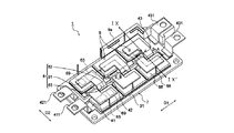
(第1の実施形態)
図1は、第1の実施形態を示す半導体モジュール1の斜視図である。図2Aは、第1の
実施形態の半導体モジュール1を示す図1の模式的なII_A−II_A断面図である。
図2Bは、図1の模式的なII_B−II_B断面図である。半導体モジュール1は、例
えば、風力発電システム、太陽光発電システムおよび電車において、インバータ等の電力
変換装置として用いることができるものである。
(First embodiment)
FIG. 1 is a perspective view of a
FIG. 2B is a schematic II_B-II_B sectional view of FIG. 1. The
図1、図2Aおよび図2Bに示すように、第1の実施形態の半導体モジュール1は、下
層から順に、金属層2と絶縁層3とからなる基板7と、正極側、負極側および出力側の導
体41〜43と、導体41あるいは導体43上に半田層5を介して設けられた半導体パッ
ケージ6と、半導体パッケージ6上に半田層5を介して設けられた第3配線8とを備える
。なお、正極側導体41は、第1配線の一例であり、この場合出力側導体43は第2配線
である。あるいは出力側導体43を第1配線の一例とすると、負極側導体42は第2配線
である。
As shown in FIGS. 1, 2A, and 2B, the
図3は、図1に示す半導体パッケージ6の斜視図である。図4Aは、図3に示す半導体
パッケージ6のIV_A−IV_A断面を示している。図4Aに示すように、半導体パッ
ケージ6は、第1の部材61と、半田層5を介して第1の部材61上に設けられたIGB
T(Insulated gate bipolar transistor)63と、半田層5を介してIGBT63上に
設けられた第2の部材65とを備える。半導体パッケージ6は、表面実装型であり、第1
の部材61と第2の部材65はそれぞれ電極を構成する。なお、IGBT63は、第1の
半導体チップの一例であるが、第1の半導体チップとしてMOSFETやダイオード等の
他の半導体チップを用いてもよい。半導体パッケージ6は、リードフレーム66と、半導
体パッケージ63とリードフレーム66とを接続するボンディングワイヤ67と、封止部
材の一例である封止樹脂68とを備える。
FIG. 3 is a perspective view of the
A T (Insulated gate bipolar transistor) 63 and a
The
図4Bは、図3に示す半導体パッケージ6のIV_B−IV_B断面を示している。具
体的には、半導体パッケージ6は、第1の部材61と、半田層5を介して第1の部材61
上に設けられたダイオード69と、半田層5を介してダイオード69上に設けられた第4
の部材613とを備える。なお、ダイオード69は、第2の半導体チップの一例であるが
、第2の半導体チップとしてMOSFETやIGBT等の他の半導体チップを用いてもよ
い。
FIG. 4B shows a cross section taken along the line IV_B-IV_B of the
The
図4Aと図4Bに示すように、第1の部材61、第2の部材65、第4の部材613は
半導体パッケージ63から露出した部分を有している。この露出した部分は、導体41、
43あるいは第3配線8に半田層5を介して接続している。
As shown in FIGS. 4A and 4B, the
43 or the
図1に示すように、半導体モジュール1は、外囲器の一例として、基板7の外周縁に沿
った枠状のケース9を備える。ケース9は、基板7を支持し、基板7の側部を覆うように
設けられている。なお、図1には、ケース9の一部が図示されている。ケース9の上端9
aは、第3配線8よりも上方に位置する。基板7上のケース9で囲まれた領域は、不図示
の樹脂で封止されている。ケース9の上部は、蓋で覆われていてもよい。
As shown in FIG. 1, the
a is located above the
以下、半導体モジュール1の上記各構成部について詳述する。
The above-mentioned components of the
(基板7)
図1に示すように、基板7は、略矩形状を有する。基板7は、方向D1において長く、
方向D1に略垂直な方向D2において短い。以下、D1を、半導体モジュール1の全長方
向と定義し、D2を、半導体モジュール1の幅方向と定義する。
(Substrate 7)
As shown in FIG. 1, the substrate 7 has a substantially rectangular shape. The substrate 7 is long in the direction D1,
Short in the direction D2 which is substantially perpendicular to the direction D1. Hereinafter, D1 is defined as the entire length direction of the
図1に示すように、基板7は、複数の半導体パッケージ6を配置可能な面積を有する。
図1の例では、基板7上に、全長方向D1に沿って3列、幅方向D2に沿って2列の計6
つの半導体パッケージ6を配置できる。
As shown in FIG. 1, the substrate 7 has an area in which a plurality of
In the example of FIG. 1, a total of 6 rows on the substrate 7 are arranged in three rows along the full length direction D1 and two rows along the width direction D2.
One
基板7を構成する金属層2は、主成分として銅を含有する。従って主成分としてアルミ
ナを含有する場合と比較してコストを削減できる。なお、金属層2は、主成分としてアル
ミニウムを含有してもよい。また、金属層2は、主成分として金属およびセラミック(例
えば、アルミ炭化ケイ素複合材)を含有してもよい。
The
図2Aに示すように、基板7を構成する絶縁層3は、金属層2の上面の全領域に接触し
ている。絶縁層3は、樹脂を含有する。
As shown in FIG. 2A, the insulating
絶縁層3は、好ましくは、フィラーを含有する。フィラーは、例えば、窒化ホウ素、ア
ルミナ、窒化アルミ、窒化ケイ素および炭化ケイ素などであってもよい。
The insulating
絶縁層3は、例えば、8W/mK以上の熱伝導率を有し、フィラーを含有することで、
熱抵抗を低減できる。絶縁層3は、17kV/mm以上の絶縁耐圧を有していてもよい。
金属層2と絶縁層3とで構成された基板7を用いることで、セラミック板を用いる従来の
場合と比較してコストを削減できる。また基板7は放熱の機能を有し、かつ半導体モジュ
ールの支持基板としての役割を果たす。つまり従来の金属ベース基板の機能を兼ね備える
。よって、本実施形態においては、従来用いていた金属ベース基板は不要となる。
The insulating
The thermal resistance can be reduced. The insulating
By using the substrate 7 composed of the
(導体41〜43)
図2Aおよび図2Bに示すように、導体41〜43は、いずれも絶縁層3の上面31に
接して設けられており、配線として用いられる。
(Conductors 41-43)
As shown in FIGS. 2A and 2B, the
図1に示すように、正極側導体41は、全長方向D1に延びている。正極側導体41の
一端には、正極端子411が接続されている。正極側導体41の幅方向D2の寸法は、半
導体パッケージ6の幅方向D2の寸法と程同一である。正極側導体41上には、全長方向
D1に間隔を空けて3つの半導体パッケージ6が配置されている。
As shown in FIG. 1, the positive
出力側導体43は、正極側導体41に対して幅方向D2に間隔を空けて全長方向D1に
延びている。出力側導体43の一端には、2つの出力端子431が接続されている。出力
側導体43上には、全長方向D1に間隔を空けて3つの半導体パッケージ6が配置されて
いる。出力側導体43上の半導体パッケージ6は、正極側導体41上の半導体パッケージ
6に対向している。
The
負極側導体42は、正極側導体41と出力側導体43との間に配置され、全長方向D1
に延びている。負極側導体42の一端には、負極端子421が接続されている。負極側導
体42の幅方向D2の寸法は、正極側導体41および出力側導体43の幅方向D2の寸法
よりも小さい。負極側導体42には、第3配線8が接続されている。
The negative
Extends to. A
導体41〜43は、例えば、主成分として金属を含有し、好ましくは、主成分として銅
を含有する。よって導体41〜43は、導電性を確保しつつ熱抵抗を低減できる。
The
(半導体パッケージ6)
(第1の部材61)
正極側導体41上の半導体パッケージ6の第1の部材61と、出力側導体43上の半導
体パッケージ6の第1の部材61とは、ともに基板7に平行な略矩形の板形状を有する。
第1の部材61は、導電性および熱伝導性を有し、例えば、主成分として金属を含有し、
好ましくは、主成分として銅を含有する。
(Semiconductor package 6)
(First member 61)
The
The
Preferably, copper is contained as the main component.
図2Aに示すように、正極側の第1の部材61は、半田層5を介して正極側導体41と
電気的かつ機械的に接続されている。半田層5は、導電性および熱伝導性を有する。なお
、正極側の第1の部材61は、金属を主成分とする材料を介して正極側導体41と電気的
かつ機械的に接続されていてもよい。
As shown in FIG. 2A, the
図2Bに示すように、出力側の第1の部材61は、半田層5を介して出力側導体43と
電気的かつ機械的に接続されている。なお、出力側の第1の部材61は、金属を主成分と
する材料を介して出力側導体43と電気的かつ機械的に接続されていてもよい。
As shown in FIG. 2B, the output-side
(IGBT63)
図2Aおよび図2Bに示すように、IGBT63は、半田層5を介して第1の部材61
と電気的かつ機械的に接続されている。より具体的には、IGBT63の下面には図示し
ないコレクタ電極が設けられており、コレクタ電極は第1の部材61と接続されている。
また、IGBT63の上面には、図示しないエミッタ電極およびゲート電極が設けられて
いる。図4Aに示すように、ボンディングワイヤ67の一端はゲート電極に接続され、他
端は、リードフレーム66に接続されている。
(IGBT63)
As shown in FIGS. 2A and 2B, the
Is electrically and mechanically connected to. More specifically, a collector electrode (not shown) is provided on the lower surface of the
Further, an emitter electrode and a gate electrode (not shown) are provided on the upper surface of the
(第2の部材65)
図2A、図2Bおよび図3に示すように、第2の部材65は、基板7に平行な略矩形の
板形状を有する。第2の部材65は、導電性および熱伝導性を有し、主成分として金属を
含有し、好ましくは、主成分として銅を含有する。
(Second member 65)
As shown in FIGS. 2A, 2B and 3, the
第2の部材65は、IGBT63上面に半田層5で電気的かつ機械的に接続されている
。より具体的には、第2の部材65は、IGBT63のエミッタ電極と接続されている。
The
従って第2の部材65は、IGBT63で発生した熱を上方に逃がすことができる。
Therefore, the
(ダイオード69側の構成部)
図2Aおよび図2Bに示すように、ダイオード69は、半田層5で第1の部材61と電
気的かつ機械的に接続されている。ダイオード69の下面には図示しないアノード電極が
設けられており、ダイオード69は、アノード電極において第1の部材61と接続されて
いる。
(Structure of
As shown in FIGS. 2A and 2B, the
図2A、図2Bおよび図3に示すように、第4の部材613は、基板7に平行な略矩形
の板形状を有し、例えば、主成分として金属を含有し、好ましくは、主成分として銅を含
有する。第4の部材613は、半田層5でダイオード69と電気的かつ機械的に接続され
ている。より具体的には、ダイオード69の上面には図示しないカソード電極が設けられ
ており、カソード電極は第4の部材613と接続されている。
As shown in FIG. 2A, FIG. 2B, and FIG. 3, the
封止樹脂68は、IGBT63側の積層構造と、ダイオード69側の積層構造とを封止
する。第1の部材61の少なくとも一部、例えば下面は封止樹脂68から露出し、また、
IGBT63の上部に設けられた第2の部材65の少なくとも一部、例えば上面は封止樹
脂68から露出している。これにより、半導体パッケージ6は、上面および下面において
放熱できる。同様に、第4の部材613の少なくとも一部、例えば上面は封止樹脂68か
ら露出している。なお、封止樹脂68は、トランスファーモールド成形で形成している。
The sealing
At least a part of the
図1に示すように、正極側導体41上の半導体パッケージ6は、IGBT63がダイオ
ード69よりも正極端子411側に位置するように金属層2上に配置されている。一方、
出力側導体43上の半導体パッケージ6は、ダイオード69がIGBT63よりも負極端
子421側に位置するように金属層2上に配置されている。すなわち、正極側導体41上
の半導体パッケージ6のIGBT63は、出力側導体43上の半導体パッケージ6のダイ
オード69に対向するように設けられている。
As shown in FIG. 1, the
The
なお、半導体パッケージ6の具体的な態様は、図4Aおよび図4Bに示した態様に限定
されない。半導体パッケージ6は、IGBT63以外の半導体チップを備えていてもよい
。例えば、SiCチップやGaNチップを備えていてもよい。また、半導体パッケージ6
において、ダイオード69を削除することもできる。
The specific form of the
In, the
(第3配線8)
図1に示すように、第3配線8は、平面視において略L字形状であり、半導体パッケー
ジ6の上面に露出した第2の部材65と第4の部材613とに接続する第1の部分81と
、負極側導体42に接続する第2の部分82と、第1の部分81と第2の部分82とを接
続する第3の部分83を有する。なお、パッケージ6中にダイオード69を設けない場合
、第3配線8は、略L字形状でなくてもよい。
(Third wiring 8)
As shown in FIG. 1, the
図2Aおよび図2Bに示すように、第1の部分81は、基板7に平行な板形状を有し、
第4の部材613の上面から第2の部材65の上面に亘るように全長方向D1に延びてい
る。また、第2の部材65上から導体42の方向、すなわち幅方向D2の内方に延びてL
字形状を有している。第1の部分81は、半田層5を介して第2の部材65および第4の
部材613と電気的かつ機械的に接続されている。より具体的には、第1の部分81は、
第2の部材65の上面と第4の部材613の上面の全範囲に接続されており、幅方向D2
において第2の部材65および第4の部材613の幅より大きい幅を有する。なお、第1
の部分81は、金属を主成分とする材料を介して第2の部材65および第4の部材613
と電気的かつ機械的に接続されていてもよい。
As shown in FIGS. 2A and 2B, the
It extends in the entire length direction D1 from the upper surface of the
It has a letter shape. The
It is connected to the entire range of the upper surface of the
In, the width is larger than the widths of the
The
May be electrically and mechanically connected to.
第3の部分83は、第1の部分81の幅方向D2の内端から幅方向D2内方かつ下方に
延びている。すなわち、第3の部分83は、第1の部分81に対して下方に傾斜している
。
The
図2Aに示すように、正極側導体41上の半導体パッケージ6に接続された第3の部分
83(以下、正極側の第3の部分83ともいう)は、その下端部が出力側導体43の近傍
に至る。
As shown in FIG. 2A, the
図2Bに示すように、出力側導体43上の半導体パッケージ6に接続された第3の部分
83(以下、出力側の第3の部分83ともいう)は、その下端部が負極側導体42の近傍
に至る。
As shown in FIG. 2B, the
第2の部分82は、基板7に平行な板形状を有する。図2Aに示すように、正極側の第
3配線8の第2の部分82(以下、正極側の第2の部分82ともいう)は、正極側の第3
の部分83の下端部に繋がっている。正極側の第2の部分82は、半田層5で出力側導体
43と電気的かつ機械的に接続されている。より具体的には、正極側の第2の部分82は
、その底面の全範囲において出力側導体43と接続されている。なお、正極側の第2の部
分82は、金属を主成分とする材料を介して出力側導体43と電気的かつ機械的に接続さ
れていてもよい。
The
Is connected to the lower end of the
図2Bに示すように、出力側の第3配線8の第2の部分82(以下、出力側の第2の部
分82ともいう)は、出力側の第3の部分83の下端部に繋がっている。出力側の第2の
部分82は、半田層5で負極側導体42と電気的かつ機械的に接続されている。より具体
的には、出力側の第2の部分82は、その底面の全範囲において負極側導体42と接続さ
れている。なお、出力側の第2の部分82は、金属を主成分とする材料を介して負極側導
体42と電気的かつ機械的に接続されていてもよい。
As shown in FIG. 2B, the
熱伝導性を有し、上面の全範囲にわたって第2の部材65と接続され、底面の全範囲に
おいて出力側導体43と接続されていることで、正極側の第3配線8は、第2の部材65
に伝達されたIGBT63の熱を、出力側導体43及び金属層2に効率的に逃がすことが
できる。
It has thermal conductivity, is connected to the
The heat of the
また、熱伝導性を有し、上面の全範囲にわたって第2の部材65と接続され、底面の全
範囲において負極側導体42と接続されていることで、出力側の第3配線8は、第2の部
材65に伝達されたIGBT63の熱を、負極側導体42に効率的に逃がすことができる
。
Further, it has thermal conductivity, is connected to the
(等価回路)
図5は、第1の実施形態を示す半導体モジュール1の等価回路図である。図5に示すよ
うに、各半導体パッケージ6において、IGBT63とダイオード69とは逆並列に接続
されている。正極端子411に接続されるIGBT63同士は並列接続され、ダイオード
69同士も並列接続されている。また負極端子421に接続されるIGBT63同士は並
列接続され、ダイオード69同士も並列接続されている。正極側導体41上の半導体パッ
ケージ6のIGBT63およびダイオード69と、出力側導体43上の半導体パッケージ
6のIGBT63およびダイオード69とは、正極側の第3配線8を通じて直列接続され
ている。
(Equivalent circuit)
FIG. 5 is an equivalent circuit diagram of the
正極側導体41上の半導体パッケージ6は、例えば、インバータの上アームとして用い
ることができる。出力側導体43上の半導体パッケージ6は、例えば、インバータの下ア
ームとして用いることができる。
The
(半導体モジュール1の放熱)
以上のように構成された半導体モジュール1は、以下のようにしてIGBT63に発生
した熱を放熱できる。
(Heat dissipation of semiconductor module 1)
The
半導体モジュール1をインバータとして動作させる場合、正極端子411および負極端
子421を直流電源の正極および負極にそれぞれ接続する。また、出力端子431を、例
えば、三相電動機のU端子、V端子、W端子に接続する。また、リードフレーム66を、
ゲートへの入力信号を制御する制御装置に接続する。そして、直流電源で正極端子411
と負極端子421との間に直流電力を印加し、ゲートへの入力信号でIGBT63をスイ
ッチング制御することで、直流電力を三相交流電力に変換する。変換された三相交流電力
は、出力端子431から三相電動機に出力する。
When the
It is connected to the control device that controls the input signal to the gate. Then, the
DC power is applied between the
このような半導体モジュール1の動作の過程において、IGBT63は、スイッチング
制御されることで発熱する。
In the process of the operation of the
図2Aに示すように、正極側導体41上の半導体パッケージ6のIGBT63の下方に
は、順に、半田層5、第1の部材61、半田層5、正極側導体41および絶縁層3を経由
して金属層2に通じる放熱経路が形成されている。また、図2Bに示すように、出力側導
体43上の半導体パッケージ6のIGBT63の下方には、順に、半田層5、第1の部材
61、半田層5、出力側導体43および絶縁層3を経由して金属層2に通じる放熱経路が
形成されている。したがって、IGBT63の下方の放熱経路を通じてIGBT63で発
生した熱を下方に放熱できる。
As shown in FIG. 2A, the
さらに、図2Aに示すように、正極側導体41上の半導体パッケージ6のIGBT63
の上方には、順に、半田層5、第2の部材65、半田層5、第3配線8、半田層5、出力
側導体43および絶縁層3を経由して金属層2に通じる放熱経路が形成されている。また
、図2Bに示すように、出力側導体43上の半導体パッケージ6のIGBT63の上方に
は、順に、半田層5、第2の部材65、半田層5、第3配線8、半田層5、負極側導体4
2および絶縁層3を経由して金属層2に通じる放熱経路が形成されている。したがって、
IGBT63の上方の放熱経路を通じてIGBT63で発生した熱を上方にも放熱できる
。
Further, as shown in FIG. 2A, the
A heat radiating path that leads to the
A heat dissipation path is formed which communicates with the
The heat generated in the
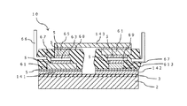
(実験例)
次に、第1の実施形態の実験例について説明する。図6Aは、第1の実施形態の半導体
モジュール1を模擬したシミュレーション用の積層構造100(以下、第1の実施形態の
積層構造ともいう)の断面図である。図6Bは、比較例の半導体モジュールを模擬したシ
ミュレーション用の積層構造200(以下、比較例の積層構造ともいう)の断面図である
。
(Experimental example)
Next, an experimental example of the first embodiment will be described. FIG. 6A is a cross-sectional view of a simulation laminated structure 100 (hereinafter, also referred to as a laminated structure of the first embodiment) simulating the
実験例では、シミュレーションの対象データとして、第1の実施形態の積層構造100
と、比較例の積層構造200とを作成し、両積層構造100、200に対して、以下の条
件で熱伝達シミュレーションを行った。
In the experimental example, as the simulation target data, the
And a
図6Aに示すように、第1の実施形態の積層構造100は、下層から順に、ヒートシン
ク101と、シリコングリス102と、シリコングリス上に設けられ、Cuからなる金属
層103及び樹脂からなる絶縁層104で構成された基板と、Cuからなる導体105と
、半田層106と、Cuからなる部材107と、半田層108と、半導体チップ109と
、半田層110と、Cuからなる部材111と、半田層112と、Cuからなる部材11
3とを備える。Cuからなる金属層103は、金属層2を模擬している。Cuからなる導
体105は、導体41〜43を模擬している。Cuからなる部材107は、第1の部材6
1を模擬している。半導体チップ109は、IGBT63を模擬している。Cuからなる
部材プレート111は、第2の部材65を模擬している。Cuからなる部材113は、第
3配線8を模擬している。
As shown in FIG. 6A, in the
3 and 3. The
I am simulating 1. The
図6Bに示すように、比較例の積層構造200は、下層から順に、ヒートシンク101
と、シリコングリス102と、Cuベース基板103と、半田層201と、Cu層202
と、アルミナ絶縁層203と、Cu配線105と、半田層204と、半導体チップ109
とを備える。
As shown in FIG. 6B, the
,
, The
With.
図7は、第1の実施形態の積層構造100の物性値と、比較例の積層構造200の物性
値とを示す図である。積層構造100、200の各層は、図7に示すような構成材料、成
分および物性値(密度、比熱、熱伝達率)を有する。
FIG. 7 is a diagram showing physical property values of the
シミュレーションでは、積層構造100、200の半導体チップ109が100Wの発
熱量で発熱することを条件とした。また、シミュレーションでは、ヒートシンク101が
400W/m2・Kの冷却能力で半導体チップ109を冷却することを条件とした。
In the simulation, the condition is that the
以上の条件の下でシミュレーションを行った結果、比較例の積層構造200に対して、
第1の実施形態の積層構造100は、熱抵抗を約22%低減できることが確認された。第
1の実施形態の積層構造100は、比較例の積層構造200と異なり、半導体チップ10
9の下層側への放熱経路だけでなく、半導体チップ109の上層側への放熱経路も有して
いるため、熱抵抗を改善できたと推測される。
As a result of performing a simulation under the above conditions, for the
It was confirmed that the
It is presumed that the heat resistance could be improved because not only the heat dissipation path to the lower layer side of the
以上説明したように、第1の実施形態の半導体モジュール1によれば、IGBT63の
上層に第2の部材65と第3配線8とを備えることで、IGBT63の下方への放熱経路
だけでなく、IGBT63の上方への放熱経路も確保できる。これにより、放熱効率を向
上できる。
As described above, according to the
また、第1の実施形態の半導体モジュール1によれば、IGBT63と第1の部材61
及び第2の部材65は、封止樹脂68によって安定的に封止されている。従ってIGBT
63に対し線膨張係数の異なる第1の部材61および第2の部材65は熱変形を生じず、
部材の熱変形に起因したIGBT63の破壊も抑制できる。また、従来構造においてセラ
ミック基板の上面に設けられたCu配線105はエッチングで形成されるため、その厚み
には上限がある。これに対し、本実施形態の第1の部材61および第2の部材65はプレ
ス部品である。従って第1の部材61と第2の部材65の厚みを従来よりも厚くすること
ができる。これにより、IGBT63で発生した過渡熱を、第2および第2の部材61、
65によって迅速に放熱できるので、放熱効率を更に向上できる。
Further, according to the
The
The
The destruction of the
Since heat can be quickly dissipated by 65, the heat dissipation efficiency can be further improved.
また、第1の実施形態の半導体モジュール1によれば、ボンディングワイヤよりも配線
の幅が太い第3配線8を用いることで、インダクタンスを低減できる。
Further, according to the
また、第1の実施形態の半導体モジュール1によれば、IGBT63はダイオード69
よりも第2の部分82の近くに設けられる。従ってIGBT63から第1の部分81乃至
第3の部分83を介して基板7へ向かう熱の伝達距離をダイオード69より短くしている
。これにより、IGBT63からの熱に対する第3配線8の熱抵抗を抑え、放熱効率を向
上できる。また、第3の部分83は、第2の部分82に向かって直進するように傾斜して
いる。これにより、第3配線8中のIGBT63の熱の伝達距離を更に短くすることがで
き、放熱効率を更に向上できる。
In addition, according to the
Is provided closer to the
また、第1の実施形態の半導体モジュール1によれば、図1に示すように、正極側導体
41上の半導体パッケージ6と出力側導体43上の半導体パッケージ6との間で、IGB
T63とダイオード69との相対的な位置関係を互いに逆転させることができる。つまり
、正極側導体41上の半導体パッケージのIGBT63と、出力側導体43上の半導体パ
ッケージ6のダイオード69とが対向して設けられる。これにより、金属層2上のスペー
スにおいて、正極側の第3配線8を出力側の第3配線8に対して180度向きを変えて効
率よく配置する事ができる。
Further, according to the
The relative positional relationship between T63 and the
またIGBTのスイッチングテストを行う場合に、従来では半導体チップ109を実装
したセラミック基板を、金属ベース基板に実装した状態で行う必要があった。これに対し
第1の実施形態の半導体モジュール1は、半導体チップ109がパッケージとして封止さ
れているために、半導体パッケージ6の単位でスイッチングテストを行うことができる。
従って利便性を向上できる。また、信号端子であるリードフレーム66を半導体パッケー
ジ6から直接取り出すことができるので、基板7の金属層2に信号端子を設けることを要
しない。更に半導体パッケージ6はIGBT63を挟んで上下両面に設けられた第1の部
材61と第2の部材65に、厚みが1mm以上のCuからなるプレス部品を用いている。
このような厚みの大きい部材を有する半導体パッケージ6を半導体モジュール1に組み込
むことができるため、IGBT63から効率的に放熱を行うことができる。つまり、半導
体パッケージ6を組み込むことで半導体モジュール1は従来に比べ効率的に放熱を行うこ
とが可能になる。
Further, when performing the switching test of the IGBT, conventionally, it was necessary to perform the test with the ceramic substrate on which the
Therefore, convenience can be improved. Further, since the
Since the
(第2の実施形態)
次に、第2の実施形態について、第1の実施形態との相違点を中心に説明する。図8は
、第2の実施形態を示す半導体モジュール1の断面図である。図8は、図4Aに対応する
断面図であり、正極側導体41上の半導体パッケージ6およびその周辺の構成を示してい
る。
(Second embodiment)
Next, the second embodiment will be described focusing on the differences from the first embodiment. FIG. 8 is a cross-sectional view of the
図8に示すように、第2の実施形態において、第2の部材65と第3配線8の第1の部
分81とは、半田層を介さず超音波接合により直接接続されている。
As shown in FIG. 8, in the second embodiment, the
また、第3配線8の第2の部分82と出力側導体43とは、半田層を介さず超音波接合
により直接接続されている。
The
なお、図示はしないが、出力側導体43上の半導体パッケージ6において、第2の部材
65と第1の部分81とを超音波接続で直接繋げ、第2の部分82と負極側導体42とを
超音波接続で直接繋げてもよい。また、正極側の第1の部材61は、半田層を介さず超音
波接合により直接、正極側導体41と電気的かつ機械的に接続されていてもよい。また、
出力側の第1の部材61も、半田層を介さず超音波接合により直接、出力側導体43と電
気的かつ機械的に接続されていてもよい。
Although not shown, in the
The output-side
第2の実施形態においても、第1の実施形態と同様の効果を有する。特に、半導体モジ
ュール1の放熱効率を向上できる。
The second embodiment also has the same effect as that of the first embodiment. In particular, the heat dissipation efficiency of the
(第3の実施形態)
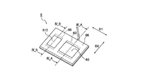
次に、第3の実施形態について、第1の実施形態との相違点を中心に説明する。図9は
、図1に示す第1の実施形態の半導体モジュール1のIX−IX’断面を示している。図
10は、第3の実施形態の半導体モジュール10断面図である。図10は、図9に対応す
る断面図であり、半導体パッケージ6と導体141、142、143との構成を示してい
る。なお、正極側導体141は、第4配線、負極側導体142は第5配線、出力側導体1
43は第6配線である。
(Third Embodiment)
Next, the third embodiment will be described focusing on the differences from the first embodiment. FIG. 9 shows a IX-IX ′ cross section of the
第1の実施形態は、図5で示したように例えばインバータとして動作し、インバータの
上アームと下アームは異なるタイミングでオンとオフのスイッチングを行う。第1の実施
形態の図1に示す構造において、IGBT63のオンからオフへのスイッチング直後に、
サージ電圧が発生する。このサージ電圧が各素子の許容値を超えると素子が破壊される。
サージ電圧ΔVは、インダクタンスL、電流iを用いて以下の式のように表せる。
The first embodiment operates as an inverter, for example, as shown in FIG. 5, and the upper arm and the lower arm of the inverter perform on / off switching at different timings. In the structure shown in FIG. 1 of the first embodiment, immediately after switching the
Surge voltage is generated. When the surge voltage exceeds the allowable value of each element, the element is destroyed.
The surge voltage ΔV can be expressed by the following equation using the inductance L and the current i.
ΔV=L・di/dt・・・(1) ΔV = L · di / dt (1)
高速スイッチング化に伴いサージ電圧ΔVの値が大きくなる。サージ電圧を下げるため
に、インダクタンスLを低減することが重要であり、サージ電圧の発生に関係する電流経
路が短いほどインダクタンスは低減する。このとき、サージ電圧の発生に関係する電流は
、オンからオフへのスイッチング直後にIGBT63に暫く減少しながら流れる電流とダ
イオード69に流れる電流とを合わせて考えたときの電流である。
The value of the surge voltage ΔV increases as the switching speed increases. In order to reduce the surge voltage, it is important to reduce the inductance L, and the shorter the current path related to the generation of the surge voltage, the lower the inductance. At this time, the current related to the generation of the surge voltage is a current when the current flowing in the
第1の実施形態において、サージ電圧の発生に関係する電流経路は順に、正極端子41
1、正極側導体41、正極側導体41に搭載されている半導体パッケージ6、第3配線8
、出力側導体43、出力側導体43に搭載されている半導体パッケージ6、第3配線8、
負極側導体42、負極端子421である。
In the first embodiment, the current paths related to the generation of the surge voltage are sequentially connected to the
1, the positive
An
The negative
これに対し、第3の実施形態では、第3配線8を用いずに半導体モジュールが構成され
る。これにより、サージ電圧の発生に関係する電流経路が短縮される。図10に示すよう
に、半導体モジュール10には、金属層2上に絶縁層3を介して正極側導体141と負極
側導体142が設けられている。正極側導体141と負極側導体142上にはそれぞれ半
導体パッケージ6が設けられている。この一組の半導体パッケージ6上に、すなわち、半
導体パッケージ6の正極側導体141および負極側導体142に接する面と反対側の面に
、出力側導体143が設けられている。出力側導体143は、一組の半導体パッケージ6
の上面全体を覆うように設けられている。正極側導体141上に設けられた半導体パッケ
ージ6において、内部に設けられたIGBTのエミッタ電極は、出力側導体143に向か
い合うよう設けられている。一方、負極側導体142上に設けられた半導体パッケージ6
において、内部に設けられたIGBTのコレクタ電極は、出力側導体143に向かい合う
よう設けられている。つまり、負極側導体142上の半導体パッケージ6は、正極側導体
141上の半導体パッケージに対して上下反転して設置されている。以上より、半導体モ
ジュール10は、第3の配線8を不要とする。
On the other hand, in the third embodiment, the semiconductor module is configured without using the
Is provided so as to cover the entire upper surface of the. In the
In, the collector electrode of the IGBT provided inside is provided so as to face the output side conductor 143. That is, the
半導体モジュール10においてサージ電圧の発生に関係する電流経路は順に、正極端子
411、正極側導体141、正極側導体141に搭載されている半導体パッケージ6、出
力側導体143、負極側導体142に搭載されている半導体パッケージ6、負極側導体1
42、負極端子421である。つまり、第1の実施形態の半導体モジュール1に対して、
第3の実施形態の半導体モジュール10は、第3の配線8を経由する必要がなくなり、サ
ージ電圧の発生に関係する電流経路を短くすることができる。よって、IGBT63の両
面で放熱する構造を有しながら、インダクタンスの低減を図ることが出来る。
In the
42 and a
The
シミュレーションの結果、第1実施形態に対して第3実施形態のインダクタンスは約2
0%低減することが確認された。
As a result of the simulation, the inductance of the third embodiment is about 2 compared with the first embodiment.
It was confirmed to reduce by 0%.
また、半導体モジュール10において、半導体パッケージ6は、IGBTに加え、ダイ
オードを有している。半導体パッケージ6を形成する場合、IGBTとダイオードを互い
に上下反転させることなく設けることができる。また、このように形成された半導体パッ
ケージ6を用いて半導体モジュール10を形成する場合、上述したとおり、一組の半導体
パッケージ6のうち、一方を他方に対して上下反転させるのみでよく、組み立て性や信頼
性が向上する。また、パッケージサイズも小さくできる。一方、半導体チップ単体を用い
て半導体モジュールを形成する比較例の場合、すなわち、IGBTとダイオードの2つの
半導体チップを他のIGBTとダイオードの2つの半導体チップに対して上下反転して設
ける場合、計4個の半導体チップを半導体モジュール10に設けることになり、第3の実
施形態に比べ組み立て性や信頼性が下がる。また半導体モジュールも大きくなってしまう
。
In the
半導体モジュール10は、金属層2上に絶縁層3を介して正極側導体141と負極側導
体142を設けているが、代わりに出力側導体143を設けても良い。この場合、一組の
半導体パッケージの上面に正極側導体141と負極側導体142がそれぞれ設けられる。
また、上面に負極側導体142を有する半導体パッケージ6は、上面に正極側導体141
を有する半導体パッケージ6に対して上下反転して設置される。この場合も同様に、サー
ジ電圧の発生に関係する電流経路が短縮化される。
In the
In addition, the
Is installed upside down with respect to the
なお、第1から第3の実施形態において、半田層5の替わりに銀ナノペーストを採用し
てもよい。
In the first to third embodiments, silver nanopaste may be used instead of the
本発明のいくつかの実施形態を説明したが、これらの実施形態は、例として提示したも
のであり、発明の範囲を限定することは意図していない。これら実施形態は、その他の様
々な形態で実施されることが可能であり、発明の要旨を逸脱しない範囲で、種々の省略、
置き換え、変更を行うことができる。これら実施形態やその変形は、発明の範囲や要旨に
含まれると同様に、特許請求の範囲に記載された発明とその均等の範囲に含まれるもので
ある。
Although some embodiments of the present invention have been described, these embodiments are presented as examples and are not intended to limit the scope of the invention. These embodiments can be implemented in various other forms, and various omissions can be made without departing from the scope of the invention.
It can be replaced and changed. These embodiments and their modifications are included in the invention described in the claims and the equivalents thereof as well as included in the scope and the gist of the invention.
1 半導体モジュール
2 金属層
3 絶縁層
41 正極側導体
42 負極側導体
43 出力側導体
5 半田層
6 半導体パッケージ
61 第1の部材
63 IGBT
65 第2の部材
66 リードフレーム
68 封止樹脂
69 ダイオード
7 基板
8 第3配線
81 第1の部分
82 第2の部分
83 第3の部分
9 ケース
10 半導体モジュール
141 正極側導体
142 負極側導体
143 出力側導体
1
65
69 diode 7
Claims (6)
前記基板上に設けられた第6配線と、
前記第6配線上に設けられ、上部および下部において放熱する第1半導体パッケージと
、
前記第6配線上に、前記第1半導体パッケージに対して上下反転して設けられ、上部お
よび下部において放熱する第2半導体パッケージと、
前記第1半導体パッケージ上に設けられた第4配線と、
前記第2半導体パッケージ上に設けられた第5配線と、を備え、
前記第1半導体パッケージと前記第2半導体パッケージは前記第6配線を介して、直列
接続される半導体モジュール。 A substrate having a metal layer and an insulating layer provided on the metal layer and containing a resin;
A sixth wiring provided on the substrate,
A first semiconductor package which is provided on the sixth wiring and radiates heat in an upper portion and a lower portion;
A second semiconductor package, which is provided on the sixth wiring and is turned upside down with respect to the first semiconductor package, and radiates heat in an upper portion and a lower portion;
A fourth wiring provided on the first semiconductor package;
A fifth wiring provided on the second semiconductor package,
A semiconductor module in which the first semiconductor package and the second semiconductor package are connected in series via the sixth wiring.
前記下部に設けられ、導電性および熱伝導性を有する第3の部材と、
前記上部に設けられ、導電性および熱伝導性を有する第4の部材と、
前記第3の部材と前記第4の部材との間に設けられた第2の半導体チップと、
前記第3の部材と前記第4の部材と前記第2の半導体チップとを封止する封止部材と、
を備える請求項1に記載の半導体モジュール。 The second semiconductor package is
A third member provided on the lower portion and having electrical conductivity and thermal conductivity;
A fourth member provided on the upper portion and having electrical conductivity and thermal conductivity;
A second semiconductor chip provided between the third member and the fourth member;
A sealing member that seals the third member, the fourth member, and the second semiconductor chip;
The semiconductor module according to claim 1 , further comprising:
前記第1半導体パッケージの前記下部に設けられ、導電性および熱伝導性を有する第1
の部材と、
前記第1半導体パッケージの前記上部に設けられ、導電性および熱伝導性を有する第2
の部材と、
前記第1の部材と前記第2の部材との間に設けられた第1の半導体チップと、
前記第1の部材と前記第2の部材と前記第1の半導体チップとを封止する封止部材と、
を備える請求項1から2のいずれかに記載の半導体モジュール。 The first semiconductor package is
A first semiconductor package provided under the first semiconductor package and having electrical conductivity and thermal conductivity;
Members of
A second semiconductor package provided on the upper portion of the first semiconductor package and having electrical conductivity and thermal conductivity;
Members of
A first semiconductor chip provided between the first member and the second member;
A sealing member that seals the first member, the second member, and the first semiconductor chip;
The semiconductor module according to claim 1, further comprising:
、前記第2の部材は半田あるいは金属を主成分とする材料を介して前記第6配線に接続す
る請求項3に記載の半導体モジュール。 The first member is connected to the fourth wiring via a material containing solder or metal as a main component, and the second member is connected to the sixth wiring via a material containing solder or metal as a main component. The semiconductor module according to claim 3 .
続する請求項3に記載の半導体モジュール。 The semiconductor module according to claim 3 , wherein the first member is directly connected to the fourth wiring, and the second member is directly connected to the sixth wiring.
面全体に接して設けられる請求項3に記載の半導体モジュール。 The semiconductor module according to claim 3 , wherein the second member has an exposed surface exposed from the sealing member, and the sixth wiring is provided in contact with the entire exposed surface.
Applications Claiming Priority (2)
| Application Number | Priority Date | Filing Date | Title |
|---|---|---|---|
| JP2015233751 | 2015-11-30 | ||
| JP2015233751 | 2015-11-30 |
Publications (3)
| Publication Number | Publication Date |
|---|---|
| JP2017108130A JP2017108130A (en) | 2017-06-15 |
| JP2017108130A5 JP2017108130A5 (en) | 2019-03-22 |
| JP6685884B2 true JP6685884B2 (en) | 2020-04-22 |
Family
ID=58777338
Family Applications (1)
| Application Number | Title | Priority Date | Filing Date |
|---|---|---|---|
| JP2016231244A Active JP6685884B2 (en) | 2015-11-30 | 2016-11-29 | Semiconductor module |
Country Status (2)
| Country | Link |
|---|---|
| US (1) | US10217690B2 (en) |
| JP (1) | JP6685884B2 (en) |
Families Citing this family (8)
| Publication number | Priority date | Publication date | Assignee | Title |
|---|---|---|---|---|
| WO2018008424A1 (en) * | 2016-07-08 | 2018-01-11 | 三菱電機株式会社 | Semiconductor device and power conversion device |
| WO2018020729A1 (en) * | 2016-07-27 | 2018-02-01 | 株式会社日立製作所 | Semiconductor module and method for manufacturing semiconductor module |
| JP6891904B2 (en) * | 2017-02-06 | 2021-06-18 | 富士電機株式会社 | Semiconductor modules, electric vehicles and power control units |
| JP6470328B2 (en) * | 2017-02-09 | 2019-02-13 | 株式会社東芝 | Semiconductor module |
| US11183479B2 (en) * | 2017-03-30 | 2021-11-23 | Mitsubishi Electric Corporation | Semiconductor device, method for manufacturing the same, and power conversion device |
| TWI675441B (en) * | 2018-05-14 | 2019-10-21 | 欣興電子股份有限公司 | Package carrier structure and manufacturing method thereof |
| JP7301805B2 (en) * | 2020-09-24 | 2023-07-03 | 株式会社東芝 | semiconductor module |
| JP7354076B2 (en) | 2020-09-24 | 2023-10-02 | 株式会社東芝 | semiconductor module |
Family Cites Families (19)
| Publication number | Priority date | Publication date | Assignee | Title |
|---|---|---|---|---|
| WO1998008256A1 (en) * | 1996-08-20 | 1998-02-26 | Kabushiki Kaisha Toshiba | Silicon nitride circuit board and semiconductor module |
| JP2006511085A (en) * | 2002-12-20 | 2006-03-30 | コーニンクレッカ フィリップス エレクトロニクス エヌ ヴィ | Electronic device and manufacturing method thereof |
| JP2004241734A (en) * | 2003-02-10 | 2004-08-26 | Toyota Industries Corp | Semiconductor module |
| JP2005109100A (en) * | 2003-09-30 | 2005-04-21 | Mitsubishi Electric Corp | Semiconductor device and manufacturing method thereof |
| JP2006080153A (en) * | 2004-09-07 | 2006-03-23 | Toshiba Corp | Semiconductor device |
| JP4770533B2 (en) | 2005-05-16 | 2011-09-14 | 富士電機株式会社 | Semiconductor device manufacturing method and semiconductor device |
| JP4775327B2 (en) * | 2007-06-06 | 2011-09-21 | 富士電機株式会社 | Manufacturing method of semiconductor device |
| US8138587B2 (en) * | 2008-09-30 | 2012-03-20 | Infineon Technologies Ag | Device including two mounting surfaces |
| JP2011086889A (en) * | 2009-10-19 | 2011-04-28 | Renesas Electronics Corp | Semiconductor device and manufacturing method thereof |
| US8120158B2 (en) * | 2009-11-10 | 2012-02-21 | Infineon Technologies Ag | Laminate electronic device |
| JP5253455B2 (en) * | 2010-06-01 | 2013-07-31 | 三菱電機株式会社 | Power semiconductor device |
| JP5520889B2 (en) * | 2011-06-24 | 2014-06-11 | 日立オートモティブシステムズ株式会社 | Power semiconductor module and power converter using the same |
| JP5706251B2 (en) * | 2011-06-30 | 2015-04-22 | ルネサスエレクトロニクス株式会社 | Semiconductor device |
| JP5863602B2 (en) | 2011-08-31 | 2016-02-16 | 三菱電機株式会社 | Power semiconductor device |
| JP2013097560A (en) | 2011-10-31 | 2013-05-20 | Mitsubishi Heavy Ind Ltd | System for optimizing process of construction work and method for optimizing process of construction work |
| JP5965687B2 (en) | 2012-03-23 | 2016-08-10 | 株式会社 日立パワーデバイス | Power semiconductor module |
| JP2014157927A (en) * | 2013-02-15 | 2014-08-28 | Denso Corp | Semiconductor device and manufacturing method of the same |
| JP2015095560A (en) * | 2013-11-12 | 2015-05-18 | 株式会社デンソー | Power module |
| JP2015144188A (en) * | 2014-01-31 | 2015-08-06 | 株式会社東芝 | Semiconductor device and manufacturing method of the same |
-
2016
- 2016-08-04 US US15/228,086 patent/US10217690B2/en active Active
- 2016-11-29 JP JP2016231244A patent/JP6685884B2/en active Active
Also Published As
| Publication number | Publication date |
|---|---|
| US20170154834A1 (en) | 2017-06-01 |
| US10217690B2 (en) | 2019-02-26 |
| JP2017108130A (en) | 2017-06-15 |
Similar Documents
| Publication | Publication Date | Title |
|---|---|---|
| JP6685884B2 (en) | Semiconductor module | |
| EP3107120B1 (en) | Power semiconductor module | |
| US8987777B2 (en) | Stacked half-bridge power module | |
| JP4803241B2 (en) | Semiconductor module | |
| KR101388737B1 (en) | Semiconductor package, semiconductor module, and mounting structure thereof | |
| US10084389B2 (en) | Power module | |
| JP6786416B2 (en) | Semiconductor device | |
| JP6852011B2 (en) | Semiconductor device | |
| JP2015095560A (en) | Power module | |
| US8823153B2 (en) | Semiconductor package | |
| JP2021141222A (en) | Semiconductor module | |
| US10896864B2 (en) | Power semiconductor chip module | |
| US11081412B2 (en) | Semiconductor device | |
| JP2013125889A (en) | Semiconductor device | |
| JP4375299B2 (en) | Power semiconductor device | |
| JP6156131B2 (en) | Semiconductor device | |
| JP2009117701A (en) | Power module | |
| JP6305362B2 (en) | Power semiconductor module | |
| US10658344B2 (en) | Semiconductor device | |
| JP2017069351A (en) | Semiconductor device | |
| JP2013098343A (en) | Semiconductor device and method of manufacturing the same | |
| JP5444486B2 (en) | Inverter device | |
| JP6884723B2 (en) | Semiconductor device | |
| JP2010171463A (en) | Power semiconductor device and inverter device using the same | |
| JP5494576B2 (en) | Semiconductor module |
Legal Events
| Date | Code | Title | Description |
|---|---|---|---|
| A711 | Notification of change in applicant |
Free format text: JAPANESE INTERMEDIATE CODE: A711 Effective date: 20170929 Free format text: JAPANESE INTERMEDIATE CODE: A712 Effective date: 20170929 |
|
| RD03 | Notification of appointment of power of attorney |
Free format text: JAPANESE INTERMEDIATE CODE: A7423 Effective date: 20180831 |
|
| A521 | Request for written amendment filed |
Free format text: JAPANESE INTERMEDIATE CODE: A523 Effective date: 20190204 |
|
| A621 | Written request for application examination |
Free format text: JAPANESE INTERMEDIATE CODE: A621 Effective date: 20190204 |
|
| A977 | Report on retrieval |
Free format text: JAPANESE INTERMEDIATE CODE: A971007 Effective date: 20191030 |
|
| A131 | Notification of reasons for refusal |
Free format text: JAPANESE INTERMEDIATE CODE: A131 Effective date: 20191206 |
|
| A521 | Request for written amendment filed |
Free format text: JAPANESE INTERMEDIATE CODE: A523 Effective date: 20200204 |
|
| TRDD | Decision of grant or rejection written | ||
| A01 | Written decision to grant a patent or to grant a registration (utility model) |
Free format text: JAPANESE INTERMEDIATE CODE: A01 Effective date: 20200306 |
|
| A61 | First payment of annual fees (during grant procedure) |
Free format text: JAPANESE INTERMEDIATE CODE: A61 Effective date: 20200401 |
|
| R150 | Certificate of patent or registration of utility model |
Ref document number: 6685884 Country of ref document: JP Free format text: JAPANESE INTERMEDIATE CODE: R150 |