JP6678506B2 - Semiconductor package and method of manufacturing semiconductor package - Google Patents
Semiconductor package and method of manufacturing semiconductor package Download PDFInfo
- Publication number
- JP6678506B2 JP6678506B2 JP2016090189A JP2016090189A JP6678506B2 JP 6678506 B2 JP6678506 B2 JP 6678506B2 JP 2016090189 A JP2016090189 A JP 2016090189A JP 2016090189 A JP2016090189 A JP 2016090189A JP 6678506 B2 JP6678506 B2 JP 6678506B2
- Authority
- JP
- Japan
- Prior art keywords
- semiconductor device
- insulating layer
- resin insulating
- opening
- recess
- Prior art date
- Legal status (The legal status is an assumption and is not a legal conclusion. Google has not performed a legal analysis and makes no representation as to the accuracy of the status listed.)
- Active
Links
- 239000004065 semiconductor Substances 0.000 title claims description 279
- 238000004519 manufacturing process Methods 0.000 title claims description 97
- 239000010410 layer Substances 0.000 claims description 208
- 239000011347 resin Substances 0.000 claims description 126
- 229920005989 resin Polymers 0.000 claims description 126
- 238000000034 method Methods 0.000 claims description 73
- 239000012790 adhesive layer Substances 0.000 claims description 59
- 239000000463 material Substances 0.000 claims description 55
- 239000000758 substrate Substances 0.000 claims description 54
- 239000004020 conductor Substances 0.000 claims description 3
- 239000003550 marker Substances 0.000 description 120
- 229910000679 solder Inorganic materials 0.000 description 29
- 238000005530 etching Methods 0.000 description 21
- 239000010408 film Substances 0.000 description 19
- 229920002120 photoresistant polymer Polymers 0.000 description 17
- 238000007747 plating Methods 0.000 description 16
- 239000010949 copper Substances 0.000 description 12
- 239000000945 filler Substances 0.000 description 11
- 229910052751 metal Inorganic materials 0.000 description 11
- 239000002184 metal Substances 0.000 description 11
- 239000000126 substance Substances 0.000 description 10
- 238000009832 plasma treatment Methods 0.000 description 9
- KDLHZDBZIXYQEI-UHFFFAOYSA-N Palladium Chemical compound [Pd] KDLHZDBZIXYQEI-UHFFFAOYSA-N 0.000 description 7
- 238000007772 electroless plating Methods 0.000 description 7
- 238000007788 roughening Methods 0.000 description 7
- 238000000206 photolithography Methods 0.000 description 6
- PXHVJJICTQNCMI-UHFFFAOYSA-N Nickel Chemical compound [Ni] PXHVJJICTQNCMI-UHFFFAOYSA-N 0.000 description 5
- 229910052802 copper Inorganic materials 0.000 description 5
- 239000003822 epoxy resin Substances 0.000 description 5
- 239000007788 liquid Substances 0.000 description 5
- 229920000647 polyepoxide Polymers 0.000 description 5
- 238000005520 cutting process Methods 0.000 description 4
- 238000010586 diagram Methods 0.000 description 4
- 238000009713 electroplating Methods 0.000 description 4
- 238000009413 insulation Methods 0.000 description 4
- 230000003472 neutralizing effect Effects 0.000 description 4
- 239000011135 tin Substances 0.000 description 4
- LYCAIKOWRPUZTN-UHFFFAOYSA-N Ethylene glycol Chemical compound OCCO LYCAIKOWRPUZTN-UHFFFAOYSA-N 0.000 description 3
- 239000011651 chromium Substances 0.000 description 3
- 238000010438 heat treatment Methods 0.000 description 3
- 230000001678 irradiating effect Effects 0.000 description 3
- 229910052759 nickel Inorganic materials 0.000 description 3
- 239000003960 organic solvent Substances 0.000 description 3
- 229910052763 palladium Inorganic materials 0.000 description 3
- 238000005240 physical vapour deposition Methods 0.000 description 3
- BASFCYQUMIYNBI-UHFFFAOYSA-N platinum Chemical compound [Pt] BASFCYQUMIYNBI-UHFFFAOYSA-N 0.000 description 3
- 229910052709 silver Inorganic materials 0.000 description 3
- 238000004528 spin coating Methods 0.000 description 3
- 230000008961 swelling Effects 0.000 description 3
- JYLNVJYYQQXNEK-UHFFFAOYSA-N 3-amino-2-(4-chlorophenyl)-1-propanesulfonic acid Chemical compound OS(=O)(=O)CC(CN)C1=CC=C(Cl)C=C1 JYLNVJYYQQXNEK-UHFFFAOYSA-N 0.000 description 2
- RYGMFSIKBFXOCR-UHFFFAOYSA-N Copper Chemical compound [Cu] RYGMFSIKBFXOCR-UHFFFAOYSA-N 0.000 description 2
- YCKRFDGAMUMZLT-UHFFFAOYSA-N Fluorine atom Chemical compound [F] YCKRFDGAMUMZLT-UHFFFAOYSA-N 0.000 description 2
- VYPSYNLAJGMNEJ-UHFFFAOYSA-N Silicium dioxide Chemical compound O=[Si]=O VYPSYNLAJGMNEJ-UHFFFAOYSA-N 0.000 description 2
- 229910001128 Sn alloy Inorganic materials 0.000 description 2
- QAOWNCQODCNURD-UHFFFAOYSA-N Sulfuric acid Chemical compound OS(O)(=O)=O QAOWNCQODCNURD-UHFFFAOYSA-N 0.000 description 2
- 230000001070 adhesive effect Effects 0.000 description 2
- 229910052782 aluminium Inorganic materials 0.000 description 2
- XAGFODPZIPBFFR-UHFFFAOYSA-N aluminium Chemical compound [Al] XAGFODPZIPBFFR-UHFFFAOYSA-N 0.000 description 2
- QVGXLLKOCUKJST-UHFFFAOYSA-N atomic oxygen Chemical compound [O] QVGXLLKOCUKJST-UHFFFAOYSA-N 0.000 description 2
- 230000015572 biosynthetic process Effects 0.000 description 2
- 229910052804 chromium Inorganic materials 0.000 description 2
- 238000000576 coating method Methods 0.000 description 2
- 238000007598 dipping method Methods 0.000 description 2
- 239000011737 fluorine Substances 0.000 description 2
- 229910052731 fluorine Inorganic materials 0.000 description 2
- 239000007789 gas Substances 0.000 description 2
- 239000010931 gold Substances 0.000 description 2
- 230000003287 optical effect Effects 0.000 description 2
- 229910052760 oxygen Inorganic materials 0.000 description 2
- 239000001301 oxygen Substances 0.000 description 2
- 239000002245 particle Substances 0.000 description 2
- -1 polybutylene terephthalate Polymers 0.000 description 2
- 229920001721 polyimide Polymers 0.000 description 2
- 239000012286 potassium permanganate Substances 0.000 description 2
- 239000010948 rhodium Substances 0.000 description 2
- 238000007789 sealing Methods 0.000 description 2
- 239000010944 silver (metal) Substances 0.000 description 2
- 239000002356 single layer Substances 0.000 description 2
- 239000002904 solvent Substances 0.000 description 2
- 239000010409 thin film Substances 0.000 description 2
- 229910052718 tin Inorganic materials 0.000 description 2
- 239000010936 titanium Substances 0.000 description 2
- 238000007740 vapor deposition Methods 0.000 description 2
- 238000005406 washing Methods 0.000 description 2
- XLYOFNOQVPJJNP-UHFFFAOYSA-N water Substances O XLYOFNOQVPJJNP-UHFFFAOYSA-N 0.000 description 2
- ZNBNBTIDJSKEAM-UHFFFAOYSA-N 4-[7-hydroxy-2-[5-[5-[6-hydroxy-6-(hydroxymethyl)-3,5-dimethyloxan-2-yl]-3-methyloxolan-2-yl]-5-methyloxolan-2-yl]-2,8-dimethyl-1,10-dioxaspiro[4.5]decan-9-yl]-2-methyl-3-propanoyloxypentanoic acid Chemical compound C1C(O)C(C)C(C(C)C(OC(=O)CC)C(C)C(O)=O)OC11OC(C)(C2OC(C)(CC2)C2C(CC(O2)C2C(CC(C)C(O)(CO)O2)C)C)CC1 ZNBNBTIDJSKEAM-UHFFFAOYSA-N 0.000 description 1
- 239000004925 Acrylic resin Substances 0.000 description 1
- 229920000178 Acrylic resin Polymers 0.000 description 1
- VYZAMTAEIAYCRO-UHFFFAOYSA-N Chromium Chemical compound [Cr] VYZAMTAEIAYCRO-UHFFFAOYSA-N 0.000 description 1
- 229910021578 Iron(III) chloride Inorganic materials 0.000 description 1
- 229920000106 Liquid crystal polymer Polymers 0.000 description 1
- 239000004977 Liquid-crystal polymers (LCPs) Substances 0.000 description 1
- OAICVXFJPJFONN-UHFFFAOYSA-N Phosphorus Chemical compound [P] OAICVXFJPJFONN-UHFFFAOYSA-N 0.000 description 1
- 239000004696 Poly ether ether ketone Substances 0.000 description 1
- 229930182556 Polyacetal Natural products 0.000 description 1
- 239000004952 Polyamide Substances 0.000 description 1
- 239000004962 Polyamide-imide Substances 0.000 description 1
- 239000004695 Polyether sulfone Substances 0.000 description 1
- 239000004697 Polyetherimide Substances 0.000 description 1
- 239000004642 Polyimide Substances 0.000 description 1
- 239000004721 Polyphenylene oxide Substances 0.000 description 1
- 239000004734 Polyphenylene sulfide Substances 0.000 description 1
- XUIMIQQOPSSXEZ-UHFFFAOYSA-N Silicon Chemical compound [Si] XUIMIQQOPSSXEZ-UHFFFAOYSA-N 0.000 description 1
- BQCADISMDOOEFD-UHFFFAOYSA-N Silver Chemical compound [Ag] BQCADISMDOOEFD-UHFFFAOYSA-N 0.000 description 1
- 229920010524 Syndiotactic polystyrene Polymers 0.000 description 1
- ATJFFYVFTNAWJD-UHFFFAOYSA-N Tin Chemical compound [Sn] ATJFFYVFTNAWJD-UHFFFAOYSA-N 0.000 description 1
- RTAQQCXQSZGOHL-UHFFFAOYSA-N Titanium Chemical compound [Ti] RTAQQCXQSZGOHL-UHFFFAOYSA-N 0.000 description 1
- 238000002679 ablation Methods 0.000 description 1
- 238000010306 acid treatment Methods 0.000 description 1
- 239000000853 adhesive Substances 0.000 description 1
- 229910045601 alloy Inorganic materials 0.000 description 1
- 239000000956 alloy Substances 0.000 description 1
- PNEYBMLMFCGWSK-UHFFFAOYSA-N aluminium oxide Inorganic materials [O-2].[O-2].[O-2].[Al+3].[Al+3] PNEYBMLMFCGWSK-UHFFFAOYSA-N 0.000 description 1
- 229910052787 antimony Inorganic materials 0.000 description 1
- WATWJIUSRGPENY-UHFFFAOYSA-N antimony atom Chemical compound [Sb] WATWJIUSRGPENY-UHFFFAOYSA-N 0.000 description 1
- 239000004760 aramid Substances 0.000 description 1
- 229920003235 aromatic polyamide Polymers 0.000 description 1
- 238000004380 ashing Methods 0.000 description 1
- UMIVXZPTRXBADB-UHFFFAOYSA-N benzocyclobutene Chemical compound C1=CC=C2CCC2=C1 UMIVXZPTRXBADB-UHFFFAOYSA-N 0.000 description 1
- 229910052797 bismuth Inorganic materials 0.000 description 1
- JCXGWMGPZLAOME-UHFFFAOYSA-N bismuth atom Chemical compound [Bi] JCXGWMGPZLAOME-UHFFFAOYSA-N 0.000 description 1
- 239000000919 ceramic Substances 0.000 description 1
- 229910017052 cobalt Inorganic materials 0.000 description 1
- 239000010941 cobalt Substances 0.000 description 1
- GUTLYIVDDKVIGB-UHFFFAOYSA-N cobalt atom Chemical compound [Co] GUTLYIVDDKVIGB-UHFFFAOYSA-N 0.000 description 1
- 239000000084 colloidal system Substances 0.000 description 1
- 150000001875 compounds Chemical class 0.000 description 1
- 238000001816 cooling Methods 0.000 description 1
- XLJMAIOERFSOGZ-UHFFFAOYSA-M cyanate Chemical compound [O-]C#N XLJMAIOERFSOGZ-UHFFFAOYSA-M 0.000 description 1
- 230000007423 decrease Effects 0.000 description 1
- 229910003460 diamond Inorganic materials 0.000 description 1
- 239000010432 diamond Substances 0.000 description 1
- 229940028356 diethylene glycol monobutyl ether Drugs 0.000 description 1
- 238000001312 dry etching Methods 0.000 description 1
- 230000000694 effects Effects 0.000 description 1
- 238000005566 electron beam evaporation Methods 0.000 description 1
- 238000005516 engineering process Methods 0.000 description 1
- 230000006870 function Effects 0.000 description 1
- 229910052732 germanium Inorganic materials 0.000 description 1
- GNPVGFCGXDBREM-UHFFFAOYSA-N germanium atom Chemical compound [Ge] GNPVGFCGXDBREM-UHFFFAOYSA-N 0.000 description 1
- 239000011521 glass Substances 0.000 description 1
- PCHJSUWPFVWCPO-UHFFFAOYSA-N gold Chemical compound [Au] PCHJSUWPFVWCPO-UHFFFAOYSA-N 0.000 description 1
- 229910052737 gold Inorganic materials 0.000 description 1
- FFUAGWLWBBFQJT-UHFFFAOYSA-N hexamethyldisilazane Chemical compound C[Si](C)(C)N[Si](C)(C)C FFUAGWLWBBFQJT-UHFFFAOYSA-N 0.000 description 1
- 230000005661 hydrophobic surface Effects 0.000 description 1
- 229910000378 hydroxylammonium sulfate Inorganic materials 0.000 description 1
- 229910052738 indium Inorganic materials 0.000 description 1
- APFVFJFRJDLVQX-UHFFFAOYSA-N indium atom Chemical compound [In] APFVFJFRJDLVQX-UHFFFAOYSA-N 0.000 description 1
- 239000011256 inorganic filler Substances 0.000 description 1
- 229910003475 inorganic filler Inorganic materials 0.000 description 1
- 229910010272 inorganic material Inorganic materials 0.000 description 1
- 239000011147 inorganic material Substances 0.000 description 1
- 150000002500 ions Chemical class 0.000 description 1
- 229910052742 iron Inorganic materials 0.000 description 1
- XEEYBQQBJWHFJM-UHFFFAOYSA-N iron Substances [Fe] XEEYBQQBJWHFJM-UHFFFAOYSA-N 0.000 description 1
- RBTARNINKXHZNM-UHFFFAOYSA-K iron trichloride Chemical compound Cl[Fe](Cl)Cl RBTARNINKXHZNM-UHFFFAOYSA-K 0.000 description 1
- 239000007769 metal material Substances 0.000 description 1
- 150000002739 metals Chemical class 0.000 description 1
- 239000010445 mica Substances 0.000 description 1
- 229910052618 mica group Inorganic materials 0.000 description 1
- 238000001451 molecular beam epitaxy Methods 0.000 description 1
- 150000002825 nitriles Chemical class 0.000 description 1
- 239000012766 organic filler Substances 0.000 description 1
- JCGNDDUYTRNOFT-UHFFFAOYSA-N oxolane-2,4-dione Chemical compound O=C1COC(=O)C1 JCGNDDUYTRNOFT-UHFFFAOYSA-N 0.000 description 1
- 239000006072 paste Substances 0.000 description 1
- 239000005011 phenolic resin Substances 0.000 description 1
- 229910052698 phosphorus Inorganic materials 0.000 description 1
- 239000011574 phosphorus Substances 0.000 description 1
- 229910052697 platinum Inorganic materials 0.000 description 1
- 229920002492 poly(sulfone) Polymers 0.000 description 1
- 229920002647 polyamide Polymers 0.000 description 1
- 229920002312 polyamide-imide Polymers 0.000 description 1
- 229920001230 polyarylate Polymers 0.000 description 1
- 229920002577 polybenzoxazole Polymers 0.000 description 1
- 229920001707 polybutylene terephthalate Polymers 0.000 description 1
- 239000004417 polycarbonate Substances 0.000 description 1
- 229920000515 polycarbonate Polymers 0.000 description 1
- 229920000728 polyester Polymers 0.000 description 1
- 229920000570 polyether Polymers 0.000 description 1
- 229920006393 polyether sulfone Polymers 0.000 description 1
- 229920002530 polyetherether ketone Polymers 0.000 description 1
- 229920001601 polyetherimide Polymers 0.000 description 1
- 239000009719 polyimide resin Substances 0.000 description 1
- 229920000098 polyolefin Polymers 0.000 description 1
- 229920006324 polyoxymethylene Polymers 0.000 description 1
- 229920001955 polyphenylene ether Polymers 0.000 description 1
- 229920000069 polyphenylene sulfide Polymers 0.000 description 1
- 229910052703 rhodium Inorganic materials 0.000 description 1
- MHOVAHRLVXNVSD-UHFFFAOYSA-N rhodium atom Chemical compound [Rh] MHOVAHRLVXNVSD-UHFFFAOYSA-N 0.000 description 1
- 229910052710 silicon Inorganic materials 0.000 description 1
- 239000010703 silicon Substances 0.000 description 1
- HBMJWWWQQXIZIP-UHFFFAOYSA-N silicon carbide Chemical compound [Si+]#[C-] HBMJWWWQQXIZIP-UHFFFAOYSA-N 0.000 description 1
- 229910010271 silicon carbide Inorganic materials 0.000 description 1
- 239000000377 silicon dioxide Substances 0.000 description 1
- 229920002050 silicone resin Polymers 0.000 description 1
- 239000004332 silver Substances 0.000 description 1
- 239000007787 solid Substances 0.000 description 1
- 238000004544 sputter deposition Methods 0.000 description 1
- 238000000859 sublimation Methods 0.000 description 1
- 230000008022 sublimation Effects 0.000 description 1
- 238000004381 surface treatment Methods 0.000 description 1
- 239000000454 talc Substances 0.000 description 1
- 229910052623 talc Inorganic materials 0.000 description 1
- JBQYATWDVHIOAR-UHFFFAOYSA-N tellanylidenegermanium Chemical compound [Te]=[Ge] JBQYATWDVHIOAR-UHFFFAOYSA-N 0.000 description 1
- 229910052719 titanium Inorganic materials 0.000 description 1
- 238000001771 vacuum deposition Methods 0.000 description 1
- 238000001039 wet etching Methods 0.000 description 1
Images


Classifications
-
- H—ELECTRICITY
- H01—ELECTRIC ELEMENTS
- H01L—SEMICONDUCTOR DEVICES NOT COVERED BY CLASS H10
- H01L22/00—Testing or measuring during manufacture or treatment; Reliability measurements, i.e. testing of parts without further processing to modify the parts as such; Structural arrangements therefor
- H01L22/30—Structural arrangements specially adapted for testing or measuring during manufacture or treatment, or specially adapted for reliability measurements
-
- H—ELECTRICITY
- H01—ELECTRIC ELEMENTS
- H01L—SEMICONDUCTOR DEVICES NOT COVERED BY CLASS H10
- H01L24/00—Arrangements for connecting or disconnecting semiconductor or solid-state bodies; Methods or apparatus related thereto
- H01L24/01—Means for bonding being attached to, or being formed on, the surface to be connected, e.g. chip-to-package, die-attach, "first-level" interconnects; Manufacturing methods related thereto
- H01L24/26—Layer connectors, e.g. plate connectors, solder or adhesive layers; Manufacturing methods related thereto
- H01L24/28—Structure, shape, material or disposition of the layer connectors prior to the connecting process
-
- H—ELECTRICITY
- H01—ELECTRIC ELEMENTS
- H01L—SEMICONDUCTOR DEVICES NOT COVERED BY CLASS H10
- H01L21/00—Processes or apparatus adapted for the manufacture or treatment of semiconductor or solid state devices or of parts thereof
- H01L21/02—Manufacture or treatment of semiconductor devices or of parts thereof
- H01L21/04—Manufacture or treatment of semiconductor devices or of parts thereof the devices having at least one potential-jump barrier or surface barrier, e.g. PN junction, depletion layer or carrier concentration layer
- H01L21/50—Assembly of semiconductor devices using processes or apparatus not provided for in a single one of the subgroups H01L21/06 - H01L21/326, e.g. sealing of a cap to a base of a container
- H01L21/56—Encapsulations, e.g. encapsulation layers, coatings
- H01L21/561—Batch processing
-
- H—ELECTRICITY
- H01—ELECTRIC ELEMENTS
- H01L—SEMICONDUCTOR DEVICES NOT COVERED BY CLASS H10
- H01L21/00—Processes or apparatus adapted for the manufacture or treatment of semiconductor or solid state devices or of parts thereof
- H01L21/02—Manufacture or treatment of semiconductor devices or of parts thereof
- H01L21/04—Manufacture or treatment of semiconductor devices or of parts thereof the devices having at least one potential-jump barrier or surface barrier, e.g. PN junction, depletion layer or carrier concentration layer
- H01L21/48—Manufacture or treatment of parts, e.g. containers, prior to assembly of the devices, using processes not provided for in a single one of the subgroups H01L21/06 - H01L21/326
- H01L21/4814—Conductive parts
- H01L21/4871—Bases, plates or heatsinks
-
- H—ELECTRICITY
- H01—ELECTRIC ELEMENTS
- H01L—SEMICONDUCTOR DEVICES NOT COVERED BY CLASS H10
- H01L21/00—Processes or apparatus adapted for the manufacture or treatment of semiconductor or solid state devices or of parts thereof
- H01L21/02—Manufacture or treatment of semiconductor devices or of parts thereof
- H01L21/04—Manufacture or treatment of semiconductor devices or of parts thereof the devices having at least one potential-jump barrier or surface barrier, e.g. PN junction, depletion layer or carrier concentration layer
- H01L21/50—Assembly of semiconductor devices using processes or apparatus not provided for in a single one of the subgroups H01L21/06 - H01L21/326, e.g. sealing of a cap to a base of a container
- H01L21/56—Encapsulations, e.g. encapsulation layers, coatings
-
- H—ELECTRICITY
- H01—ELECTRIC ELEMENTS
- H01L—SEMICONDUCTOR DEVICES NOT COVERED BY CLASS H10
- H01L21/00—Processes or apparatus adapted for the manufacture or treatment of semiconductor or solid state devices or of parts thereof
- H01L21/70—Manufacture or treatment of devices consisting of a plurality of solid state components formed in or on a common substrate or of parts thereof; Manufacture of integrated circuit devices or of parts thereof
- H01L21/71—Manufacture of specific parts of devices defined in group H01L21/70
- H01L21/768—Applying interconnections to be used for carrying current between separate components within a device comprising conductors and dielectrics
- H01L21/76838—Applying interconnections to be used for carrying current between separate components within a device comprising conductors and dielectrics characterised by the formation and the after-treatment of the conductors
- H01L21/76841—Barrier, adhesion or liner layers
- H01L21/76871—Layers specifically deposited to enhance or enable the nucleation of further layers, i.e. seed layers
- H01L21/76873—Layers specifically deposited to enhance or enable the nucleation of further layers, i.e. seed layers for electroplating
-
- H—ELECTRICITY
- H01—ELECTRIC ELEMENTS
- H01L—SEMICONDUCTOR DEVICES NOT COVERED BY CLASS H10
- H01L21/00—Processes or apparatus adapted for the manufacture or treatment of semiconductor or solid state devices or of parts thereof
- H01L21/70—Manufacture or treatment of devices consisting of a plurality of solid state components formed in or on a common substrate or of parts thereof; Manufacture of integrated circuit devices or of parts thereof
- H01L21/71—Manufacture of specific parts of devices defined in group H01L21/70
- H01L21/768—Applying interconnections to be used for carrying current between separate components within a device comprising conductors and dielectrics
- H01L21/76838—Applying interconnections to be used for carrying current between separate components within a device comprising conductors and dielectrics characterised by the formation and the after-treatment of the conductors
- H01L21/76841—Barrier, adhesion or liner layers
- H01L21/76871—Layers specifically deposited to enhance or enable the nucleation of further layers, i.e. seed layers
- H01L21/76874—Layers specifically deposited to enhance or enable the nucleation of further layers, i.e. seed layers for electroless plating
-
- H—ELECTRICITY
- H01—ELECTRIC ELEMENTS
- H01L—SEMICONDUCTOR DEVICES NOT COVERED BY CLASS H10
- H01L23/00—Details of semiconductor or other solid state devices
- H01L23/12—Mountings, e.g. non-detachable insulating substrates
-
- H—ELECTRICITY
- H01—ELECTRIC ELEMENTS
- H01L—SEMICONDUCTOR DEVICES NOT COVERED BY CLASS H10
- H01L23/00—Details of semiconductor or other solid state devices
- H01L23/12—Mountings, e.g. non-detachable insulating substrates
- H01L23/13—Mountings, e.g. non-detachable insulating substrates characterised by the shape
-
- H—ELECTRICITY
- H01—ELECTRIC ELEMENTS
- H01L—SEMICONDUCTOR DEVICES NOT COVERED BY CLASS H10
- H01L23/00—Details of semiconductor or other solid state devices
- H01L23/12—Mountings, e.g. non-detachable insulating substrates
- H01L23/14—Mountings, e.g. non-detachable insulating substrates characterised by the material or its electrical properties
- H01L23/142—Metallic substrates having insulating layers
-
- H—ELECTRICITY
- H01—ELECTRIC ELEMENTS
- H01L—SEMICONDUCTOR DEVICES NOT COVERED BY CLASS H10
- H01L23/00—Details of semiconductor or other solid state devices
- H01L23/28—Encapsulations, e.g. encapsulating layers, coatings, e.g. for protection
- H01L23/29—Encapsulations, e.g. encapsulating layers, coatings, e.g. for protection characterised by the material, e.g. carbon
- H01L23/293—Organic, e.g. plastic
- H01L23/295—Organic, e.g. plastic containing a filler
-
- H—ELECTRICITY
- H01—ELECTRIC ELEMENTS
- H01L—SEMICONDUCTOR DEVICES NOT COVERED BY CLASS H10
- H01L23/00—Details of semiconductor or other solid state devices
- H01L23/28—Encapsulations, e.g. encapsulating layers, coatings, e.g. for protection
- H01L23/31—Encapsulations, e.g. encapsulating layers, coatings, e.g. for protection characterised by the arrangement or shape
- H01L23/3107—Encapsulations, e.g. encapsulating layers, coatings, e.g. for protection characterised by the arrangement or shape the device being completely enclosed
- H01L23/3121—Encapsulations, e.g. encapsulating layers, coatings, e.g. for protection characterised by the arrangement or shape the device being completely enclosed a substrate forming part of the encapsulation
- H01L23/3128—Encapsulations, e.g. encapsulating layers, coatings, e.g. for protection characterised by the arrangement or shape the device being completely enclosed a substrate forming part of the encapsulation the substrate having spherical bumps for external connection
-
- H—ELECTRICITY
- H01—ELECTRIC ELEMENTS
- H01L—SEMICONDUCTOR DEVICES NOT COVERED BY CLASS H10
- H01L23/00—Details of semiconductor or other solid state devices
- H01L23/28—Encapsulations, e.g. encapsulating layers, coatings, e.g. for protection
- H01L23/31—Encapsulations, e.g. encapsulating layers, coatings, e.g. for protection characterised by the arrangement or shape
- H01L23/3107—Encapsulations, e.g. encapsulating layers, coatings, e.g. for protection characterised by the arrangement or shape the device being completely enclosed
- H01L23/3142—Sealing arrangements between parts, e.g. adhesion promotors
-
- H—ELECTRICITY
- H01—ELECTRIC ELEMENTS
- H01L—SEMICONDUCTOR DEVICES NOT COVERED BY CLASS H10
- H01L23/00—Details of semiconductor or other solid state devices
- H01L23/28—Encapsulations, e.g. encapsulating layers, coatings, e.g. for protection
- H01L23/31—Encapsulations, e.g. encapsulating layers, coatings, e.g. for protection characterised by the arrangement or shape
- H01L23/3157—Partial encapsulation or coating
- H01L23/3178—Coating or filling in grooves made in the semiconductor body
-
- H—ELECTRICITY
- H01—ELECTRIC ELEMENTS
- H01L—SEMICONDUCTOR DEVICES NOT COVERED BY CLASS H10
- H01L23/00—Details of semiconductor or other solid state devices
- H01L23/52—Arrangements for conducting electric current within the device in operation from one component to another, i.e. interconnections, e.g. wires, lead frames
- H01L23/522—Arrangements for conducting electric current within the device in operation from one component to another, i.e. interconnections, e.g. wires, lead frames including external interconnections consisting of a multilayer structure of conductive and insulating layers inseparably formed on the semiconductor body
-
- H—ELECTRICITY
- H01—ELECTRIC ELEMENTS
- H01L—SEMICONDUCTOR DEVICES NOT COVERED BY CLASS H10
- H01L23/00—Details of semiconductor or other solid state devices
- H01L23/544—Marks applied to semiconductor devices or parts, e.g. registration marks, alignment structures, wafer maps
-
- H—ELECTRICITY
- H01—ELECTRIC ELEMENTS
- H01L—SEMICONDUCTOR DEVICES NOT COVERED BY CLASS H10
- H01L24/00—Arrangements for connecting or disconnecting semiconductor or solid-state bodies; Methods or apparatus related thereto
- H01L24/01—Means for bonding being attached to, or being formed on, the surface to be connected, e.g. chip-to-package, die-attach, "first-level" interconnects; Manufacturing methods related thereto
- H01L24/18—High density interconnect [HDI] connectors; Manufacturing methods related thereto
- H01L24/19—Manufacturing methods of high density interconnect preforms
-
- H—ELECTRICITY
- H01—ELECTRIC ELEMENTS
- H01L—SEMICONDUCTOR DEVICES NOT COVERED BY CLASS H10
- H01L24/00—Arrangements for connecting or disconnecting semiconductor or solid-state bodies; Methods or apparatus related thereto
- H01L24/01—Means for bonding being attached to, or being formed on, the surface to be connected, e.g. chip-to-package, die-attach, "first-level" interconnects; Manufacturing methods related thereto
- H01L24/18—High density interconnect [HDI] connectors; Manufacturing methods related thereto
- H01L24/20—Structure, shape, material or disposition of high density interconnect preforms
-
- H—ELECTRICITY
- H01—ELECTRIC ELEMENTS
- H01L—SEMICONDUCTOR DEVICES NOT COVERED BY CLASS H10
- H01L24/00—Arrangements for connecting or disconnecting semiconductor or solid-state bodies; Methods or apparatus related thereto
- H01L24/01—Means for bonding being attached to, or being formed on, the surface to be connected, e.g. chip-to-package, die-attach, "first-level" interconnects; Manufacturing methods related thereto
- H01L24/26—Layer connectors, e.g. plate connectors, solder or adhesive layers; Manufacturing methods related thereto
- H01L24/27—Manufacturing methods
-
- H—ELECTRICITY
- H01—ELECTRIC ELEMENTS
- H01L—SEMICONDUCTOR DEVICES NOT COVERED BY CLASS H10
- H01L24/00—Arrangements for connecting or disconnecting semiconductor or solid-state bodies; Methods or apparatus related thereto
- H01L24/01—Means for bonding being attached to, or being formed on, the surface to be connected, e.g. chip-to-package, die-attach, "first-level" interconnects; Manufacturing methods related thereto
- H01L24/26—Layer connectors, e.g. plate connectors, solder or adhesive layers; Manufacturing methods related thereto
- H01L24/31—Structure, shape, material or disposition of the layer connectors after the connecting process
- H01L24/32—Structure, shape, material or disposition of the layer connectors after the connecting process of an individual layer connector
-
- H—ELECTRICITY
- H01—ELECTRIC ELEMENTS
- H01L—SEMICONDUCTOR DEVICES NOT COVERED BY CLASS H10
- H01L24/00—Arrangements for connecting or disconnecting semiconductor or solid-state bodies; Methods or apparatus related thereto
- H01L24/80—Methods for connecting semiconductor or other solid state bodies using means for bonding being attached to, or being formed on, the surface to be connected
- H01L24/83—Methods for connecting semiconductor or other solid state bodies using means for bonding being attached to, or being formed on, the surface to be connected using a layer connector
-
- H—ELECTRICITY
- H01—ELECTRIC ELEMENTS
- H01L—SEMICONDUCTOR DEVICES NOT COVERED BY CLASS H10
- H01L24/00—Arrangements for connecting or disconnecting semiconductor or solid-state bodies; Methods or apparatus related thereto
- H01L24/91—Methods for connecting semiconductor or solid state bodies including different methods provided for in two or more of groups H01L24/80 - H01L24/90
- H01L24/92—Specific sequence of method steps
-
- H—ELECTRICITY
- H01—ELECTRIC ELEMENTS
- H01L—SEMICONDUCTOR DEVICES NOT COVERED BY CLASS H10
- H01L2223/00—Details relating to semiconductor or other solid state devices covered by the group H01L23/00
- H01L2223/544—Marks applied to semiconductor devices or parts
- H01L2223/5442—Marks applied to semiconductor devices or parts comprising non digital, non alphanumeric information, e.g. symbols
-
- H—ELECTRICITY
- H01—ELECTRIC ELEMENTS
- H01L—SEMICONDUCTOR DEVICES NOT COVERED BY CLASS H10
- H01L2223/00—Details relating to semiconductor or other solid state devices covered by the group H01L23/00
- H01L2223/544—Marks applied to semiconductor devices or parts
- H01L2223/54426—Marks applied to semiconductor devices or parts for alignment
-
- H—ELECTRICITY
- H01—ELECTRIC ELEMENTS
- H01L—SEMICONDUCTOR DEVICES NOT COVERED BY CLASS H10
- H01L2223/00—Details relating to semiconductor or other solid state devices covered by the group H01L23/00
- H01L2223/544—Marks applied to semiconductor devices or parts
- H01L2223/54453—Marks applied to semiconductor devices or parts for use prior to dicing
-
- H—ELECTRICITY
- H01—ELECTRIC ELEMENTS
- H01L—SEMICONDUCTOR DEVICES NOT COVERED BY CLASS H10
- H01L2223/00—Details relating to semiconductor or other solid state devices covered by the group H01L23/00
- H01L2223/544—Marks applied to semiconductor devices or parts
- H01L2223/54473—Marks applied to semiconductor devices or parts for use after dicing
- H01L2223/54486—Located on package parts, e.g. encapsulation, leads, package substrate
-
- H—ELECTRICITY
- H01—ELECTRIC ELEMENTS
- H01L—SEMICONDUCTOR DEVICES NOT COVERED BY CLASS H10
- H01L2224/00—Indexing scheme for arrangements for connecting or disconnecting semiconductor or solid-state bodies and methods related thereto as covered by H01L24/00
- H01L2224/01—Means for bonding being attached to, or being formed on, the surface to be connected, e.g. chip-to-package, die-attach, "first-level" interconnects; Manufacturing methods related thereto
- H01L2224/02—Bonding areas; Manufacturing methods related thereto
- H01L2224/04—Structure, shape, material or disposition of the bonding areas prior to the connecting process
- H01L2224/04105—Bonding areas formed on an encapsulation of the semiconductor or solid-state body, e.g. bonding areas on chip-scale packages
-
- H—ELECTRICITY
- H01—ELECTRIC ELEMENTS
- H01L—SEMICONDUCTOR DEVICES NOT COVERED BY CLASS H10
- H01L2224/00—Indexing scheme for arrangements for connecting or disconnecting semiconductor or solid-state bodies and methods related thereto as covered by H01L24/00
- H01L2224/01—Means for bonding being attached to, or being formed on, the surface to be connected, e.g. chip-to-package, die-attach, "first-level" interconnects; Manufacturing methods related thereto
- H01L2224/10—Bump connectors; Manufacturing methods related thereto
- H01L2224/12—Structure, shape, material or disposition of the bump connectors prior to the connecting process
- H01L2224/12105—Bump connectors formed on an encapsulation of the semiconductor or solid-state body, e.g. bumps on chip-scale packages
-
- H—ELECTRICITY
- H01—ELECTRIC ELEMENTS
- H01L—SEMICONDUCTOR DEVICES NOT COVERED BY CLASS H10
- H01L2224/00—Indexing scheme for arrangements for connecting or disconnecting semiconductor or solid-state bodies and methods related thereto as covered by H01L24/00
- H01L2224/01—Means for bonding being attached to, or being formed on, the surface to be connected, e.g. chip-to-package, die-attach, "first-level" interconnects; Manufacturing methods related thereto
- H01L2224/10—Bump connectors; Manufacturing methods related thereto
- H01L2224/12—Structure, shape, material or disposition of the bump connectors prior to the connecting process
- H01L2224/13—Structure, shape, material or disposition of the bump connectors prior to the connecting process of an individual bump connector
- H01L2224/13001—Core members of the bump connector
- H01L2224/13099—Material
- H01L2224/131—Material with a principal constituent of the material being a metal or a metalloid, e.g. boron [B], silicon [Si], germanium [Ge], arsenic [As], antimony [Sb], tellurium [Te] and polonium [Po], and alloys thereof
- H01L2224/13101—Material with a principal constituent of the material being a metal or a metalloid, e.g. boron [B], silicon [Si], germanium [Ge], arsenic [As], antimony [Sb], tellurium [Te] and polonium [Po], and alloys thereof the principal constituent melting at a temperature of less than 400°C
- H01L2224/13113—Bismuth [Bi] as principal constituent
-
- H—ELECTRICITY
- H01—ELECTRIC ELEMENTS
- H01L—SEMICONDUCTOR DEVICES NOT COVERED BY CLASS H10
- H01L2224/00—Indexing scheme for arrangements for connecting or disconnecting semiconductor or solid-state bodies and methods related thereto as covered by H01L24/00
- H01L2224/01—Means for bonding being attached to, or being formed on, the surface to be connected, e.g. chip-to-package, die-attach, "first-level" interconnects; Manufacturing methods related thereto
- H01L2224/10—Bump connectors; Manufacturing methods related thereto
- H01L2224/12—Structure, shape, material or disposition of the bump connectors prior to the connecting process
- H01L2224/13—Structure, shape, material or disposition of the bump connectors prior to the connecting process of an individual bump connector
- H01L2224/13001—Core members of the bump connector
- H01L2224/13099—Material
- H01L2224/131—Material with a principal constituent of the material being a metal or a metalloid, e.g. boron [B], silicon [Si], germanium [Ge], arsenic [As], antimony [Sb], tellurium [Te] and polonium [Po], and alloys thereof
- H01L2224/13117—Material with a principal constituent of the material being a metal or a metalloid, e.g. boron [B], silicon [Si], germanium [Ge], arsenic [As], antimony [Sb], tellurium [Te] and polonium [Po], and alloys thereof the principal constituent melting at a temperature of greater than or equal to 400°C and less than 950°C
- H01L2224/13118—Zinc [Zn] as principal constituent
-
- H—ELECTRICITY
- H01—ELECTRIC ELEMENTS
- H01L—SEMICONDUCTOR DEVICES NOT COVERED BY CLASS H10
- H01L2224/00—Indexing scheme for arrangements for connecting or disconnecting semiconductor or solid-state bodies and methods related thereto as covered by H01L24/00
- H01L2224/01—Means for bonding being attached to, or being formed on, the surface to be connected, e.g. chip-to-package, die-attach, "first-level" interconnects; Manufacturing methods related thereto
- H01L2224/10—Bump connectors; Manufacturing methods related thereto
- H01L2224/12—Structure, shape, material or disposition of the bump connectors prior to the connecting process
- H01L2224/13—Structure, shape, material or disposition of the bump connectors prior to the connecting process of an individual bump connector
- H01L2224/13001—Core members of the bump connector
- H01L2224/13099—Material
- H01L2224/131—Material with a principal constituent of the material being a metal or a metalloid, e.g. boron [B], silicon [Si], germanium [Ge], arsenic [As], antimony [Sb], tellurium [Te] and polonium [Po], and alloys thereof
- H01L2224/13138—Material with a principal constituent of the material being a metal or a metalloid, e.g. boron [B], silicon [Si], germanium [Ge], arsenic [As], antimony [Sb], tellurium [Te] and polonium [Po], and alloys thereof the principal constituent melting at a temperature of greater than or equal to 950°C and less than 1550°C
- H01L2224/13139—Silver [Ag] as principal constituent
-
- H—ELECTRICITY
- H01—ELECTRIC ELEMENTS
- H01L—SEMICONDUCTOR DEVICES NOT COVERED BY CLASS H10
- H01L2224/00—Indexing scheme for arrangements for connecting or disconnecting semiconductor or solid-state bodies and methods related thereto as covered by H01L24/00
- H01L2224/01—Means for bonding being attached to, or being formed on, the surface to be connected, e.g. chip-to-package, die-attach, "first-level" interconnects; Manufacturing methods related thereto
- H01L2224/10—Bump connectors; Manufacturing methods related thereto
- H01L2224/12—Structure, shape, material or disposition of the bump connectors prior to the connecting process
- H01L2224/13—Structure, shape, material or disposition of the bump connectors prior to the connecting process of an individual bump connector
- H01L2224/13001—Core members of the bump connector
- H01L2224/13099—Material
- H01L2224/131—Material with a principal constituent of the material being a metal or a metalloid, e.g. boron [B], silicon [Si], germanium [Ge], arsenic [As], antimony [Sb], tellurium [Te] and polonium [Po], and alloys thereof
- H01L2224/13138—Material with a principal constituent of the material being a metal or a metalloid, e.g. boron [B], silicon [Si], germanium [Ge], arsenic [As], antimony [Sb], tellurium [Te] and polonium [Po], and alloys thereof the principal constituent melting at a temperature of greater than or equal to 950°C and less than 1550°C
- H01L2224/13155—Nickel [Ni] as principal constituent
-
- H—ELECTRICITY
- H01—ELECTRIC ELEMENTS
- H01L—SEMICONDUCTOR DEVICES NOT COVERED BY CLASS H10
- H01L2224/00—Indexing scheme for arrangements for connecting or disconnecting semiconductor or solid-state bodies and methods related thereto as covered by H01L24/00
- H01L2224/01—Means for bonding being attached to, or being formed on, the surface to be connected, e.g. chip-to-package, die-attach, "first-level" interconnects; Manufacturing methods related thereto
- H01L2224/18—High density interconnect [HDI] connectors; Manufacturing methods related thereto
- H01L2224/19—Manufacturing methods of high density interconnect preforms
-
- H—ELECTRICITY
- H01—ELECTRIC ELEMENTS
- H01L—SEMICONDUCTOR DEVICES NOT COVERED BY CLASS H10
- H01L2224/00—Indexing scheme for arrangements for connecting or disconnecting semiconductor or solid-state bodies and methods related thereto as covered by H01L24/00
- H01L2224/01—Means for bonding being attached to, or being formed on, the surface to be connected, e.g. chip-to-package, die-attach, "first-level" interconnects; Manufacturing methods related thereto
- H01L2224/26—Layer connectors, e.g. plate connectors, solder or adhesive layers; Manufacturing methods related thereto
- H01L2224/28—Structure, shape, material or disposition of the layer connectors prior to the connecting process
- H01L2224/29—Structure, shape, material or disposition of the layer connectors prior to the connecting process of an individual layer connector
- H01L2224/29001—Core members of the layer connector
- H01L2224/2901—Shape
- H01L2224/29011—Shape comprising apertures or cavities
-
- H—ELECTRICITY
- H01—ELECTRIC ELEMENTS
- H01L—SEMICONDUCTOR DEVICES NOT COVERED BY CLASS H10
- H01L2224/00—Indexing scheme for arrangements for connecting or disconnecting semiconductor or solid-state bodies and methods related thereto as covered by H01L24/00
- H01L2224/01—Means for bonding being attached to, or being formed on, the surface to be connected, e.g. chip-to-package, die-attach, "first-level" interconnects; Manufacturing methods related thereto
- H01L2224/26—Layer connectors, e.g. plate connectors, solder or adhesive layers; Manufacturing methods related thereto
- H01L2224/28—Structure, shape, material or disposition of the layer connectors prior to the connecting process
- H01L2224/29—Structure, shape, material or disposition of the layer connectors prior to the connecting process of an individual layer connector
- H01L2224/29001—Core members of the layer connector
- H01L2224/29099—Material
- H01L2224/2919—Material with a principal constituent of the material being a polymer, e.g. polyester, phenolic based polymer, epoxy
-
- H—ELECTRICITY
- H01—ELECTRIC ELEMENTS
- H01L—SEMICONDUCTOR DEVICES NOT COVERED BY CLASS H10
- H01L2224/00—Indexing scheme for arrangements for connecting or disconnecting semiconductor or solid-state bodies and methods related thereto as covered by H01L24/00
- H01L2224/01—Means for bonding being attached to, or being formed on, the surface to be connected, e.g. chip-to-package, die-attach, "first-level" interconnects; Manufacturing methods related thereto
- H01L2224/26—Layer connectors, e.g. plate connectors, solder or adhesive layers; Manufacturing methods related thereto
- H01L2224/31—Structure, shape, material or disposition of the layer connectors after the connecting process
- H01L2224/32—Structure, shape, material or disposition of the layer connectors after the connecting process of an individual layer connector
- H01L2224/321—Disposition
- H01L2224/32151—Disposition the layer connector connecting between a semiconductor or solid-state body and an item not being a semiconductor or solid-state body, e.g. chip-to-substrate, chip-to-passive
- H01L2224/32221—Disposition the layer connector connecting between a semiconductor or solid-state body and an item not being a semiconductor or solid-state body, e.g. chip-to-substrate, chip-to-passive the body and the item being stacked
- H01L2224/32245—Disposition the layer connector connecting between a semiconductor or solid-state body and an item not being a semiconductor or solid-state body, e.g. chip-to-substrate, chip-to-passive the body and the item being stacked the item being metallic
-
- H—ELECTRICITY
- H01—ELECTRIC ELEMENTS
- H01L—SEMICONDUCTOR DEVICES NOT COVERED BY CLASS H10
- H01L2224/00—Indexing scheme for arrangements for connecting or disconnecting semiconductor or solid-state bodies and methods related thereto as covered by H01L24/00
- H01L2224/73—Means for bonding being of different types provided for in two or more of groups H01L2224/10, H01L2224/18, H01L2224/26, H01L2224/34, H01L2224/42, H01L2224/50, H01L2224/63, H01L2224/71
- H01L2224/732—Location after the connecting process
- H01L2224/73251—Location after the connecting process on different surfaces
- H01L2224/73267—Layer and HDI connectors
-
- H—ELECTRICITY
- H01—ELECTRIC ELEMENTS
- H01L—SEMICONDUCTOR DEVICES NOT COVERED BY CLASS H10
- H01L2224/00—Indexing scheme for arrangements for connecting or disconnecting semiconductor or solid-state bodies and methods related thereto as covered by H01L24/00
- H01L2224/80—Methods for connecting semiconductor or other solid state bodies using means for bonding being attached to, or being formed on, the surface to be connected
- H01L2224/83—Methods for connecting semiconductor or other solid state bodies using means for bonding being attached to, or being formed on, the surface to be connected using a layer connector
- H01L2224/8312—Aligning
- H01L2224/83121—Active alignment, i.e. by apparatus steering, e.g. optical alignment using marks or sensors
- H01L2224/83132—Active alignment, i.e. by apparatus steering, e.g. optical alignment using marks or sensors using marks formed outside the semiconductor or solid-state body, i.e. "off-chip"
-
- H—ELECTRICITY
- H01—ELECTRIC ELEMENTS
- H01L—SEMICONDUCTOR DEVICES NOT COVERED BY CLASS H10
- H01L2224/00—Indexing scheme for arrangements for connecting or disconnecting semiconductor or solid-state bodies and methods related thereto as covered by H01L24/00
- H01L2224/91—Methods for connecting semiconductor or solid state bodies including different methods provided for in two or more of groups H01L2224/80 - H01L2224/90
- H01L2224/92—Specific sequence of method steps
- H01L2224/922—Connecting different surfaces of the semiconductor or solid-state body with connectors of different types
- H01L2224/9222—Sequential connecting processes
- H01L2224/92242—Sequential connecting processes the first connecting process involving a layer connector
- H01L2224/92244—Sequential connecting processes the first connecting process involving a layer connector the second connecting process involving a build-up interconnect
-
- H—ELECTRICITY
- H01—ELECTRIC ELEMENTS
- H01L—SEMICONDUCTOR DEVICES NOT COVERED BY CLASS H10
- H01L23/00—Details of semiconductor or other solid state devices
- H01L23/48—Arrangements for conducting electric current to or from the solid state body in operation, e.g. leads, terminal arrangements ; Selection of materials therefor
- H01L23/488—Arrangements for conducting electric current to or from the solid state body in operation, e.g. leads, terminal arrangements ; Selection of materials therefor consisting of soldered or bonded constructions
- H01L23/492—Bases or plates or solder therefor
- H01L23/4924—Bases or plates or solder therefor characterised by the materials
- H01L23/4926—Bases or plates or solder therefor characterised by the materials the materials containing semiconductor material
-
- H—ELECTRICITY
- H01—ELECTRIC ELEMENTS
- H01L—SEMICONDUCTOR DEVICES NOT COVERED BY CLASS H10
- H01L24/00—Arrangements for connecting or disconnecting semiconductor or solid-state bodies; Methods or apparatus related thereto
- H01L24/01—Means for bonding being attached to, or being formed on, the surface to be connected, e.g. chip-to-package, die-attach, "first-level" interconnects; Manufacturing methods related thereto
- H01L24/26—Layer connectors, e.g. plate connectors, solder or adhesive layers; Manufacturing methods related thereto
- H01L24/28—Structure, shape, material or disposition of the layer connectors prior to the connecting process
- H01L24/29—Structure, shape, material or disposition of the layer connectors prior to the connecting process of an individual layer connector
-
- H—ELECTRICITY
- H01—ELECTRIC ELEMENTS
- H01L—SEMICONDUCTOR DEVICES NOT COVERED BY CLASS H10
- H01L2924/00—Indexing scheme for arrangements or methods for connecting or disconnecting semiconductor or solid-state bodies as covered by H01L24/00
- H01L2924/10—Details of semiconductor or other solid state devices to be connected
- H01L2924/11—Device type
- H01L2924/14—Integrated circuits
- H01L2924/143—Digital devices
- H01L2924/1431—Logic devices
-
- H—ELECTRICITY
- H01—ELECTRIC ELEMENTS
- H01L—SEMICONDUCTOR DEVICES NOT COVERED BY CLASS H10
- H01L2924/00—Indexing scheme for arrangements or methods for connecting or disconnecting semiconductor or solid-state bodies as covered by H01L24/00
- H01L2924/10—Details of semiconductor or other solid state devices to be connected
- H01L2924/11—Device type
- H01L2924/14—Integrated circuits
- H01L2924/143—Digital devices
- H01L2924/1434—Memory
-
- H—ELECTRICITY
- H01—ELECTRIC ELEMENTS
- H01L—SEMICONDUCTOR DEVICES NOT COVERED BY CLASS H10
- H01L2924/00—Indexing scheme for arrangements or methods for connecting or disconnecting semiconductor or solid-state bodies as covered by H01L24/00
- H01L2924/10—Details of semiconductor or other solid state devices to be connected
- H01L2924/146—Mixed devices
- H01L2924/1461—MEMS
Description
本発明は、半導体パッケージ及び半導体パッケージの製造方法に関する。特に、基材上における半導体装置の実装技術に関する。 The present invention relates to a semiconductor package and a method for manufacturing a semiconductor package. In particular, the present invention relates to a technology for mounting a semiconductor device on a base material.
従来、携帯電話やスマートホン等の電子機器において、支持基板上にICチップ等の半導体装置を搭載する半導体パッケージ構造が知られている(例えば、特許文献1)。このような半導体パッケージは、一般的には、支持基材上に接着層を介してICチップやメモリ等の半導体装置を接着し、その半導体装置を封止体(封止用樹脂材料)で覆って、半導体デバイス保護する構造を採用している。 2. Description of the Related Art Conventionally, a semiconductor package structure in which a semiconductor device such as an IC chip is mounted on a support substrate in an electronic device such as a mobile phone or a smartphone is known (for example, Patent Document 1). In such a semiconductor package, generally, a semiconductor device such as an IC chip or a memory is adhered to a supporting base material via an adhesive layer, and the semiconductor device is covered with a sealing body (sealing resin material). Therefore, a structure for protecting a semiconductor device is employed.
半導体装置に用いる支持基材としては、プリント基材、セラミックス基材等の様々な基材が用いられている。特に、近年では、金属基材を用いた半導体パッケージの開発が進められている。金属基材上に半導体装置を搭載し、再配線によりファンアウトする半導体パッケージは、電磁シールド性や熱特性に優れるといった利点を有し、信頼性の高い半導体パッケージとして注目されている。また、このような半導体パッケージは、パッケージデザインの自由度が高いという利点も有する。 Various substrates such as a print substrate and a ceramic substrate are used as a support substrate used for a semiconductor device. In particular, in recent years, development of a semiconductor package using a metal base has been promoted. 2. Description of the Related Art A semiconductor package in which a semiconductor device is mounted on a metal substrate and fan-out is performed by rewiring has advantages such as excellent electromagnetic shielding properties and thermal characteristics, and is attracting attention as a highly reliable semiconductor package. Further, such a semiconductor package also has an advantage that the degree of freedom in package design is high.
また、支持基材上に半導体装置を搭載する構造とした場合、大型の支持基材上に複数の半導体装置を搭載することにより、同一プロセスで複数の半導体パッケージを製造することが可能である。この場合、支持基材上に形成された複数の半導体パッケージは、製造プロセスの終了後に個片化され、個々の半導体パッケージが完成する。このように支持基材上に半導体装置を搭載する半導体パッケージ構造は、量産性が高いという利点も有している。 In the case where a semiconductor device is mounted on a supporting base material, a plurality of semiconductor packages can be manufactured in the same process by mounting a plurality of semiconductor devices on a large supporting base material. In this case, the plurality of semiconductor packages formed on the supporting base material are singulated after the end of the manufacturing process, and individual semiconductor packages are completed. As described above, the semiconductor package structure in which the semiconductor device is mounted on the supporting base also has an advantage that mass productivity is high.
上記のように、支持基材として大型の金属基材を用いた量産を考慮した場合、当該金属基材へ半導体装置を配置する際の高いアライメント精度、又は半導体装置と配線との良好なコンタクト、又は歩留まりが高い半導体パッケージの個片化などが課題となっている。 As described above, when considering mass production using a large metal substrate as the support substrate, high alignment accuracy when arranging the semiconductor device on the metal substrate, or good contact between the semiconductor device and the wiring, In addition, there has been a problem of individualizing semiconductor packages having a high yield.
本発明は、そのような課題に鑑みてなされたものであり、基材へ半導体装置を配置する際の高いアライメント精度を得るための半導体パッケージの製造方法を提供することを目的とする。 The present invention has been made in view of such a problem, and an object of the present invention is to provide a method of manufacturing a semiconductor package for obtaining high alignment accuracy when arranging a semiconductor device on a substrate.
本発明の一実施形態に係る半導体パッケージは、少なくとも1つの凹部が設けられた基材と、基材の凹部が設けられた面側に配置された半導体装置と、半導体装置を覆う樹脂絶縁層と、を有する。 A semiconductor package according to one embodiment of the present invention includes a substrate provided with at least one concave portion, a semiconductor device disposed on a surface side of the substrate provided with the concave portion, and a resin insulating layer covering the semiconductor device. And
また、基材と半導体装置との間に配置された接着層をさらに有していてもよい。 Further, the semiconductor device may further include an adhesive layer disposed between the base material and the semiconductor device.
また、接着層は、凹部を露出する開口部を有し、樹脂絶縁層は、開口部の側壁に接していてもよい。 The adhesive layer may have an opening exposing the concave portion, and the resin insulating layer may be in contact with a side wall of the opening.
また、凹部は2つ以上設けられ、半導体装置のそれぞれ対角に対応する位置に設けられていてもよい。 In addition, two or more recesses may be provided, and may be provided at positions corresponding to diagonals of the semiconductor device.
本発明の一実施形態に係る半導体パッケージの製造方法は、基材に少なくとも1つの凹部を形成し、凹部に基づいて位置合わせして、半導体装置を基材の凹部が形成された面側に配置し、半導体装置を覆う樹脂絶縁層を形成する。 In a method of manufacturing a semiconductor package according to an embodiment of the present invention, at least one concave portion is formed in a base material, the semiconductor device is aligned based on the concave portion, and the semiconductor device is arranged on the surface side of the base material where the concave portion is formed. Then, a resin insulating layer covering the semiconductor device is formed.
また、凹部が形成された基材上に接着層をさらに形成し、半導体装置は接着層上に配置されてもよい。 Further, an adhesive layer may be further formed on the base material on which the concave portion is formed, and the semiconductor device may be disposed on the adhesive layer.
また、接着層に凹部を露出する開口部をさらに形成し、樹脂絶縁層は、開口部の側壁に接するように形成されてもよい。 Further, an opening exposing the concave portion may be further formed in the adhesive layer, and the resin insulating layer may be formed so as to be in contact with a side wall of the opening.
また、凹部は、2つ以上形成され、位置合わせは、2つ以上の凹部に基づいて行われてもよい。 Further, two or more concave portions may be formed, and the alignment may be performed based on the two or more concave portions.
本発明の一実施形態に係る半導体パッケージの製造方法は、基材に第1凹部、第2凹部、及び第3凹部を形成し、第1凹部及び第2凹部に基づいて位置合わせして、第1半導体装置を基材の第1凹部及び第2凹部が形成された面側に配置し、第2凹部及び第3凹部に基づいて位置合わせして、第2半導体装置を基材の第2凹部及び第3凹部が形成された面側に配置し、第1半導体装置及び第2半導体装置を覆う樹脂絶縁層を形成する。 In a method for manufacturing a semiconductor package according to an embodiment of the present invention, a first concave portion, a second concave portion, and a third concave portion are formed in a base material, and are aligned based on the first concave portion and the second concave portion. (1) disposing the semiconductor device on the side of the base on which the first and second recesses are formed, aligning the second semiconductor device based on the second and third recesses, and positioning the second semiconductor device on the second recess of the base; And a resin insulating layer that covers the first semiconductor device and the second semiconductor device, and is disposed on the surface on which the third recess is formed.
また、第1凹部、第2凹部、及び第3凹部が形成された基材上に接着層をさらに形成し、第1半導体装置及び第2半導体装置は接着層上に配置されてもよい。 Further, an adhesive layer may be further formed on the substrate on which the first concave portion, the second concave portion, and the third concave portion are formed, and the first semiconductor device and the second semiconductor device may be disposed on the adhesive layer.
また、接着層に、第1凹部を露出する第1開口部、第2凹部を露出する第2開口部、及び第3凹部を露出する第3開口部をさらに形成し、樹脂絶縁層は、第1開口部の側壁、第2開口部の側壁、及び第3開口部の側壁に接するように形成されてもよい。 In addition, a first opening exposing the first recess, a second opening exposing the second recess, and a third opening exposing the third recess are further formed in the adhesive layer. It may be formed so as to be in contact with the side wall of the first opening, the side wall of the second opening, and the side wall of the third opening.
本発明に係る半導体パッケージの製造方法によると、基材へ半導体装置を配置する際の高いアライメント精度を得るための半導体パッケージの製造方法を提供することができる。 According to the method for manufacturing a semiconductor package according to the present invention, it is possible to provide a method for manufacturing a semiconductor package for obtaining high alignment accuracy when arranging a semiconductor device on a substrate.
以下、本発明の一実施形態に係る半導体パッケージの構造及びその製造方法について、図面を参照しながら詳細に説明する。なお、以下に示す実施形態は本発明の実施形態の一例であって、本発明はこれらの実施形態に限定して解釈されるものではない。なお、本実施形態で参照する図面において、同一部分または同様な機能を有する部分には同一の符号または類似の符号を付し、その繰り返しの説明は省略する場合がある。また、図面の寸法比率は説明の都合上実際の比率とは異なる場合や、構成の一部が図面から省略される場合がある。また、説明の便宜上、上方又は下方という語句を用いて説明するが、例えば、第1部材と第2部材との上下関係が図示と逆になるように配置されてもよい。また、以下の説明で基板の第1面及び第2面は基板の特定の面を指すものではなく、基板の表面方向又は裏面方向を特定するもので、つまり基板に対する上下方向を特定するための名称である。 Hereinafter, a structure of a semiconductor package according to an embodiment of the present invention and a method of manufacturing the same will be described in detail with reference to the drawings. The embodiment described below is an example of an embodiment of the present invention, and the present invention is not construed as being limited to these embodiments. Note that, in the drawings referred to in this embodiment, the same portions or portions having similar functions are denoted by the same reference numerals or similar reference numerals, and repeated description thereof may be omitted. Further, the dimensional ratios in the drawings may be different from the actual ratios for convenience of description, or some of the components may be omitted from the drawings. In addition, for convenience of description, the description will be made using the terms “upward” and “downward”. For example, the first member and the second member may be arranged so that the vertical relationship is opposite to that shown in the drawing. Further, in the following description, the first surface and the second surface of the substrate do not indicate a specific surface of the substrate, but specify a front surface direction or a rear surface direction of the substrate, that is, specify a vertical direction with respect to the substrate. It is a name.
〈実施形態1〉
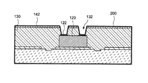
本発明の実施形態1に係る半導体パッケージの概要について、図1A及び図1Bを参照しながら詳細に説明する。図1Aは、本発明の一実施形態に係る半導体パッケージの断面模式図である。図1Bは、本発明の一実施形態に係るアライメントマーカと半導体装置との位置関係を示す平面模式図である。なお、図1Bでは、説明の便宜上半導体装置120よりも上層の、例えば配線140及びはんだボール160は省略して図示した。
<First embodiment>
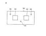
An outline of the semiconductor package according to the first embodiment of the present invention will be described in detail with reference to FIGS. 1A and 1B. FIG. 1A is a schematic sectional view of a semiconductor package according to an embodiment of the present invention. FIG. 1B is a schematic plan view illustrating a positional relationship between the alignment marker and the semiconductor device according to the embodiment of the present invention. In FIG. 1B, for example, the
[半導体パッケージ10の構造]
図1Aに示すように、半導体パッケージ10は、支持基材100、接着層110、半導体装置120、第1樹脂絶縁層130、配線140、第2樹脂絶縁層150、及びはんだボール160を有する。また、図1Bに示すように、支持基材100上において、半導体装置120の周囲にアライメントマーカ102が設けられている。図1Bでは、アライメントマーカ102は半導体装置120の対角に対応する位置に2つ設けられている。
[Structure of Semiconductor Package 10]
As shown in FIG. 1A, the
支持基材100には、支持基材100の一部が凹んだ形状のアライメントマーカ102(凹部)が設けられている。換言すると、半導体パッケージ10には平坦ではない支持基材100が用いられる。接着層110は支持基材100の表面に配置されており、アライメントマーカ102を露出するように接着層110の一部が開口されている。ここで、支持基材100の表面とは、支持基材100のアライメントマーカ102が設けられた面側を指す。なお、接着層110にはアライメントマーカ102よりも広い領域で開口された開口部112が設けられており、開口部112はアライメントマーカ102及びその周辺の支持基材100の表面を露出している。
The
ここで、アライメントマーカ102のサイズ(最も径が大きな箇所におけるサイズ)は0.05mm以上1.0mm以下の範囲で選択することができる。好ましくは、アライメントマーカ102のサイズは0.1mm以上0.3mm以下であるとよい。また、アライメントマーカ102と半導体装置120との距離は0.05mm以上0.5mm以下の範囲で選択することができる。ここで、アライメントマーカ102のサイズは、アライメントマーカの読み取り装置が認識可能なサイズであればよい。また、図1Bでは、アライメントマーカ102の形状が円形状である例を示したが、その他の形状であってもよい。また、アライメントマーカ102は数字や文字であってもよい。なお、アライメントマーカ102のサイズとは、1つのアライメントマーカ102において最も径が大きい箇所のサイズを意味する。また、アライメントマーカ102と半導体装置120との距離とは、両者の間隔のうち最も短い箇所の距離を意味する。
Here, the size of the alignment marker 102 (the size at the location with the largest diameter) can be selected in the range of 0.05 mm or more and 1.0 mm or less. Preferably, the size of
半導体装置120は、接着層110上に配置されている。半導体装置120の上部には、半導体装置120に含まれる電子回路に接続された外部端子122が設けられている。ここで、図1Aでは接着層110が単層である構造を例示したが、この構造に限定されず、接着層110は複数層であってもよい。また、図1Bでは1つの半導体装置120に対して2つのアライメントマーカ102が設けられた構成を例示したが、この構成に限定されない。例えば、アライメントマーカ102は1つの半導体装置120に対して少なくとも1つ以上設けられていればよい。また、アライメントマーカ102は1つの半導体装置120に対して3つ以上設けられていてもよい。
The
第1樹脂絶縁層130は半導体装置120を覆うように支持基材100上に配置されている。第1樹脂絶縁層130は開口部112及びアライメントマーカ102の凹部を埋めるように配置されている。換言すると、第1樹脂絶縁層130は開口部112の側壁に接している。同様に、第1樹脂絶縁層130はアライメントマーカ102の凹部の側壁に接している。また、第1樹脂絶縁層130には開口部132が設けられている。開口部132は外部端子122に達している。換言すると、開口部132は外部端子122を露出するように設けられている。
The first
ここで、図1Aでは、開口部112の側壁の形状が垂直であり、当該側壁と接着層110の表面とが直角をなしている構造を例示したが、この構造に限定されない。例えば、開口部112の側壁が接着層110の表面に対する垂線から傾斜したテーパ形状であってもよい。テーパ形状としては、開口部112の下方から上方に向かって開口径が大きくなる順テーパ形状であってもよく、逆に開口部112の下方から上方に向かって開口径が小さくなる逆テーパ形状であってもよい。また、開口部112の側壁と接着層110の表面との間が湾曲していてもよい。つまり、開口部112の側壁と接着層110の表面との角部が丸まった形状であってもよい。
Here, FIG. 1A illustrates a structure in which the shape of the side wall of the
配線140は第1導電層142及び第2導電層144を有する。第1導電層142は第1樹脂絶縁層130の上面に配置されている。第2導電層144は第1導電層142上及び開口部132内部に配置されており、外部端子122に接続されている。図1Aでは、第1導電層142は第1樹脂絶縁層130の上面のみに配置されており、開口部132の内部には全く配置されていない構造を例示したが、この構造に限定されない。例えば、第1導電層142の一部が開口部132内部に入り込んでいてもよい。第1導電層142及び第2導電層144の各々は、図1Aに示すように単層であってもよく、第1導電層142及び第2導電層の一方又は両方が複数層であってもよい。
The
第2樹脂絶縁層150は配線140を覆うように第1樹脂絶縁層130上に配置されている。また、第2樹脂絶縁層150には開口部152が設けられている。開口部152は配線140に達している。換言すると、開口部152は配線140を露出するように設けられている。
Second resin insulation layer (150) is arranged on first resin insulation layer (130) so as to cover wiring (140). An
はんだボール160は開口部152内部及び第2樹脂絶縁層150の上面に配置されており、配線140に接続されている。はんだボール160の上面は第2樹脂絶縁層150の上面から上方に突出している。はんだボール160の突出部は上に凸の湾曲形状を有している。はんだボール160の湾曲形状は断面視において円弧であってもよく、放物線であってもよい。
The
以上のように、実施形態1に係る半導体パッケージによると、第1樹脂絶縁層130がアライメントマーカ102の凹部の側壁に接していることで、接着層110と第1樹脂絶縁層130との密着性を向上させることができる。例えば、支持基材100にアライメントマーカ102を設けると、アライメントマーカ102が設けられた領域における接着層110による接着効果が弱くなってしまう。そのため、局所的に第1樹脂絶縁層130が支持基材100から剥離し、その剥離をきっかけとして第1樹脂絶縁層130が接着層110から剥離してしまうことがある。しかし、上記のように、第1樹脂絶縁層130がアライメントマーカ102の凹部の側壁に接していることで、局所的な第1樹脂絶縁層130の支持基材100からの剥離を抑制することができる。
As described above, according to the semiconductor package according to the first embodiment, since the first
[半導体パッケージ10の各部材の材質]
図1A及び図1Bに示す半導体パッケージ10に含まれる各部材(各層)の材料について詳細に説明する。
[Material of each member of semiconductor package 10]
The material of each member (each layer) included in the
支持基材100としては、金属基材を用いることができる。金属基材としては、ステンレス(SUS)基材、アルミニウム(Al)基材、チタン(Ti)基材、銅(Cu)等の金属材料を用いることができる。また、支持基材100として、金属基材の他にシリコン基板、炭化シリコン基板、化合物半導体基板などの半導体基材を用いることができる。なお、SUS基材は熱膨張率が低く、低価格であるため、支持基材100としてSUS基材を用いることが好ましい。
As the
接着層110としては、エポキシ系樹脂またはアクリル系樹脂を含む接着剤を用いることができる。
As the
半導体装置120としては、中央演算処理装置(Central Processing Unit;CPU)、メモリ、微小電気機械システム(Micro Electro Mechanical Systems;MEMS)、電力用半導体素子(パワーデバイス)などを用いることができる。
As the
第1樹脂絶縁層130及び第2樹脂絶縁層150としては、ポリイミド、エポキシ樹脂、ポリイミド樹脂、ベンゾシクロブテン樹脂、ポリアミド、フェノール樹脂、シリコーン樹脂、フッ素樹脂、液晶ポリマー、ポリアミドイミド、ポリベンゾオキサゾール、シアネート樹脂、アラミド、ポリオレフィン、ポリエステル、BTレジン、FR−4、FR−5、ポリアセタール、ポリブチレンテレフタレート、シンジオタクチック・ポリスチレン、ポリフェニレンサルファイド、ポリエーテルエーテルケトン、ポリエーテルニトリル、ポリカーボネート、ポリフェニレンエーテルポリサルホン、ポリエーテルスルホン、ポリアリレート、ポリエーテルイミドなどを用いることができる。なお、エポキシ系樹脂は電気特性および加工特性に優れているため、第1樹脂絶縁層130及び第2樹脂絶縁層150としてエポキシ系樹脂を用いることが好ましい。
As the first
ここで、本実施形態で用いられる第1樹脂絶縁層130にはフィラーが含まれている。フィラーとしては、ガラス、タルク、マイカ、シリカ、アルミナ等の無機フィラーが用いられてもよい。また、フィラーとしてフッ素樹脂フィラーなどの有機フィラーが用いられてもよい。ただし、第1樹脂絶縁層130が必ずフィラーを含む樹脂であることを限定するものではない。また、本実施形態では、第2樹脂絶縁層150はフィラーを含んでいないが、第2樹脂絶縁層150にフィラーが含まれていてもよい。
Here, the first
第1導電層142及び第2導電層144としては、銅(Cu)、金(Au)、銀(Ag)、白金(Pt)、ロジウム(Rh)、スズ(Sn)、アルミニウム(Al)、ニッケル(Ni)、パラジウム(Pd)、クロム(Cr)等の金属またはこれらを用いた合金などから選択することができる。第1導電層142と第2導電層144とは同じ材料を用いてもよく、異なる材料を用いてもよい。
As the first
はんだボール160としては、例えばSnに少量のAg、Cu、Ni、ビスマス(Bi)、又は亜鉛(Zn)を添加したSn合金で形成された球状の物体を用いることができる。また、はんだボール以外にも一般的な導電性粒子を使用することができる。例えば、導電性粒子として、粒子状の樹脂の周囲に導電性の膜が形成されたものを使用することができる。また、はんだボール以外に、はんだペーストを用いることができる。はんだペーストとしては、Sn、Ag、Cu、Ni、Bi、リン(P)、ゲルマニウム(Ge)、インジウム(In)、アンチモン(Sb)、コバルト(Co)、鉛(Pb)を用いることができる。
As the
[半導体パッケージ10の製造方法]
図2乃至図23を用いて、本発明の実施形態1に係る半導体パッケージ10の製造方法を説明する。図2乃至図23において、図1A及び図1Bに示す要素と同じ要素には同一の符号を付した。ここで、支持基材100としてSUS基材、第1樹脂絶縁層130としてエポキシ系樹脂、第1導電層142及び、第2導電層144としてCu、はんだボール160として上記Sn合金を使用して半導体パッケージを作製する製造方法について説明する。
[Method of Manufacturing Semiconductor Package 10]
The method for manufacturing the
図2は、本発明の一実施形態に係る半導体パッケージの製造方法において、支持基材にアライメントマーカを形成する工程を示す図である。アライメントマーカ102(凹部)は、フォトリソグラフィ及びエッチングによって形成される。アライメントマーカ102の位置及び平面形状は目的に応じて適宜決定することができる。アライメントマーカ102は、光学顕微鏡等で支持基材100を上面側から観察したときに、視認できる程度に段差が設けられていればよい。
FIG. 2 is a view showing a step of forming an alignment marker on a supporting base material in the method of manufacturing a semiconductor package according to one embodiment of the present invention. The alignment marker 102 (recess) is formed by photolithography and etching. The position and the planar shape of the
ここで、図2では、後の工程で半導体装置120が配置される領域に対して2つのアライメントマーカ102を形成する製造方法を例示したが、この製造方法に限定されない。例えば、アライメントマーカ102は1つの半導体装置120が配置される領域に対して少なくとも1つ以上設けられていればよい。また、アライメントマーカ102は1つの半導体装置120が配置される領域に対して3つ以上設けられていてもよい。
Here, FIG. 2 exemplifies a manufacturing method in which two
また、アライメントマーカ102の形成方法として、上記のフォトリソグラフィ及びエッチングによる形成以外の方法を用いることができる。例えば、支持基材100の表面からレーザ照射を行うことでアライメントマーカ102を形成してもよい。レーザ照射の一つとして、マスクを使用せずにレーザ光を走査することによって、支持基材100に直接描画を行うレーザ直描装置を用いることができる。または、アライメントマーカ102に対応する形状の金型を用いて支持基材100を形成することもできる。
In addition, as a method for forming the
図3は、本発明の一実施形態に係る半導体パッケージの製造方法において、支持基材に接着層を形成する工程を示す図である。アライメントマーカ102が形成された支持基材100の上面に接着層110を形成する。接着層110としてシート状の接着層を貼り付ける。なお、接着層110として接着層材料が溶解された溶媒を塗布法によって形成してもよい。図3では、アライメントマーカ102の凹部が空洞になっているが、アライメントマーカ102が形成された領域の接着層110は後の工程で除去されるので、この工程において接着層110がアライメントマーカ102の凹部に埋め込まれていてもよい。
FIG. 3 is a view showing a step of forming an adhesive layer on a supporting substrate in the method of manufacturing a semiconductor package according to one embodiment of the present invention. An
図4は、本発明の一実施形態に係る半導体パッケージの製造方法において、支持基材の裏面及び側面を粗化する工程を示す図である。ここでは、後の工程で無電解めっき法によって形成されるめっき層が剥離することを抑制する目的で、支持基材100の裏面及び側面を粗化(又は粗面化)する。支持基材100の粗化は、Cuを含む薬液(エッチャント)を用いることで行うことができる。図4において、粗化領域104を点線で示した。
FIG. 4 is a view showing a step of roughening the back surface and the side surface of the support base in the method of manufacturing a semiconductor package according to one embodiment of the present invention. Here, the back surface and side surfaces of the
支持基材100の粗化について、より詳細に説明する。支持基材100にSUS基材を用いる場合、SUS基材の表面は不動態化されている。ここで、上記のエッチャントに含まれるCuイオンはSUS基材中のFe、Cr、Niの少なくとも1つと置換されることでSUSがエッチングされる。しかし、SUSのエッチングは局所的に進行するため不均一にエッチングされ、エッチング後のSUS表面の凹凸が大きくなる。つまり、図4に示す状態でエッチャントに浸漬することで、SUS基材の裏面及び側面を同一処理で粗化することができる。
The roughening of the
なお、ここでは、接着層110を貼り付けた後にSUS基材の粗化を行う製造方法を例示したが、この製造方法に限定されない。例えば、接着層110を貼り付ける前、又はアライメントマーカ102を形成する前に粗化を行ってもよい。
Here, the manufacturing method in which the SUS base material is roughened after attaching the
図5は、本発明の一実施形態に係る半導体パッケージの製造方法において、接着層の一部を除去する工程を示す図である。アライメントマーカ102をより精度よく読み取るために、アライメントマーカ102の上方の接着層110を除去して開口部112を形成する。接着層110の除去は、例えばCO2レーザを用いたレーザ照射による昇華又はアブレーションによって行うことができる。又は、フォトリソグラフィ及びエッチングによって形成することもできる。開口部112はアライメントマーカ102を確実に露出するためにアライメントマーカ102よりも広い領域に形成される。つまり、開口部112は支持基材100の表面を露出する。換言すると、平面視において、開口部112はアライメントマーカ102を囲むように形成される。
FIG. 5 is a view showing a step of removing a part of the adhesive layer in the method of manufacturing a semiconductor package according to one embodiment of the present invention. In order to read the
図6は、本発明の一実施形態に係る半導体パッケージの製造方法において、支持基材上に半導体装置を配置する工程を示す図である。上記のようにして露出されたアライメントマーカ102に基づいて位置合わせを行い、上面(アライメントマーカ102が形成された面側)に外部端子122を有する半導体装置120を接着層110を介して支持基材100に配置する。アライメントマーカ102の読み取りは、例えば、光学顕微鏡、CCDカメラ、電子顕微鏡等の方法を行うことができる。この方法によって、高いアライメント精度で半導体装置120の実装を実現することができる。
FIG. 6 is a view showing a step of arranging a semiconductor device on a supporting base material in the method of manufacturing a semiconductor package according to one embodiment of the present invention. The alignment is performed based on the
図7は、本発明の一実施形態に係る半導体パッケージの製造方法において、樹脂絶縁層を形成する工程を示す図である。第1樹脂絶縁層130は、絶縁性のシート状フィルムの貼り付けによって形成される。具体的には、当該シート状フィルムを半導体装置120が実装された支持基材100に貼り付けた後に、加熱処理によってシート状フィルムを溶融させ、加圧処理によって溶融したシート状フィルムをアライメントマーカ102の凹部に埋め込む。この加熱処理および加圧処理によって上記シート状フィルムから、図7に示す第1樹脂絶縁層130を得る。第1樹脂絶縁層130は、開口部112及びアライメントマーカ102の凹部を埋めるように形成される。換言すると、第1樹脂絶縁層130は開口部112の側壁に接するように形成される。同様に、第1樹脂絶縁層130はアライメントマーカ102の凹部の側壁に接するように形成される。ここで、第1樹脂絶縁層130の膜厚は、第1樹脂絶縁層130が半導体装置120を覆うように設定される。つまり、第1樹脂絶縁層130の膜厚は半導体装置120の厚さよりも厚い。なお、第1樹脂絶縁層130は、半導体装置120、接着層110などによって形成された段差を緩和(平坦化)するため、平坦化膜と呼ばれることもある。
FIG. 7 is a view showing a step of forming a resin insulating layer in the method of manufacturing a semiconductor package according to one embodiment of the present invention. The first
ただし、第1樹脂絶縁層130は、半導体装置120及び外部端子122と配線140とが導通することを防ぐことができればよいため、半導体装置120及び外部端子122と配線140とのギャップが十分に確保できていればよい。つまり、第1樹脂絶縁層130が半導体装置120及び外部端子122の少なくとも上面及び側面に配置されていれば、半導体装置120が配置されていない領域における第1樹脂絶縁層130の膜厚は半導体装置120の厚さよりも薄くてもよい。また、図7の説明では、第1樹脂絶縁層130をスピンコート法で形成する製造方法を例示したが、この方法に限定されない。例えば、ディップ法、インクジェット法、蒸着法などの多様な方法で第1樹脂絶縁層130を形成することができる。
However, the first
図8は、本発明の一実施形態に係る半導体パッケージの製造方法において、樹脂絶縁層上に導電層を形成する工程を示す図である。第1樹脂絶縁層130の上面に導電性を有するシート状のフィルムを貼り付ける。ここで、この導電性フィルムは第1導電層142の一部である。ここでは、第1導電層142をフィルムの貼り付けによって形成する製造方法を例示したが、この方法に限定されない。例えば、第1導電層142は物理蒸着法(Physical Vapor Deposition;PVD法)によって形成されてもよい。PVD法としては、スパッタリング法、真空蒸着法、電子ビーム蒸着法、めっき法、及び分子線エピタキシー法などを用いることができる。また、導電性を有する樹脂材料が溶解された溶媒を塗布することで第1導電層142を形成してもよい。
FIG. 8 is a view showing a step of forming a conductive layer on a resin insulating layer in the method of manufacturing a semiconductor package according to one embodiment of the present invention. A sheet-like film having conductivity is attached to the upper surface of the first
図9は、本発明の一実施形態に係る半導体パッケージの製造方法において、導電層の表面を粗化する工程を示す図である。図9に示すように、第1樹脂絶縁層130上に形成された第1導電層142の表面を粗化する。第1導電層142表面の粗化は、塩化第二鉄薬液を用いたエッチングによって行うことができる。図9において、粗化領域146を点線で示した。
FIG. 9 is a view showing a step of roughening the surface of the conductive layer in the method of manufacturing a semiconductor package according to one embodiment of the present invention. As shown in FIG. 9, the surface of the first
図10は、本発明の一実施形態に係る半導体パッケージの製造方法において、樹脂絶縁層に開口部を形成する工程を示す図である。図10に示すように、外部端子122に対応する位置において、第1導電層142表面の粗化領域146に対してレーザを照射することによって外部端子122を露出する開口部132を形成する。開口部132の形成は、第1導電層142及び第1樹脂絶縁層130に対して一括で行うことができる。開口部132を形成するためのレーザとして、CO2レーザを用いることができる。CO2レーザは、開口部132のサイズに合わせてスポット径およびエネルギー量が調整され、複数回パルス照射される。ここで、第1導電層142の表面に粗化領域146が形成されていることで、照射されたレーザ光のエネルギーを効率よく第1導電層142に吸収させることができる。レーザ光は外部端子122の内側に照射される。つまり、レーザ光は外部端子122のパターンを外れないように照射される。ただし、半導体装置120の一部を加工したい場合は、意図的にレーザ光の一部が外部端子122の外側にはみ出すように照射してもよい。
FIG. 10 is a view showing a step of forming an opening in the resin insulating layer in the method of manufacturing a semiconductor package according to one embodiment of the present invention. As shown in FIG. 10, an
なお、図10では、開口された第1導電層142の側壁と第1樹脂絶縁層130の側壁とが連続している構造を例示したが、この構造に限定されない。例えば、レーザ照射によって開口する場合、第1導電層142に比べて第1樹脂絶縁層130の方が支持基材100の平面方向(開口径が広がる方向)に大きく後退し、第1導電層142の端部が第1樹脂絶縁層130の端部よりも開口部132の内側方向に突出した構造になってもよい。換言すると、開口部132は第1導電層142が突出したひさし形状になってもよい。また換言すると、開口部132が形成された時点において、第1導電層142の一部の下面が開口部132の内部に露出されてもよい。その際に、開口部132の内側方向に突出した第1導電層142が開口部132の内部において外部端子122の方向に屈曲した形状になってもよい。
Although FIG. 10 illustrates a structure in which the opened sidewall of the first
図11は、本発明の一実施形態に係る半導体パッケージの製造方法において、導電層の表面の粗化された領域を除去し、開口底部の残渣を除去する工程を示す図である。まず、開口部132を形成した後に第1導電層142表面の粗化領域146を除去する。粗化領域146の除去は、酸処理によって行うことができる。粗化領域146の除去に続いて、開口部132の底部の残渣(スミア)を除去する。ここで、残渣の除去(デスミア)は2段階の工程で行われる。
FIG. 11 is a view showing a step of removing a roughened region on the surface of the conductive layer and removing residues at the bottom of the opening in the method of manufacturing a semiconductor package according to one embodiment of the present invention. First, after forming the
ここで、開口部132の底部の残渣を除去する方法について詳細に説明する。まず、開口部132の底部に対してプラズマ処理を行う。プラズマ処理としては、フッ素(CF4)ガス及び酸素(O2)ガスを含むプラズマ処理を用いることができる。プラズマ処理は、主に開口部132の形成時に除去しきれなかった第1樹脂絶縁層130を除去する。このとき、開口部132の形成時に発生した第1樹脂絶縁層130の変質層を除去することもできる。例えば、開口部132をレーザ照射で形成した場合、レーザのエネルギーによって変質した第1樹脂絶縁層130が開口部132の底部に残ることがある。ここで、上記のようにプラズマ処理を行うことで、上記の変質層を効率良く除去することができる。
Here, a method for removing the residue at the bottom of the
上記のプラズマ処理に続いて、薬液処理を行う。薬液処理としては、少なくとも過マンガン酸ナトリウム又は過マンガン酸カリウムを用いることができる。薬液処理は、上記のプラズマ処理によって除去しきれなかった残渣を除去することができる。例えば、第1樹脂絶縁層130に含まれ、上記のプラズマ処理では除去することができなかったフィラーを除去することができる。なお、過マンガン酸ナトリウム又は過マンガン酸カリウムは、残渣をエッチングするための役割を有するエッチング液である。ここで、上記のエッチング液による処理の前に第1樹脂絶縁層130を膨潤させる膨潤液を用いることもできる。また、上記のエッチング液による処理の後にエッチング液を中和する中和液を用いることもできる。
Subsequent to the plasma treatment, a chemical treatment is performed. As the chemical treatment, at least sodium permanganate or potassium permanganate can be used. The chemical treatment can remove residues that could not be completely removed by the above plasma treatment. For example, a filler included in the first
膨潤液を用いることで、樹脂環が拡がるため液の濡れ性が高くなる。これによって、エッチングされない領域の発生を抑制することができる。中和液を用いることで、エッチング液を効率よく除去することができるため、意図しないエッチングの進行を抑制することができる。例えば、エッチング液にアルカリ性の薬液を用いた場合、アルカリ性の薬液は水洗では除去しにくいため、意図しないエッチングが進んでしまうことがある。このような場合であっても、エッチング後に中和液を用いれば、意図しないエッチングの進行を抑制することができる。 By using the swelling liquid, the resin ring expands, and the wettability of the liquid increases. This can suppress the generation of a region that is not etched. By using the neutralizing solution, the etching solution can be efficiently removed, so that unintended progress of etching can be suppressed. For example, when an alkaline chemical is used as an etchant, the alkaline chemical is difficult to remove by washing with water, so that unintended etching may proceed. Even in such a case, if a neutralizing solution is used after the etching, unintended progress of the etching can be suppressed.
ここで、膨潤液としては、ジエチレングリコール モノブチルエーテル、エチレングリコールなどの有機溶剤を用いることができる。また、中和液としては、硫酸ヒドロキシルアミンなどの硫酸系の薬液を用いることができる。 Here, as the swelling liquid, an organic solvent such as diethylene glycol monobutyl ether and ethylene glycol can be used. As the neutralizing solution, a sulfuric acid-based chemical such as hydroxylamine sulfate can be used.
例えば第1樹脂絶縁層130に無機材料のフィラーを用いた場合、フィラーはプラズマ処理で除去することができず、残渣となる場合がある。このような場合であっても、プラズマ処理の後に薬液処理を行うことで、フィラーに起因する残渣を除去することができる。
For example, when a filler made of an inorganic material is used for the first
図12は、本発明の一実施形態に係る半導体パッケージの製造方法において、無電解めっき法によって導電層を形成する工程を示す図である。無電解めっき法によって、上記のデスミア工程後に露出された外部端子122に接続されるめっき層200(導電体)を形成する。無電解めっき法は、パラジウム(Pd)コロイドを樹脂上に吸着させてCuを含む薬液中に浸漬させ、PdとCuを置換することでCuを析出させる方法を用いることができる。ここで、粗化領域146を除去してから無電解めっき法によってめっき層200を形成することで、第1導電層142に対するめっき層200の密着性を向上させることができる。
FIG. 12 is a view showing a step of forming a conductive layer by an electroless plating method in the method of manufacturing a semiconductor package according to one embodiment of the present invention. A plating layer 200 (conductor) connected to the
図13は、本発明の一実施形態に係る半導体パッケージの製造方法において、感光性フォトレジストを形成する工程を示す図である。図13に示すように、めっき層200上に感光性のフォトレジスト210を形成する。フォトレジストはスピンコート法などの塗布法によって形成される。フォトレジスト形成前に、めっき層200とフォトレジスト210との密着性を向上させる処理(HMDS処理などの疎水化表面処理)をおこなってもよい。フォトレジスト210は、感光された領域が現像液に対してエッチングされにくくなるネガ型を用いることもでき、逆に感光された領域が現像液によってエッチングされるポジ型を用いることもできる。
FIG. 13 is a view showing a step of forming a photosensitive photoresist in the method of manufacturing a semiconductor package according to one embodiment of the present invention. As shown in FIG. 13, a
図14は、本発明の一実施形態に係る半導体パッケージの製造方法において、フォトリソグラフィによって感光性フォトレジストの一部を除去する工程を示す図である。塗布されたフォトレジスト210に対して露光及び現像を行うことで、図1に示す配線140を形成する領域のフォトレジスト210を除去して、図14に示すようなレジストパターン220を形成する。なお、レジストパターン220を形成する露光を行う際に、支持基材100に形成されたアライメントマーカ102を用いて位置合わせを行う。
FIG. 14 is a view showing a step of removing a part of the photosensitive photoresist by photolithography in the method of manufacturing a semiconductor package according to one embodiment of the present invention. By exposing and developing the applied
図15は、本発明の一実施形態に係る半導体パッケージの製造方法において、電解めっき法によって導電層を形成する工程を示す図である。レジストパターン220を形成後、無電解めっき法によって形成されためっき層200に通電して電解めっき法を行い、レジストパターン220から露出しているめっき層200をさらに成長させて厚膜化して第2導電層144を形成する。ここで、レジストパターン220下の第1導電層142及びめっき層200は、全面をエッチングすることで除去するため、厚膜化された第2導電層144も膜減りする。したがって、上記の膜減り量を考慮して厚膜化する第2導電層144の量を調整する。
FIG. 15 is a view showing a step of forming a conductive layer by an electrolytic plating method in the method of manufacturing a semiconductor package according to one embodiment of the present invention. After the formation of the resist
図16は、本発明の一実施形態に係る半導体パッケージの製造方法において、感光性フォトレジストを除去する工程を示す図である。図16に示すように、めっき層200を厚膜化して第2導電層144を形成した後に、レジストパターン220を構成するフォトレジストを有機溶媒により除去する。なお、フォトレジストの除去には、有機溶媒を用いる代わりに、酸素プラズマによるアッシングを用いることもできる。フォトレジストを除去することで、第2導電層144が形成された厚膜領域230及びめっき層200のみが形成された薄膜領域240を得ることができる。なお、厚膜領域230において、第2導電層144はめっき層200上に電解めっき法によって厚膜化されためっき層が形成されているため、厳密には2層で形成されているが、ここではその2層を区別せずに図示した。
FIG. 16 is a view showing a step of removing a photosensitive photoresist in a method of manufacturing a semiconductor package according to an embodiment of the present invention. As shown in FIG. 16, after forming the second
図17は、本発明の一実施形態に係る半導体パッケージの製造方法において、導電層の一部を除去して配線を形成する工程を示す図である。図17に示すように、レジストパターン220によって覆われ、厚膜化されなかった領域のめっき層200及び第1導電層142を除去(エッチング)することで、各々の配線140を電気的に分離する。めっき層200及び第1導電層142のエッチングによって、厚膜領域230の第2導電層144の表面もエッチングされて薄膜化するため、この薄膜化の影響を考慮して第2導電層144の膜厚を設定することが好ましい。この工程におけるエッチングとしては、ウェットエッチングやドライエッチングを使用することができる。なお、図17では、配線140を1層形成する製造方法を例示したが、この方法に限定されず、配線140の上方に絶縁層及び導電層を積層させ、複数の配線層が積層された多層配線を形成してもよい。その際に、配線層を形成する度に新たにアライメントマーカを形成し、上層の配線層形成の際の位置合わせに利用してもよい。
FIG. 17 is a view showing a step of forming a wiring by removing a part of the conductive layer in the method of manufacturing a semiconductor package according to one embodiment of the present invention. As shown in FIG. 17, by removing (etching) the
図18は、本発明の一実施形態に係る半導体パッケージの製造方法において、配線を覆う樹脂絶縁層を形成する工程を示す図である。第2樹脂絶縁層150は第1樹脂絶縁層130と同様に、絶縁性のシート状フィルムを貼り付け、加熱・加圧処理を行うことで形成する。ここで、第2樹脂絶縁層150の膜厚は、第2樹脂絶縁層150が配線140を覆うように設定される。つまり、第2樹脂絶縁層150の膜厚は配線140の厚さよりも厚い。なお、第2樹脂絶縁層150は、配線140などによって形成された段差を緩和(平坦化)するため、平坦化膜と呼ばれることもある。
FIG. 18 is a view showing a step of forming a resin insulating layer covering the wiring in the method of manufacturing a semiconductor package according to one embodiment of the present invention. Similarly to the first
ただし、第2樹脂絶縁層150は、配線140とはんだボール160とが導通することを防ぐことができればよいため、配線140とはんだボール160とのギャップが十分に確保できていればよい。つまり、第2樹脂絶縁層150が配線140の少なくとも上面及び側面に配置されていれば、配線140が配置されていない領域における第2樹脂絶縁層150の膜厚は配線140の厚さよりも薄くてもよい。また、図18の説明では、第2樹脂絶縁層150をスピンコート法で形成する製造方法を例示したが、この方法に限定されない。例えば、ディップ法、インクジェット法、蒸着法などの多様な方法で第2樹脂絶縁層150を形成することができる。
However, since the second
図19は、本発明の一実施形態に係る半導体パッケージの製造方法において、樹脂絶縁層に配線を露出する開口部を形成する工程を示す図である。図19に示すように、第2樹脂絶縁層150に配線140を露出する開口部152を形成する。開口部152はフォトリソグラフィ及びエッチングによって形成してもよく、第2樹脂絶縁層150として感光性樹脂を用いた場合は露光及び現像によって形成してもよい。ここで、第1樹脂絶縁層130の開口部132に対して行われたデスミア処理を開口部152に対して行ってもよい。ここで、配線140と同じ工程で形成したアライメントマーカに基づいて位置合わせすることで、開口部152を形成することができる。
FIG. 19 is a view showing a step of forming an opening exposing a wiring in a resin insulating layer in the method of manufacturing a semiconductor package according to one embodiment of the present invention. As shown in FIG. 19, an
図20は、本発明の一実施形態に係る半導体パッケージの製造方法において、露出された配線に対応する位置にはんだボールを配置する工程を示す図である。図20に示すように、開口部152に対してはんだボール160を配置する。なお、図20では、1つの開口部152に対して1つのはんだボール160が配置された製造方法を例示したが、この方法に限定されず、1つの開口部152に複数のはんだボール160が配置されてもよい。また、図20では、はんだボール160を開口部152に配置した段階で、はんだボール160が配線140に接触している製造方法を例示したが、この方法に限定されず、図20に示す段階においてははんだボール160が配線140に接触していなくてもよい。ここで、配線140と同じ工程で形成したアライメントマーカに基づいて位置合わせすることで、はんだボール160を配置することができる。
FIG. 20 is a view showing a step of arranging solder balls at positions corresponding to exposed wiring in the method of manufacturing a semiconductor package according to one embodiment of the present invention. As shown in FIG. 20,
図21は、本発明の一実施形態に係る半導体パッケージの製造方法において、はんだボールをリフロ―する工程を示す図である。図20に示す状態で熱処理を行うことで、はんだボール160をリフロ―させる。リフロ―とは固体の対象物の少なくとも一部を液状化させて流動性を持たせることで、対象物を凹部の内部に流し込むことである。はんだボール160をリフロ―することで、開口部152の内部で露出された配線140の上面の全域においてはんだボール160と配線140とを接触させることができる。
FIG. 21 is a view showing a step of reflowing a solder ball in the method of manufacturing a semiconductor package according to one embodiment of the present invention. By performing the heat treatment in the state shown in FIG. 20, the
図22は、本発明の一実施形態に係る半導体パッケージの製造方法において、樹脂絶縁層に支持基材に達する溝を形成する工程を示す図である。ここでは、ダイシングブレード(例えば、ダイヤモンド製の円形回転刃)を用いて接着層110、第1樹脂絶縁層130、及び第2樹脂絶縁層150に切り込み250を入れる。切り込み250の形成は、ダイシングブレードを高速回転させ、純水で冷却・切削屑の洗い流しを行いながら切断することで行われる。切り込み250は接着層110、第1樹脂絶縁層130、及び第2樹脂絶縁層150に形成されるが、支持基材100に達するようにダイシングし、支持基材100の上面付近に凹部が形成されてもよい。逆に、接着層110の一部、又は接着層110及び第1樹脂絶縁層130の一部を残すようにダイシングしてもよい。
FIG. 22 is a view showing a step of forming a groove reaching the support base in the resin insulating layer in the method of manufacturing a semiconductor package according to one embodiment of the present invention. Here, a
図23は、本発明の一実施形態に係る半導体パッケージの製造方法において、支持基材を切断して半導体パッケージを個片化する工程を示す図である。図23に示すように、支持基材100の裏面側(半導体装置120が配置された側とは逆側)からレーザ照射することで半導体パッケージを個片化する。支持基材100に照射するレーザとしては、CO2レーザを用いることができる。ここで、支持基材100のアライメントマーカ102に基づいて位置合わせすることで、レーザ照射を行うことができる。レーザは切り込み250よりも狭い領域に対して照射される。
FIG. 23 is a view showing a step of cutting the supporting base material to singulate the semiconductor package in the method of manufacturing a semiconductor package according to one embodiment of the present invention. As shown in FIG. 23, the semiconductor package is singulated by irradiating a laser from the back side of the supporting base material 100 (the side opposite to the side on which the
なお、ここでは支持基材100の裏面側からレーザ照射をおこなう製造方法を例示したが、この方法に限定されず、切り込み250を通過させて支持基材100の表面側からレーザ照射を行ってもよい。また、レーザを照射する領域が切り込み250が形成された領域よりも狭い製造方法を例示したが、この方法に限定されない。例えば、レーザを切り込み250が形成された領域と同じ領域に照射してもよく、それよりも広い領域に照射してもよい。
Here, the manufacturing method in which the laser irradiation is performed from the back surface side of the
ここで、支持基材100に金属基材を用いた場合、接着層110、第1樹脂絶縁層130、第2樹脂絶縁層150、及び支持基材100を一括で加工しようとすると、ダイシングブレードの消耗が大きくなり、ダイシングブレードの使用寿命が短くなってしまう。また、金属基材をダイシングブレードで機械的に加工すると、加工端において角の形状が鋭利な「ばり」が発生してしまい、ハンドリングの際に作業者がけがをする危険性がある。しかし、支持基材100をレーザ加工することで、ダイシングブレードの消耗を避けることができ、支持基材100の加工端の形状を滑らかにすることができる。したがって、特に支持基材100として金属基材を用いた場合、上記のように支持基材100上の構造物をダイシングブレードで加工し、支持基材100をレーザで加工することが好ましい。
Here, when a metal base is used for the
以上のように、実施形態1に係る半導体パッケージの製造方法によると、半導体装置120を支持基材100に配置する前に、支持基材100にアライメントマーカを形成することで、半導体装置120の配置におけるアライメント精度を向上させることができる。
As described above, according to the method for manufacturing a semiconductor package according to the first embodiment, the alignment marker is formed on the
〈実施形態2〉
本発明の実施形態2に係る半導体パッケージの製造方法において、半導体装置を配置する際のアライメント方法について、図24を参照しながら詳細に説明する。図24は、本発明の一実施形態に係るアライメントマーカと半導体装置との位置関係を示す平面模式図である。図24では、説明の便宜上、支持基材(300)、半導体装置(320、322)、及びアライメントマーカ(302、304、306)のみを表示したが、図1Aと同様の構造とすることができる。
<Embodiment 2>
In the method of manufacturing a semiconductor package according to the second embodiment of the present invention, an alignment method for arranging a semiconductor device will be described in detail with reference to FIG. FIG. 24 is a schematic plan view illustrating a positional relationship between an alignment marker and a semiconductor device according to an embodiment of the present invention. In FIG. 24, for convenience of explanation, only the support base material (300), the semiconductor devices (320, 322), and the alignment markers (302, 304, 306) are displayed, but the structure may be the same as that in FIG. 1A. .
[半導体パッケージ20の構造]
図24に示すように、半導体パッケージ20は、支持基材300上において、第1半導体装置320及び第2半導体装置322の周囲に第1アライメントマーカ302(第1凹部)、第2アライメントマーカ304(第2凹部)、及び第3アライメントマーカ306(第3凹部)が設けられている。第1アライメントマーカ302及び第2アライメントマーカ304は第1半導体装置320の対角に対応する位置に設けられており、第2アライメントマーカ304及び第3アライメントマーカ306は第2半導体装置322の対角に対応する位置に設けられている。換言すると、第1半導体装置320と第2半導体装置322との間に第2アライメントマーカ304が設けられている。
[Structure of Semiconductor Package 20]
As shown in FIG. 24, the
[半導体パッケージ20の製造工程におけるアライメント方法]
図24を用いて、第1半導体装置320及び第2半導体装置322のアライメント方法について詳細に説明する。まず、図2に示した方法と同様の方法で支持基材300に第1アライメントマーカ302、第2アライメントマーカ304、及び第3アライメントマーカ306を形成する。次に、図6に示した方法と同様の方法で第1アライメントマーカ302及び第2アライメントマーカ304に基づいて位置合わせを行って第1半導体装置320を配置し、第2アライメントマーカ304及び第3アライメントマーカ306に基づいて位置合わせを行って第2半導体装置322を配置する。そして、第1半導体装置320及び第2半導体装置322を覆う第1樹脂絶縁層130を形成する。上記以外の製造工程は、図2〜図23と同様の方法で製造することができる。
[Alignment Method in Manufacturing Process of Semiconductor Package 20]
A method for aligning the
上記のように、半導体パッケージ20の製造工程では、第1半導体装置320のアライメントマーカと第2半導体装置322のアライメントマーカとを共有させる。換言すると、半導体パッケージ20の製造工程における半導体装置(320、322)を配置する際に用いられるアライメントマーカの数は、実施形態1の半導体パッケージ10の製造工程における半導体装置120を配置する際に用いられるアライメントマーカの数よりも少ない。また換言すると、実施形態1の半導体パッケージ10の製造方法では、1つの半導体装置120を配置する際に2つのアライメントマーカ102を用いていたが、半導体パッケージ20の製造方法では、2つの半導体装置(320、322)を配置する際に3つのアライメントマーカ(302、304、306)を用いる。つまり、半導体パッケージ20の製造方法では、1つの半導体装置を配置する際に1.5のアライメントマーカを用いて行うことができる。
As described above, in the manufacturing process of the
半導体パッケージ20の製造工程において、各々の半導体パッケージ20を個片化する際に、第2アライメントマーカ304が第1半導体装置320側又は第2半導体装置322側のいずれかに含まれるように支持基材300が分断されてもよい。又は、各々の半導体パッケージ20を個片化する際に、第2アライメントマーカ304が2つに分断され、第1半導体装置320側に第2アライメントマーカ304の一部が含まれ、第2半導体装置322側に第2アライメントマーカ304の残りの部分が含まれるように支持基材300が分断されてもよい。又は、各々の半導体パッケージ20の個片化の際に、第2アライメントマーカ304が消失してもよい。つまり、個片化された半導体パッケージ20に含まれるアライメントマーカの数が2つ未満であってもよい。
In the manufacturing process of the
以上のように、実施形態2に係る半導体パッケージ20によると、半導体装置を配置するためのアライメントマーカの数を低減することができる。したがって、アライメントマーカを個別に形成する製造方法の場合に、アライメントを形成する工程を短縮することができる。上記の構成は、アライメントマーカを配置する領域が十分に確保することが難しい場合にも有効である。
As described above, according to the
〈実施形態3〉
本発明の実施形態3に係る半導体パッケージの製造方法において、半導体装置を配置する際のアライメント方法について、図25を参照しながら詳細に説明する。図25は、本発明の一実施形態に係るアライメントマーカと半導体装置との位置関係を示す平面模式図である。図25では、説明の便宜上、支持基材(400)、半導体装置(420、422、424、426)、及びアライメントマーカ(401、403、405、407、409)のみを表示したが、図1Aと同様の構造とすることができる。
<Embodiment 3>
In the method of manufacturing a semiconductor package according to the third embodiment of the present invention, an alignment method for arranging a semiconductor device will be described in detail with reference to FIG. FIG. 25 is a schematic plan view illustrating a positional relationship between an alignment marker and a semiconductor device according to an embodiment of the present invention. In FIG. 25, only the support substrate (400), the semiconductor devices (420, 422, 424, 426), and the alignment markers (401, 403, 405, 407, 409) are displayed for convenience of explanation. A similar structure can be used.
[半導体パッケージ30の構造]
図25に示すように、半導体パッケージ30は、支持基材400上において、第1半導体装置420、第2半導体装置422、第3半導体装置424、及び第4半導体装置426の周囲に第1アライメントマーカ401、第2アライメントマーカ403、第3アライメントマーカ405、第4アライメントマーカ407、及び第5アライメントマーカ409が設けられている。
[Structure of Semiconductor Package 30]
As shown in FIG. 25, the
第1アライメントマーカ401及び第3アライメントマーカ405は第1半導体装置420の対角に対応する位置に設けられている。第2アライメントマーカ403及び第3アライメントマーカ405は第2半導体装置422の対角に対応する位置に設けられている。第3アライメントマーカ405及び第4アライメントマーカ407は第3半導体装置424の対角に対応する位置に設けられている。第3アライメントマーカ405及び第5アライメントマーカ409は第4半導体装置426の対角に対応する位置に設けられている。換言すると、第1半導体装置420と、第2半導体装置422と、第3半導体装置424と、第4半導体装置426との間に第3アライメントマーカ405が設けられている。
The
[半導体パッケージ30の製造工程におけるアライメント方法]
図25を用いて、第1半導体装置420、第2半導体装置422、第3半導体装置424、及び第4半導体装置426のアライメント方法について詳細に説明する。まず、図2に示した方法と同様の方法で支持基材400に第1アライメントマーカ401、第2アライメントマーカ403、第3アライメントマーカ405、第4アライメントマーカ407、及び第5アライメントマーカ409を形成する。次に、図6に示した方法と同様の方法で第1アライメントマーカ401及び第3アライメントマーカ405に基づいて位置合わせを行って第1半導体装置420を配置し、第2アライメントマーカ403及び第3アライメントマーカ405に基づいて位置合わせを行って第2半導体装置422を配置し、第3アライメントマーカ405及び第4アライメントマーカ407に基づいて位置合わせを行って第3半導体装置424を配置し、第3アライメントマーカ405及び第5アライメントマーカ409に基づいて位置合わせを行って第4半導体装置426を配置する。そして、第1半導体装置420、第2半導体装置422、第3半導体装置424、及び第4半導体装置426を覆う第1樹脂絶縁層130を形成する。上記以外の製造工程は、図2〜図23と同様の方法で製造することができる。
[Alignment Method in Manufacturing Process of Semiconductor Package 30]
A method for aligning the
上記のように、半導体パッケージ30の製造工程では、第1半導体装置420のアライメントマーカ、第2半導体装置422のアライメントマーカ、第3半導体装置424のアライメントマーカ、及び第4半導体装置426のアライメントマーカを共有させる。換言すると、半導体パッケージ30の製造工程における半導体装置(420、422、424、426)を配置する際に用いられるアライメントマーカの数は、実施形態1の半導体パッケージ10の製造工程における半導体装置120を配置する際に用いられるアライメントマーカの数よりも少ない。また換言すると、実施形態1の半導体パッケージ10の製造方法では、1つの半導体装置120を配置する際に2つのアライメントマーカ102を用いていたが、半導体パッケージ30の製造方法では、4つの半導体装置(420、422、424、426)を配置する際に5つのアライメントマーカ(401、403、405、407、409)を用いる。つまり、半導体パッケージ30の製造方法では、1つの半導体装置を配置する際に1.25のアライメントマーカを用いて行うことができる。
As described above, in the manufacturing process of the
半導体パッケージ30の製造工程において、各々の半導体パッケージ30を個片化する際に、第3アライメントマーカ405が第1半導体装置420側、第2半導体装置422側、第3半導体装置424側、又は第4半導体装置426側のいずれかに含まれるように支持基材400が分断されてもよい。又は、各々の半導体パッケージ30を個片化する際に、第3アライメントマーカ405を2〜4つに分断してもよい。又は、各々の半導体パッケージ30の個片化の際に、第3アライメントマーカ405が消失してもよい。つまり、個片化された半導体パッケージ30に含まれるアライメントマーカの数が2つ未満であってもよい。
In the manufacturing process of the
以上のように、実施形態3に係る半導体パッケージ30によると、半導体装置を配置するためのアライメントマーカの数を低減することができる。したがって、アライメントマーカを個別に形成する製造方法の場合に、アライメントを形成する工程を短縮することができる。
As described above, according to the
なお、本発明は上記実施の形態に限られたものではなく、要旨を逸脱しない範囲で適宜変更することが可能である。 Note that the present invention is not limited to the above-described embodiment, and can be appropriately changed without departing from the gist.
10、20、30:半導体パッケージ
100、300、400:支持基材
102、302、304、306、401、403、405、407、409:アライメントマーカ
104:粗化領域
110:接着層
112:開口部
120、320、322、420、422、424、426:半導体装置
122:外部端子
130:第1樹脂絶縁層
132、152:開口部
140:配線
142:第1導電層
144:第2導電層
146:粗化領域
150:第2樹脂絶縁層
160:はんだボール
200:めっき層
210:フォトレジスト
220:レジストパターン
230:厚膜領域
240:薄膜領域
250:切り込み
10, 20, 30:
Claims (11)
前記基材の前記少なくとも1つの凹部が設けられた面側に配置された半導体装置と、
前記半導体装置を覆う樹脂絶縁層と、
前記基材と前記半導体装置との間に配置された接着層と、
を有し、
前記接着層は、前記少なくとも1つの凹部を露出する開口部を有し、
前記開口部の端部は、平面視で前記少なくとも1つの凹部に隣接し、
前記樹脂絶縁層は、前記開口部を規定する前記接着層の側壁に接していることを特徴とする半導体パッケージ。 A substrate provided with at least one recess,
A semiconductor device disposed on a surface side of the base member on which the at least one concave portion is provided;
A resin insulating layer covering the semiconductor device;
An adhesive layer disposed between the substrate and the semiconductor device,
Have a,
The adhesive layer has an opening exposing the at least one recess,
An end of the opening is adjacent to the at least one recess in plan view,
The semiconductor package , wherein the resin insulating layer is in contact with a side wall of the adhesive layer that defines the opening .
前記樹脂絶縁層は、前記半導体装置の上方に設けられ、
前記導電層は、前記半導体装置及び前記樹脂絶縁層の上方に設けられ、
前記導電層は、前記樹脂絶縁層に設けられた開口を通って前記半導体装置に接続されていることを特徴とする請求項1に記載の半導体パッケージ。 Electrically connected to the conductive layer further have the said semiconductor device,
The resin insulating layer is provided above the semiconductor device,
The conductive layer is provided above the semiconductor device and the resin insulating layer,
The semiconductor package according to claim 1, wherein the conductive layer is connected to the semiconductor device through an opening provided in the resin insulating layer .
前記開口部には、導電性材料を含んだ、前記半導体装置に接続された構造体が設けられていないことを特徴とする請求項1に記載の半導体パッケージ。 The end of the opening continuously surrounds the at least one recess;
2. The semiconductor package according to claim 1 , wherein the opening is not provided with a structure including a conductive material and connected to the semiconductor device .
前記開口部には、導電性材料を含んだ、前記半導体装置に接続された構造体が設けられていないことを特徴とする請求項1に記載の半導体パッケージ。 Two or more recesses are provided, and are provided at positions corresponding to diagonals of the semiconductor device, respectively.
2. The semiconductor package according to claim 1, wherein the opening is not provided with a structure including a conductive material and connected to the semiconductor device .
前記第1凹部が形成された前記基材の表面に接着層を形成し、
前記接着層は、前記第1凹部を露出する第1開口部を含み、
前記第1開口部の端部は、平面視で前記第1凹部を囲み、
前記第1凹部に基づいて位置合わせして、半導体装置を前記接着層の表面に配置し、
前記半導体装置を覆う樹脂絶縁層を形成し、
前記樹脂絶縁層は、前記第1開口部を規定する前記接着層の側壁に接していることを特徴とする半導体パッケージの製造方法。 Forming a first recess in the substrate,
Forming an adhesive layer on the surface of the substrate on which the first recess is formed;
The adhesive layer includes a first opening exposing the first recess,
The end of the first opening surrounds the first recess in plan view,
Positioning the semiconductor device on the surface of the adhesive layer , based on the first recess,
Forming a resin insulating layer covering the semiconductor device ,
The method of manufacturing a semiconductor package , wherein the resin insulating layer is in contact with a side wall of the adhesive layer that defines the first opening .
前記外部端子に接続されるように、前記樹脂絶縁層の上及び前記樹脂絶縁層の前記開口の中に導電層をさらに形成することを特徴とする請求項5に記載の半導体パッケージの製造方法。 An opening exposing an external terminal of the semiconductor device is further formed in the resin insulating layer;
6. The method according to claim 5, further comprising forming a conductive layer on the resin insulating layer and in the opening of the resin insulating layer so as to be connected to the external terminal .
前記接着層を形成することは、前記第2凹部を露出する第2開口部を前記接着層に形成することを含み、
前記位置合わせは、前記第1凹部及び前記第2凹部に基づいて行われることを特徴とする請求項5に記載の半導体パッケージの製造方法。 A second recess is further formed in the base material,
Forming the adhesive layer includes forming a second opening exposing the second recess in the adhesive layer,
The method according to claim 5, wherein the positioning is performed based on the first concave portion and the second concave portion .
前記第1凹部、前記第2凹部、及び前記第3凹部が形成された前記基材の表面に接着層を形成し、
前記接着層は、
前記第1凹部を露出する第1開口部を含み、
前記第2凹部を露出する第2開口部を含み、
前記第3凹部を露出する第3開口部を含み、
前記第1開口部の端部は、平面視で前記第1凹部を囲み、
前記第1凹部は、前記基材の前記表面の一部が前記端部と前記第1凹部との間に位置するように、前記端部の内側に配置され、
前記第1凹部及び前記第2凹部に基づいて位置合わせして、第1半導体装置を前記接着層上に配置し、
前記第2凹部及び前記第3凹部に基づいて位置合わせして、第2半導体装置を前記接着層上に配置し、
前記第1半導体装置及び前記第2半導体装置を覆う樹脂絶縁層を形成し、
前記樹脂絶縁層は、前記第1開口部の側壁、前記第2開口部の側壁、及び前記第3開口部の側壁に接していることを特徴とする半導体パッケージの製造方法。 Forming a first recess, a second recess, and a third recess in the base material;
Forming an adhesive layer on the surface of the substrate on which the first recess, the second recess, and the third recess are formed;
The adhesive layer,
A first opening exposing the first recess;
A second opening exposing the second recess;
A third opening exposing the third recess;
The end of the first opening surrounds the first recess in plan view,
The first recess is disposed inside the end so that a part of the surface of the base material is located between the end and the first recess,
Positioning the first semiconductor device on the adhesive layer based on the first concave portion and the second concave portion;
Positioning the second semiconductor device on the adhesive layer based on the second concave portion and the third concave portion;
Forming a resin insulating layer covering the first semiconductor device and the second semiconductor device ;
The method of manufacturing a semiconductor package, wherein the resin insulating layer is in contact with a side wall of the first opening, a side wall of the second opening, and a side wall of the third opening .
前記外部端子に接続されるように、前記樹脂絶縁層の上及び前記樹脂絶縁層の前記開口の中に導電層をさらに形成することを特徴とする請求項9に記載の半導体パッケージの製造方法。 An opening for exposing an external terminal of the first semiconductor device is further formed in the resin insulating layer;
The method according to claim 9, further comprising forming a conductive layer on the resin insulating layer and in the opening of the resin insulating layer so as to be connected to the external terminal .
Before SL resin insulating layer, manufacturing of the semiconductor package according to claim 9, wherein the sidewalls of the first recess, the side wall of the second recess, and characterized in that it is formed in contact with the side wall of the third recess Method.
Priority Applications (7)
| Application Number | Priority Date | Filing Date | Title |
|---|---|---|---|
| JP2016090189A JP6678506B2 (en) | 2016-04-28 | 2016-04-28 | Semiconductor package and method of manufacturing semiconductor package |
| TW106107950A TWI745359B (en) | 2016-04-28 | 2017-03-10 | Semiconductor package and manufacturing method of semiconductor package |
| TW110137066A TWI784738B (en) | 2016-04-28 | 2017-03-10 | Semiconductor package and manufacturing method of semiconductor package |
| US15/472,387 US10553456B2 (en) | 2016-04-28 | 2017-03-29 | Semiconductor package and manufacturing method of semiconductor package |
| CN202210347036.1A CN114823629A (en) | 2016-04-28 | 2017-04-10 | Semiconductor package and method for manufacturing semiconductor package |
| CN201710227962.4A CN107424980B (en) | 2016-04-28 | 2017-04-10 | Semiconductor package and method for manufacturing semiconductor package |
| KR1020170047733A KR20170123238A (en) | 2016-04-28 | 2017-04-13 | Semiconductor package and manufacturing method thereof |
Applications Claiming Priority (1)
| Application Number | Priority Date | Filing Date | Title |
|---|---|---|---|
| JP2016090189A JP6678506B2 (en) | 2016-04-28 | 2016-04-28 | Semiconductor package and method of manufacturing semiconductor package |
Publications (3)
| Publication Number | Publication Date |
|---|---|
| JP2017199823A JP2017199823A (en) | 2017-11-02 |
| JP2017199823A5 JP2017199823A5 (en) | 2018-12-27 |
| JP6678506B2 true JP6678506B2 (en) | 2020-04-08 |
Family
ID=60159087
Family Applications (1)
| Application Number | Title | Priority Date | Filing Date |
|---|---|---|---|
| JP2016090189A Active JP6678506B2 (en) | 2016-04-28 | 2016-04-28 | Semiconductor package and method of manufacturing semiconductor package |
Country Status (5)
| Country | Link |
|---|---|
| US (1) | US10553456B2 (en) |
| JP (1) | JP6678506B2 (en) |
| KR (1) | KR20170123238A (en) |
| CN (2) | CN107424980B (en) |
| TW (2) | TWI784738B (en) |
Families Citing this family (5)
| Publication number | Priority date | Publication date | Assignee | Title |
|---|---|---|---|---|
| JP6691835B2 (en) * | 2016-06-17 | 2020-05-13 | 株式会社アムコー・テクノロジー・ジャパン | Method for manufacturing semiconductor package |
| KR102138012B1 (en) * | 2018-08-28 | 2020-07-27 | 삼성전자주식회사 | Fan-out semiconductor package |
| CN111415908B (en) | 2019-01-07 | 2022-02-22 | 台达电子企业管理(上海)有限公司 | Power module, chip embedded type packaging module and preparation method |
| WO2021111517A1 (en) * | 2019-12-03 | 2021-06-10 | 太陽誘電株式会社 | Component module and manufacturing method therefor |
| US20220238473A1 (en) * | 2021-01-25 | 2022-07-28 | Stmicroelectronics S.R.L. | Method of manufacturing semiconductor devices and corresponding semiconductor device |
Family Cites Families (25)
| Publication number | Priority date | Publication date | Assignee | Title |
|---|---|---|---|---|
| JPS62163962A (en) | 1986-01-14 | 1987-07-20 | Nec Corp | Ultrasonic microscope |
| JPS62163962U (en) * | 1986-04-08 | 1987-10-17 | ||
| JP3516592B2 (en) * | 1998-08-18 | 2004-04-05 | 沖電気工業株式会社 | Semiconductor device and manufacturing method thereof |
| US6426565B1 (en) * | 2000-03-22 | 2002-07-30 | International Business Machines Corporation | Electronic package and method of making same |
| JP3895570B2 (en) * | 2000-12-28 | 2007-03-22 | 株式会社ルネサステクノロジ | Semiconductor device |
| JP5183583B2 (en) * | 2000-12-28 | 2013-04-17 | ルネサスエレクトロニクス株式会社 | Semiconductor device |
| JP2003179193A (en) * | 2001-12-12 | 2003-06-27 | Matsushita Electric Ind Co Ltd | Lead frame and manufacturing method thereof, resin- sealed semiconductor device and manufacturing and inspection methods thereof |
| US8148803B2 (en) * | 2002-02-15 | 2012-04-03 | Micron Technology, Inc. | Molded stiffener for thin substrates |
| JP4093818B2 (en) * | 2002-08-07 | 2008-06-04 | 三洋電機株式会社 | Manufacturing method of semiconductor device |
| JP3988679B2 (en) * | 2003-05-26 | 2007-10-10 | カシオ計算機株式会社 | Semiconductor substrate |
| TWI249209B (en) * | 2004-12-22 | 2006-02-11 | Siliconware Precision Industries Co Ltd | Semiconductor package with support structure and fabrication method thereof |
| JP5017977B2 (en) * | 2006-09-14 | 2012-09-05 | 富士通セミコンダクター株式会社 | Semiconductor device and manufacturing method thereof |
| US20080083994A1 (en) * | 2006-10-06 | 2008-04-10 | Choon Hiang Lim | Method for producing a semiconductor component and substrate for carrying out the method |
| CN101578695B (en) * | 2006-12-26 | 2012-06-13 | 松下电器产业株式会社 | Semiconductor element mounting structure and semiconductor element mounting method |
| US8084299B2 (en) * | 2008-02-01 | 2011-12-27 | Infineon Technologies Ag | Semiconductor device package and method of making a semiconductor device package |
| US8481368B2 (en) * | 2008-03-31 | 2013-07-09 | Alpha & Omega Semiconductor, Inc. | Semiconductor package of a flipped MOSFET and its manufacturing method |
| JP5458517B2 (en) * | 2008-07-02 | 2014-04-02 | オムロン株式会社 | Electronic components |
| JP2010278334A (en) | 2009-05-29 | 2010-12-09 | Elpida Memory Inc | Semiconductor device |
| JP2011171644A (en) * | 2010-02-22 | 2011-09-01 | On Semiconductor Trading Ltd | Semiconductor device and method of manufacturing the same |
| JP2013069741A (en) * | 2011-09-21 | 2013-04-18 | Renesas Electronics Corp | Lead frame, semiconductor device, method for manufacturing lead frame and method for manufacturing semiconductor device |
| JP2013211407A (en) * | 2012-03-30 | 2013-10-10 | J Devices:Kk | Semiconductor module |
| US9452924B2 (en) * | 2012-06-15 | 2016-09-27 | Taiwan Semiconductor Manufacturing Company, Ltd. | MEMS devices and fabrication methods thereof |
| JP5566433B2 (en) * | 2012-09-24 | 2014-08-06 | ルネサスエレクトロニクス株式会社 | Manufacturing method of semiconductor device |
| CN105280567B (en) * | 2014-06-19 | 2018-12-28 | 株式会社吉帝伟士 | Semiconductor package assembly and a manufacturing method thereof |
| US9315378B2 (en) * | 2014-08-12 | 2016-04-19 | Taiwan Semiconductor Manufacturing Co., Ltd. | Methods for packaging a microelectromechanical system (MEMS) wafer and application-specific integrated circuit (ASIC) dies using wire bonding |
-
2016
- 2016-04-28 JP JP2016090189A patent/JP6678506B2/en active Active
-
2017
- 2017-03-10 TW TW110137066A patent/TWI784738B/en active
- 2017-03-10 TW TW106107950A patent/TWI745359B/en active
- 2017-03-29 US US15/472,387 patent/US10553456B2/en active Active
- 2017-04-10 CN CN201710227962.4A patent/CN107424980B/en active Active
- 2017-04-10 CN CN202210347036.1A patent/CN114823629A/en active Pending
- 2017-04-13 KR KR1020170047733A patent/KR20170123238A/en unknown
Also Published As
| Publication number | Publication date |
|---|---|
| US20170316996A1 (en) | 2017-11-02 |
| US10553456B2 (en) | 2020-02-04 |
| TW201803036A (en) | 2018-01-16 |
| TWI745359B (en) | 2021-11-11 |
| KR20170123238A (en) | 2017-11-07 |
| TWI784738B (en) | 2022-11-21 |
| CN107424980B (en) | 2022-04-15 |
| TW202207380A (en) | 2022-02-16 |
| JP2017199823A (en) | 2017-11-02 |
| CN107424980A (en) | 2017-12-01 |
| CN114823629A (en) | 2022-07-29 |
Similar Documents
| Publication | Publication Date | Title |
|---|---|---|
| JP6678506B2 (en) | Semiconductor package and method of manufacturing semiconductor package | |
| JP2017199834A (en) | Semiconductor package and method of manufacturing the same | |
| JP6441025B2 (en) | Manufacturing method of semiconductor chip | |
| JP6462747B2 (en) | Semiconductor chip and semiconductor device | |
| JP6691835B2 (en) | Method for manufacturing semiconductor package | |
| JP2017162876A (en) | Method for manufacturing semiconductor package | |
| US20170358462A1 (en) | Manufacturing method of semiconductor package | |
| US10096564B2 (en) | Manufacturing method of semiconductor package | |
| JP6810908B2 (en) | Conductive substrate and its manufacturing method | |
| JP2024003147A (en) | Substrate for semiconductor device, method of manufacturing the same, and semiconductor device | |
| JP2008153630A (en) | Method of manufacturing semiconductor device | |
| JP2007067030A (en) | Method of manufacturing wiring board |
Legal Events
| Date | Code | Title | Description |
|---|---|---|---|
| A521 | Request for written amendment filed |
Free format text: JAPANESE INTERMEDIATE CODE: A523 Effective date: 20181113 |
|
| A621 | Written request for application examination |
Free format text: JAPANESE INTERMEDIATE CODE: A621 Effective date: 20181113 |
|
| A977 | Report on retrieval |
Free format text: JAPANESE INTERMEDIATE CODE: A971007 Effective date: 20190704 |
|
| A131 | Notification of reasons for refusal |
Free format text: JAPANESE INTERMEDIATE CODE: A131 Effective date: 20190723 |
|
| A521 | Request for written amendment filed |
Free format text: JAPANESE INTERMEDIATE CODE: A523 Effective date: 20190906 |
|
| TRDD | Decision of grant or rejection written | ||
| A01 | Written decision to grant a patent or to grant a registration (utility model) |
Free format text: JAPANESE INTERMEDIATE CODE: A01 Effective date: 20200218 |
|
| A61 | First payment of annual fees (during grant procedure) |
Free format text: JAPANESE INTERMEDIATE CODE: A61 Effective date: 20200317 |
|
| R150 | Certificate of patent or registration of utility model |
Ref document number: 6678506 Country of ref document: JP Free format text: JAPANESE INTERMEDIATE CODE: R150 |
|
| R250 | Receipt of annual fees |
Free format text: JAPANESE INTERMEDIATE CODE: R250 |
|
| R250 | Receipt of annual fees |
Free format text: JAPANESE INTERMEDIATE CODE: R250 |