JP6657800B2 - Electro-optical device, electronic apparatus, and method of driving electro-optical device - Google Patents
Electro-optical device, electronic apparatus, and method of driving electro-optical device Download PDFInfo
- Publication number
- JP6657800B2 JP6657800B2 JP2015215228A JP2015215228A JP6657800B2 JP 6657800 B2 JP6657800 B2 JP 6657800B2 JP 2015215228 A JP2015215228 A JP 2015215228A JP 2015215228 A JP2015215228 A JP 2015215228A JP 6657800 B2 JP6657800 B2 JP 6657800B2
- Authority
- JP
- Japan
- Prior art keywords
- transistor
- data transfer
- transfer line
- line
- electrode
- Prior art date
- Legal status (The legal status is an assumption and is not a legal conclusion. Google has not performed a legal analysis and makes no representation as to the accuracy of the status listed.)
- Active
Links
- 238000000034 method Methods 0.000 title description 4
- 238000012546 transfer Methods 0.000 claims description 350
- 239000003990 capacitor Substances 0.000 claims description 138
- 239000010410 layer Substances 0.000 description 381
- 230000000149 penetrating effect Effects 0.000 description 84
- 239000010408 film Substances 0.000 description 58
- 230000005540 biological transmission Effects 0.000 description 45
- 239000000758 substrate Substances 0.000 description 37
- 238000010586 diagram Methods 0.000 description 30
- 229910052751 metal Inorganic materials 0.000 description 29
- 239000002184 metal Substances 0.000 description 29
- 241000750042 Vini Species 0.000 description 21
- 230000003287 optical effect Effects 0.000 description 15
- 230000004048 modification Effects 0.000 description 13
- 238000012986 modification Methods 0.000 description 13
- 238000007789 sealing Methods 0.000 description 10
- 239000003086 colorant Substances 0.000 description 8
- 239000004020 conductor Substances 0.000 description 8
- 238000013144 data compression Methods 0.000 description 8
- XUIMIQQOPSSXEZ-UHFFFAOYSA-N Silicon Chemical compound [Si] XUIMIQQOPSSXEZ-UHFFFAOYSA-N 0.000 description 7
- 229910052710 silicon Inorganic materials 0.000 description 7
- 239000010703 silicon Substances 0.000 description 7
- 229910052782 aluminium Inorganic materials 0.000 description 6
- XAGFODPZIPBFFR-UHFFFAOYSA-N aluminium Chemical compound [Al] XAGFODPZIPBFFR-UHFFFAOYSA-N 0.000 description 6
- 239000011159 matrix material Substances 0.000 description 6
- 229910052709 silver Inorganic materials 0.000 description 6
- 239000004332 silver Substances 0.000 description 6
- 230000002093 peripheral effect Effects 0.000 description 5
- 238000012545 processing Methods 0.000 description 5
- 229910052581 Si3N4 Inorganic materials 0.000 description 4
- VYPSYNLAJGMNEJ-UHFFFAOYSA-N Silicium dioxide Chemical compound O=[Si]=O VYPSYNLAJGMNEJ-UHFFFAOYSA-N 0.000 description 4
- 230000008859 change Effects 0.000 description 4
- 238000007906 compression Methods 0.000 description 4
- 230000006835 compression Effects 0.000 description 4
- 238000007667 floating Methods 0.000 description 4
- 229910010272 inorganic material Inorganic materials 0.000 description 4
- 239000011147 inorganic material Substances 0.000 description 4
- 150000002500 ions Chemical class 0.000 description 4
- 230000003071 parasitic effect Effects 0.000 description 4
- 150000003377 silicon compounds Chemical class 0.000 description 4
- HQVNEWCFYHHQES-UHFFFAOYSA-N silicon nitride Chemical compound N12[Si]34N5[Si]62N3[Si]51N64 HQVNEWCFYHHQES-UHFFFAOYSA-N 0.000 description 4
- 229910052814 silicon oxide Inorganic materials 0.000 description 4
- 239000011521 glass Substances 0.000 description 3
- 239000000203 mixture Substances 0.000 description 3
- 239000004065 semiconductor Substances 0.000 description 3
- 102100021943 C-C motif chemokine 2 Human genes 0.000 description 2
- 102100034871 C-C motif chemokine 8 Human genes 0.000 description 2
- 101000897480 Homo sapiens C-C motif chemokine 2 Proteins 0.000 description 2
- 101000946794 Homo sapiens C-C motif chemokine 8 Proteins 0.000 description 2
- 239000000853 adhesive Substances 0.000 description 2
- 230000001070 adhesive effect Effects 0.000 description 2
- 238000006243 chemical reaction Methods 0.000 description 2
- 230000000052 comparative effect Effects 0.000 description 2
- 230000007423 decrease Effects 0.000 description 2
- 230000012447 hatching Effects 0.000 description 2
- AMGQUBHHOARCQH-UHFFFAOYSA-N indium;oxotin Chemical compound [In].[Sn]=O AMGQUBHHOARCQH-UHFFFAOYSA-N 0.000 description 2
- 238000009413 insulation Methods 0.000 description 2
- 239000000463 material Substances 0.000 description 2
- 239000002356 single layer Substances 0.000 description 2
- 230000000007 visual effect Effects 0.000 description 2
- 102100035793 CD83 antigen Human genes 0.000 description 1
- 102100023033 Cyclic AMP-dependent transcription factor ATF-2 Human genes 0.000 description 1
- 101000946856 Homo sapiens CD83 antigen Proteins 0.000 description 1
- 101000974934 Homo sapiens Cyclic AMP-dependent transcription factor ATF-2 Proteins 0.000 description 1
- 239000000654 additive Substances 0.000 description 1
- 230000000996 additive effect Effects 0.000 description 1
- 238000013459 approach Methods 0.000 description 1
- 230000008878 coupling Effects 0.000 description 1
- 238000010168 coupling process Methods 0.000 description 1
- 238000005859 coupling reaction Methods 0.000 description 1
- 230000002542 deteriorative effect Effects 0.000 description 1
- 238000007599 discharging Methods 0.000 description 1
- 230000000694 effects Effects 0.000 description 1
- 238000005516 engineering process Methods 0.000 description 1
- 230000005669 field effect Effects 0.000 description 1
- 239000012535 impurity Substances 0.000 description 1
- 230000008569 process Effects 0.000 description 1
- 230000000630 rising effect Effects 0.000 description 1
- 230000001360 synchronised effect Effects 0.000 description 1
- 239000010409 thin film Substances 0.000 description 1
Images


Classifications
-
- G—PHYSICS
- G09—EDUCATION; CRYPTOGRAPHY; DISPLAY; ADVERTISING; SEALS
- G09G—ARRANGEMENTS OR CIRCUITS FOR CONTROL OF INDICATING DEVICES USING STATIC MEANS TO PRESENT VARIABLE INFORMATION
- G09G3/00—Control arrangements or circuits, of interest only in connection with visual indicators other than cathode-ray tubes
- G09G3/20—Control arrangements or circuits, of interest only in connection with visual indicators other than cathode-ray tubes for presentation of an assembly of a number of characters, e.g. a page, by composing the assembly by combination of individual elements arranged in a matrix no fixed position being assigned to or needed to be assigned to the individual characters or partial characters
-
- G—PHYSICS
- G02—OPTICS
- G02B—OPTICAL ELEMENTS, SYSTEMS OR APPARATUS
- G02B27/00—Optical systems or apparatus not provided for by any of the groups G02B1/00 - G02B26/00, G02B30/00
- G02B27/01—Head-up displays
- G02B27/017—Head mounted
-
- G—PHYSICS
- G09—EDUCATION; CRYPTOGRAPHY; DISPLAY; ADVERTISING; SEALS
- G09G—ARRANGEMENTS OR CIRCUITS FOR CONTROL OF INDICATING DEVICES USING STATIC MEANS TO PRESENT VARIABLE INFORMATION
- G09G3/00—Control arrangements or circuits, of interest only in connection with visual indicators other than cathode-ray tubes
- G09G3/20—Control arrangements or circuits, of interest only in connection with visual indicators other than cathode-ray tubes for presentation of an assembly of a number of characters, e.g. a page, by composing the assembly by combination of individual elements arranged in a matrix no fixed position being assigned to or needed to be assigned to the individual characters or partial characters
- G09G3/22—Control arrangements or circuits, of interest only in connection with visual indicators other than cathode-ray tubes for presentation of an assembly of a number of characters, e.g. a page, by composing the assembly by combination of individual elements arranged in a matrix no fixed position being assigned to or needed to be assigned to the individual characters or partial characters using controlled light sources
- G09G3/30—Control arrangements or circuits, of interest only in connection with visual indicators other than cathode-ray tubes for presentation of an assembly of a number of characters, e.g. a page, by composing the assembly by combination of individual elements arranged in a matrix no fixed position being assigned to or needed to be assigned to the individual characters or partial characters using controlled light sources using electroluminescent panels
- G09G3/32—Control arrangements or circuits, of interest only in connection with visual indicators other than cathode-ray tubes for presentation of an assembly of a number of characters, e.g. a page, by composing the assembly by combination of individual elements arranged in a matrix no fixed position being assigned to or needed to be assigned to the individual characters or partial characters using controlled light sources using electroluminescent panels semiconductive, e.g. using light-emitting diodes [LED]
- G09G3/3208—Control arrangements or circuits, of interest only in connection with visual indicators other than cathode-ray tubes for presentation of an assembly of a number of characters, e.g. a page, by composing the assembly by combination of individual elements arranged in a matrix no fixed position being assigned to or needed to be assigned to the individual characters or partial characters using controlled light sources using electroluminescent panels semiconductive, e.g. using light-emitting diodes [LED] organic, e.g. using organic light-emitting diodes [OLED]
- G09G3/3225—Control arrangements or circuits, of interest only in connection with visual indicators other than cathode-ray tubes for presentation of an assembly of a number of characters, e.g. a page, by composing the assembly by combination of individual elements arranged in a matrix no fixed position being assigned to or needed to be assigned to the individual characters or partial characters using controlled light sources using electroluminescent panels semiconductive, e.g. using light-emitting diodes [LED] organic, e.g. using organic light-emitting diodes [OLED] using an active matrix
- G09G3/3233—Control arrangements or circuits, of interest only in connection with visual indicators other than cathode-ray tubes for presentation of an assembly of a number of characters, e.g. a page, by composing the assembly by combination of individual elements arranged in a matrix no fixed position being assigned to or needed to be assigned to the individual characters or partial characters using controlled light sources using electroluminescent panels semiconductive, e.g. using light-emitting diodes [LED] organic, e.g. using organic light-emitting diodes [OLED] using an active matrix with pixel circuitry controlling the current through the light-emitting element
-
- G—PHYSICS
- G09—EDUCATION; CRYPTOGRAPHY; DISPLAY; ADVERTISING; SEALS
- G09G—ARRANGEMENTS OR CIRCUITS FOR CONTROL OF INDICATING DEVICES USING STATIC MEANS TO PRESENT VARIABLE INFORMATION
- G09G3/00—Control arrangements or circuits, of interest only in connection with visual indicators other than cathode-ray tubes
- G09G3/20—Control arrangements or circuits, of interest only in connection with visual indicators other than cathode-ray tubes for presentation of an assembly of a number of characters, e.g. a page, by composing the assembly by combination of individual elements arranged in a matrix no fixed position being assigned to or needed to be assigned to the individual characters or partial characters
- G09G3/22—Control arrangements or circuits, of interest only in connection with visual indicators other than cathode-ray tubes for presentation of an assembly of a number of characters, e.g. a page, by composing the assembly by combination of individual elements arranged in a matrix no fixed position being assigned to or needed to be assigned to the individual characters or partial characters using controlled light sources
- G09G3/30—Control arrangements or circuits, of interest only in connection with visual indicators other than cathode-ray tubes for presentation of an assembly of a number of characters, e.g. a page, by composing the assembly by combination of individual elements arranged in a matrix no fixed position being assigned to or needed to be assigned to the individual characters or partial characters using controlled light sources using electroluminescent panels
- G09G3/32—Control arrangements or circuits, of interest only in connection with visual indicators other than cathode-ray tubes for presentation of an assembly of a number of characters, e.g. a page, by composing the assembly by combination of individual elements arranged in a matrix no fixed position being assigned to or needed to be assigned to the individual characters or partial characters using controlled light sources using electroluminescent panels semiconductive, e.g. using light-emitting diodes [LED]
- G09G3/3208—Control arrangements or circuits, of interest only in connection with visual indicators other than cathode-ray tubes for presentation of an assembly of a number of characters, e.g. a page, by composing the assembly by combination of individual elements arranged in a matrix no fixed position being assigned to or needed to be assigned to the individual characters or partial characters using controlled light sources using electroluminescent panels semiconductive, e.g. using light-emitting diodes [LED] organic, e.g. using organic light-emitting diodes [OLED]
- G09G3/3275—Details of drivers for data electrodes
- G09G3/3291—Details of drivers for data electrodes in which the data driver supplies a variable data voltage for setting the current through, or the voltage across, the light-emitting elements
-
- H—ELECTRICITY
- H10—SEMICONDUCTOR DEVICES; ELECTRIC SOLID-STATE DEVICES NOT OTHERWISE PROVIDED FOR
- H10K—ORGANIC ELECTRIC SOLID-STATE DEVICES
- H10K59/00—Integrated devices, or assemblies of multiple devices, comprising at least one organic light-emitting element covered by group H10K50/00
- H10K59/10—OLED displays
- H10K59/12—Active-matrix OLED [AMOLED] displays
- H10K59/121—Active-matrix OLED [AMOLED] displays characterised by the geometry or disposition of pixel elements
- H10K59/1216—Active-matrix OLED [AMOLED] displays characterised by the geometry or disposition of pixel elements the pixel elements being capacitors
-
- H—ELECTRICITY
- H10—SEMICONDUCTOR DEVICES; ELECTRIC SOLID-STATE DEVICES NOT OTHERWISE PROVIDED FOR
- H10K—ORGANIC ELECTRIC SOLID-STATE DEVICES
- H10K59/00—Integrated devices, or assemblies of multiple devices, comprising at least one organic light-emitting element covered by group H10K50/00
- H10K59/10—OLED displays
- H10K59/12—Active-matrix OLED [AMOLED] displays
- H10K59/126—Shielding, e.g. light-blocking means over the TFTs
-
- G—PHYSICS
- G02—OPTICS
- G02B—OPTICAL ELEMENTS, SYSTEMS OR APPARATUS
- G02B27/00—Optical systems or apparatus not provided for by any of the groups G02B1/00 - G02B26/00, G02B30/00
- G02B27/01—Head-up displays
- G02B27/0101—Head-up displays characterised by optical features
- G02B2027/0118—Head-up displays characterised by optical features comprising devices for improving the contrast of the display / brillance control visibility
-
- G—PHYSICS
- G02—OPTICS
- G02B—OPTICAL ELEMENTS, SYSTEMS OR APPARATUS
- G02B27/00—Optical systems or apparatus not provided for by any of the groups G02B1/00 - G02B26/00, G02B30/00
- G02B27/01—Head-up displays
- G02B27/017—Head mounted
- G02B2027/0178—Eyeglass type
-
- G—PHYSICS
- G09—EDUCATION; CRYPTOGRAPHY; DISPLAY; ADVERTISING; SEALS
- G09G—ARRANGEMENTS OR CIRCUITS FOR CONTROL OF INDICATING DEVICES USING STATIC MEANS TO PRESENT VARIABLE INFORMATION
- G09G2300/00—Aspects of the constitution of display devices
- G09G2300/08—Active matrix structure, i.e. with use of active elements, inclusive of non-linear two terminal elements, in the pixels together with light emitting or modulating elements
- G09G2300/0809—Several active elements per pixel in active matrix panels
- G09G2300/0819—Several active elements per pixel in active matrix panels used for counteracting undesired variations, e.g. feedback or autozeroing
-
- G—PHYSICS
- G09—EDUCATION; CRYPTOGRAPHY; DISPLAY; ADVERTISING; SEALS
- G09G—ARRANGEMENTS OR CIRCUITS FOR CONTROL OF INDICATING DEVICES USING STATIC MEANS TO PRESENT VARIABLE INFORMATION
- G09G2300/00—Aspects of the constitution of display devices
- G09G2300/08—Active matrix structure, i.e. with use of active elements, inclusive of non-linear two terminal elements, in the pixels together with light emitting or modulating elements
- G09G2300/0809—Several active elements per pixel in active matrix panels
- G09G2300/0842—Several active elements per pixel in active matrix panels forming a memory circuit, e.g. a dynamic memory with one capacitor
- G09G2300/0861—Several active elements per pixel in active matrix panels forming a memory circuit, e.g. a dynamic memory with one capacitor with additional control of the display period without amending the charge stored in a pixel memory, e.g. by means of additional select electrodes
-
- G—PHYSICS
- G09—EDUCATION; CRYPTOGRAPHY; DISPLAY; ADVERTISING; SEALS
- G09G—ARRANGEMENTS OR CIRCUITS FOR CONTROL OF INDICATING DEVICES USING STATIC MEANS TO PRESENT VARIABLE INFORMATION
- G09G2310/00—Command of the display device
- G09G2310/02—Addressing, scanning or driving the display screen or processing steps related thereto
- G09G2310/0243—Details of the generation of driving signals
- G09G2310/0251—Precharge or discharge of pixel before applying new pixel voltage
-
- G—PHYSICS
- G09—EDUCATION; CRYPTOGRAPHY; DISPLAY; ADVERTISING; SEALS
- G09G—ARRANGEMENTS OR CIRCUITS FOR CONTROL OF INDICATING DEVICES USING STATIC MEANS TO PRESENT VARIABLE INFORMATION
- G09G2310/00—Command of the display device
- G09G2310/02—Addressing, scanning or driving the display screen or processing steps related thereto
- G09G2310/0264—Details of driving circuits
- G09G2310/0297—Special arrangements with multiplexing or demultiplexing of display data in the drivers for data electrodes, in a pre-processing circuitry delivering display data to said drivers or in the matrix panel, e.g. multiplexing plural data signals to one D/A converter or demultiplexing the D/A converter output to multiple columns
-
- G—PHYSICS
- G09—EDUCATION; CRYPTOGRAPHY; DISPLAY; ADVERTISING; SEALS
- G09G—ARRANGEMENTS OR CIRCUITS FOR CONTROL OF INDICATING DEVICES USING STATIC MEANS TO PRESENT VARIABLE INFORMATION
- G09G2320/00—Control of display operating conditions
- G09G2320/04—Maintaining the quality of display appearance
- G09G2320/043—Preventing or counteracting the effects of ageing
- G09G2320/045—Compensation of drifts in the characteristics of light emitting or modulating elements
-
- H—ELECTRICITY
- H10—SEMICONDUCTOR DEVICES; ELECTRIC SOLID-STATE DEVICES NOT OTHERWISE PROVIDED FOR
- H10K—ORGANIC ELECTRIC SOLID-STATE DEVICES
- H10K59/00—Integrated devices, or assemblies of multiple devices, comprising at least one organic light-emitting element covered by group H10K50/00
- H10K59/10—OLED displays
- H10K59/12—Active-matrix OLED [AMOLED] displays
- H10K59/121—Active-matrix OLED [AMOLED] displays characterised by the geometry or disposition of pixel elements
- H10K59/1213—Active-matrix OLED [AMOLED] displays characterised by the geometry or disposition of pixel elements the pixel elements being TFTs
-
- H—ELECTRICITY
- H10—SEMICONDUCTOR DEVICES; ELECTRIC SOLID-STATE DEVICES NOT OTHERWISE PROVIDED FOR
- H10K—ORGANIC ELECTRIC SOLID-STATE DEVICES
- H10K59/00—Integrated devices, or assemblies of multiple devices, comprising at least one organic light-emitting element covered by group H10K50/00
- H10K59/10—OLED displays
- H10K59/12—Active-matrix OLED [AMOLED] displays
- H10K59/131—Interconnections, e.g. wiring lines or terminals
Description
本発明は、電気光学装置、電子機器、及び電気光学装置の駆動方法に関する。 The present invention relates to an electro-optical device, an electronic apparatus, and a method for driving an electro-optical device.
近年、有機発光ダイオード(以下、OLED(Organic Light Emitting Diode)という)素子などの発光素子を用いた電気光学装置が各種提案されている。この電気光学装置の一般的な構成では、走査線とデータ線との交差に対応して、発光素子やトランジスターなどを含む画素回路が、表示すべき画像の画素に対応して設けられる。 In recent years, various electro-optical devices using light-emitting elements such as organic light-emitting diodes (hereinafter, referred to as OLEDs (Organic Light Emitting Diodes)) have been proposed. In a general configuration of the electro-optical device, a pixel circuit including a light emitting element, a transistor, and the like is provided corresponding to a pixel of an image to be displayed, corresponding to an intersection between a scanning line and a data line.
このような構成において、画素の階調レベルに応じた電位のデータ信号が当該トランジスターのゲートに印加されると、当該トランジスターは、ゲート・ソース間の電圧に応じた電流を発光素子に供給する。これにより、当該発光素子は、階調レベルに応じた輝度で発光する。 In such a structure, when a data signal having a potential corresponding to the gray level of a pixel is applied to the gate of the transistor, the transistor supplies a current corresponding to the voltage between the gate and the source to the light-emitting element. As a result, the light emitting element emits light with luminance according to the gradation level.
トランジスターを発光強度の調節に用いる駆動方式では、各画素に設けられたトランジスターの閾値電圧がばらつくと、発光素子に流れる電流がばらつくため、表示画像の画質が低下してしまう。従って、画質の低下を防ぐためには、トランジスターの閾値電圧のばらつきを補償する必要がある。そこで、トランジスターのゲート電圧を閾値電圧に調整するために、トランジスターのゲートとドレインまたはソースとの間に補償用トランジスターを設けると共に、トランジスターのゲートとデータ線との間にカップリング容量を設けた装置が提案されている(例えば特許文献1参照)。この装置では、画素の微細化に伴う容量不足を補うために、画素の外部において、データ線に容量素子を付加している。 In a driving method in which a transistor is used for adjusting light emission intensity, if a threshold voltage of a transistor provided in each pixel varies, a current flowing through a light emitting element varies, so that the image quality of a display image deteriorates. Therefore, in order to prevent the image quality from deteriorating, it is necessary to compensate for the variation in the threshold voltage of the transistor. Therefore, in order to adjust the gate voltage of a transistor to a threshold voltage, a device in which a compensating transistor is provided between the gate and the drain or source of the transistor and a coupling capacitor is provided between the gate of the transistor and the data line Has been proposed (for example, see Patent Document 1). In this device, a capacitance element is added to a data line outside a pixel in order to compensate for a capacity shortage due to miniaturization of the pixel.
しかしながら、特許文献1の装置においては、画素の外部においてデータ線に容量素子を付加するため、回路面積が増大し、コストが高くなる虞があった。
However, in the device of
本発明は上述した事情に鑑みてなされたものであり、その目的は、回路面積を増大させることなく、必要な容量を確保することである。 The present invention has been made in view of the above circumstances, and an object of the present invention is to secure a necessary capacity without increasing a circuit area.
上記目的を達成するために、本発明の一態様に係る電気光学装置は、第1の導電層と、第2の導電層と、第3の導電層と、前記第2の導電層に接続された第4の導電層と、前記第3の導電層に接続された第5の導電層と、、第4の導電層と第5の導電層との間の誘電体膜とを有する第1容量と、前記第2の導電層をシールドする第6の導電層と、前記第2の導電層と前記第6の導電層との間に形成される第2容量と、前記第3の導電層と前記第1の導電層とに対応して設けられた画素回路と、を有し、前記画素回路は、駆動トランジスターを含む複数のトランジスターと、発光素子と、を備え、前記第2の導電層と前記第6の導電層とは同層に形成され、前記第1容量の前記第4の導電層は、前記第2の導電層と異なる層に形成され、前記第1容量の前記第5の導電層は、前記第4の導電層と異なる層に形成される、ことを特徴とする。 In order to achieve the above object, an electro-optical device according to one embodiment of the present invention is a device connected to a first conductive layer, a second conductive layer, a third conductive layer, and the second conductive layer. A first capacitor having a fourth conductive layer, a fifth conductive layer connected to the third conductive layer, and a dielectric film between the fourth conductive layer and the fifth conductive layer. A sixth conductive layer that shields the second conductive layer, a second capacitor formed between the second conductive layer and the sixth conductive layer, and a third conductive layer. A pixel circuit provided corresponding to the first conductive layer, wherein the pixel circuit includes a plurality of transistors including a driving transistor, and a light-emitting element; and the second conductive layer The sixth conductive layer is formed in the same layer, the fourth conductive layer of the first capacitor is formed in a different layer from the second conductive layer, The fifth conductive layer of the capacitor is formed on the fourth conductive layer different from the layer, characterized in that.
この態様によれば、画素回路は、第3の導電層の一例としての第2データ転送線と、第1の導電層の一例としての走査線とに対応して設けられる。第2の導電層の一例としての第1データ転送線は複数の画素回路に対して共通に設けられるが、第2データ転送線を介して同一の第1データ転送線に接続された画素回路の集合を画素列とし、この画素列に含まれる画素回路の個数よりも少ない個数の画素回路を一つのブロックとすると、第2データ転送線は、各ブロックに対して設けられる。このような画素回路において、第1データ転送線と、第1データ転送線をシールドする第6の導電層の一例としてのシールド線とは、同層に形成され、第2容量は、第1データ転送線と、シールド線と、これらの配線間の絶縁層とから形成される。したがって、第2容量は、これらの配線の長さ方向に亘って形成されるので、画素回路の回路面積を大きくすることなく、シールドに必要な所定の大きさの容量とすることができる。また、第2データ転送線には、第5の導電層の一例としての第2電極が接続され、第1データ転送線には第4の導電層の一例としての第1電極が接続される。第1電極は、第1データ転送線とは異なる層に形成され、第2電極は、第1電極と異なる層に形成される。第1容量は、それぞれ異なる層に形成された第1電極及び第2電極と、これらの電極の間の絶縁層とから形成される。したがって、画素回路の回路面積を大きくすることなく、第1容量を大きな容量とすることができる。 According to this aspect, the pixel circuit is provided corresponding to the second data transfer line as an example of the third conductive layer and the scanning line as an example of the first conductive layer. The first data transfer line as an example of the second conductive layer is provided in common for a plurality of pixel circuits, but the first data transfer line is connected to the same first data transfer line via the second data transfer line. Assuming that the set is a pixel column and that the number of pixel circuits smaller than the number of pixel circuits included in the pixel column is one block, a second data transfer line is provided for each block. In such a pixel circuit, the first data transfer line and the shield line as an example of a sixth conductive layer that shields the first data transfer line are formed in the same layer, and the second capacitance is the first data transfer line. It is formed of a transfer line, a shield line, and an insulating layer between these lines. Therefore, since the second capacitance is formed over the length direction of these wirings, the capacitance required for the shield can be set to a predetermined value without increasing the circuit area of the pixel circuit. Further, a second electrode as an example of a fifth conductive layer is connected to the second data transfer line, and a first electrode as an example of the fourth conductive layer is connected to the first data transfer line. The first electrode is formed on a different layer from the first data transfer line, and the second electrode is formed on a different layer from the first electrode. The first capacitor is formed by a first electrode and a second electrode formed in different layers, respectively, and an insulating layer between these electrodes. Therefore, the first capacitance can be made large without increasing the circuit area of the pixel circuit.
本発明の他の態様に係る電気光学装置は、前記第1容量と前記第2容量は、前記画素回路の表示領域内に位置している、ことを特徴とする。この態様によれば、画素回路の回路面積を大きくすることなく、必要な容量を確保することができる。 An electro-optical device according to another aspect of the invention is characterized in that the first capacitance and the second capacitance are located in a display area of the pixel circuit. According to this aspect, the necessary capacitance can be secured without increasing the circuit area of the pixel circuit.
本発明の他の態様に係る電気光学装置は、前記第2の導電層には、少なくとも一つの前記第3の導電層が、前記第1容量を介して接続され、前記第3の導電層を介して同一の前記第2の導電層に接続された所定数の前記画素回路の集合を画素列とし、前記画素列に含まれる前記画素回路の個数よりも少ない個数の前記画素回路を一つのブロックとすると、前記第3の導電層は、各ブロックに対して設けられてなることを特徴とする。この態様によれば、第3の導電層の一例としての第2データ転送線、及び第2データ転送線に接続される第1容量の一例としての転送容量を共通化することができる。 In an electro-optical device according to another aspect of the invention, at least one third conductive layer is connected to the second conductive layer via the first capacitor, and the third conductive layer is connected to the second conductive layer. A set of a predetermined number of the pixel circuits connected to the same second conductive layer via a pixel column is defined as a pixel column, and the number of the pixel circuits smaller than the number of the pixel circuits included in the pixel column is defined as one block. Then, the third conductive layer is provided for each block. According to this aspect, the second data transfer line as an example of the third conductive layer and the transfer capacitance as an example of the first capacitance connected to the second data transfer line can be shared.
本発明の他の態様に係る電気光学装置は、前記第1容量は、前記第3の導電層ごとに設けられている、ことを特徴とする。この態様によれば、第1容量は、第3の導電層の一例としての第2データ転送線ごとに設けられているので、第2データ転送線をブロックごとに分割した場合であっても、素回路の回路面積を大きくすることなく、必要な容量が確保された第1容量により、データの供給を効率よく行うことができる。 An electro-optical device according to another aspect of the invention is characterized in that the first capacitor is provided for each of the third conductive layers. According to this aspect, since the first capacitor is provided for each second data transfer line as an example of the third conductive layer, even if the second data transfer line is divided for each block, The data can be efficiently supplied by the first capacitor having the required capacity secured without increasing the circuit area of the elementary circuit.
本発明の他の態様に係る電気光学装置は、前記第1容量は、前記トランジスターのソース電極が形成された層よりも上層に形成される、ことを特徴とする。この態様によれば、第1容量の第1電極及び第2電極が、トランジスターのソース電極に対するシールドとして機能することになり、他の配線からのノイズの影響を低減することができる。 An electro-optical device according to another aspect of the invention is characterized in that the first capacitor is formed in a layer above a layer where a source electrode of the transistor is formed. According to this aspect, the first electrode and the second electrode of the first capacitor function as shields for the source electrode of the transistor, so that the influence of noise from other wirings can be reduced.
上記目的を達成するために、本発明の一態様に係る電子機器は、前記各態様のいずれかに係る電気光学装置を備えることを特徴とする。この態様によれば、前記各態様のいずれかに係る電気光学装置を備える電子機器が提供される。 In order to achieve the above object, an electronic device according to one embodiment of the present invention includes the electro-optical device according to any one of the above embodiments. According to this aspect, there is provided an electronic apparatus including the electro-optical device according to any of the above aspects.
<第1実施形態>
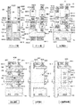
図1は、本発明の第1実施形態に係る電気光学装置1の構成を示す斜視図である。電気光学装置1は、例えばヘッドマウント・ディスプレイにおいて画像を表示するマイクロ・ディスプレイである。
<First embodiment>
FIG. 1 is a perspective view illustrating a configuration of an electro-
図1に示すように、電気光学装置1は、表示パネル2と、表示パネル2の動作を制御する制御回路3とを備える。表示パネル2は、複数の画素回路と、当該画素回路を駆動する駆動回路とを備える。本実施形態において、表示パネル2が備える複数の画素回路及び駆動回路は、シリコン基板に形成され、画素回路には、発光素子の一例であるOLEDが用いられる。また、表示パネル2は、例えば、表示部で開口する枠状のケース82に収納されるとともに、FPC(Flexible Printed Circuits)基板84の一端が接続される。
As shown in FIG. 1, the electro-
FPC基板84には、半導体チップの制御回路3が、COF(Chip On Film)技術によって実装されるとともに、複数の端子86が設けられて、図示省略された上位回路に接続される。
The
図2は、実施形態に係る電気光学装置1の構成を示すブロック図である。上述のとおり、電気光学装置1は、表示パネル2と、制御回路3とを備える。
FIG. 2 is a block diagram illustrating a configuration of the electro-
制御回路3には、図示省略された上位回路よりデジタルの画像データVdataが同期信号に同期して供給される。ここで、画像データVdataとは、表示パネル2(厳密には、後述する表示部100)で表示すべき画像の画素の階調レベルを例えば8ビットで規定するデータである。また、同期信号とは、垂直同期信号、水平同期信号、及び、ドットクロック信号を含む信号である。
Digital image data Vdata is supplied to the
制御回路3は、同期信号に基づいて、各種制御信号を生成し、これを表示パネル2に対して供給する。具体的には、制御回路3は、表示パネル2に対して、制御信号Ctrと、正論理の制御信号Giniと、これと論理反転の関係にある負論理の制御信号/Giniと、正論理の制御信号Gcplと、これと論理反転の関係にある負論理の制御信号/Gcplと、制御信号Sel(1)、Sel(2)、Sel(3)と、これらの信号に対して論理反転の関係にある制御信号/Sel(1)、/Sel(2)、/Sel(3)と、を供給する。
The
ここで、制御信号Ctrとは、パルス信号や、クロック信号、イネーブル信号など、複数の信号を含む信号である。 Here, the control signal Ctr is a signal including a plurality of signals such as a pulse signal, a clock signal, and an enable signal.
なお、制御信号Sel(1)、Sel(2)、Sel(3)を、制御信号Selと総称し、制御信号/Sel(1)、/Sel(2)、/Sel(3)を、制御信号/Selと総称する場合がある。 The control signals Sel (1), Sel (2), and Sel (3) are collectively referred to as a control signal Sel, and the control signals / Sel (1), / Sel (2), and / Sel (3) are / Sel.
また、制御回路3は電圧生成回路31を含む。電圧生成回路31は、表示パネル2に対して、各種電位を供給する。具体的には、制御回路3は、表示パネル2に対してリセット電位Vorst及び初期電位Vini等を供給する。
Further, the
さらに、制御回路3は、画像データVdataに基づいて、アナログの画像信号Vidを生成する。具体的には、制御回路3には、画像信号Vidの示す電位、及び、表示パネル2が備える発光素子(後述するOLED130)の輝度を対応付けて記憶したルックアップテーブルが設けられる。そして、制御回路3は、当該ルックアップテーブルを参照することで、画像データVdataに規定される発光素子の輝度に対応した電位を示す画像信号Vidを生成し、これを表示パネル2に対して供給する。
Further, the
図2に示すように、表示パネル2は、表示部100と、これを駆動する駆動回路(データ転送線駆動回路5及び走査線駆動回路6)とを備える。
As shown in FIG. 2, the
表示部100には、表示すべき画像の画素に対応した画素回路110がマトリクス状に配列されている。詳細には、表示部100において、M行の走査線12が図において横方向(X方向)に延在して設けられ、また、3列毎にグループ化された(3N)列の第1データ転送線14−1が図において縦方向(Y方向)に延在し、かつ、各走査線12と互いに電気的な絶縁を保って設けられている。
In the
なお、図面の煩雑化を避けるために図2においては図示していないが、各々の第1データ転送線14−1に対しては、第2データ転送線14−2が電気的に接続可能に且つ縦方向(Y方向)に延在して設けられている(例えば図4参照)。そして、M行の走査線12と、(3N)列の第2データ転送線14−2とに対応して画素回路110が設けられている。このため、本実施形態において画素回路110は、縦M行×横(3N)列でマトリクス状に配列されている。
Although not shown in FIG. 2 in order to avoid complication of the drawing, a second data transfer line 14-2 can be electrically connected to each first data transfer line 14-1. In addition, they are provided to extend in the vertical direction (Y direction) (for example, see FIG. 4). The
ここで、M、Nは、いずれも自然数である。走査線12及び画素回路110のマトリクスのうち、行(ロウ)を区別するために、図において上から順に1、2、3、…、(M−1)M行と呼ぶ場合がある。同様に第1データ転送線14−1及び画素回路110のマトリクスの列(カラム)を区別するために、図において左から順に1、2、3、…、(3N−1)、(3N)列と呼ぶ場合がある。
Here, M and N are both natural numbers. .., (M−1) M rows may be referred to from the top in order to distinguish rows in the matrix of the
ここで、第1データ転送線14−1のグループを一般化して説明するために、1以上の任意の整数をnと表すと、左から数えてn番目のグループには、(3n−2)列目、(3n−1)列目及び(3n)列目の第1データ転送線14−1が属している、ということになる。 Here, in order to generalize and describe the group of the first data transfer lines 14-1, if an arbitrary integer equal to or greater than 1 is represented by n, the (n) th group counted from the left includes (3n-2) This means that the first data transfer line 14-1 in the (3n-1) th and (3n) th columns belongs to the column.
なお、同一行の走査線12と、同一グループに属する3列の第2データ転送線14−2とに対応した3つの画素回路110は、それぞれR(赤)、G(緑)、B(青)の画素に対応して、これらの3画素が表示すべきカラー画像の1ドットを表現する。すなわち、本実施形態では、RGBに対応したOLEDの発光によって1ドットのカラーを加法混色で表現する構成となっている。
The three
また、図2に示すように、表示部100において、(3N)列の給電線(リセット電位供給線)16が、縦方向に延在し、かつ、各走査線12と互いに電気的な絶縁を保って設けられる。各給電線16には、所定のリセット電位Vorstが共通に給電されている。ここで、給電線16の列を区別するために、図において左から順に1、2、3、…、(3N)列目の給電線16と呼ぶ場合がある。1列目〜(3N)列目の給電線16の各々は、1列目〜(3N)列目の第1データ転送線14−1(第2データ転送線14−2)の各々に対応して設けられる。
Further, as shown in FIG. 2, in the
走査線駆動回路6は、1個のフレームの期間内にM本の走査線12を1行毎に順番に走査するための走査信号Gwrを、制御信号Ctrに従って生成する。ここで、1、2、3、…、M行目の走査線12に供給される走査信号Gwrを、それぞれGwr(1)、Gwr(2)、Gwr(3)、…、Gwr(M-1)、Gwr(M)と表記している。
The scanning
なお、走査線駆動回路6は、走査信号Gwr(1)〜Gwr(M)のほかにも、当該走査信号Gwrに同期した各種制御信号を行毎に生成して表示部100に供給するが、図2においては図示を省略している。また、フレームの期間とは、電気光学装置1が1カット(コマ)分の画像を表示するのに要する期間をいい、例えば同期信号に含まれる垂直同期信号の周波数が120Hzであれば、その1周期分の8.3ミリ秒の期間である。
The scanning
データ転送線駆動回路5は、(3N)列の第1データ転送線14−1の各々と1対1に対応して設けられる(3N)個のデータ転送回路DT、各グループを構成する3列の第1データ転送線14−1毎に設けられるN個のデマルチプレクサDM、及び、データ信号供給回路70を備える。
The data transfer
データ信号供給回路70は、制御回路3より供給される画像信号Vidと制御信号Ctrとに基づいて、データ信号Vd(1)、Vd(2)、…、Vd(N)を生成する。すなわち、データ信号供給回路70は、データ信号Vd(1)、Vd(2)、…、Vd(N)を時分割多重した画像信号Vidに基づいて、データ信号Vd(1)、Vd(2)、…、Vd(N)を生成する。そして、データ信号供給回路70は、データ信号Vd(1)、Vd(2)、…、Vd(N)を、1、2、…、N番目のグループに対応するデマルチプレクサDMに対して、それぞれ供給する。
The data signal
図3は、デマルチプレクサDMとデータ転送回路DTとの構成を説明するための回路図である。なお、図3は、n番目のグループに属するデマルチプレクサDMと、当該デマルチプレクサDMに接続された3個のデータ転送回路DTとを、代表的に表している。なお、以下では、n番目のグループに属するデマルチプレクサDMを、DM(n)と表記する場合がある。 FIG. 3 is a circuit diagram for explaining the configuration of the demultiplexer DM and the data transfer circuit DT. FIG. 3 representatively shows a demultiplexer DM belonging to the n-th group and three data transfer circuits DT connected to the demultiplexer DM. Hereinafter, the demultiplexer DM belonging to the n-th group may be referred to as DM (n).
以下では、図2に加えて図3を参照しながら、デマルチプレクサDM及びデータ転送回路DTの構成について説明する。 Hereinafter, the configurations of the demultiplexer DM and the data transfer circuit DT will be described with reference to FIG. 3 in addition to FIG.
図3に示すように、デマルチプレクサDMは、列毎に設けられたトランスミッションゲート34の集合体であり、各グループを構成する3列に、データ信号を順番に供給するものである。ここで、n番目のグループに属する(3n−2)、(3n−1)、(3n)列に対応したトランスミッションゲート34の入力端は互いに共通接続されて、その共通端子にそれぞれデータ信号Vd(n)が供給される。n番目のグループにおいて左端列である(3n−2)列に設けられたトランスミッションゲート34は、制御信号Sel(1)がHレベルであるとき(制御信号/Sel(1)がLレベルであるとき)にオン(導通)する。同様に、n番目のグループにおいて中央列である(3n−1)列に設けられたトランスミッションゲート34は、制御信号Sel(2)がHレベルであるとき(制御信号/Sel(2)がLレベルであるとき)にオンし、n番目のグループにおいて右端列である(3n)列に設けられたトランスミッションゲート34は、制御信号Sel(3)がHレベルであるとき(制御信号/Sel(3)がLレベルであるとき)にオンする。
As shown in FIG. 3, the demultiplexer DM is an aggregate of
データ転送回路DTは、保持容量(第3容量)41、トランスミッションゲート45、及び、トランスミッションゲート42の組を列毎に有し、後述する初期化期間および補償期間において各列のトランスミッションゲート34の出力端から出力されるデータ信号の電位を保持容量(第3容量)41に蓄積し、後述する書込期間において保持容量(第3容量)41に蓄積されたデータ信号の電位を、転送容量133に転送する回路である。
The data transfer circuit DT has a set of a storage capacitor (third capacitor) 41, a
各列のトランスミッションゲート45のソース又はドレインは、第1データ転送線14−1に電気的に接続される。また、制御回路3は、各列のトランスミッションゲート45のゲートに対して、制御信号/Giniを共通に供給する。トランスミッションゲート45は、第1データ転送線14−1と、初期電位Viniの供給線とを、制御信号/GiniがLレベルのときに電気的に接続し、制御信号/GiniがHレベルのときに電気的に非接続とする。なお、初期電位Viniの供給線61には、制御回路3から所定の初期電位Viniが供給される。
The source or drain of the
保持容量41は2つの電極を有する。保持容量41の一方の電極は、ノードhを介してトランスミッションゲート42の入力端に電気的に接続される。また、トランスミッションゲート42の出力端は、第1データ転送線14−1に電気的に接続される。
The
制御回路3は、各列のトランスミッションゲート42に対して、制御信号Gcpl及び制御信号/Gcplを共通に供給する。このため、各列のトランスミッションゲート42は、制御信号GcplがHレベルであるとき(制御信号/GcplがLレベルであるとき)に一斉にオンする。
The
各列の保持容量41の一方の電極は、ノードhを介して、トランスミッションゲート34の出力端、及び、トランスミッションゲート42の入力端に電気的に接続される。そして、トランスミッションゲート34がオンした際、保持容量41の一方の電極には、トランスミッションゲート34の出力端を介してデータ信号Vd(n)が供給される。すなわち、保持容量41は、一方の電極にデータ信号Vd(n)が供給される。
One electrode of the
また、各列の保持容量41の他方の電極は、固定電位である電位Vssが供給される給電線63に共通に接続される。ここで、電位Vssは、論理信号である走査信号や制御信号のLレベルに相当するものであってもよい。なお、保持容量41の容量値をCrfとする。
The other electrode of the
図4を参照して、画素回路110等について説明する。画素回路110が配列する行を一般的に示すために、1以上M以下の任意の整数をmと表す。また、1以上M以下であって、連続する任意の整数をm1、m2と表す。すなわち、mは、m1やm2を包含する一般化した概念である。
The
各画素回路110については電気的にみれば互いに同一構成なので、ここでは、m行目に位置し、且つ、n番目のグループのうち左端列の(3n−2)列目に位置する、m行(3n−2)列の画素回路110を例にとって説明する。
Since each
図4に示されるように、第1データ転送線14−1には転送容量(第1容量)133の第1電極133−1と、第1トランジスター126のソース又はドレインの一方とが電気的に接続されている。また、転送容量133の第2電極133−2と、第1トランジスター126のソース又はドレインの他方とは、第2データ転送線14−2に電気的に接続されている。
As shown in FIG. 4, the first electrode 133-1 of the transfer capacitor (first capacitor) 133 and one of the source and the drain of the
つまり、第1データ転送線14−1と第2データ転送線14−2との間には、転送容量133と第1トランジスター126とが並列に接続される。
That is, the
また、画素回路110は、第2データ転送線14−2に対して接続される。すなわち、画素回路110には、第1データ転送線14−1及び第2データ転送線14−2を介して、指定階調に応じた階調電位が供給される。
The
本実施形態においては、一本の第2データ転送線14−2に対して1個の画素回路110が電気的に接続される。
In the present embodiment, one
但し、本発明はこのような構成に限定されるものではなく、一本の第2データ転送線14−2に対してNb個の画素回路110を電気的に接続してもよい。つまり、複数個の画素回路110が、一本の第2データ転送線14−2と、一つの転送容量133と、第1トランジスター126とを共用するようにしてもよい。
However, the present invention is not limited to such a configuration, and
図5は、本実施形態に特有の構成を説明する図である。本実施形態では、第1データ転送線14−1には、図5に示すように二以上の第2データ転送線14−2が、それぞれ転送容量133を介して接続される。
FIG. 5 is a diagram illustrating a configuration unique to the present embodiment. In the present embodiment, as shown in FIG. 5, two or more second data transfer lines 14-2 are connected to the first data transfer line 14-1 via the
ここで、第2データ転送線14−2と転送容量133とを介して、同一の第1データ転送線14−1に接続された画素回路110の集合を「画素列」と称する(図5における画素列P)。また、所定数の画素回路110の集合を「ブロック」と称する(図5におけるブロックB)。
Here, a set of
図5に示すように、画素列Pは複数のブロックBを含み、各ブロックBは複数の画素回路110を含む。つまり、本実施形態においては、第2データ転送線14−2は、画素列Pに含まれる画素回路110の個数と等しい個数の画素回路110に対して設けられている。
As shown in FIG. 5, the pixel column P includes a plurality of blocks B, and each block B includes a plurality of
これに対して、従来の構成は図6に示すものである。図6は、比較例として示す従来の構成を説明する図である。同図に示すように、従来の構成では、第2データ転送線14−2が画素列Pに対して設けられ、その端部に転送容量133と第1データ転送線14−1とが設けられている。つまり、従来の構成では、一の画素列P(に含まれる全ての画素回路110)に対して、一本の第1データ転送線14−1と一本の第2データ転送線14−2とが設けられている。この点が、図5を参照して説明した本実施形態に特有の構成、すなわち第2データ転送線14−2が画素列Pを構成するブロックB単位で分割されて複数設けられている点と明確に相違する。
On the other hand, the conventional configuration is shown in FIG. FIG. 6 is a diagram illustrating a conventional configuration shown as a comparative example. As shown in the figure, in the conventional configuration, a second data transfer line 14-2 is provided for the pixel column P, and a
ところで、下記の(式1)で示されるように、表示部100における画素回路110の全行数Mを、一本の第2データ転送線14−2に接続された画素回路110の行数Nbで除した値をKとする。換言すれば、第2データ転送線14−2は、MをNbで除した値であるK本に分割され、1本の第2データ転送線14−2にはNb個の画素回路110が接続されてなるとする。
By the way, as shown in (Equation 1) below, the total number M of rows of the

本実施形態では、一本の第1データ転送線14−1に対して、K(K≧2)×Nb本の第2データ転送線14−2が設けられている。換言すれば、一の画素列Pは、K個のブロックBを備える。また、第1データ転送線14−1は、M行分(M個)の画素回路110に対応して設けられ、第2データ転送線14−2は、Nb行分(Nb個)の画素回路110に対応して設けられる。従って、第2データ転送線14−2は第1データ転送線14−1と比較して短い。
In the present embodiment, K (K ≧ 2) × Nb second data transfer lines 14-2 are provided for one first data transfer line 14-1. In other words, one pixel column P includes K blocks B. The first data transfer lines 14-1 are provided corresponding to the M rows (M) of
本実施形態では、Nbの値は1である。なお、1以上K以下の任意の整数として、kを用いる。 In the present embodiment, the value of Nb is 1. Note that k is used as an arbitrary integer of 1 or more and K or less.
以降、1行目から数えてm番目の行における各画素回路110に対応する第1トランジスター126は、1行目から数えてm番目の第1トランジスター126であるとし、制御信号Gfix(m)が供給されるとする。
Hereinafter, it is assumed that the
画素回路110は、PチャネルMOS型のトランジスター121〜125と、OLED130と、画素容量132と、を含む。m行目の画素回路110には、走査信号Gwr(m)、制御信号Gcmp(m)、Gel(m)、Gorst(m)が供給される。ここで、走査信号Gwr(m)、制御信号Gcmp(m)、Gel(m)、Gorst(m)は、それぞれm行目に対応して走査線駆動回路6によって供給されるものである。
The
なお、図2では図示省略したが、図4に示すように表示パネル2(表示部100)には、横方向(X方向)に延在するM行の制御線143(第1制御線)、横方向に延在するM行の制御線144(第2制御線)、横方向に延在するM行の制御線145(第3制御線)、横方向に延在するK行の制御線146(第4制御線)が設けられる。
Although not shown in FIG. 2, as shown in FIG. 4, the display panel 2 (display unit 100) includes M rows of control lines 143 (first control lines) extending in the horizontal direction (X direction). Control lines 144 (second control lines) of M rows extending in the horizontal direction, control lines 145 (third control lines) of M rows extending in the horizontal direction,
そして、走査線駆動回路6は、m行目の制御線143に対して制御信号Gcmp(m)を供給し、m行目の制御線144に対して制御信号Gel(m)を供給し、m行目の制御線145に対して制御信号Gorst(m)を供給し、m行目の制御線146に対して制御信号Gfix( m)を供給する。
Then, the scanning
すなわち、走査線駆動回路6は、m行目に位置する画素回路に対して、走査信号Gwr(m)、制御信号Gel(m)、Gcmp(m)、Gorst(m)を、それぞれ、m行目の走査線12、制御線143、144、145を介して供給する。また、m行目に位置する第1トランジスター126に対して制御信号Gfix( m)を、m行目の制御線146を介して供給する。
That is, the scanning
以下では、走査線12、制御線143、制御線144、制御線145、及び制御線146を、「制御線」と総称する場合がある。すなわち、本実施形態に係る表示パネル2には、各行に走査線12を含む4本の制御線が設けられると共に、1行ごとに1本の制御線146が設けられる。
Hereinafter, the
画素容量132、及び転送容量133は、それぞれ2つの電極を有する。転送容量133は、第1電極133−1と第2電極133−2とを含む静電容量である。
Each of the
第2トランジスター122は、ゲートがm行目の走査線12に電気的に接続され、ソース又はドレインの一方が、第2データ転送線14−2に電気的に接続されている。また、第2トランジスター122は、ソースまたはドレインの他方が、駆動トランジスター121のゲートと、画素容量132の一方の電極とに、それぞれ電気的に接続されている。すなわち、第2トランジスター122は、駆動トランジスター121のゲートと転送容量133の第2電極133−2との間に電気的に接続されている。そして、第2トランジスター122は、駆動トランジスター121のゲートと、(3n−2)列目の第2データ転送線14−2に接続された転送容量133の第2電極133−2との間の電気的な接続を制御するトランジスターとして機能する。
The gate of the
駆動トランジスター121は、そのソースが給電線116に電気的に接続され、そのドレインは、第3トランジスター123のソースまたはドレインの一方と、第4トランジスター124のソースとに電気的に接続されている。
The driving
ここで、給電線116には、画素回路110において電源の高位側となる電位Velが給電される。この駆動トランジスター121は、駆動トランジスター121のゲート及びソース間の電圧に応じた電流を流す駆動トランジスターとして機能する。
Here, the
第3トランジスター123は、ゲートが制御線143に電気的に接続され、制御信号Gcmp(m)が供給される。この第3トランジスター123は、駆動トランジスター121のゲートとドレインとの間の電気的な接続を制御するスイッチングトランジスターとして機能する。よって、第3トランジスター123は、第2トランジスター122を介して駆動トランジスター121のゲート及びドレインの間を導通させるためのトランジスターである。なお、第3トランジスター123のソース及びドレインの一方と駆動トランジスター121のゲートとの間には第2トランジスター122が接続されているが、第3トランジスター123のソース及びドレインの一方は、駆動トランジスター121のゲートに電気的に接続されているとも解釈され得る。
The
第4トランジスター124は、ゲートが制御線144に電気的に接続され、制御信号Gel(m)が供給される。また、第4トランジスター124は、ドレインが第5トランジスター125のソースとOLED130のアノード130aとにそれぞれ電気的に接続されている。この第4トランジスター124は、駆動トランジスター121のドレインと、OLED130のアノードとの間の電気的な接続を制御する、スイッチングトランジスターとして機能する。さらに、駆動トランジスター121のドレインとOLED130のアノードとの間には第4トランジスター124が接続されているが、駆動トランジスター121のドレインは、OLED130のアノードに電気的に接続されているとも解釈され得る。
The
第5トランジスター125は、ゲートが制御線145に電気的に接続され、制御信号Gorst(m)が供給される。また、第5トランジスター125のドレインは(3n−2)列目の給電線16に電気的に接続されてリセット電位Vorstに保たれている。この第5トランジスター125は、給電線16と、OLED130のアノード130aとの間の電気的な接続を制御するスイッチングトランジスターとして機能する。
The
第1トランジスター126は、ゲートが制御線146に電気的に接続され、制御信号Gfix(k)が供給される。また、第1トランジスター126は、ソース又はドレインの一方が、第2データ転送線14−2と電気的に接続され、第2データ転送線14−2を介して転送容量133の第2電極133−2及び第3トランジスター123のソース又はドレインの他方に電気的に接続されている。また、第1トランジスター126は、ソース又はドレインの他方が、(3n−2)列目の第1データ転送線14−1と電気的に接続されている。
The
この第1トランジスター126は、主として、第1データ転送線14−1と第2データ転送線14−2との間の電気的な接続を制御するスイッチングトランジスターとして機能する。
The
ここで、第1トランジスター126及び転送容量133は、同一の第2データ転送線14−2に接続されているNb個の画素回路110によって共用される。本実施形態では、図4に示すように、1本の同一の第2データ転送線14−2には各行目の画素回路110が接続される。
Here, the
なお、本実施形態において表示パネル2はシリコン基板に形成されるので、トランジスター121〜126の基板電位については電位Velとしている。また、上記におけるトランジスター121〜126のソース、ドレインは、トランジスター121〜126のチャネル型、電位の関係に応じて入れ替わってもよい。また、トランジスターは薄膜トランジスターであっても電界効果トランジスターであってもよい。
In this embodiment, since the
画素容量132は、一方の電極が駆動トランジスター121のゲートgに電気的に接続され、他方の電極が給電線116に電気的に接続される。このため、画素容量132は、駆動トランジスター121のゲート・ソース間の電圧を保持する保持容量として機能する。なお、画素容量132の容量値をCpixと表記する。
The
なお、画素容量132としては、駆動トランジスター121のゲートgに寄生する容量を用いても良いし、シリコン基板において互いに異なる導電層で絶縁層を挟持することによって形成される容量を用いても良い。
Note that as the
転送容量133は、第1電極133−1が第1データ転送線14−1及びトランスミッションゲート42を介して保持容量41の一方の電極に電気的に接続される。また、転送容量133は、第2電極133−2が第2データ転送線14−2及び第2トランジスター122を介して駆動トランジスター121のゲートgに電気的に接続される。このため、転送容量133は、後述する補償期間において、ゲートgの電位を、第1データ転送線14−1及び第1電極133−1の電位の変化量に対して、転送容量133と保持容量41との容量比を乗じた値だけレベルシフトさせる転送容量として機能する。詳しくは後述する。なお、転送容量133の容量値をC1と表記する。
In the
また、本実施形態においては、リセット電位Vorstが供給される給電線16と、第1データ転送線14−1との間には、シールド容量134が設けられている。転送容量133は、第1電極134−1と第2電極134−2とを含む静電容量である。シールド容量134は、第1データ転送線14−1をシールドするシールド容量として機能する。なお、シールド容量134の容量値をC2と表記する。
In the present embodiment, a
OLED130のアノード130aは、画素回路110毎に個別に設けられる画素電極である。これに対して、OLED130のカソードは、画素回路110のすべてにわたって共通に設けられる共通電極118であり、画素回路110において電源の低位側となる電位Vctに保たれている。OLED130は、上記シリコン基板において、アノード130aと光透過性を有するカソードとで白色有機EL層を挟持した素子である。そして、OLED130の出射側(カソード側)にはRGBのいずれかに対応したカラーフィルターが重ねられる。なお、白色有機EL層を挟んで配置される2つの反射層間の光学距離を調整してキャビティ構造を形成し、OLED130から発せられる光の波長を設定してもよい。この場合、カラーフィルターを有していてもよいし、有さなくてもよい。
The
このようなOLED130において、アノード130aからカソードに電流が流れると、アノード130aから注入された正孔とカソードから注入された電子とが有機EL層で再結合して励起子が生成され、白色光が発生する。このときに発生した白色光は、シリコン基板(アノード130a)とは反対側のカソードを透過し、カラーフィルターによる着色を経て、観察者側に視認される構成となっている。
In such an
図7を参照して電気光学装置1の動作について説明する。図7は、電気光学装置1における各部の動作を説明するためのタイミングチャートである。この図に示されるように、走査線駆動回路6は、走査信号Gwr(1)〜Gwr(M)を順次Lレベルに切り替えて、1フレームの期間において1〜M行目の走査線12を1水平走査期間(H)毎に順番に走査する。
The operation of the electro-
1水平走査期間(H)での動作は、各行の画素回路110にわたって共通である。そこで以下については、m1行目が水平走査される水平走査期間において、特にm1行(3n−2)列の画素回路110について着目して動作を説明する。
The operation in one horizontal scanning period (H) is common to the
本実施形態ではm1行目の水平走査期間は、大別すると、図7において(a)で示される初期化期間と、(b)で示される補償期間と、(c)で示される書込期間と、(d)で示される非発光期間とに分けられる。また、次の水平走査期間は、(d)で示される非発光期間が継続し、さらに次の水平走査期間は、(e)で示される発光期間となり、1フレームの期間経過後に再びm1行目の水平走査期間に至る。このため、時間の順でいえば、初期化期間→補償期間→書込期間→非発光期間→発光期間というサイクルの繰り返しとなる。 In this embodiment, the horizontal scanning period of the m1th row is roughly divided into an initialization period shown in FIG. 7A, a compensation period shown in FIG. 7B, and a writing period shown in FIG. And a non-light emitting period shown in (d). In the next horizontal scanning period, the non-light emitting period shown in (d) continues, and in the next horizontal scanning period, the light emitting period shown in (e) is reached, and after the period of one frame elapses, the m1th row is returned again. In the horizontal scanning period. Therefore, in the order of time, the cycle of the initialization period → the compensation period → the writing period → the non-light emitting period → the light emitting period is repeated.
図8は、発光期間における画素回路110などの動作を説明する図である。なお、図8においては、動作説明で重要となる電流経路を太線で示し、オフ状態のトランジスター又はトランスミッションゲート上には太線で「X」印を付している(以下の図9、図10、図11、及び図14においても同様である)。
FIG. 8 is a diagram illustrating the operation of the
<初期化期間>
図7に示されるように、m1行目の初期化期間では、走査信号Gwr(m1)はHレベルであり、制御信号Gel(m1)はHレベルであり、制御信号Gcmp(m1)はHレベルであり、制御信号Gfix(m1)はLレベルである。制御信号Gorst(m1)はLレベルである。
<Initialization period>
As shown in FIG. 7, in the initialization period of the m1th row, the scanning signal Gwr (m1) is at the H level, the control signal Gel (m1) is at the H level, and the control signal Gcmp (m1) is at the H level. And the control signal Gfix (m1) is at the L level. The control signal Gorst (m1) is at the L level.
このため、図8に示されるように、m1行(3n−2)列の画素回路110においては第5トランジスター125,第1トランジスター126がオンする一方、駆動トランジスター121、第2トランジスター122、第3トランジスター123、第4トランジスター124がオフする。これにより、OLED130に供給される電流の経路が遮断されるので、OLED130は、オフ(非発光)状態となる。
Therefore, as shown in FIG. 8, in the
図8に示されるように、第5トランジスタートランジスター125がオンすることにより、OLED130のアノード130aと給電線16とが電気的に接続され、アノード130aの電位がリセット電位Vorstに設定される
As shown in FIG. 8, when the
ここで、初期化期間においてデータ転送回路DTでは、制御信号/GiniがLレベルになり、制御信号GiniがHレベルになるので図8に示されるようにトランスミッションゲート45がオンし、制御信号GcplがLレベルになり、制御信号/GcplがHレベルになるので図8に示されるようにトランスミッションゲート42がオフする。また、制御信号Gfix(k)はLレベルであるため、第1トランジスター126がオンしている。このため、図8に示されるように転送容量133の第1電極133−1に接続された第1データ転送線14−1が初期電位Viniに設定されると共に、第1データ転送線14−1と第2データ転送線14−2とが電気的に接続され、転送容量133の第2電極133−2も初期電位Viniに設定される。これにより、転送容量133が初期化される。
Here, in the data transfer circuit DT during the initialization period, the control signal / Gini becomes L level and the control signal Gini becomes H level, so that the
また、初期化期間におけるデマルチプレクサDM(n)では、制御信号Sel(1)がHレベルになり、制御信号/Sel(1)がLレベルになるので、図8に示されるようにトランスミッションゲート34がオンする。これにより、容量値Crfの保持容量41に階調電位が書き込まれる。
Further, in the demultiplexer DM (n) during the initialization period, the control signal Sel (1) goes high and the control signal / Sel (1) goes low, so that the
ところで、本実施形態では、m1行(3n−2)列の画素回路110が接続されている第2データ転送線14−2と、m2行(3n−2)列の画素回路110が接続されている第2データ転送線14−2とは別になっている。従って、m1行目の初期化期間には制御信号Gfix(m1)によって制御される第1トランジスター126が用いられ、図9に示されるようにm2行目の初期化期間には制御信号Gfix(m2)によって制御される第1トランジスター126が用いられる。
In the present embodiment, the second data transfer line 14-2 to which the
<補償期間>
初期化期間を終えると補償期間が開始する。m1行目の補償期間では、走査信号Gwr(m1)はLレベルであり、制御信号Gel(m1)はHレベルであり、制御信号Gcmp(m1)はLレベルであり、制御信号Gfix(m1)はHレベルである。制御信号Gorst(m1)はLレベルである。
<Compensation period>
After the initialization period, the compensation period starts. In the compensation period of the m1th row, the scanning signal Gwr (m1) is at the L level, the control signal Gel (m1) is at the H level, the control signal Gcmp (m1) is at the L level, and the control signal Gfix (m1) Is at the H level. The control signal Gorst (m1) is at the L level.
このため、図10に示されるように、m1行(3n−2)列の画素回路110においては第2トランジスター122、第3トランジスター123、第5トランジスター125がオンする一方、第4トランジスター124、第1トランジスター126がオフする。このとき、駆動トランジスター121のゲートgは、第2トランジスター122と第3トランジスター123とを介して自身のドレインに接続(ダイオード接続)され、駆動トランジスター121にはドレイン電流が流れてゲートgを充電する。
Therefore, as shown in FIG. 10, in the
すなわち、駆動トランジスター121のドレインとゲートgとは、第2データ転送線14−2に接続され、駆動トランジスター121の閾値電圧をVthとすると、駆動トランジスター121のゲートgの電位Vgは、(Vel−Vth)に漸近していく。
That is, the drain and gate g of the driving
ここで、補償期間のデータ転送回路DTにおいては、制御信号/GiniがLレベルになり、制御信号GiniがHレベルになるので、図10に示されるようにトランスミッションゲート45がオンし、制御信号GcplがLレベルになり、制御信号/GcplがHレベルになるので、トランスミッションゲート42がオフする。このとき、上述したように従来の構成と比較して第2データ転送線14−2が短いため、第2データ転送線14−2に付随する寄生容量への充電又は放電に要する時間が短縮され、補償期間自体が短縮される。
Here, in the data transfer circuit DT during the compensation period, the control signal / Gini goes low and the control signal Gini goes high, so that the
また、補償期間におけるデマルチプレクサDM(n)では、制御信号Sel(1)がHレベルになり、制御信号/Sel(1)がLレベルになるので、図10に示されるようにトランスミッションゲート34がオンする。これにより、容量値Crfの保持容量41に階調電位が書き込まれる。
Also, in the demultiplexer DM (n) during the compensation period, the control signal Sel (1) goes high and the control signal / Sel (1) goes low, so that the
なお、第4トランジスター124はオフしているため、駆動トランジスター121のドレインはOLED130と電気的に非接続である。また、初期化期間と同様、第5トランジスター125がオンすることによって、OLED130のアノード130aと給電線16とが電気的に接続され、アノード130aの電位がリセット電位Vorstに設定される。
Since the
<書込期間>
補償期間を終えると、書込期間が開始する。m1行目の書込期間では、走査信号Gwr(m1)がLレベルであり、制御信号Gel(m1)はHレベルであり、制御信号Gcmp(m1)はHレベルであり、制御信号Gfix(m1)はHレベルである。制御信号Gorst(m1)はLレベルである。
<Write period>
When the compensation period ends, the writing period starts. In the writing period of the m1th row, the scanning signal Gwr (m1) is at the L level, the control signal Gel (m1) is at the H level, the control signal Gcmp (m1) is at the H level, and the control signal Gfix (m1). ) Is the H level. The control signal Gorst (m1) is at the L level.
このため、図11に示されるように、m1行(3n−2)列の画素回路110においてはトランジスター122、125がオンする一方、トランジスター123、124、126がオフする。
Therefore, as shown in FIG. 11, in the
ここで、書込期間のデータ転送回路DTにおいては、制御信号/GiniがHレベルになるので、図11に示されるようにトランスミッションゲート45がオフし、制御信号GcplがHレベルになるので、図11に示されるようにトランスミッションゲート42がオンする。このため、第1データ転送線14−1及び第1電極133−1への初期電位Viniの供給が解除されると共に、第1データ転送線14−1及び第1電極133−1に対して容量値Crfの保持容量41の一方の電極が接続され、当該第1電極133−1に階調電位が供給される。そして、階調電位がレベルシフトされた信号が、駆動トランジスター121のゲートに供給され、画素容量132に書き込まれる。このように、本実施形態においては、データ転送回路DTのトランスミッションゲート42および保持容量41、並びに転送容量133を用いて階調電位のレベルシフトが行われる。
Here, in the data transfer circuit DT during the writing period, since the control signal / Gini goes high, the
なお、書込期間におけるデマルチプレクサDM(n)では、制御信号Sel(1)がLレベルになるので、図11に示されるようにトランスミッションゲート34がオフする。
In the demultiplexer DM (n) during the writing period, the control signal Sel (1) goes low, so that the
なお、第4トランジスター124はオフしているため、駆動トランジスター121のドレインはOLED130と電気的に非接続である。また、初期化期間と同様、第5トランジスター125がオンすることによって、OLED130のアノード130aと給電線16とが電気的に接続され、アノード130aの電位がリセット電位Vorstに初期化される。
Since the
なお、m行目の書込期間が開始されるまで(初期化期間、補償期間の間)に、制御回路3は、n番目のグループでいえば、データ信号Vd(n)を順番に、m行(3n−2)列、m行(3n−1)列、m行(3n)列の画素の階調レベルに応じた電位に切り替える。
Before the writing period of the m-th row is started (during the initialization period and the compensation period), the
一方、制御回路3は、データ信号の電位の切り替えに合わせて制御信号Sel(1)、Sel(2)、Sel(3)を順番に排他的にHレベルとする。制御回路3は、図示は省略しているが、制御信号Sel(1)、Sel(2)、Sel(3)とは論理反転の関係にある制御信号/Sel(1)、/Sel(2)、/Sel(3)についても出力している。これによって、デマルチプレクサDMでは、各グループにおいてトランスミッションゲート34がそれぞれ左端列、中央列、右端列の順番でオンする。
On the other hand, the
ところで、左端列のトランスミッションゲート34が制御信号Sel(1)、/Sel(1)によってオンしたとき、第1データ転送線14−1及び第1電極133−1の電位の変化量をΔVとすると、第2データ転送線14−2及び駆動トランジスター121のゲートgの電位の変化量ΔVgは、下記(式2)で表せる。但し、転送容量133の容量値C1は画素回路110の行数に比例して容量値を調整可能であり、1行当たりの容量C1aとする。また、1行当たりの第2データ転送線14−2に付随する寄生容量の容量値をC3aとする。また、上述したように、一本の第2データ転送線14−2に接続された画素回路110の行数をNbと表す。
By the way, when the
ここでΔVとΔVgとの比を、下記の(式3)で示すように圧縮率Rとする。
Here, the ratio between ΔV and ΔVg is defined as a compression ratio R as shown in the following (Equation 3).
つまり、書込期間における駆動トランジスター121のゲートgの電位Vgは、補償期間における電位Vgから、第1データ転送線14−1及び第1電極133−1の電位の変化量ΔVに対して、Rを乗じた値だけレベルシフトした(データ圧縮された)値となる。この書込期間を終えると、後述する発光期間が開始する。
In other words, the potential Vg of the gate g of the driving
上述した(式2)に示される関係から、一本の第2データ転送線14−2に対して接続する画素回路110の個数Nbが多いほど(1ブロック内に含まれる画素回路110の個数Nbが多いほど)、ΔVgとΔVとは近い値になる。換言すれば、Nbの値が大きいほど、(式4)に示すRは1に近づく。
From the relationship shown in the above (Equation 2), the larger the number Nb of the
ここで、第2データ転送線14−2に接続する画素回路110の個数Nb(1ブロック内に含まれる画素回路110の個数Nb)は、補償動作の完了に要する時間と、データ圧縮の圧縮率と、を鑑みて決定することが好ましい。以下、具体的に説明する。
Here, the number Nb of the
まず、補償動作の完了に要する時間について説明する。補償期間を終えた時点の駆動トランジスター121のゲートgの電位Vg(補償点)が、階調電圧の中間階調に設定されていることが好ましいところ、Nbの値が小さいほど、駆動トランジスター121のゲートgに付随する寄生容量が小さくなるため、補償期間が極端に短くなってしまい、結果として走査信号Gwr(m)の立上がり(立下り)におけるなまりの影響を受けて、走査信号Gwr(m)を供給する側と供給される側とで補償期間が異なってしまう虞がある。この場合、当該虞をなくす程度に駆動能力の高い走査線駆動回路6が必要となってしまう。
First, the time required for completing the compensation operation will be described. It is preferable that the potential Vg (compensation point) of the gate g of the driving
また、データ圧縮の圧縮率については、(式2)に示されるように、Nbの値が小さいほど圧縮率が大きくなり、逆にNbの値が大きいほど圧縮率は小さくなる。 As shown in (Equation 2), the compression rate of the data compression increases as the value of Nb decreases, and conversely, the compression rate decreases as the value of Nb increases.
従って、補償動作の完了に要する時間と、データ圧縮の圧縮率とを鑑みて、Nbの値を適切な値に決定することが好ましい。例えば全行数Mが720行の場合、Nbを90個とし、総ブロック数Kを8個としてもよい。 Therefore, it is preferable to determine the value of Nb to an appropriate value in consideration of the time required for completing the compensation operation and the data compression ratio. For example, when the total number of rows M is 720, Nb may be set to 90 and the total number of blocks K may be set to 8.
<非発光期間>
図7のタイミングチャートに示されるように、走査信号Gwr(m1)がLレベルからHレベルに立ち上がり、書込期間を終えると、1水平走査期間(H)の残りの期間及び次の1水平走査期間(H)は、非発光期間となる。非発光期間においては、全てのトランジスターがオフとなり、制御信号Gorst(m1)はLレベルである。
<Non-light emitting period>
As shown in the timing chart of FIG. 7, when the scanning signal Gwr (m1) rises from the L level to the H level and the writing period ends, the remaining period of one horizontal scanning period (H) and the next one horizontal scanning period The period (H) is a non-light emitting period. In the non-light emitting period, all the transistors are turned off, and the control signal Gorst (m1) is at the L level.
<発光期間>
非発光期間を終えると、発光期間が開始する。図7のタイミングチャートに示されるように、m1行目の発光期間では、走査信号Gwr(m1)がHレベルであり、制御信号Gel(m1)はLレベルであり、制御信号Gcmp(m1)はHレベルであり、制御信号Gfix(k)はHレベルである。制御信号Gorst(m1)はHレベルである。
<Emission period>
When the non-light emitting period ends, the light emitting period starts. As shown in the timing chart of FIG. 7, during the light emitting period of the m1th row, the scanning signal Gwr (m1) is at the H level, the control signal Gel (m1) is at the L level, and the control signal Gcmp (m1) is It is at the H level, and the control signal Gfix (k) is at the H level. The control signal Gorst (m1) is at the H level.
このため、図12に示されるようにm1行(3n−2)列の画素回路110においては、第4トランジスター124がオンする一方、第2トランジスター122、第3トランジスター123,第5トランジスター125,第1トランジスター126がオフする。これにより、駆動トランジスター121は、画素容量132によって保持された電圧、すなわちゲート・ソース間の電圧Vgsに応じた駆動電流Idsを、OLED130に供給する。つまり、OLED130は、駆動トランジスター121によって各画素の指定階調に応じた階調電位に応じた電流が供給され、当該電流に応じた輝度で発光する。
Therefore, in the
ここで、発光期間においてデータ転送回路DTでは、制御信号/GiniがHレベルになり、制御信号GiniがLレベルになるので図12に示されるようにトランスミッションゲート45がオフし、制御信号GcplがLレベルになり、制御信号/GcplがHレベルになるので、トランスミッションゲート42がオフする。また、発光期間におけるデマルチプレクサDM(n)では、制御信号Sel(1)がLレベルになり、制御信号/Sel(1)がHレベルになるので、トランスミッションゲート34がオフする。
Here, in the data transfer circuit DT during the light emitting period, the control signal / Gini becomes H level and the control signal Gini becomes L level, so that the
なお、m1行目の発光期間は、m1行目以外が水平走査されている期間であるから、トランスミッションゲート34、トランスミッションゲート42、トランスミッションゲート45はこれらの行の動作に合わせてオン又はオフするので、第1データ転送線14−1及び第2データ転送線14−2の電位は適宜変動する。特に、第1トランジスター126、第2トランジスター122、及び第3トランジスター123がオフの場合には、第2データ転送線14−2は、フローティングの状態となり、電位が変動し易い。
Note that the emission period of the m1th row is a period during which horizontal scanning is performed on other than the m1th row, so that the
そこで、本実施形態においては、一つのブロックBにおける発光期間に、第1トランジスター126をオンさせることにより、第1データ転送線14−1と第2データ転送線14−2とを導通状態にして、第2データ転送線14−2に初期電位Viniを供給する期間を設ける。
Therefore, in the present embodiment, the
m1行目やm2行目等の画素回路110が属するブロックをブロックB(m)とすると、ブロックB(m)の次のブロックであるブロックB(n)における初期化期間は、ブロックB(m)においては発光期間である。本実施形態では、例えば、前記ブロックB(m)の次のブロック(n)を一のブロックとし、前記ブロックB(m)を他のブロックとすると、一のブロックであるブロックB(n)における初期化期間であって、他のブロックであるブロックB(m)における発光期間に、第1トランジスター126をオンさせて第1データ転送線14−1と第2データ転送線14−2とを導通状態にして、第2データ転送線14−2に初期電位Viniを供給する。
Assuming that the block to which the
図13に示されるように、時刻t1から時刻t4までの期間では、ブロックB(m)において初期化期間、補償期間、書込期間の処理が実行される。 As shown in FIG. 13, during the period from time t1 to time t4, the processing of the initialization period, the compensation period, and the writing period is performed in block B (m).
時刻t5から時刻t6では、ブロックB(m)の次のブロックであるブロックB(n)において初期化期間の処理が実行されるが、この期間はブロックB(m)においては発光期間である。しかし、本実施形態においては、ブロックB(n)において初期化期間の処理が実行される際に、ブロックB(m)を始めとして他のブロックBにおいて、制御信号GfixをLレベルにする。その結果、図14に示すように、第1トランジスター126がオンし、ブロックB(m)を始めとして他のブロックBにおいて、第1データ転送線14−1と第2データ転送線14−2とが導通状態となって、第2データ転送線14−2に初期電位Viniが供給されることになる。
From the time t5 to the time t6, the process of the initialization period is executed in the block B (n) which is the next block to the block B (m), and this period is a light emission period in the block B (m). However, in the present embodiment, when the processing of the initialization period is performed in the block B (n), the control signal Gfix is set to the L level in the other blocks B including the block B (m). As a result, as shown in FIG. 14, the
以下、同様にして、ブロックB(n)において初期化期間の処理が実行される時刻t8から時刻t9までの期間、時刻t11から時刻t12までの期間、及び時刻t14から時刻t15までの期間では、ブロックB(m)を始めとして他のブロックBにおいて、制御信号GfixをLレベルにする。その結果、図14に示すように、第1トランジスター126がオンし、ブロックB(m)を始めとして他のブロックBにおいて、第1データ転送線14−1と第2データ転送線14−2とが導通状態となって、第2データ転送線14−2に初期電位Viniが供給されることになる。
Hereinafter, similarly, in the period from the time t8 to the time t9, the period from the time t11 to the time t12, and the period from the time t14 to the time t15 in which the processing of the initialization period is executed in the block B (n), In block B (m) and other blocks B, the control signal Gfix is set to L level. As a result, as shown in FIG. 14, the
以上のように、本実施形態によれば、発光期間中にフローティングノードになる第2トランジスター122の転送容量133側の第2データ転送線14−2を、他のブロックで初期化期間の処理が行われる期間において固定電位の初期電位Viniに設定するので、第2データ転送線14−2の電位が電源電圧に近づくことを抑えることができる。その結果、第2トランジスター122がオンすることがなく、画素容量132において電圧が保持され、表示の不具合を発生させることがない。
As described above, according to the present embodiment, the second data transfer line 14-2 on the
<構造>
次に、本実施形態における電気光学装置1の具体的な構造を以下に詳述する。なお、以下の説明で参照する各図面では、説明の便宜のために、各要素の寸法や縮尺を実際の電気光学装置1とは相違させている。図15及び図16は、電気光学装置1の各要素を形成する各段階での基板10の表面の様子を画素回路110の1個分に着目して図示した平面図である。図17は、電気光学装置1の断面図である。図15及び図16のI−I’線を含む断面に対応した断面図が図17に相当する。なお、図15及び図16の平面図であるが、各要素の視覚的な把握を容易化する観点から、図17と共通する各要素に図17と同態様のハッチングが便宜的に付加されている。
<Structure>
Next, a specific structure of the electro-
図15のアクティブ層を示す部分及び図17から理解される通り、珪素等の半導体材料で形成された基板10の表面には、画素回路110の各トランジスター121,122,123,124,125,126の能動領域10A(ソース/ドレイン領域)が形成される。能動領域10Aにはイオンが注入される。画素回路110の各トランジスター121,122,123,124,125,126のアクティブ層はソース領域とドレイン領域との間に存在し、能動領域10Aとは別種類のイオンが注入されるが、便宜的に能動領域10Aと一体に記載している。
As can be understood from the portion showing the active layer in FIG. 15 and FIG. 17, the
図15のゲート層を示す部分及び図17から理解される通り、能動領域10Aが形成された基板10の表面は絶縁膜L0(ゲート絶縁膜)で被覆され、各トランジスター121,122,123,124,125,126のゲート層GT(GTdr,GTwr,GTcmp,GTel,GTorst,GTfix)が絶縁膜L0の面上に形成される。各トランジスター121,122,123,124,125,126のゲート層GTは、絶縁膜L0を挟んでアクティブ層に対向する。
As can be understood from the portion showing the gate layer of FIG. 15 and FIG. 17, the surface of the
図17から理解される通り、各トランジスター121,122,123,124,125,126のゲート層GTが形成された絶縁膜L0の面上には、複数の絶縁層L(LA〜LH)と複数の導電層(配線層)とを交互に積層した多層配線層が形成される。各絶縁層Lは、例えば珪素化合物(典型的には窒化珪素や酸化珪素)等の絶縁性の無機材料で形成される。なお、以下の説明では、導電層(単層または複数層)の選択的な除去により複数の要素が同一工程で一括的に形成される関係を「同層から形成される」と表記する。
As understood from FIG. 17, a plurality of insulating layers L (LA to LH) and a plurality of insulating layers L (LA to LH) are formed on the surface of the insulating film L0 on which the gate layers GT of the
絶縁層LAは、各トランジスター121,122,123,124,125,126のゲート層GTが形成された絶縁膜L0の面上に形成される。図15の金属層Aを示す部分及び図17から理解される通り、絶縁層LAの面上には、複数の中継電極QA(QA1〜Q12)が形成される。
The insulating layer LA is formed on the surface of the insulating film L0 on which the gate layers GT of the
図15の金属層Aを示す部分及び図17から理解される通り、中継電極QA1は、絶縁膜L0と絶縁層LAとを貫通する導通孔HA2を介して第1トランジスター126のドレイン領域またはソース領域を形成する能動領域10Aに導通する。中継電極QA2は、絶縁層LAを貫通する導通孔HB1を介して第1トランジスター126のゲート層GTfixに導通する。中継電極QA3は、絶縁膜L0と絶縁層LAとを貫通する導通孔HA1を介して第1トランジスター126のドレイン領域またはソース領域を形成する能動領域10Aに導通する。また、中継電極QA3は、絶縁膜L0と絶縁層LAとを貫通する導通孔HA7を介して第3トランジスター123のドレイン領域またはソース領域を形成する能動領域10Aに導通する。さらに、中継電極QA3は、絶縁膜L0と絶縁層LAとを貫通する導通孔HA9を介して第2トランジスター122のドレイン領域またはソース領域を形成する能動領域10Aに導通する。以上のように、中継電極QA3はソース電極であり、第1トランジスター126のドレイン領域またはソース領域を形成する能動領域10A、第3トランジスター123のドレイン領域またはソース領域を形成する能動領域10A、及び第2トランジスター122のドレイン領域またはソース領域を形成する能動領域10Aに直接接して形成される電極である。
As can be understood from the portion showing the metal layer A of FIG. 15 and FIG. 17, the relay electrode QA1 is connected to the drain region or the source region of the
中継電極QA4は、絶縁膜L0と絶縁層LAとを貫通する導通孔HA4を介して第5トランジスター125のドレイン領域またはソース領域を形成する能動領域10Aに導通する。中継電極QA5は、絶縁層LAを貫通する導通孔HB2を介して第5トランジスター125のゲート層GTorstに導通する。中継電極QA6は、絶縁層LAと絶縁膜L0とを貫通する導通孔HA3を介して第5トランジスター125のドレイン領域またはソース領域を形成する能動領域10Aに導通する。
The relay electrode QA4 conducts to the
また、中継電極QA6は、絶縁層LAと絶縁膜L0とを貫通する導通孔HA5を介して第4トランジスター124のドレイン領域またはソース領域を形成する能動領域10Aに導通する。中継電極QA7は、絶縁層LAを貫通する導通孔HB3を介して第4トランジスター124のゲート層GTelに導通する。中継電極QA8は、絶縁層LAと絶縁膜L0とを貫通する導通孔HA6を介して第4トランジスター124のドレイン領域またはソース領域を形成する能動領域10Aに導通する。また、中継電極QA8は、絶縁層LAと絶縁膜L0とを貫通する導通孔HA8を介して第3トランジスター123のドレイン領域またはソース領域を形成する能動領域10Aに導通する。さらに、中継電極QA8は、絶縁層LAと絶縁膜L0とを貫通する導通孔HA12を介して駆動トランジスター121のドレイン領域またはソース領域を形成する能動領域10Aに導通する。以上のように、中継電極QA6はソース電極であり、第4トランジスター124のドレイン領域またはソース領域を形成する能動領域10Aに直接接して形成される電極である。また、中継電極QA8もソース電極であり、第4トランジスター124のドレイン領域またはソース領域を形成する能動領域10A、第3トランジスター123のドレイン領域またはソース領域を形成する能動領域10A、及び駆動トランジスター121のドレイン領域またはソース領域を形成する能動領域10Aに直接接して形成される電極である。
Further, the relay electrode QA6 conducts to the
中継電極QA9は、絶縁層LAを貫通する導通孔HB4を介して第3トランジスター123のゲート層GTcmpに導通する。中継電極QA10は、絶縁層LAを貫通する導通孔HB5を介して第2トランジスター122のゲート層GTwrに導通する。中継電極QA11は、絶縁層LAと絶縁膜L0とを貫通する導通孔HA10を介して第2トランジスター122のドレイン領域またはソース領域を形成する能動領域10Aに導通する。また、中継電極QA11は、絶縁層LAを貫通する導通孔HB6を介して駆動トランジスター121のゲート層GTdrに導通する。中継電極QA12は、絶縁層LAと絶縁膜L0とを貫通する導通孔HA11を介して駆動トランジスター121のドレイン領域またはソース領域を形成する能動領域10Aに導通する。
The relay electrode QA9 conducts to the gate layer GTcmp of the
絶縁層LBは、複数の中継電極QA(QA1,QA2,QA3,QA4,QA5,QA6,QA7,QA8,QA9,QA10,QA11,QA12)が形成された絶縁層LAの面上に形成される。図15の金属層Bを示す部分及び図17から理解される通り、絶縁層LBの面上には、走査線12、給電線116、複数の制御線143〜146、及び複数の中継電極QB(QB1,QB2,QB3,QB4)が形成される。
The insulating layer LB is formed on the surface of the insulating layer LA on which the plurality of relay electrodes QA (QA1, QA2, QA3, QA4, QA5, QA6, QA7, QA8, QA9, QA10, QA11, QA12) are formed. As understood from the portion showing the metal layer B in FIG. 15 and FIG. 17, on the surface of the insulating layer LB, the
図15の金属層Bを示す部分及び図17から理解される通り、第1の導電線の一例としての走査線12は、絶縁層LBを貫通する導通孔HC9を介して第2トランジスター122のゲート層GTwrに導通する。走査線12は、複数の画素回路110にわたり第2トランジスター122のチャネル長の方向(X方向)に沿って延在する。
As can be understood from the portion showing the metal layer B of FIG. 15 and FIG. 17, the
給電線116は、多層配線層内の配線(図示略)を介して、高位側の電源電位Velが供給される実装端子に導通する。給電線116は、例えば銀やアルミニウムを含有する導電材料で例えば100nm程度の膜厚に形成される。給電線116は、絶縁層LBを貫通する導通孔HC10を介して駆動トランジスター121のドレイン領域またはソース領域を形成する能動領域10Aに導通する。給電線116は、複数の画素回路110にわたり駆動トランジスター121のチャネル長の方向(X方向)に沿って延在する。給電線116は、絶縁層LCにより、後述する転送容量133の第2電極133−2からは電気的に絶縁される。
The
制御線143は、図15の金属層Bを示す部分及び図17から理解される通り、絶縁層LBを貫通する導通孔HC7と、中継電極QA9と、絶縁層LAを貫通するHB4とを介して第3トランジスター123のゲート層GTcmpに導通する。また、制御線143は、第3トランジスター123のチャネル長の方向(X方向)に沿って延在する。
The
制御線144は、図15の金属層Bを示す部分及び図17から理解される通り、絶縁層LBを貫通する導通孔HC6と、中継電極QA7と、絶縁層LAを貫通するHB3とを介して第4トランジスター124のゲート層GTelに導通する。また、制御線144は、第4トランジスター124のチャネル長の方向(X方向)に沿って延在する。
The
制御線145は、絶縁層LBを貫通する導通孔HC3と、中継電極QA5と、絶縁層LAを貫通するHB2とを介して第5トランジスター125のゲート層GTorstに導通する。また、制御線145は、第5トランジスター125のチャネル長の方向(X方向)に沿って延在する。
The
制御線146は、絶縁層LBを貫通する導通孔HC2と、中継電極QA2と、絶縁層LAを貫通するHB1とを介して第1トランジスター126のゲート層GTfixに導通する。また、制御線146は、第1トランジスター126のチャネル長の方向(X方向)に沿って延在する。
The
中継電極QB1は、図15の金属層B及び金属層Aの部分から理解される通り、絶縁層LBを貫通する導通孔HC1を介して中継電極QA1に導通される。中継電極QB2は、絶縁層LBを貫通する導通孔HC4を介して中継電極QA4に導通される。中継電極QB3は、絶縁層LBを貫通する導通孔HC5を介して中継電極QA6に導通される。中継電極QB4は、絶縁層LBを貫通する導通孔HC8を介して中継電極QA3に導通される。 As understood from the portions of the metal layer B and the metal layer A in FIG. 15, the relay electrode QB1 is electrically connected to the relay electrode QA1 through the conductive hole HC1 penetrating the insulating layer LB. The relay electrode QB2 is electrically connected to the relay electrode QA4 via a conductive hole HC4 penetrating the insulating layer LB. The relay electrode QB3 is electrically connected to the relay electrode QA6 via the conductive hole HC5 penetrating the insulating layer LB. The relay electrode QB4 is electrically connected to the relay electrode QA3 via a conductive hole HC8 penetrating through the insulating layer LB.
絶縁層LCは、走査線12と、複数の制御線143〜146と、複数の中継電極QB(QB1,QB2,QB3,QB4)とが形成された絶縁層LBの面上に形成される。図15の金属層Cの部分及び図17から理解される通り、絶縁層LCの面上には、第2データ転送線14−2と、転送容量133の第2電極133−2と、複数の中継電極QC(QC1,QC2,QC3)とが形成される。
The insulating layer LC is formed on the surface of the insulating layer LB on which the
第3の導電層の一例としての第2データ転送線14−2は、複数の画素回路110にわたりY方向に沿って延在する。第2データ転送線14−2は、絶縁層LCを貫通する導通孔HD4と、中継電極QB4と、絶縁層LBを貫通する導通孔HC8と、中継電極QA3とを介して、第2トランジスター122のドレイン領域またはソース領域を形成する能動領域10Aに導通される。また、第2データ転送線14−2は、第3トランジスター123のドレイン領域またはソース領域を形成する能動領域10Aと、第1トランジスター126のドレイン領域またはソース領域を形成する能動領域10Aとに導通される。
The second data transfer line 14-2 as an example of the third conductive layer extends along the Y direction over the plurality of
転送容量(第1容量)133の第5の導電層の一例としての第2電極133−2は、画素回路110において、走査線12、制御線143、及び制御線144を覆う矩形の電極であり、第2データ転送線14−2と一体に形成される。
The second electrode 133-2 as an example of a fifth conductive layer of the transfer capacitor (first capacitor) 133 is a rectangular electrode that covers the
図15及び図17から理解される通り、中継電極QC1は、絶縁層LCを貫通する導通孔HD1を介して中継電極QB1に導通される。中継電極QC2は、絶縁層LCを貫通する導通孔HD2を介して中継電極QB2に導通される。中継電極QC3は、絶縁層LCを貫通する導通孔HD3を介して中継電極QB3に導通される。 As understood from FIGS. 15 and 17, the relay electrode QC1 is electrically connected to the relay electrode QB1 via the conductive hole HD1 penetrating the insulating layer LC. The relay electrode QC2 is electrically connected to the relay electrode QB2 via a conduction hole HD2 penetrating the insulating layer LC. The relay electrode QC3 is electrically connected to the relay electrode QB3 via a conduction hole HD3 penetrating the insulating layer LC.
絶縁層LDは、第2データ転送線14−2と、転送容量133の第2電極133−2と、複数の中継電極QC(QC1,QC2,QC3)とが形成された絶縁層LCの面上に形成される。図15の容量電極層の部分及び図17から理解される通り、絶縁層LDの面上には、転送容量133の第1電極133−1が形成される。
The insulating layer LD is formed on the surface of the insulating layer LC on which the second data transfer line 14-2, the second electrode 133-2 of the
転送容量(第1容量)133の第4の導電層の一例としての第1電極133−1は、絶縁層LDを介して第2電極133−2と対向する矩形の容量電極である。第1電極133−1は、絶縁層LDを介して第2電極133−2と対向する。このように、転送容量133は、金属である第1電極133−1と、絶縁層LDと、金属である第2電極133−2とから構成され、MIM(Metal-Insulator-Metal)構造を有している。したがって、転送容量133は、大容量化が容易である。また、転送容量133は、画素回路110の表示領域内に形成されるので、電気光学装置の小型化を図ることができる。
The first electrode 133-1 as an example of the fourth conductive layer of the transfer capacitance (first capacitance) 133 is a rectangular capacitance electrode facing the second electrode 133-2 via the insulating layer LD. The first electrode 133-1 faces the second electrode 133-2 via the insulating layer LD. As described above, the
絶縁層LEは、転送容量133の第1電極133−1が形成された絶縁層LDの面上に形成される。図16の金属層Dの部分及び図17から理解される通り、絶縁層LEの面上には、第1データ転送線14−1と、給電線16と、中継電極QD1が形成される。
The insulating layer LE is formed on the surface of the insulating layer LD on which the first electrode 133-1 of the
第2の導電層の一例としての第1データ転送線14−1は、複数の画素回路110にわたりY方向に沿って延在する。第1データ転送線14−1は、絶縁層LEを貫通する導通孔HF1,HF2,HF3を介して、転送容量133の第1電極133−1に導通される。また、第1データ転送線14−1は、絶縁層LE及び絶縁層LDを貫通する導通孔HE1と、中継電極QC1と、絶縁層LCを貫通する導通孔HD1と、中継電極QB1と、絶縁層LBを貫通する導通孔HC1と、中継電極QA1と、絶縁層LA及び絶縁膜L0を貫通する導通孔HA2とを介して、第1トランジスター126のドレイン領域またはソース領域を形成する能動領域10Aとに導通される。
The first data transfer line 14-1 as an example of the second conductive layer extends along the Y direction over the plurality of
第6の導電層としての給電線16は、複数の画素回路110にわたりY方向に沿って延在する。給電線16は、絶縁層LE及び絶縁層LDを貫通する導通孔HE2と、中継電極QC2と、絶縁層LCを貫通する導通孔HD2と、中継電極QB2と、絶縁層LBを貫通する導通孔HC4と、中継電極QA4と、絶縁層LA及び絶縁膜L0を貫通する導通孔HA4とを介して、第5トランジスター125のドレイン領域またはソース領域を形成する能動領域10Aとに導通される。中継電極QD1は、絶縁層LEを貫通する導通孔HE3を介して、中継電極QC3に導通される。
The
また、給電線16は、第1データ転送線14−1と同層に形成され、絶縁層LFを介して、第1データ転送線14−1との間に所定の間隙を有して配置される。このようにしてシールド容量(第2容量)134が形成され、第1データ転送線14−1はシールド線としての給電線16によってシールドされることになる。
The
絶縁層LFは、第1データ転送14−1と、給電線16と、中継電極QD1とが形成された絶縁層LEの面上に形成される。図16の反射層の部分及び図17から理解される通り、絶縁層LFの面上には、反射層50が形成される。反射層50は、画素回路110毎に個別に形成されている。反射層50は、例えば銀やアルミニウムを含有する光反射性の導電材料で例えば100nm程度の膜厚に形成される。図16の反射層の部分及び図17から理解されるように、反射層50は、絶縁層LFを貫通する導通孔HG1を介して中継電極QD1に導通する。中継電極QD1は、導通孔HE3、中継電極QC3、導通孔HD3、中継電極QB3、導通孔HC5、中継電極QA6、導通孔HA5、及び導通孔HA3を介して、第4トランジスター124のドレイン領域またはソース領域、及び第5トランジスター124のドレイン領域またはソース領域と導通される。
The insulating layer LF is formed on the surface of the insulating layer LE on which the first data transfer 14-1, the
反射層50が形成された絶縁層LFの面上には、図17に示される通り、光路調整層LGが形成される。光路調整層LGは、各画素回路110の共振構造の共振波長(すなわち表示色)を規定する光透過性の膜体である。表示色が同じ画素では、共振構造の共振波長は略同じであり、表示色が異なる画素では、共振構造の共振波長は異なるように設定される。
An optical path adjusting layer LG is formed on the surface of the insulating layer LF on which the reflecting
図16の画素電極層の部分及び図17に示される通り、光路調整層LGの面上には、画素回路110毎のアノード130aが形成される。アノード130aは、例えばITO(Indium Tin Oxide)等の光透過性の導電材料で形成される。アノード130aは、光路調整層LGを貫通する導通孔HH1を介して、反射層50と導通する。したがって、アノード130aは、反射層50を介して第4トランジスター124のドレイン領域またはソース領域、及び第5トランジスター124のドレイン領域またはソース領域と導通する。
As shown in the pixel electrode layer portion of FIG. 16 and FIG. 17, on the surface of the optical path adjustment layer LG, an
アノード130aが形成された光路調整層LGの面上には、図16の画素定義膜の部分及び図17に例示される通り、基板10の全域にわたり画素定義膜51が形成される。画素定義膜51は、例えば珪素化合物(典型的には窒化珪素や酸化珪素)等の絶縁性の無機材料で形成される。図16の画素定義膜の部分から理解される通り、画素定義膜51には、各アノード130aに対応する開口部51Aが形成される。画素定義膜51のうち開口部51Aの内周縁の近傍の領域はアノード130aの周縁に重なる。すなわち、開口部51Aの内周縁は平面視でアノード130aの周縁の内側に位置する。各開口部51Aは、平面形状(矩形状)やサイズが共通し、かつ、X方向およびY方向の各々にわたり共通のピッチで行列状に配列する。以上の説明から理解される通り、画素定義膜51は平面視で格子状に形成される。尚、開口部51Aの平面形状やサイズは、表示色が同じであれば同じであり、表示色が異なる場合は異なるようにしてもよい。また、開口部51Aのピッチは、表示色が同じ開口部同士では同じであり、表示色が異なる開口部間では異なるようにしてもよい。
A
その他にも、詳細な説明は省略するが、アノード130aの上層には、発光機能層、OLED130のカソード、及び封止体が積層され、以上の各要素が形成された基板10の表面には封止基板(図示略)が例えば接着剤で接合される。封止基板は、基板10上の各要素を保護するための光透過性の板状部材(例えばガラス基板)である。なお、封止基板の表面または封止体の表面に画素回路110毎にカラーフィルターを形成することも可能である。
In addition, although detailed description is omitted, a light emitting function layer, a cathode of the
また、図示を省略するが、画素回路110には別の電源線層としての共通電極118が形成される。共通電極118は、多層配線層内の配線(図示略)を介して、低位側の電源電位Vctが供給される実装端子に導通する。給電線116及び低位側の電源電位Vctが供給される共通電極118は、例えば銀やアルミニウムを含有する導電材料で例えば100nm程度の膜厚に形成される。共通電極118は、アノード130aと導通する。
Although not shown, a
上述したように、駆動トランジスター121のゲートgに供給する電位Vgのデータ圧縮3の大容量化が可能である。また、転送容量133は、第2トランジスター122及び第3トランジスター123のソース電極が形成される層よりも上層に形成されるので、画素回路110の表示領域内に形成されることになり、チッ率を高めるためには、転送容量(第1容量)133を大きくすることが望ましいが、本実施形態によれば、転送容量133を、それぞれ異なる層に形成された第1電極133−1と、第2電極133−2と、これらの電極の間の絶縁層LDとにより形成し、MIM(Metal-Insulator-Metal)構造を採るため、チップ面積の増大を防ぎつつ、転送容量13プ面積の増大を防ぐことができる。
As described above, the capacity of the
また、シールド容量(第2容量)134については、絶縁層LFを介して、第1データ転送線14−1とシールド線としての給電線16とを所定の間隙で配置することによって形成する。したがって、シールド容量134は、2本の平行な配線によって形成されるので、Y方向において所定の長さを有することになり、所定の容量を確保することができる。また、シールド容量134についても画素回路110の表示領域内に形成されるので、チップ面積の増大を防ぐことができる。
The shield capacitance (second capacitance) 134 is formed by arranging the first data transfer line 14-1 and the
本実施例では、画素回路110ごとに転送容量133を形成したが、第2データ転送線14−2ごとに転送容量133を形成するようにしてもよい。チップ面積の増大をさらに防ぐことができる。
In this embodiment, the
図15ないし図17から理解されるように、本実施形態においては、供給される信号の振幅が大きい第1データ転送線14−1は、圧縮された信号が供給される第2データ信号線14−2よりも上層に形成されている。つまり、駆動トランジスター121のゲートに対する、第1データ転送線14−1に供給される振幅の大きい信号の影響が軽減され、駆動トランジスター121のゲートの電位の変動を抑制して、表示品位を向上させることができる。
As understood from FIGS. 15 to 17, in the present embodiment, the first data transfer line 14-1 having a large amplitude of the supplied signal is connected to the second
また、図15及び図17から理解されるように、本実施形態においては、第2データ転送線14−2は、駆動トランジスター121、第1トランジスター126、第2トランジスター122、及び第3トランジスター123のソース電極が形成される層よりも上層に形成される。したがって、チップ面積の増大を防ぐことができる。
In addition, as understood from FIGS. 15 and 17, in the present embodiment, the second data transfer line 14-2 includes the driving
さらに、図15及び図17から理解されるように、駆動トランジスター121の第2電流端に接続される電源線としての給電線116は、第2データ転送線14−2よりも下層に形成されるので、給電線116がシールドとして機能し、駆動トランジスター121のゲートの電位の変動をより一層効果的に抑制して、表示品位を向上させることができる。
Further, as understood from FIGS. 15 and 17, the
また、図15から理解されるように、駆動トランジスター121は電源線としての給電線116に覆われているので、給電線116がシールドとして機能し、駆動トランジスター121のゲートの電位の変動をより一層効果的に抑制して、表示品位を向上させることができる。
Further, as can be understood from FIG. 15, the driving
図15ないし図17から理解されるように、転送容量133の第1電極133−1と第2電極133−2は、第1データ転送線14−1が形成される層とは異なる層に形成されている。したがって、小さな面積である程度の容量を確保するために絶縁層を薄くした場合でも、短絡を発生せずに均一な層間を有する転送容量133を形成することができる。
As understood from FIG. 15 to FIG. 17, the first electrode 133-1 and the second electrode 133-2 of the
図15の金属層Aの部分に示すように、第1トランジスター126と第1データ転送線14−1との接続位置を点線の楕円Aで示し、駆動トランジスター121の第1電流端と第3トランジスター123との接続位置を点線の楕円Bで示す。また、第4トランジスター124と発光素子としてのOLED130との接続位置を点線の楕円Cで示す。このように示すと、画素回路の平面視においては、第1トランジスター126と第1データ転送線14−1との接続位置を示す点線の楕円Aは、駆動トランジスター121の第1電流端と第3トランジスター123との接続位置を示す点線の楕円Bよりも、第4トランジスター124と発光素子としてのOLED130との接続位置を示す点線の楕円Cに近くなるように設定されている。
As shown in the portion of the metal layer A in FIG. 15, the connection position between the
第1データ転送線14−1には振幅の高い信号が供給され、第1トランジスター126と第1データ転送線14−1の接続位置(楕円A)には、ノイズが発生する可能性がある。しかし、第1トランジスター126と第1データ転送線14−1の接続位置(楕円A)は、画素回路の平面視において、第4トランジスター124と発光素子としてのOLED130との接続位置(楕円C)よりも、駆動トランジスター121の第1電流端と第3トランジスター123との接続位置(楕円B)から遠い位置に設定されている。したがって、第1トランジスター126と第1データ転送線14−1の接続位置(楕円A)にノイズが発生したとしても、駆動トランジスター121に対するノイズの影響を抑えることができ、表示品位を向上させることができる。
A high-amplitude signal is supplied to the first data transfer line 14-1, and noise may occur at the connection position (ellipse A) between the
また、第1トランジスター126と第1データ転送線14−1の接続位置(楕円A)、駆動トランジスター121の第1電流端と第3トランジスター123との接続位置(楕円B)、及び第4トランジスター124と発光素子としてのOLED130との接続位置(楕円C)のそれぞれは、当該画素回路110における電源線としての給電線116と、Y方向に隣り合うブロックの画素回路110における電源線としての給電線116との間に配置されることになる。したがって、給電線116がシールドとなり、ノイズの影響を低減することができる。
Also, the connection position (oval A) between the
また、図15に示すように、第1トランジスター126と第1データ転送線14−1の接続位置(楕円A)は、リセット電位供給線としての給電線16に接続される第5トランジスター125のゲート層GTorstに接続される制御線145と、第1トランジスター126のゲート層GTfixに接続それる制御線146との間に配置される。したがって、第1データ転送線14−1に振幅の高い信号が供給されてノイズが発生したとしても、制御線145と制御線146がシールドとして機能し、駆動トランジスター121に対するノイズの影響を低減することができる。
Further, as shown in FIG. 15, the connection position (ellipse A) between the
また、図15に示すように、第4トランジスター124と発光素子としてのOLED130との接続位置(楕円C)は、リセット電位供給線としての給電線16に接続される第5トランジスター125のゲート層GTorstに接続される制御線145と、第4トランジスター124のゲート層GTelに接続それる制御線144との間に配置される。したがって、第1データ転送線14−1に振幅の高い信号が供給されてノイズが発生したとしても、制御線145と制御線144がシールドとして機能し、駆動トランジスター121に対するノイズの影響を低減することができる。
As shown in FIG. 15, the connection position (oval C) between the
<第2実施形態>
次に、本発明の第2実施形態について添付図面の図18ないし図20を参照しつつ説明する。なお、第1実施形態との共通箇所については、同一符号を付して説明を省略する。
<Second embodiment>
Next, a second embodiment of the present invention will be described with reference to FIGS. In addition, about the common part with 1st Embodiment, the same code | symbol is attached | subjected and description is abbreviate | omitted.
本実施形態の回路は、図4に示す第1実施形態の回路と同様である。本実施形態は、図18ないし図20に示すように、各トランジスターの平面視上の配置が第1実施形態と異なっている。但し、各配線の層上の位置関係は第1実施形態と同様である。 The circuit of this embodiment is the same as the circuit of the first embodiment shown in FIG. This embodiment differs from the first embodiment in the arrangement of the transistors in plan view, as shown in FIGS. However, the positional relationship of each wiring on the layer is the same as in the first embodiment.
本実施形態においても、図18及び図20から理解されるように、転送容量(第1容量)133は、金属である第1電極133−1と、絶縁層LDと、金属である第1電極133−2とから形成され、MIM(Metal-Insulator-Metal)構造により形成される。したがって、転送容量133の大容量化が可能であり、駆動トランジスター121のゲートgに供給する電位Vgのデータ圧縮率を高めることができる。また、転送容量133は、第2トランジスター122及び第3トランジスター123のソース電極が形成される層よりも上層に形成されるので、画素回路110の表示領域内に形成されることになり、チップ面積の増大を防ぐことができる。
Also in this embodiment, as can be understood from FIGS. 18 and 20, the transfer capacitance (first capacitance) 133 includes a first electrode 133-1 made of a metal, an insulating layer LD, and a first electrode made of a metal. 133-2 and an MIM (Metal-Insulator-Metal) structure. Therefore, the
図19及び図20から理解されるように、シールド容量(第2容量)134については、絶縁層LFを介して、第1データ転送線14−1とシールド線としての給電線16とを所定の間隙で配置することによって形成する。したがって、シールド容量134は、2本の平行な配線によって形成されるので、Y方向において所定の長さを有することになり、所定の容量を確保することができる。また、シールド容量134についても画素回路110の表示領域内に形成されるので、チップ面積の増大を防ぐことができる。
As understood from FIGS. 19 and 20, as for the shield capacitance (second capacitance) 134, the first data transfer line 14-1 and the
本実施例においても、画素回路110ごとに転送容量133を形成したが、第2データ転送線14−2ごとに転送容量133を形成するようにしてもよい。チップ面積の増大をさらに防ぐことができる。
In this embodiment as well, the
図18ないし図20から理解されるように、本実施形態においては、供給される信号の振幅が大きい第1データ転送線14−1は、圧縮された信号が供給される第2データ信号線14−2よりも上層に形成されている。つまり、駆動トランジスター121のゲートに対する、第1データ転送線14−1に供給される振幅の大きい信号の影響が軽減され、駆動トランジスター121のゲートの電位の変動を抑制して、表示品位を向上させることができる。
As can be understood from FIGS. 18 to 20, in the present embodiment, the first data transfer line 14-1 having a large amplitude of the supplied signal is connected to the second
また、図18及び図20から理解されるように、本実施形態においては、第2データ転送線14−2は、駆動トランジスター121、第1トランジスター126、第2トランジスター122、及び第3トランジスター123のソース電極が形成される層よりも上層に形成される。したがって、チップ面積の増大を防ぐことができる。
In addition, as can be understood from FIGS. 18 and 20, in the present embodiment, the second data transfer line 14-2 includes the driving
図18に示す中継電極QA3はソース電極であり、第1トランジスター126のドレイン領域またはソース領域を形成する能動領域10A、第3トランジスター123のドレイン領域またはソース領域を形成する能動領域10A、及び第2トランジスター122のドレイン領域またはソース領域を形成する能動領域10Aに直接接して形成される電極である。
The relay electrode QA3 shown in FIG. 18 is a source electrode, and includes an
また、図18に示す中継電極QA8もソース電極であり、第4トランジスター124のドレイン領域またはソース領域を形成する能動領域10A、第3トランジスター123のドレイン領域またはソース領域を形成する能動領域10A、及び駆動トランジスター121のドレイン領域またはソース領域を形成する能動領域10Aに直接接して形成される電極である。
The relay electrode QA8 shown in FIG. 18 is also a source electrode, and has an
さらに、図18に示す中継電極QA11もソース電極であり、第2トランジスター122のドレイン領域またはソース領域を形成する能動領域10Aに直接接して形成される電極である。
Further, the relay electrode QA11 shown in FIG. 18 is also a source electrode, and is an electrode formed directly in contact with the
さらに、図18及び図20から理解されるように、駆動トランジスター121の第2電流端に接続される電源線としての給電線116は、第2データ転送線14−2よりも下層に形成されるので、給電線116がシールドとして機能し、駆動トランジスター121のゲートの電位の変動をより一層効果的に抑制して、表示品位を向上させることができる。
Further, as understood from FIGS. 18 and 20, the
また、図18から理解されるように、駆動トランジスター121は電源線としての給電線116に覆われているので、給電線116がシールドとして機能し、駆動トランジスター121のゲートの電位の変動をより一層効果的に抑制して、表示品位を向上させることができる。
In addition, as can be understood from FIG. 18, the driving
図18ないし図20から理解されるように、転送容量133の第1電極133−1と第2電極133−2は、第1データ転送線14−1が形成される層とは異なる層に形成されている。したがって、小さな面積である程度の容量を確保するために絶縁層を薄くした場合でも、短絡を発生せずに均一な層間を有する転送容量133を形成することができる。
As understood from FIG. 18 to FIG. 20, the first electrode 133-1 and the second electrode 133-2 of the
図18の金属層Aの部分に示すように、第1トランジスター126と第1データ転送線14−1との接続位置を点線の楕円Aで示し、駆動トランジスター121の第1電流端と第3トランジスター123との接続位置を点線の楕円Bで示す。また、第4トランジスター124と発光素子としてのOLED130との接続位置を点線の楕円Cで示す。このように示すと、一つの画素回路110内で見た場合には、第1トランジスター126と第1データ転送線14−1との接続位置を示す点線の楕円Aは、第4トランジスター124と発光素子としてのOLED130との接続位置を示す点線の楕円Cよりも、駆動トランジスター121の第1電流端と第3トランジスター123との接続位置を示す点線の楕円Bに近くなっている。
As shown in the portion of the metal layer A in FIG. 18, the connection position between the
しかしながら、図21及び図22に示すように、Y方向及びX方向に隣り合う異なる画素回路110間で見た場合には、第1トランジスター126と第1データ転送線14−1との接続位置を示す点線の楕円Aは、駆動トランジスター121の第1電流端と第3トランジスター123との接続位置を示す点線の楕円Bよりも、第4トランジスター124と発光素子としてのOLED130との接続位置を示す点線の楕円Cに近くなっている。
However, as shown in FIGS. 21 and 22, when viewed between
したがって、第1データ転送線14−1には振幅の高い信号が供給され、第1トランジスター126と第1データ転送線14−1の接続位置(楕円A)にノイズが発生したとしても、駆動トランジスター121に対するノイズの影響を抑えることができ、表示品位を向上させることができる。
Therefore, even if a signal having a high amplitude is supplied to the first data transfer line 14-1 and noise occurs at the connection position (ellipse A) between the
また、図21及び図22に示すように、Y方向及びX方向に隣り合う異なる画素回路110間で見た場合には、第1トランジスター126と第1データ転送線14−1との接続位置を点線の楕円Aは、第5トランジスター125のゲートに接続される制御線145と、駆動トランジスター126のゲートに接続される走査線12との間に配置される。したがって、駆動トランジスター126のゲートは、制御線145と走査線12との間に配置されることになり、制御線145と走査線12とによりシールドされる。その結果、第1データ転送線14−1には振幅の高い信号が供給され、第1トランジスター126と第1データ転送線14−1の接続位置(楕円A)にノイズが発生したとしても、駆動トランジスター121に対するノイズの影響を抑えることができ、表示品位を向上させることができる。
In addition, as shown in FIGS. 21 and 22, when viewed between
また、図18に示すように、第1トランジスター126と第1データ転送線14−1の接続位置(楕円A)、駆動トランジスター121の第1電流端と第3トランジスター123との接続位置(楕円B)、及び第4トランジスター124と発光素子としてのOLED130との接続位置(楕円C)のそれぞれは、当該画素回路110における電源線としての給電線116と、Y方向に隣り合うブロックの画素回路110における電源線としての給電線116との間に配置されることになる。したがって、給電線116がシールドとなり、ノイズの影響を低減することができる。
Also, as shown in FIG. 18, the connection position between the
また、図18に示すように、第1トランジスター126と第1データ転送線14−1の接続位置(楕円A)は第3トランジスター123のゲート層GTcmpに接続される制御線143と、第1トランジスター126のゲート層GTfixに接続それる制御線146との間に配置される。したがって、第1データ転送線14−1に振幅の高い信号が供給されてノイズが発生したとしても、制御線143と制御線146がシールドとして機能し、駆動トランジスター121に対するノイズの影響を低減することができる。
Also, as shown in FIG. 18, the connection position (ellipse A) between the
また、図18に示すように、第4トランジスター124と発光素子としてのOLED130との接続位置(楕円C)は、リセット電位供給線としての給電線16に接続される第5トランジスター125のゲート層GTorstに接続される制御線145と、第4トランジスター124のゲート層GTelに接続それる制御線144との間に配置される。したがって、第1データ転送線14−1に振幅の高い信号が供給されてノイズが発生したとしても、制御線145と制御線144がシールドとして機能し、駆動トランジスター121に対するノイズの影響を低減することができる。
As shown in FIG. 18, the connection position (oval C) between the
<第3実施形態>
次に、本発明の第3実施形態について添付図面の図23ないし図26を参照しつつ説明する。上述した各実施形態においては、6個のトランジスターを用いたが、本実施形態では、5個のトランジスターを用いる。
<Third embodiment>
Next, a third embodiment of the present invention will be described with reference to FIGS. In each of the embodiments described above, six transistors are used, but in this embodiment, five transistors are used.
<回路図>
図23に示すように、本実施形態においては、第5トランジスター125が設けられていない構成が、上述した各実施形態と異なっている。また、第1トランジスター126のドレインまたはソースには、初期電位Viniが供給される給電線17が接続されている。また、第1データ転送線14−1には、トランスミッションゲート45を介して、第1データ転送線14−1を初期化する電圧Vrefが供給される。電圧Vrefは、初期電位Viniと同じであってもよい。
<Circuit diagram>
As shown in FIG. 23, this embodiment is different from the above-described embodiments in that the
本実施形態における動作は、上述した各実施形態と同様であり、発光期間中にフローティングノードになる第2トランジスター122の転送容量133側の第2データ転送線14−2を、他のブロックで初期化期間の処理が行われる期間において固定電位の初期電位Viniに設定するので、第2データ転送線14−2の電位が電源電圧に近づくことを抑えることができる。その結果、第2トランジスター122がオンすることがなく、画素容量132において電圧が保持され、表示の不具合を発生させることがない。
The operation of this embodiment is the same as that of each of the above-described embodiments, and the second data transfer line 14-2 on the
<構造>
次に、第3実施形態の電気光学装置1の具体的な構造を以下に詳述する。なお、以下の説明で参照する各図面では、説明の便宜のために、各要素の寸法や縮尺を実際の電気光学装置1とは相違させている。図24及び図25は、電気光学装置1の各要素を形成する各段階での基板10の表面の様子を画素回路110の1個分に着目して図示した平面図である。図26は、電気光学装置1の断面図である。図24及び図25のI−I’線を含む断面に対応した断面図が図26に相当する。なお、図24及び図25は平面図であるが、各要素の視覚的な把握を容易化する観点から、図26と共通する各要素に図26と同態様のハッチングが便宜的に付加されている。
<Structure>
Next, a specific structure of the electro-
図26及び図24のアクティブ層の部分から理解される通り、珪素等の半導体材料で形成された基板10の表面には、画素回路110の各トランジスター121,122,123,124,126の能動領域10A(ソース/ドレイン領域)が形成される。能動領域10Aにはイオンが注入される。画素回路110の各トランジスター121,122,123,124,126のアクティブ層はソース領域とドレイン領域との間に存在し、能動領域10Aとは別種類のイオンが注入されるが、便宜的に能動領域10Aと一体に記載している。また、本実施形態においては、画素容量132を構成する領域においても能動領域10Aが形成され、能動領域10Aには不純物が注入されて電源に接続される。そして、能動領域10Aを一方の電極とし、絶縁層を介して形成された容量電極を他方の電極とするいわゆるMOS容量を構成する。また、画素容量132を構成する領域における能動領域10Aは電源電位部としても機能する。図24のアクティブ層の部分から理解される通り、第3トランジスター123の能動領域10Aは導通孔HA13が設けられた部分において、第2トランジスター122の能動領域10Aとつながっている。したがって、第3トランジスター123の電流端は、第2トランジスター122の電流端としても機能する。図24のゲート層の部分及び図26から理解される通り、能動領域10Aが形成された基板10の表面は絶縁膜L0(ゲート絶縁膜)で被覆され、各トランジスター121,122,123,124,126のゲート層GT(GTdr,GTwr,GTcmp,GTel,GTfix)が絶縁膜L0の面上に形成される。各トランジスター121,122,123,124,126のゲート層GTは、絶縁膜L0を挟んでアクティブ層に対向する。
As understood from the active layer portion of FIGS. 26 and 24, the active regions of the
また、図24のゲート層の部分に例示される通り、駆動トランジスター121のゲート層GTdrは、容量素子を構成する領域に形成された能動領域10Aまで延びて形成され、画素容量132を構成している。
24, the gate layer GTdr of the
図26から理解される通り、各トランジスター121,122,123,124,126のゲート層GT及び画素容量132が形成された絶縁膜L0の面上には、複数の絶縁層L(LA〜LH)と複数の導電層(配線層)とを交互に積層した多層配線層が形成される。各絶縁層Lは、例えば珪素化合物(典型的には窒化珪素や酸化珪素)等の絶縁性の無機材料で形成される。なお、以下の説明では、導電層(単層または複数層)の選択的な除去により複数の要素が同一工程で一括的に形成される関係を「同層から形成される」と表記する。
As understood from FIG. 26, a plurality of insulating layers L (LA to LH) are formed on the surface of the insulating film L0 on which the gate layer GT of each of the
絶縁層LAは、各トランジスター121,122,123,124,126のゲート層GTが形成された絶縁膜L0の面上に形成される。図24の金属層Aの部分及び図26から理解される通り、絶縁層LAの面上には、給電線116と、複数の中継電極QA(QA13,QA14,QA15,QA16,QA17,QA18,QA19,QA20,QA21)とが同層から形成される。
The insulating layer LA is formed on the surface of the insulating film L0 on which the gate layer GT of each of the
また、図24から理解されるように、本実施形態においては、第2データ転送線14−2は、駆動トランジスター121、第1トランジスター126、第2トランジスター122、及び第3トランジスター123のソース電極が形成される層よりも上層に形成される。したがって、チップ面積の増大を防ぐことができる。
Further, as understood from FIG. 24, in the present embodiment, the second data transfer line 14-2 has the source electrodes of the driving
図24に示す中継電極QA13はソース電極であり、第2トランジスター122のドレイン領域またはソース領域を形成する能動領域10Aに直接接して形成される電極である。
The relay electrode QA13 shown in FIG. 24 is a source electrode, and is an electrode formed in direct contact with the
また、図24に示す中継電極QA15もソース電極であり、第3トランジスター123のドレイン領域またはソース領域を形成する能動領域10A、第4トランジスター124のドレイン領域またはソース領域を形成する能動領域10A、及び駆動トランジスター121のドレイン領域またはソース領域を形成する能動領域10Aに直接接して形成される電極である。
The relay electrode QA15 shown in FIG. 24 is also a source electrode, and has an
さらに、図24に示す中継電極QA17もソース電極であり、第3トランジスター123のドレイン領域またはソース領域を形成する能動領域10A、第2トランジスター122のドレイン領域またはソース領域を形成する能動領域10A、及び第1トランジスター126のドレイン領域またはソース領域を形成する能動領域10Aに直接接して形成される電極である。
Further, the relay electrode QA17 shown in FIG. 24 is also a source electrode, and has an
図24の金属層Aの部分及び図26から理解される通り、給電線116は、絶縁層LAと絶縁膜L0とを貫通する導通孔HA16を介して駆動トランジスター121のソース領域またはドレイン領域を形成する能動領域10Aに導通する。また、給電線116は、絶縁層LAと絶縁膜L0とを貫通する導通孔HA15を介して画素容量132を形成する能動領域10Aに導通する。給電線116は、複数の画素回路110にわたり駆動トランジスター121のチャネル幅の方向(X方向)に沿って延在する。給電線116は、多層配線層内の配線(図示略)を介して、高位側の電源電位Velが供給される実装端子に導通する。なお、図示を省略するが、画素回路110の周辺領域内にも別の電源線層が形成される。この電源線層は、多層配線層内の配線(図示略)を介して、低位側の電源電位Vctが供給される実装端子に導通する。給電線116及び低位側の電源電位Vctが供給される電源線層は、例えば銀やアルミニウムを含有する導電材料で例えば100nm程度の膜厚に形成される。
As can be understood from the portion of the metal layer A in FIG. 24 and FIG. 26, the
駆動トランジスター121のゲート層GTdrは、中継電極QA13と、絶縁層LAを貫通する導通孔HB13と、絶縁層LAと絶縁膜L0とを貫通する導通孔HA14とを介して、第2トランジスター122のソース領域またはドレイン領域を形成する能動領域10Aに導通する。
The gate layer GTdr of the driving
駆動トランジスター121と第3トランジスター123及び第4トランジスター124との導通部、第3トランジスター123と第6トランジスター126との導通部のそれぞれには、中継電極QA15、中継電極QA17が、給電線116と同層に形成される。また、第2トランジスター122のゲート層GTwr、第3トランジスター123のゲート層GTcmp、第4トランジスター124のゲート層GTel、及び第6トランジスターのゲート層GTfixの導通部には、中継電極QA14、中継電極QA16、中継電極QA19、及び中継電極QA18が、給電線116と同層に形成される。さらに、第4トランジスター124のソース領域またはドレイン領域の導通部、及び第1トランジスター126のソース領域またはドレイン領域の導通部には、中継電極QA20、及び中継電極QA21が、給電線116と同層に形成される。
A relay electrode QA15 and a relay electrode QA17 are connected to the
図24の金属層Aの部分、及び図26から理解される通り、中継電極QA15は、絶縁膜L0と絶縁層LAとを貫通する導通孔HA17を介して駆動トランジスター121のドレイン領域またはソース領域を形成する能動領域10Aに導通する。また、中継電極QA15は、絶縁膜L0と絶縁層LAとを貫通する導通孔HA18を介して、第3トランジスター123のドレイン領域またはソース領域を形成する能動領域10Aに導通する。さらに、中継電極QA15は、絶縁膜L0と絶縁層LAとを貫通する導通孔HA19を介して第4トランジスター124のドレイン領域またはソース領域を形成する能動領域10Aに導通する。
As understood from the portion of the metal layer A in FIG. 24 and FIG. 26, the relay electrode QA15 is connected to the drain region or the source region of the
中継電極QA17は、絶縁膜L0と絶縁層LAを貫通する導通孔HA13を介して、第2トランジスター122と第3トランジスター122のドレイン領域またはソース領域を形成する能動領域10Aに導通する。また、中継電極QA17は、絶縁膜L0と絶縁層LAを貫通する導通孔HA21を介して、第1トランジスター126のドレイン領域またはソース領域を形成する能動領域10Aに導通する。
The relay electrode QA17 conducts to the
中継電極QA20は、絶縁膜L0と絶縁層LAを貫通する導通孔HA20を介して、第4トランジスター124のドレイン領域またはソース領域を形成する能動領域10Aに導通する。中継電極QA21は、絶縁膜L0と絶縁層LAを貫通する導通孔HA22を介して、第1トランジスター126のドレイン領域またはソース領域を形成する能動領域10Aに導通する。また、中継電極QA21は、初期電位が供給される給電線17と接続される。
The relay electrode QA20 conducts to the
絶縁層LBは、給電線116と、複数の中継電極QA(QA13,QA14,QA15,QA16,QA17,QA18,QA19,QA20,QA21)とが形成された絶縁層LAの面上に形成される。図24の金属層Bの部分及び図26から理解される通り、絶縁層LBの面上には、走査線12と、第3トランジスター123の制御線143と、第4トランジスター124の制御線144と、第1トランジスター126の制御線146と、複数の中継電極QB(QB5,QB6)とが同層から形成される。
The insulating layer LB is formed on the surface of the insulating layer LA on which the
図24の金属層Bの部分及び図26から理解される通り、第1の導電層の一例としての走査線12は、画素回路110毎に絶縁層LBに形成された導通孔HC15を介して中継電極QA14に導通する。したがって、図24及び図26から理解される通り、走査線12は、絶縁層LBを貫通する導通孔HC15と、中継電極QA14と、絶縁層LAを貫通する導通孔HB15とを介して第2トランジスター121のゲート層GTwrに導通する。走査線12は、複数の画素回路110にわたりX方向に直線状に延在し、絶縁層LCにより第1容量133及び第2データ転送線14−2からは電気的に絶縁される。
As understood from the portion of the metal layer B in FIG. 24 and FIG. 26, the
図24から理解される通り、制御線143は、画素回路110毎に絶縁層LBに形成された導通孔HC14を介して中継電極QA16に導通する。したがって、図24ないし図26から理解される通り、制御線143は、絶縁層LBを貫通する導通孔HC14と、中継電極QA16と、絶縁層LAを貫通する導通孔HB14とを介して第3トランジスター123のゲート層GTcmpに導通する。制御線143は、複数の画素回路110にわたりX方向に直線状に延在し、絶縁層LCにより第1容量133及び第2データ転送線14−2からは電気的に絶縁される。
As understood from FIG. 24, the
図24から理解される通り、制御線144は、画素回路110毎に絶縁層LBに形成された導通孔HC11を介して中継電極QA19に導通する。したがって、図24ないし図26から理解される通り、制御線144は、絶縁層LBを貫通する導通孔HC11と、中継電極QA19と、絶縁層LAを貫通する導通孔HB16とを介して第4トランジスター124のゲート層GTelに導通する。制御線144は、複数の画素回路110にわたりX方向に直線状に延在し、絶縁層LCにより第1容量133及び第2データ転送線14−2からは電気的に絶縁される。
As understood from FIG. 24, the
図24から理解される通り、制御線146は、画素回路110毎に絶縁層LBに形成された導通孔HC13を介して中継電極QA18に導通する。したがって、図24ないし図26から理解される通り、制御線146は、絶縁層LBを貫通する導通孔HC13と、中継電極QA18と、絶縁層LAを貫通する導通孔HB17とを介して第1トランジスター126のゲート層GTfixに導通する。制御線146は、複数の画素回路110にわたりX方向に直線状に延在し、絶縁層LCにより第1容量133及び第2データ転送線14−2からは電気的に絶縁される。
As understood from FIG. 24, the
中継電極QB5は、画素回路110毎に絶縁層LBに形成された導通孔HC12を介して中継電極QA17に導通する。したがって、図24ないし図26から理解される通り、中継電極QB5は、絶縁層LBを貫通する導通孔HC12と、中継電極QA17と、絶縁膜L0および絶縁層LAを貫通する導通孔HA21を介して第1トランジスター126のドレイン領域またはソース領域を形成する能動領域10Aに導通する。
The relay electrode QB5 conducts to the relay electrode QA17 via the conduction hole HC12 formed in the insulating layer LB for each
中継電極QB6は、画素回路110毎に絶縁層LBに形成された導通孔HC16を介して中継電極QA20に導通する。したがって、図24ないし図26から理解される通り、中継電極QB6は、絶縁層LBを貫通する導通孔HC16と、中継電極QA20と、絶縁膜L0および絶縁層LAを貫通する導通孔HA20を介して第4トランジスター124のドレイン領域またはソース領域を形成する能動領域10Aに導通する。
The relay electrode QB6 conducts to the relay electrode QA20 via the conduction hole HC16 formed in the insulating layer LB for each
絶縁層LCは、走査線12と、第3トランジスター123の制御線143と、第4トランジスター124の制御線144と、第1トランジスター126の制御線146と、複数の中継電極QB(QB5,QB6)とが形成された絶縁層LBの面上に形成される。図24及び図26から理解される通り、絶縁層LCの面上には、第2データ転送線14−2と、当該第2データ転送線14−2と一体に形成された転送容量133の第2電極133−2と、中継電極QC4とが同層から形成される。
The insulating layer LC includes a
第3の導電層の一例としての第2データ転送線14−2は、複数の画素回路110にわたりY方向に沿って延在する。第2データ転送線14−2は、絶縁層LCを貫通する導通孔HD5と、中継電極QB5と、絶縁層LBを貫通する導通孔HC12と、中継電極QA17と、絶縁膜L0および絶縁層LAを貫通する導通孔HA21を介して、第1トランジスター126のドレイン領域またはソース領域を形成する能動領域10Aに導通される。また、第2データ転送線14−2は、絶縁層LCを貫通する導通孔HD5と、中継電極QB5と、絶縁層LBを貫通する導通孔HC12と、中継電極QA17と、絶縁膜L0および絶縁層LAを貫通する導通孔HA13を介して、第3トランジスター123及び第2トランジスター122のドレイン領域またはソース領域を形成する能動領域10Aに導通する。
The second data transfer line 14-2 as an example of the third conductive layer extends along the Y direction over the plurality of
転送容量133(第1容量)の第5の導電層の一例としての第2電極133−2は、画素回路110において、走査線12、制御線143、及び制御線146を覆う矩形の電極であり、第2データ転送線14−2と一体に形成される。
The second electrode 133-2 as an example of a fifth conductive layer of the transfer capacitor 133 (first capacitor) is a rectangular electrode that covers the
絶縁層LDは、第2データ転送線14−2と、転送容量133の第2電極133−2と、中継電極QC4とが形成された絶縁層LCの面上に形成される。図24の容量電極層の部分及び図26から理解される通り、絶縁層LDの面上には、転送容量133の第1電極133−1が形成される。
The insulating layer LD is formed on the surface of the insulating layer LC on which the second data transfer line 14-2, the second electrode 133-2 of the
転送容量133(第1容量)の第4の導電層の一例としての第1電極133−1は、絶縁層LDを介して第2電極133−2と対向する矩形の容量電極である。第1電極133−1は、絶縁層LDを介して第2電極133−2と対向する。このように、転送容量133は、MIM(Metal-Insulator-Metal)構造により形成されるので、大容量化が可能となっている。
The first electrode 133-1 as an example of the fourth conductive layer of the transfer capacitance 133 (first capacitance) is a rectangular capacitance electrode facing the second electrode 133-2 via the insulating layer LD. The first electrode 133-1 faces the second electrode 133-2 via the insulating layer LD. As described above, since the
絶縁層LEは、転送容量133の第1電極133−1が形成された絶縁層LDの面上に形成される。図25の金属層Dの部分及び図26から理解される通り、絶縁層LEの面上には、第1データ転送線14−1と、給電線16と、中継電極QD2が形成される。
The insulating layer LE is formed on the surface of the insulating layer LD on which the first electrode 133-1 of the
第2の導電層の一例としての第1データ転送線14−1は、複数の画素回路110にわたりY方向に沿って延在する。第1データ転送線14−1は、絶縁層LEを貫通する導通孔HF4,HF5,HF6を介して、転送容量133の第1電極133−1に導通される。
The first data transfer line 14-1 as an example of the second conductive layer extends along the Y direction over the plurality of
第6の導電層の一例としての給電線16は、複数の画素回路110にわたりY方向に沿って延在する。給電線16は、第1データ転送線14−1と同層に形成され、絶縁層LFを介して、第1データ転送線14−1との間に所定の間隙を有して配置される。このようにしてシールド容量134が形成され、第1データ転送線14−1は給電線16によってシールドされることになる。
The
中継電極QD2は、絶縁層LE及び絶縁層LDを貫通する導通孔HE4を介して中継電極QC4に導通する。したがって、中継電極QD2は、絶縁層LE及び絶縁層LDを貫通する導通孔HE4と、中継電極QC4と、絶縁層LCを貫通する導通孔HD6と、中継電極QB6と、絶縁層LBを貫通する導通孔HC16と、中継電極QA20と、絶縁膜L0と絶縁層LAを貫通する導通孔HA20とを介して、第4トランジスター124のドレイン領域またはソース領域を形成する能動領域10Aとに導通する。
The relay electrode QD2 is electrically connected to the relay electrode QC4 via a conductive hole HE4 penetrating the insulating layer LE and the insulating layer LD. Therefore, the relay electrode QD2 has a conduction hole HE4 penetrating the insulating layer LE and the insulating layer LD, a relay electrode QC4, a conduction hole HD6 penetrating the insulating layer LC, a relay electrode QB6, and a conduction hole penetrating the insulating layer LB. Through the hole HC16, the relay electrode QA20, and the conduction hole HA20 penetrating the insulating film L0 and the insulating layer LA, conduction is made to the
絶縁層LFは、第1データ転送線14−1と、給電線16と、中継電極QD2とが形成された絶縁層LEの面上に形成される。図25の反射層の部分及び図26から理解される通り、絶縁層LFの面上には、反射層50が形成される。反射層50は、画素回路110毎に個別に形成されている。反射層50は、例えば銀やアルミニウムを含有する光反射性の導電材料で例えば100nm程度の膜厚に形成される。図25及び図26から理解されるように、反射層50は、絶縁層LFを貫通する導通孔HG2を介して中継電極QD2に導通する。したがって、反射層50は、中継電極QD2を介して第4トランジスター124のドレイン領域またはソース領域を形成する能動領域10Aと導通する。
The insulating layer LF is formed on the surface of the insulating layer LE on which the first data transfer line 14-1, the
反射層50が形成された絶縁層LFの面上には、図26に示される通り、光路調整層LGが形成される。光路調整層LGは、各画素回路110の共振構造の共振波長(すなわち表示色)を規定する光透過性の膜体である。表示色が同じ画素では、共振構造の共振波長は略同じであり、表示色が異なる画素では、共振構造の共振波長は異なるように設定される。
An optical path adjusting layer LG is formed on the surface of the insulating layer LF on which the
図25の画素電極層の部分及び図26に示される通り、光路調整層LGの面上には、画素回路110毎のアノード130aが形成される。アノード130aは、例えばITO(Indium Tin Oxide)等の光透過性の導電材料で形成される。アノード130aは、光路調整層LGを貫通する導通孔HH2を介して、反射層50と導通する。したがって、アノード130aは、反射層50を介して第4トランジスター124のドレイン領域またはソース領域のドレイン領域またはソース領域を形成する能動領域10Aと導通する。
As shown in the pixel electrode layer portion of FIG. 25 and FIG. 26, an
アノード130aが形成された光路調整層LGの面上には、図26の画素定義膜の部分及び図26に例示される通り、基板10の全域にわたり画素定義膜51が形成される。画素定義膜51は、例えば珪素化合物(典型的には窒化珪素や酸化珪素)等の絶縁性の無機材料で形成される。図25の画素定義膜の部分から理解される通り、画素定義膜51には、各アノード130aに対応する開口部51Aが形成される。画素定義膜51のうち開口部51Aの内周縁の近傍の領域はアノード130aの周縁に重なる。すなわち、開口部51Aの内周縁は平面視でアノード130aの周縁の内側に位置する。各開口部51Aは、平面形状(矩形状)やサイズが共通し、かつ、X方向およびY方向の各々にわたり共通のピッチで行列状に配列する。以上の説明から理解される通り、画素定義膜51は平面視で格子状に形成される。尚、開口部51Aの平面形状やサイズは、表示色が同じであれば同じであり、表示色が異なる場合は異なるようにしてもよい。また、開口部51Aのピッチは、表示色が同じ開口部同士では同じであり、表示色が異なる開口部間では異なるようにしてもよい。
On the surface of the optical path adjustment layer LG on which the
その他にも、詳細な説明は省略するが、アノード130aの上層には、発光機能層、OLED130のカソード、及び封止体が積層され、以上の各要素が形成された基板10の表面には封止基板(図示略)が例えば接着剤で接合される。封止基板は、基板10上の各要素を保護するための光透過性の板状部材(例えばガラス基板)である。なお、封止基板の表面または封止体の表面に画素回路110毎にカラーフィルターを形成することも可能である。
In addition, although detailed description is omitted, a light emitting function layer, a cathode of the
また、図示を省略するが、画素回路110には別の電源線層としての共通電極118が形成される。共通電極118は、多層配線層内の配線(図示略)を介して、低位側の電源電位Vctが供給される実装端子に導通する。給電線116及び低位側の電源電位Vctが供給される共通電極118は、例えば銀やアルミニウムを含有する導電材料で例えば100nm程度の膜厚に形成される。共通電極118は、アノード130aと導通する。
Although not shown, a
駆動トランジスター121のゲートgに供給する電位Vgのデータ圧縮率を高めるためには、転送容量(第1容量)133を大きくすることが望ましいが、本実施形態によれば、転送容量133をMIM(Metal-Insulator-Metal)構造により形成するため、転送容量133の大容量化が可能である。また、転送容量133は、第2トランジスター122及び第3トランジスター123のソース電極が形成される層よりも上層に形成されるので、画素回路110の表示領域内に形成されることになり、チップ面積の増大を防ぐことができる。
In order to increase the data compression ratio of the potential Vg supplied to the gate g of the driving
また、シールド容量(第2容量)134については、絶縁層LFを介して、第1データ転送線14−1とシールド線としての給電線16とを所定の間隙で配置することによって形成する。したがって、シールド容量134は、2本の平行な配線によって形成されるので、Y方向において所定の長さを有することになり、所定の容量を確保することができる。また、シールド容量134についても画素回路110の表示領域内に形成されるので、チップ面積の増大を防ぐことができる。
The shield capacitance (second capacitance) 134 is formed by arranging the first data transfer line 14-1 and the
本実施例では、画素回路110ごとに転送容量133を形成したが、第2データ転送線14−2ごとに転送容量133を形成するようにしてもよい。チップ面積の増大をさらに防ぐことができる。
In this embodiment, the
図24ないし図26から理解されるように、本実施形態においては、供給される信号の振幅が大きい第1データ転送線14−1は、圧縮された信号が供給される第2データ信号線14−2よりも上層に形成されている。つまり、駆動トランジスター121のゲートに対する、第1データ転送線14−1に供給される振幅の大きい信号の影響が軽減され、駆動トランジスター121のゲートの電位の変動を抑制して、表示品位を向上させることができる。
As understood from FIGS. 24 to 26, in the present embodiment, the first data transfer line 14-1 having a large amplitude of the supplied signal is connected to the second
また、図24及び図26から理解されるように、本実施形態においては、第2データ転送線14−2は、駆動トランジスター121、第1トランジスター126、第2トランジスター122、及び第3トランジスター123のソース電極が形成される層よりも上層に形成される。したがって、チップ面積の増大を防ぐことができる。
Further, as understood from FIGS. 24 and 26, in the present embodiment, the second data transfer line 14-2 includes the driving
さらに、図24及び図26から理解されるように、駆動トランジスター121の第2電流端に接続される電源線としての給電線116は、第2データ転送線14−2よりも下層に形成されるので、給電線116がシールドとして機能し、駆動トランジスター121のゲートの電位の変動をより一層効果的に抑制して、表示品位を向上させることができる。
Further, as understood from FIGS. 24 and 26, the
また、図24から理解されるように、駆動トランジスター121は電源線としての給電線116に覆われているので、給電線116がシールドとして機能し、駆動トランジスター121のゲートの電位の変動をより一層効果的に抑制して、表示品位を向上させることができる。
Further, as can be understood from FIG. 24, since the
図24ないし図26から理解されるように、転送容量133の第1電極133−1と第2電極133−2は、第1データ転送線14−1が形成される層とは異なる層に形成されている。したがって、小さな面積である程度の容量を確保するために絶縁層を薄くした場合でも、短絡を発生せずに均一な層間を有する転送容量133を形成することができる。
As understood from FIGS. 24 to 26, the first electrode 133-1 and the second electrode 133-2 of the
<第4実施形態>
次に、本発明の第4実施形態について添付図面の図27ないし図30を参照しつつ説明する。なお、第3実施形態との共通箇所については、同一符号を付して説明を省略する。
<Fourth embodiment>
Next, a fourth embodiment of the present invention will be described with reference to FIGS. 27 to 30 of the accompanying drawings. In addition, about the common part with 3rd Embodiment, the same code | symbol is attached | subjected and description is abbreviate | omitted.
<回路図>
本実施形態の回路は、図27に示すように、第3実施形態と同様に5個のトランジスターで構成されるが、給電線17は設けられていない。その代わりに、第1トランジスター126のドレインまたはソースは、第1データ転送線14−1に接続され、第1データ転送線14−1には、トランスミッションゲート45を介して、初期電位Viniが供給される。その他の構成は、第3実施形態と同様である。
<Circuit diagram>
As shown in FIG. 27, the circuit according to the present embodiment is configured by five transistors as in the third embodiment, but does not include the
本実施形態における動作は、上述した各実施形態と同様であり、発光期間中にフローティングノードになる第2トランジスター122の転送容量133側の第2データ転送線14−2を、他のブロックで初期化期間の処理が行われる期間において固定電位の初期電位Viniに設定するので、第2データ転送線14−2の電位が電源電位に近づくことを抑えることができる。その結果、第2トランジスター122がオンすることがなく、画素容量132において電圧が保持され、表示の不具合を発生させることがない。
The operation of this embodiment is the same as that of each of the above-described embodiments. The second data transfer line 14-2 on the
<構造>
本実施形態においては、図28に示すように、第2データ転送線14−2の配置と形状が第3実施形態と異なっている。また、第1トランジスター126のドレインまたはソースを構成するノード領域10Aは、導通孔HA22、中継電極QA22、導通孔HD7、中継電極QB8を介して、第1データ転送線14−1と接続される。その他の構造は、第3実施形態と同様である。
<Structure>
In the present embodiment, as shown in FIG. 28, the arrangement and shape of the second data transfer line 14-2 are different from those of the third embodiment. Further, the
駆動トランジスター121のゲートgに供給する電位Vgのデータ圧縮率を高めるためには、転送容量(第1容量)133を大きくすることが望ましいが、本実施形態によれば、転送容量133をMIM(Metal-Insulator-Metal)構造により形成するため、転送容量133の大容量化が可能である。また、転送容量133は、第2トランジスター122及び第3トランジスター123のソース電極が形成される層よりも上層に形成されるので、画素回路110の表示領域内に形成されることになり、チップ面積の増大を防ぐことができる。
In order to increase the data compression ratio of the potential Vg supplied to the gate g of the driving
図28に示す中継電極QA13はソース電極であり、第2トランジスター122のドレイン領域またはソース領域を形成する能動領域10Aに直接接して形成される電極である。
The relay electrode QA13 shown in FIG. 28 is a source electrode, and is an electrode formed directly in contact with the
また、図28に示す中継電極QA15もソース電極であり、第3トランジスター123のドレイン領域またはソース領域を形成する能動領域10A、第4トランジスター124のドレイン領域またはソース領域を形成する能動領域10A、及び駆動トランジスター121のドレイン領域またはソース領域を形成する能動領域10Aに直接接して形成される電極である。
Also, the relay electrode QA15 shown in FIG. 28 is a source electrode, and an
さらに、図28に示す中継電極QA17もソース電極であり、第3トランジスター123のドレイン領域またはソース領域を形成する能動領域10A、第2トランジスター122のドレイン領域またはソース領域を形成する能動領域10A、及び第1トランジスター126のドレイン領域またはソース領域を形成する能動領域10Aに直接接して形成される電極である。 また、シールド容量(第2容量)134については、絶縁層LFを介して、第1データ転送線14−1とシールド線としての給電線16とを所定の間隙で配置することによって形成する。したがって、シールド容量134は、2本の平行な配線によって形成されるので、Y方向において所定の長さを有することになり、所定の容量を確保することができる。また、シールド容量134についても画素回路110の表示領域内に形成されるので、チップ面積の増大を防ぐことができる。
Further, the relay electrode QA17 shown in FIG. 28 is also a source electrode, and the
本実施例では、画素回路110ごとに転送容量133を形成したが、第2データ転送線14−2ごとに転送容量133を形成するようにしてもよい。チップ面積の増大をさらに防ぐことができる。
In this embodiment, the
図28ないし図30から理解されるように、本実施形態においては、供給される信号の振幅が大きい第1データ転送線14−1は、圧縮された信号が供給される第2データ信号線14−2よりも上層に形成されている。つまり、駆動トランジスター121のゲートに対する、第1データ転送線14−1に供給される振幅の大きい信号の影響が軽減され、駆動トランジスター121のゲートの電位の変動を抑制して、表示品位を向上させることができる。
As understood from FIGS. 28 to 30, in the present embodiment, the first data transfer line 14-1 having a large amplitude of the supplied signal is connected to the second
また、図28及び図30から理解されるように、本実施形態においては、第2データ転送線14−2は、駆動トランジスター121、第1トランジスター126、第2トランジスター122、及び第3トランジスター123のソース電極が形成される層よりも上層に形成される。したがって、チップ面積の増大を防ぐことができる。
In addition, as understood from FIGS. 28 and 30, in the present embodiment, the second data transfer line 14-2 includes the driving
さらに、図28及び図30から理解されるように、駆動トランジスター121の第2電流端に接続される電源線としての給電線116は、第2データ転送線14−2よりも下層に形成されるので、給電線116がシールドとして機能し、駆動トランジスター121のゲートの電位の変動をより一層効果的に抑制して、表示品位を向上させることができる。
Further, as understood from FIG. 28 and FIG. 30, the
また、図28から理解されるように、駆動トランジスター121は電源線としての給電線116に覆われているので、給電線116がシールドとして機能し、駆動トランジスター121のゲートの電位の変動をより一層効果的に抑制して、表示品位を向上させることができる。
Further, as can be understood from FIG. 28, since the
図28ないし図30から理解されるように、転送容量133の第1電極133−1と第2電極133−2は、第1データ転送線14−1が形成される層とは異なる層に形成されている。したがって、小さな面積である程度の容量を確保するために絶縁層を薄くした場合でも、短絡を発生せずに均一な層間を有する転送容量133を形成することができる。
As understood from FIGS. 28 to 30, the first electrode 133-1 and the second electrode 133-2 of the
図28の金属層Aの部分に示すように、第1トランジスター126と第1データ転送線14−1との接続位置を点線の楕円Aで示し、駆動トランジスター121の第1電流端と第3トランジスター123との接続位置を点線の楕円Bで示す。また、第4トランジスター124と発光素子としてのOLED130との接続位置を点線の楕円Cで示す。このように示すと、一つの画素回路110内で見た場合には、第1トランジスター126と第1データ転送線14−1との接続位置を点線の楕円Aは、駆動トランジスター121の第1電流端と第3トランジスター123との接続位置を点線の楕円Bよりも、第4トランジスター124と発光素子としてのOLED130との接続位置を点線の楕円Cに近くなっている。
As shown in the portion of the metal layer A in FIG. 28, the connection position between the
したがって、第1データ転送線14−1には振幅の高い信号が供給され、第1トランジスター126と第1データ転送線14−1の接続位置(楕円A)にノイズが発生したとしても、駆動トランジスター121に対するノイズの影響を抑えることができ、表示品位を向上させることができる。
Therefore, even if a signal having a high amplitude is supplied to the first data transfer line 14-1 and noise occurs at the connection position (ellipse A) between the
また、図28に示すように、第1トランジスター126と第1データ転送線14−1の接続位置(楕円A)、駆動トランジスター121の第1電流端と第3トランジスター123との接続位置(楕円B)、及び第4トランジスター124と発光素子としてのOLED130との接続位置(楕円C)のそれぞれは、当該画素回路110における電源線としての給電線116と、Y方向に隣り合うブロックの画素回路110における電源線としての給電線116との間に配置されることになる。したがって、給電線116がシールドとなり、ノイズの影響を低減することができる。
Further, as shown in FIG. 28, the connection position between the
<変形例>
本発明は、上述した実施形態に限定されるものではなく、例えば次に述べるような各種の変形が可能である。また、次に述べる変形の態様は、任意に選択された一または複数を、適宜に組み合わせることもできる。
<変形例1>
上述した実施形態では、各画素回路110において第3トランジスター123は、駆動トランジスター121のドレインと第2データ転送線14−2との間に接続されているが、図31に示すように駆動トランジスター121のドレインとゲートgとの間に接続されていてもよい。
<Modification>
The present invention is not limited to the above-described embodiment, and for example, various modifications described below are possible. In addition, one or a plurality of arbitrarily selected aspects of the modifications described below can be appropriately combined.
<
In the above-described embodiment, the
<変形例2>
第1実施形態においては、第1データ転送線14−1に対して、トランスミッションゲート45を介して初期電位Viniを供給し、第1トランジスター126をオンすることにより、第2データ転送線14−2に初期電位Viniを供給した。しかし、図32に示すように、初期電位Viniを供給する給電線17を設け、第1トランジスター126のドレインまたはソースと、給電線17を接続するようにしてもよい。この場合には、第1トランジスター126をオンすることにより、給電線17から第2データ転送線14−2に初期電位Viniが供給されることになる。
<
In the first embodiment, an initial potential Vini is supplied to the first data transfer line 14-1 via the
<変形例3>
上述した実施形態の回路図では、第1トランジスター126と転送容量133とを画素回路110ごとに一対一対応で設けているが、図33に示すように、第1トランジスター126と転送容量133とをNb個の画素回路110に対して各一個の割合で設けてもよい。
<
In the circuit diagram of the above-described embodiment, the
<変形例4>
上述した実施形態では、第1データ転送線14−1を3列毎にグループ化するとともに、各グループにおいて第1データ転送線14−1を順番に選択して、データ信号を供給する構成としたが、グループを構成するデータ線数は、「2」以上「3n」以下の所定数であればよい。例えば、グループを構成するデータ線数は、「2」であっても良いし、「4」以上であっても良い。
<Modification 4>
In the embodiment described above, the first data transfer lines 14-1 are grouped every three columns, and the first data transfer lines 14-1 are sequentially selected in each group to supply a data signal. However, the number of data lines constituting the group may be a predetermined number equal to or larger than “2” and equal to or smaller than “3n”. For example, the number of data lines forming a group may be “2” or “4” or more.
また、グループ化せずに、すなわちデマルチプレクサDMを用いないで各列の第1データ転送線14−1にデータ信号を一斉に線順次で供給する構成でも良い。 Further, a configuration may be adopted in which data signals are supplied to the first data transfer lines 14-1 of each column at the same time line-sequentially without grouping, that is, without using the demultiplexer DM.
<変形例5>
上述した実施形態では、トランジスター121〜126をPチャネル型で統一したが、Nチャネル型で統一しても良い。また、Pチャネル型及びNチャネル型を適宜組み合わせても良い。
<
In the embodiment described above, the
例えば、トランジスター121〜126をNチャネル型で統一する場合、上述した実施形態における、データ信号Vd(n)とは、正負が逆転した電位を、各画素回路110に供給すればよい。また、この場合、トランジスター121〜126のソース及びドレインは、上述した実施形態及び変形例とは逆転した関係となる。
<変形例6>
上述した実施形態及び変形例では、電気光学素子として発光素子であるOLEDを例示したが、例えば無機発光ダイオードやLED(Light Emitting Diode)など、電流に応じた輝度で発光するものであれば良い。
For example, in the case where the
<
In the above-described embodiments and modified examples, the OLED which is a light emitting element is exemplified as the electro-optical element. However, an electroluminescent element such as an inorganic light emitting diode or an LED (Light Emitting Diode) may be used as long as it emits light at a luminance corresponding to a current.
<応用例>
次に、実施形態等や応用例に係る電気光学装置1を適用した電子機器について説明する。電気光学装置1は、画素が小サイズで高精細な表示な用途に向いている。そこで、電子機器として、ヘッドマウント・ディスプレイを例に挙げて説明する。
<Application example>
Next, an electronic apparatus to which the electro-
図34は、ヘッドマウント・ディスプレイの外観を示す図であり、図35は、その光学的な構成を示す図である。 FIG. 34 is a diagram showing an appearance of a head mounted display, and FIG. 35 is a diagram showing an optical configuration thereof.
まず、図34に示されるように、ヘッドマウント・ディスプレイ300は、外観的には、一般的な眼鏡と同様にテンプル310や、ブリッジ320、レンズ301L、301Rを有する。また、ヘッドマウント・ディスプレイ300は、図35に示されるように、ブリッジ320近傍であってレンズ301L、301Rの奥側(図において下側)には、左眼用の電気光学装置1Lと右眼用の電気光学装置1Rとが設けられる。
First, as shown in FIG. 34, the head-mounted
電気光学装置1Lの画像表示面は、図35において左側となるように配置している。これによって電気光学装置1Lによる表示画像は、光学レンズ302Lを介して図において9時の方向に出射する。ハーフミラー303Lは、電気光学装置1Lによる表示画像を6時の方向に反射させる一方で、12時の方向から入射した光を透過させる。
The image display surface of the electro-optical device 1L is arranged so as to be on the left side in FIG. Thereby, the display image by the electro-optical device 1L is emitted in the direction of 9 o'clock in the figure through the
電気光学装置1Rの画像表示面は、電気光学装置1Lとは反対の右側となるように配置している。これによって電気光学装置1Rによる表示画像は、光学レンズ302Rを介して図において3時の方向に出射する。ハーフミラー303Rは、電気光学装置1Rによる表示画像を6時方向に反射させる一方で、12時の方向から入射した光を透過させる。
The image display surface of the electro-
この構成において、ヘッドマウント・ディスプレイ300の装着者は、電気光学装置1L、1Rによる表示画像を、外の様子と重ね合わせたシースルー状態で観察することができる。
In this configuration, the wearer of the head-mounted
また、このヘッドマウント・ディスプレイ300において、視差を伴う両眼画像のうち、左眼用画像を電気光学装置1Lに表示させ、右眼用画像を電気光学装置1Rに表示させると、装着者に対し、表示された画像があたかも奥行きや立体感を持つかのように知覚させることができる(3D表示)。
Further, in the head-mounted
なお、電気光学装置1については、ヘッドマウント・ディスプレイ300のほかにも、ビデオカメラやレンズ交換式のデジタルカメラなどにおける電子式ビューファインダーにも適用可能である。
The electro-
1、1L、1R…電気光学装置、2…表示パネル、3…制御回路、5…データ線駆動回路、6…走査線駆動回路、12…走査線、14−1…第1データ転送線、14−2…第2データ転送線、16…給電線、31…電圧生成回路、34…トランスミッションゲート、41…保持容量、42…トランスミッションゲート、45…トランスミッションゲート、70…データ信号供給回路、100…表示部、110…画素回路、116…給電線、118…共通電極、121、122,123,124,125,126…トランジスター、130…OLED、130a…アノード、132…画素容量、133…転送容量、143、144、145、146…制御線、300…ディスプレイ、301L、301R…レンズ、302L、302R…光学レンズ、303L、303R…ハーフミラー、310…テンプル、320…ブリッジ、DM…デマルチプレクサ、DT…データ転送回路。
1, 1L, 1R: electro-optical device, 2: display panel, 3: control circuit, 5: data line drive circuit, 6: scan line drive circuit, 12: scan line, 14-1: first data transfer line, 14 -2: second data transfer line, 16: power supply line, 31: voltage generation circuit, 34: transmission gate, 41: storage capacitor, 42: transmission gate, 45: transmission gate, 70: data signal supply circuit, 100:
Claims (7)
前記第1データ転送線に対応する画素回路と、
前記第1データ転送線と前記画素回路との間に設けられた第2データ転送線と、
前記第1データ転送線と前記第2データ転送線との間に設けられた第1容量と
を有し、
前記画素回路は、
発光素子と、
前記発光素子を駆動する駆動トランジスターと、
前記駆動トランジスターのゲート電極と前記第2データ転送線との間に設けられ、当該画素回路に対応する走査線に供給される走査信号によってオン状態又はオフ状態に制御されるトランジスターと
を有し、
前記第1容量は、
前記第1データ転送線に接続された第1電極と、
前記第2データ転送線に接続された第2電極と
を有し、
前記第1電極は、前記第1データ転送線と異なる層に設けられ、
前記第2電極は、前記第1電極と異なる層に設けられる、
ことを特徴とする電気光学装置。 A first data transfer line;
A pixel circuit corresponding to the first data transfer line;
A second data transfer line provided between the first data transfer line and the pixel circuit;
A first capacitor provided between the first data transfer line and the second data transfer line;
Has,
The pixel circuit includes:
A light emitting element,
A driving transistor for driving the light emitting element;
A transistor provided between the gate electrode of the driving transistor and the second data transfer line, the transistor being turned on or off by a scan signal supplied to a scan line corresponding to the pixel circuit;
Has,
The first capacity is
A first electrode connected to the first data transfer line;
A second electrode connected to the second data transfer line;
Has,
The first electrode is provided on a different layer from the first data transfer line,
The second electrode is provided on a different layer from the first electrode.
An electro-optical device, comprising:
前記第1データ転送線と前記シールド線とは同層に設けられる、The first data transfer line and the shield line are provided in the same layer,
ことを特徴とする請求項1に記載の電気光学装置。The electro-optical device according to claim 1, wherein:
前記第1容量と前記第2容量は、前記画素回路の表示領域内に位置している、
ことを特徴とする請求項2に記載の電気光学装置。 A second capacitor provided between the first data transfer line and the shield line;
The first capacitance and the second capacitance are located in a display area of the pixel circuit.
The electro-optical device according to claim 2, wherein:
ことを特徴とする請求項1乃至請求項3のいずれか一項に記載の電気光学装置。 The first capacitor is formed above a layer where a source electrode of the transistor is formed;
The electro-optical device according to any one of claims 1 to 3, wherein:
前記第1データ転送線に対応する複数の画素回路であって、複数のブロックに分けられた前記複数の画素回路と、A plurality of pixel circuits corresponding to the first data transfer line, wherein the plurality of pixel circuits are divided into a plurality of blocks;
前記複数のブロックにそれぞれ対応する複数の第2データ転送線であって、各々が前記複数のブロックのうちの対応するブロックと前記第1データ転送線との間に設けられた前記複数の第2データ転送線と、A plurality of second data transfer lines respectively corresponding to the plurality of blocks, each of the plurality of second data transfer lines being provided between a corresponding block of the plurality of blocks and the first data transfer line. A data transfer line,
前記第1データ転送線と、前記第2データ転送線のうち対応する第2データ転送線との間に設けられた複数の第1容量とA plurality of first capacitors provided between the first data transfer line and a corresponding second data transfer line among the second data transfer lines;
を有し、Has,
前記複数のブロックの各々に含まれる複数の画素回路の各々は、Each of the plurality of pixel circuits included in each of the plurality of blocks,
発光素子と、A light emitting element,
前記発光素子を駆動する駆動トランジスターと、A driving transistor for driving the light emitting element;
前記駆動トランジスターのゲートと、前記複数の第2データ転送線のうち当該画素回路のブロックに対応する第2データ転送線との間に設けられ、当該画素回路に対応する走査線に供給される走査信号によってオン状態又はオフ状態に制御されるトランジスターとA scan that is provided between a gate of the driving transistor and a second data transfer line corresponding to a block of the pixel circuit among the plurality of second data transfer lines, and is supplied to a scan line corresponding to the pixel circuit. A transistor which is turned on or off by a signal;
を有し、Has,
前記複数の第1容量の各々は、Each of the plurality of first capacitors includes:
前記第1データ転送線に接続された第1電極と、A first electrode connected to the first data transfer line;
前記複数の第2データ転送線のうち、対応する第2データ転送線に接続された第2電極とA second electrode connected to a corresponding second data transfer line among the plurality of second data transfer lines;
を有し、Has,
前記第1電極は、前記第1データ転送線と異なる層に設けられ、The first electrode is provided on a different layer from the first data transfer line,
前記第2電極は、前記第1電極と異なる層に設けられる、The second electrode is provided on a different layer from the first electrode.
ことを特徴とする電気光学装置。An electro-optical device, comprising:
前記第2データ転送線ごとに設けられている、
ことを特徴とする請求項5に記載の電気光学装置。 The first capacity is
Provided for each of the second data transfer lines ,
The electro-optical device according to claim 5 , wherein:
ことを特徴とする電子機器。 An electro-optical device according to any one of claims 1 to 6 ,
Electronic equipment characterized by the above.
Priority Applications (4)
| Application Number | Priority Date | Filing Date | Title |
|---|---|---|---|
| JP2015215228A JP6657800B2 (en) | 2015-10-30 | 2015-10-30 | Electro-optical device, electronic apparatus, and method of driving electro-optical device |
| CN201610804807.XA CN106652868B (en) | 2015-10-30 | 2016-09-06 | Electro-optical device, electronic apparatus, and method of driving electro-optical device |
| US15/331,587 US10340321B2 (en) | 2015-10-30 | 2016-10-21 | Electro-optical device, electronic apparatus, and method of driving electro-optical device |
| TW105134838A TW201727612A (en) | 2015-10-30 | 2016-10-27 | Electro-optical device, electronic apparatus, and method of driving electro-optical device |
Applications Claiming Priority (1)
| Application Number | Priority Date | Filing Date | Title |
|---|---|---|---|
| JP2015215228A JP6657800B2 (en) | 2015-10-30 | 2015-10-30 | Electro-optical device, electronic apparatus, and method of driving electro-optical device |
Publications (3)
| Publication Number | Publication Date |
|---|---|
| JP2017083797A JP2017083797A (en) | 2017-05-18 |
| JP2017083797A5 JP2017083797A5 (en) | 2018-11-15 |
| JP6657800B2 true JP6657800B2 (en) | 2020-03-04 |
Family
ID=58638308
Family Applications (1)
| Application Number | Title | Priority Date | Filing Date |
|---|---|---|---|
| JP2015215228A Active JP6657800B2 (en) | 2015-10-30 | 2015-10-30 | Electro-optical device, electronic apparatus, and method of driving electro-optical device |
Country Status (4)
| Country | Link |
|---|---|
| US (1) | US10340321B2 (en) |
| JP (1) | JP6657800B2 (en) |
| CN (1) | CN106652868B (en) |
| TW (1) | TW201727612A (en) |
Families Citing this family (11)
| Publication number | Priority date | Publication date | Assignee | Title |
|---|---|---|---|---|
| KR102528296B1 (en) * | 2015-11-18 | 2023-05-04 | 삼성디스플레이 주식회사 | Ddisplay apparatus |
| CN105467604B (en) * | 2016-02-16 | 2018-01-12 | 京东方科技集团股份有限公司 | A kind of 3D display device and its driving method |
| KR20170143082A (en) * | 2016-06-17 | 2017-12-29 | 삼성디스플레이 주식회사 | Organic light emitting diode display and method for manufacturing organic light emitting diode display |
| KR102503156B1 (en) * | 2017-11-28 | 2023-02-24 | 삼성디스플레이 주식회사 | Method of operating an organic light emitting display device, and organic light emitting display device |
| CN112136173A (en) | 2018-05-25 | 2020-12-25 | 株式会社半导体能源研究所 | Display device and electronic apparatus |
| WO2020040090A1 (en) * | 2018-08-20 | 2020-02-27 | ソニーセミコンダクタソリューションズ株式会社 | Electro-optical device, electronic apparatus, and driving method |
| KR102587744B1 (en) * | 2018-09-17 | 2023-10-12 | 삼성디스플레이 주식회사 | Display device and driving method thereof |
| CN110189725A (en) * | 2019-06-28 | 2019-08-30 | 厦门天马微电子有限公司 | Display panel and display device |
| CN110197636A (en) * | 2019-06-28 | 2019-09-03 | 厦门天马微电子有限公司 | Display panel and display device |
| KR20220094310A (en) * | 2020-12-28 | 2022-07-06 | 삼성디스플레이 주식회사 | Display device |
| CN115981012B (en) * | 2023-03-20 | 2023-06-23 | 惠科股份有限公司 | Display panel and wearable equipment |
Family Cites Families (13)
| Publication number | Priority date | Publication date | Assignee | Title |
|---|---|---|---|---|
| JP4095518B2 (en) * | 2002-10-31 | 2008-06-04 | セイコーエプソン株式会社 | Electro-optical device and electronic apparatus |
| KR101324756B1 (en) * | 2005-10-18 | 2013-11-05 | 가부시키가이샤 한도오따이 에네루기 켄큐쇼 | Display device and driving method thereof |
| JP2009282191A (en) | 2008-05-21 | 2009-12-03 | Sony Corp | Display device, method for driving display device, and electronic equipment |
| US9370075B2 (en) * | 2008-12-09 | 2016-06-14 | Ignis Innovation Inc. | System and method for fast compensation programming of pixels in a display |
| JP5682385B2 (en) * | 2011-03-10 | 2015-03-11 | セイコーエプソン株式会社 | Electro-optical device and electronic apparatus |
| JP5686043B2 (en) * | 2011-06-02 | 2015-03-18 | セイコーエプソン株式会社 | Electro-optical device and electronic apparatus |
| JP6064313B2 (en) * | 2011-10-18 | 2017-01-25 | セイコーエプソン株式会社 | Electro-optical device, driving method of electro-optical device, and electronic apparatus |
| JP5853614B2 (en) * | 2011-11-10 | 2016-02-09 | セイコーエプソン株式会社 | Electro-optical device and electronic apparatus |
| JP5879944B2 (en) * | 2011-11-16 | 2016-03-08 | セイコーエプソン株式会社 | Electro-optical device and electronic apparatus |
| JP6015095B2 (en) * | 2012-04-25 | 2016-10-26 | セイコーエプソン株式会社 | Electro-optical device and electronic apparatus |
| JP6116186B2 (en) * | 2012-10-19 | 2017-04-19 | 株式会社ジャパンディスプレイ | Display device |
| JP6535441B2 (en) * | 2014-08-06 | 2019-06-26 | セイコーエプソン株式会社 | Electro-optical device, electronic apparatus, and method of driving electro-optical device |
| JP6597192B2 (en) * | 2015-10-30 | 2019-10-30 | セイコーエプソン株式会社 | Electro-optical device, electronic apparatus, and driving method of electro-optical device |
-
2015
- 2015-10-30 JP JP2015215228A patent/JP6657800B2/en active Active
-
2016
- 2016-09-06 CN CN201610804807.XA patent/CN106652868B/en active Active
- 2016-10-21 US US15/331,587 patent/US10340321B2/en active Active
- 2016-10-27 TW TW105134838A patent/TW201727612A/en unknown
Also Published As
| Publication number | Publication date |
|---|---|
| CN106652868A (en) | 2017-05-10 |
| CN106652868B (en) | 2021-03-23 |
| US20170125502A1 (en) | 2017-05-04 |
| US10340321B2 (en) | 2019-07-02 |
| TW201727612A (en) | 2017-08-01 |
| JP2017083797A (en) | 2017-05-18 |
Similar Documents
| Publication | Publication Date | Title |
|---|---|---|
| JP6657800B2 (en) | Electro-optical device, electronic apparatus, and method of driving electro-optical device | |
| JP6597192B2 (en) | Electro-optical device, electronic apparatus, and driving method of electro-optical device | |
| TWI629676B (en) | Electro-optical device and electronic apparatus including electro-optical device | |
| TWI701827B (en) | Electro-optical device, electronic apparatus, and method of driving electro-optical device | |
| JP5929136B2 (en) | Electro-optical device and electronic apparatus | |
| JP5879944B2 (en) | Electro-optical device and electronic apparatus | |
| JP6015095B2 (en) | Electro-optical device and electronic apparatus | |
| KR102051357B1 (en) | Electro-optical device and electronic apparatus | |
| JP6572738B2 (en) | Electro-optical device, electronic apparatus, and driving method of electro-optical device | |
| JP2013105086A (en) | Pixel circuit, electrooptical device and electronic equipment | |
| TW201312759A (en) | Electro-optical device, method for driving electro-optical device, and electronic apparatus | |
| JP6492447B2 (en) | Electro-optical device, electronic apparatus, and driving method of electro-optical device | |
| JP6015115B2 (en) | Electro-optical device and electronic apparatus | |
| JP6152902B2 (en) | Electro-optical device and electronic apparatus | |
| JP6583464B2 (en) | Electro-optical device and electronic apparatus | |
| JP6801175B2 (en) | Electro-optics, electronic devices, and methods of driving electro-optics | |
| JP5929087B2 (en) | Electro-optical device and electronic apparatus | |
| JP6315072B2 (en) | Electro-optical device and electronic apparatus | |
| JP2022177027A (en) | Electro-optic device and electronic equipment | |
| JP2019215576A (en) | Electro-optic device and electronic equipment | |
| JP2018159928A (en) | Electro-optical device and electronic apparatus |
Legal Events
| Date | Code | Title | Description |
|---|---|---|---|
| A521 | Request for written amendment filed |
Free format text: JAPANESE INTERMEDIATE CODE: A523 Effective date: 20181003 |
|
| A621 | Written request for application examination |
Free format text: JAPANESE INTERMEDIATE CODE: A621 Effective date: 20181003 |
|
| A977 | Report on retrieval |
Free format text: JAPANESE INTERMEDIATE CODE: A971007 Effective date: 20190515 |
|
| A131 | Notification of reasons for refusal |
Free format text: JAPANESE INTERMEDIATE CODE: A131 Effective date: 20190625 |
|
| A521 | Request for written amendment filed |
Free format text: JAPANESE INTERMEDIATE CODE: A523 Effective date: 20190808 |
|
| TRDD | Decision of grant or rejection written | ||
| A01 | Written decision to grant a patent or to grant a registration (utility model) |
Free format text: JAPANESE INTERMEDIATE CODE: A01 Effective date: 20200107 |
|
| A61 | First payment of annual fees (during grant procedure) |
Free format text: JAPANESE INTERMEDIATE CODE: A61 Effective date: 20200120 |
|
| R150 | Certificate of patent or registration of utility model |
Ref document number: 6657800 Country of ref document: JP Free format text: JAPANESE INTERMEDIATE CODE: R150 |