JP6650143B2 - Semiconductor light emitting device - Google Patents
Semiconductor light emitting device Download PDFInfo
- Publication number
- JP6650143B2 JP6650143B2 JP2015194619A JP2015194619A JP6650143B2 JP 6650143 B2 JP6650143 B2 JP 6650143B2 JP 2015194619 A JP2015194619 A JP 2015194619A JP 2015194619 A JP2015194619 A JP 2015194619A JP 6650143 B2 JP6650143 B2 JP 6650143B2
- Authority
- JP
- Japan
- Prior art keywords
- layer
- light emitting
- semiconductor light
- emitting device
- contact
- Prior art date
- Legal status (The legal status is an assumption and is not a legal conclusion. Google has not performed a legal analysis and makes no representation as to the accuracy of the status listed.)
- Active
Links
- 239000004065 semiconductor Substances 0.000 title claims description 105
- 239000000758 substrate Substances 0.000 claims description 56
- 229910052751 metal Inorganic materials 0.000 claims description 45
- 239000002184 metal Substances 0.000 claims description 45
- 230000002093 peripheral effect Effects 0.000 claims description 36
- 229910004298 SiO 2 Inorganic materials 0.000 claims description 3
- XUIMIQQOPSSXEZ-UHFFFAOYSA-N Silicon Chemical compound [Si] XUIMIQQOPSSXEZ-UHFFFAOYSA-N 0.000 claims description 3
- 229910052710 silicon Inorganic materials 0.000 claims description 3
- 239000010703 silicon Substances 0.000 claims description 3
- 238000009958 sewing Methods 0.000 claims description 2
- 239000012535 impurity Substances 0.000 claims 1
- 239000010410 layer Substances 0.000 description 167
- 238000010586 diagram Methods 0.000 description 30
- 238000011156 evaluation Methods 0.000 description 21
- 150000004767 nitrides Chemical class 0.000 description 19
- JBRZTFJDHDCESZ-UHFFFAOYSA-N AsGa Chemical compound [As]#[Ga] JBRZTFJDHDCESZ-UHFFFAOYSA-N 0.000 description 13
- 229910005540 GaP Inorganic materials 0.000 description 13
- 229910001218 Gallium arsenide Inorganic materials 0.000 description 13
- HZXMRANICFIONG-UHFFFAOYSA-N gallium phosphide Chemical compound [Ga]#P HZXMRANICFIONG-UHFFFAOYSA-N 0.000 description 13
- 238000005253 cladding Methods 0.000 description 6
- 239000002019 doping agent Substances 0.000 description 6
- 229910045601 alloy Inorganic materials 0.000 description 5
- 239000000956 alloy Substances 0.000 description 5
- 238000000034 method Methods 0.000 description 5
- 238000012986 modification Methods 0.000 description 5
- 230000004048 modification Effects 0.000 description 5
- 238000005530 etching Methods 0.000 description 4
- 238000001704 evaporation Methods 0.000 description 4
- 239000000203 mixture Substances 0.000 description 4
- 238000001039 wet etching Methods 0.000 description 4
- 230000004888 barrier function Effects 0.000 description 3
- 239000007772 electrode material Substances 0.000 description 3
- 238000004519 manufacturing process Methods 0.000 description 3
- 230000015572 biosynthetic process Effects 0.000 description 2
- 238000005229 chemical vapour deposition Methods 0.000 description 2
- 229910052737 gold Inorganic materials 0.000 description 2
- 238000005304 joining Methods 0.000 description 2
- 239000007769 metal material Substances 0.000 description 2
- 238000012545 processing Methods 0.000 description 2
- 229910001020 Au alloy Inorganic materials 0.000 description 1
- OKTJSMMVPCPJKN-UHFFFAOYSA-N Carbon Chemical compound [C] OKTJSMMVPCPJKN-UHFFFAOYSA-N 0.000 description 1
- 230000003321 amplification Effects 0.000 description 1
- 229910052799 carbon Inorganic materials 0.000 description 1
- 239000012141 concentrate Substances 0.000 description 1
- 230000007423 decrease Effects 0.000 description 1
- 230000003247 decreasing effect Effects 0.000 description 1
- 238000013461 design Methods 0.000 description 1
- 238000001312 dry etching Methods 0.000 description 1
- 238000000605 extraction Methods 0.000 description 1
- 125000005842 heteroatom Chemical group 0.000 description 1
- 238000010030 laminating Methods 0.000 description 1
- 239000011159 matrix material Substances 0.000 description 1
- 238000005259 measurement Methods 0.000 description 1
- 238000003199 nucleic acid amplification method Methods 0.000 description 1
- 238000005192 partition Methods 0.000 description 1
- 230000006798 recombination Effects 0.000 description 1
- 238000005215 recombination Methods 0.000 description 1
- 239000002356 single layer Substances 0.000 description 1
Images


Classifications
-
- H—ELECTRICITY
- H01—ELECTRIC ELEMENTS
- H01L—SEMICONDUCTOR DEVICES NOT COVERED BY CLASS H10
- H01L33/00—Semiconductor devices with at least one potential-jump barrier or surface barrier specially adapted for light emission; Processes or apparatus specially adapted for the manufacture or treatment thereof or of parts thereof; Details thereof
- H01L33/48—Semiconductor devices with at least one potential-jump barrier or surface barrier specially adapted for light emission; Processes or apparatus specially adapted for the manufacture or treatment thereof or of parts thereof; Details thereof characterised by the semiconductor body packages
- H01L33/62—Arrangements for conducting electric current to or from the semiconductor body, e.g. lead-frames, wire-bonds or solder balls
-
- H—ELECTRICITY
- H01—ELECTRIC ELEMENTS
- H01L—SEMICONDUCTOR DEVICES NOT COVERED BY CLASS H10
- H01L33/00—Semiconductor devices with at least one potential-jump barrier or surface barrier specially adapted for light emission; Processes or apparatus specially adapted for the manufacture or treatment thereof or of parts thereof; Details thereof
- H01L33/02—Semiconductor devices with at least one potential-jump barrier or surface barrier specially adapted for light emission; Processes or apparatus specially adapted for the manufacture or treatment thereof or of parts thereof; Details thereof characterised by the semiconductor bodies
- H01L33/20—Semiconductor devices with at least one potential-jump barrier or surface barrier specially adapted for light emission; Processes or apparatus specially adapted for the manufacture or treatment thereof or of parts thereof; Details thereof characterised by the semiconductor bodies with a particular shape, e.g. curved or truncated substrate
- H01L33/24—Semiconductor devices with at least one potential-jump barrier or surface barrier specially adapted for light emission; Processes or apparatus specially adapted for the manufacture or treatment thereof or of parts thereof; Details thereof characterised by the semiconductor bodies with a particular shape, e.g. curved or truncated substrate of the light emitting region, e.g. non-planar junction
-
- H—ELECTRICITY
- H01—ELECTRIC ELEMENTS
- H01L—SEMICONDUCTOR DEVICES NOT COVERED BY CLASS H10
- H01L33/00—Semiconductor devices with at least one potential-jump barrier or surface barrier specially adapted for light emission; Processes or apparatus specially adapted for the manufacture or treatment thereof or of parts thereof; Details thereof
- H01L33/36—Semiconductor devices with at least one potential-jump barrier or surface barrier specially adapted for light emission; Processes or apparatus specially adapted for the manufacture or treatment thereof or of parts thereof; Details thereof characterised by the electrodes
- H01L33/38—Semiconductor devices with at least one potential-jump barrier or surface barrier specially adapted for light emission; Processes or apparatus specially adapted for the manufacture or treatment thereof or of parts thereof; Details thereof characterised by the electrodes with a particular shape
Description
本発明は、半導体発光素子に関する。 The present invention relates to a semiconductor light emitting device.
特許文献1の発光ダイオードは、支持基板の一面にオーミックコンタクト層、第2金属層、第1金属層、絶縁層、p型コンタクト層、p型クラッド層、MQW(Multiple Quantum Well :多重量子井戸)活性層、n型クラッド層およびn型コンタクト層がこの順に積層された半導体層を有すると共に、ODR構造を有している。すなわち、p型コンタクト層と第1金属層との間の絶縁層の一部領域にはコンタクト部が埋設されており、これにより第1金属層とp型コンタクト層とが電気的に接続されている。支持基板の裏面にはp側電極が、またn型コンタクト層上にはリング状のn側電極がそれぞれ設けられている。
The light emitting diode of
特許文献1の発明では、ODR構造によって光取り出し効率の向上を図っている。しかしながら、ODR構造の配列パターンによっては、一部のODR構造に電流が集中してしまい、基板の面内方向全体に効率よく電流を行き渡らせることが難しい。そのため、高い輝度(IV)を得ようとするには、順方向電圧(VF)を高くすることが不可避となる。
本発明の目的は、低い順方向電圧(VF)でも複数のコンタクト部に万遍なく電流を流すことができる半導体発光素子を提供することである。
In the invention of
An object of the present invention is to provide a semiconductor light emitting device that can evenly supply current to a plurality of contact portions even at a low forward voltage (VF).
本発明の一実施形態に係る半導体発光素子は、基板と、前記基板上の金属層と、前記金属層上に形成され、発光層、前記発光層に対して前記基板側に配置された第1導電型層、および前記発光層に対して前記基板の反対側に配置された第2導電型層を含む半導体層と、前記金属層と前記第1導電型層とを電気的に接続しており、前記基板の法線方向から見た平面視において前記基板の面内のほぼ全体に亘って離散的に配置された複数のコンタクト部と、前記半導体層上に形成され、パッド電極部と、平面視において当該パッド電極部から前記複数のコンタクト部の間を縫って枝状に延びる枝状電極部とを含む表面電極と、前記基板の裏面上の裏面電極とを含み、前記コンタクト部のうち前記パッド電極部の周囲の第1コンタクト部と前記パッド電極部との距離d1と、当該第1コンタクト部とこの第1コンタクト部に最も近い前記枝状電極部との距離d2と、前記コンタクト部のうち前記第1コンタクト部よりも前記パッド電極部から離れた位置の第2コンタクト部とこの第2コンタクト部に最も近い前記枝状電極部との距離d3との関係が、d1>d2>d3を満たす。 A semiconductor light emitting device according to one embodiment of the present invention includes a substrate, a metal layer on the substrate, and a first layer formed on the metal layer, the light emitting layer being disposed on the substrate side with respect to the light emitting layer. A conductive layer, a semiconductor layer including a second conductive layer disposed on the opposite side of the substrate with respect to the light emitting layer, and electrically connecting the metal layer and the first conductive layer. A plurality of contact portions discretely arranged over substantially the entire surface of the substrate when viewed in a plan view from the normal direction of the substrate; a pad electrode portion formed on the semiconductor layer; A surface electrode including a branch electrode portion extending in a branch shape by sewing between the plurality of contact portions from the pad electrode portion, and a back surface electrode on a back surface of the substrate; A first contact portion surrounding the pad electrode portion and the pad; The distance d 1 between the electrode portions, with the first contact portion and the distance d 2 between the nearest the branch electrode portion to the first contact portion, the pad electrode than the first contact portion of the contact portion relationship of the second contact portions of the position away from the part and the distance d 3 between the closest the branch electrode portion to the second contact portion satisfies the d 1> d 2> d 3 .
この構成によれば、距離d3を小さくすることで、パッド電極部から遠く比較的電流が流れにくい第2コンタクト部にも良好に電流を流すことができる。一方、パッド電極部の周囲においても、距離d1>距離d2とし、第1コンタクト部をパッド電極部よりも枝状電極部に近づけることで、電流をパッド電極部に集中させず、パッド電極部周囲の枝状電極部にも分散させることができる。これにより、基板の面内のほぼ全体に亘って離散的に配置された複数のコンタクト部を有効に利用できるので、低い順方向電圧(VF)でも複数のコンタクト部に万遍なく電流を流すことができる。その結果、低い順方向電圧(VF)で高輝度な半導体発光素子を提供することができる。 According to this configuration, by decreasing the distance d 3, it is also possible in the second contact portion from the pad electrode portion far less likely to relatively current flows flow satisfactorily current. On the other hand, also in the periphery of the pad electrode portion, the distance d 1 > distance d 2 and the first contact portion is closer to the branch electrode portion than the pad electrode portion, so that the current is not concentrated on the pad electrode portion, and the pad electrode portion is not concentrated. It can also be dispersed in the branch electrode part around the part. As a result, a plurality of contacts arranged discretely over substantially the entire surface of the substrate can be effectively used, so that current can be uniformly applied to the plurality of contacts even at a low forward voltage (VF). Can be. As a result, a high-brightness semiconductor light emitting device with a low forward voltage (VF) can be provided.
また、本発明の一実施形態に係る半導体発光素子では、以下の構成であってもよい。
たとえば、前記枝状電極部は、前記半導体層の周縁部に配置された外周部と、前記外周部と前記パッド電極部とを接続する中間部とを含み、前記距離d2は、前記第1コンタクト部と前記中間部との距離であり、前記距離d3は、前記第2コンタクト部と前記外周部との距離であってもよい。
Further, the semiconductor light emitting device according to one embodiment of the present invention may have the following configuration.
For example, the branch electrode section, the includes a peripheral portion disposed in the peripheral portion of the semiconductor layer, and an intermediate portion which connects the pad electrode portion and the outer peripheral portion, the distance d 2, the first the distance between the contact portion and the intermediate portion, the distance d 3 may be the distance between the outer peripheral portion and the second contact portion.
また、前記半導体層は、平面視四角形状に形成されており、前記パッド電極部は、前記半導体層の略中央に配置されており、前記枝状電極部は、前記パッド電極部から前記半導体層の4つの端面のそれぞれに向かって延び、さらに前記半導体層の各端面に沿って延びていてもよい。
また、前記半導体層は、平面視四角形状に形成されており、前記パッド電極部は、前記半導体層の一つの角部に配置されており、前記枝状電極部は、前記パッド電極部から、当該パッド電極部が配置された前記半導体層の前記角部から延びる端面に沿って延びていてもよい。
Further, the semiconductor layer is formed in a square shape in a plan view, the pad electrode portion is disposed substantially at the center of the semiconductor layer, and the branch electrode portion is formed from the pad electrode portion to the semiconductor layer. May extend toward each of the four end faces, and may further extend along each end face of the semiconductor layer.
Further, the semiconductor layer is formed in a square shape in a plan view, the pad electrode portion is disposed at one corner of the semiconductor layer, and the branch electrode portion is formed from the pad electrode portion, The pad electrode portion may extend along an end surface extending from the corner of the semiconductor layer on which the pad electrode portion is arranged.
また、前記半導体層と前記金属層との間の絶縁層を含み、前記コンタクト部は、前記金属層の一部からなり、前記絶縁層を貫通して前記第1導電型層に接続されていてもよい。
また、前記絶縁層は、SiO2膜およびSiN膜の少なくとも一方を含んでいてもよい。
また、各前記コンタクト部の径が、8μm〜15μmであってもよい。
In addition, the semiconductor device includes an insulating layer between the semiconductor layer and the metal layer, wherein the contact portion is formed of a part of the metal layer and penetrates the insulating layer and is connected to the first conductivity type layer. Is also good.
Further, the insulating layer may include at least one of a SiO 2 film and a SiN film.
Further, the diameter of each of the contact portions may be 8 μm to 15 μm.
また、前記複数のコンタクト部の数が、28個〜60個であってもよい。
また、前記半導体発光素子の発光面積に対する前記複数のコンタクト部の総面積で示される被覆率(コンタクト部面積/発光面積)が、6%〜40%であってもよい。
また、前記金属層は、Auを含んでいてもよく、前記基板は、シリコン基板を含んでいてもよい。
Further, the number of the plurality of contact portions may be 28 to 60.
Further, a coverage (contact area / light emitting area) represented by a total area of the plurality of contact portions with respect to a light emitting area of the semiconductor light emitting element may be 6% to 40%.
Further, the metal layer may include Au, and the substrate may include a silicon substrate.
また、前記半導体層の表面は、微細な凹凸形状に形成されていてもよい。 Further, the surface of the semiconductor layer may be formed in a fine uneven shape.
以下では、本発明の実施の形態を、添付図面を参照して詳細に説明する。
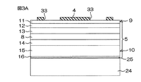
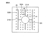
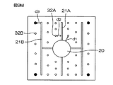
図1は、本発明の一実施形態に係る半導体発光素子1を示す平面図である。図2は、図1のII−II線に沿う断面図である。なお、図1および図2では、明瞭化のため、要素間の比率を一部変更して示している。
この半導体発光素子1は、基板2と、基板2上の金属層3と、金属層3上の絶縁層4と、絶縁層4上の本発明の半導体層の一例としてのIII族窒化物半導体積層構造5と、基板2の裏面(III族窒化物半導体積層構造5と反対側の表面)に接触するように形成されたp側電極6(裏面電極)と、III族窒化物半導体積層構造5の表面に接触するように形成されたn側電極7(表面電極)とを含む。
Hereinafter, embodiments of the present invention will be described in detail with reference to the accompanying drawings.
FIG. 1 is a plan view showing a semiconductor
This semiconductor
基板2は、この実施形態では、シリコン基板で構成されている。むろん、基板2は、たとえば、GaAs(ガリウム砒素)、GaP(リン化ガリウム)等の半導体基板で構成されていてもよい。基板2は、この実施形態では、図1に示すように平面視略正方形状に形成されているが、基板2の平面形状は特に制限されず、たとえば、平面視長方形状であってもよい。また、基板2の厚さは、たとえば、150μm程度であってもよい。
In this embodiment, the
金属層3は、この実施形態では、AuまたはAuを含む合金で構成されている。金属層3は、Au層およびAu合金層それぞれの単層であってもよいし、これらの層および他の金属層が複数積層された層であってもよい。金属層3は、複数の積層構造である場合、たとえば、(III族窒化物半導体積層構造5側)Au/AuBeNi/Au/Mo/Au/Mo/Au/Ti(基板2側)で示される積層構造であってもよい。さらに、金属層3は、金属層3を構成する複数の金属材料間に明瞭な境界が形成されず、当該複数の金属材料が、たとえば基板2側から順々に分布して構成されていてもよい。一方、この実施形態では、金属層3は、後述するように、成長基板24(後述)と基板2との貼り合わせによって第1金属層26(後述)と第2金属層27(後述)とが接合して形成されるものである。したがって、金属層3を構成するAu層の厚さ方向途中に、当該貼り合わせ工程の際に生じる貼合わせ面に起因する境界が存在していてもよい。
In this embodiment, the
金属層3は、基板2の表面全域を覆うように形成されている。また、金属層3の(総)厚さは、たとえば、0.5μm程度であってもよい。
絶縁層4は、たとえば、SiO2膜やSiN膜からなっていてもよい。絶縁層4には、III族窒化物半導体積層構造5の下面を選択的に露出させるコンタクトホール33が形成されており、このコンタクトホール33に、金属層3の一部がコンタクト部32として埋め込まれている。当該コンタクト部32は、III族窒化物半導体積層構造5に接続されている。これにより、半導体発光素子1には、ODR(Omni-Directional-Reflector)構造が形成されている。
The
The insulating
III族窒化物半導体積層構造5は、発光層8と、p型半導体層9と、n型半導体層10とを含む。p型半導体層9は発光層8に対して基板2側に配置されており、n型半導体層10は発光層8に対してn側電極7側に配置されている。こうして、発光層8が、p型半導体層9およびn型半導体層10によって挟持されていて、ダブルヘテロ接合が形成されている。発光層8には、n型半導体層10から電子が注入され、p型半導体層9から正孔が注入される。これらが発光層8で再結合することによって、光が発生するようになっている。
The group III nitride
p型半導体層9は、基板2側から順に、p型GaPコンタクト層11(たとえば0.3μm厚)、p型GaPウィンドウ層12(たとえば1.0μm厚)およびp型AlInPクラッド層13(たとえば0.8μm厚)を積層して構成されている。一方、n型半導体層10は、発光層8の上に、順に、n型AlInPクラッド層14(たとえば0.8μm厚)、n型AlInGaPウィンドウ層15(たとえば1.8μm厚)およびn型GaAsコンタクト層16(たとえば0.3μm厚)を積層して構成されている。
The p-
p型GaPコンタクト層11は、GaPにたとえばp型ドーパントとしてのC(カーボン)を高濃度にドープ(ドーピング濃度は、たとえば、1.8×1019cm−3)することによってp型半導体とされている。一方、n型GaAsコンタクト層16は、GaAsにたとえばn型ドーパントとしてのSiを高濃度にドープ(ドーピング濃度は、たとえば、2.0×1018cm−3)することによってn型半導体層とされている。
The p-type
p型GaPウィンドウ層12は、GaPにたとえばp型ドーパントとしてのMgをドープ(ドーピング濃度は、たとえば、2.1×1018cm−3)することによってp型半導体とされている。一方、n型AlInGaPウィンドウ層15は、AlInGaPにたとえばn型ドーパントとしてのSiをドープ(ドーピング濃度は、たとえば、1.0×1018cm−3)することによってn型半導体層とされている。
The p-type
p型AlInPクラッド層13は、AlInPにたとえばp型ドーパントとしてのMgをドープ(ドーピング濃度は、たとえば、6.0×1016cm−3)することによってp型半導体とされている。一方、n型AlInPクラッド層14は、AlInPにn型ドーパントとしてのSiをドープ(ドーピング濃度は、たとえば、3.0×1017cm−3)することによってn型半導体層とされている。
The p-type
発光層8は、たとえばInGaPを含むMQW(multiple-quantum well)構造(多重量子井戸構造)を有しており、電子と正孔とが再結合することによって光が発生し、その発生した光を増幅させるための層である。
発光層8は、この実施形態では、InGaP層からなる量子井戸層(たとえば5nm厚)とAlInGaP層からなる障壁層(たとえば4nm厚)とを交互に複数周期繰り返し積層して構成された多重量子井戸(MQW:Multiple-Quantum Well)構造を有している。この場合に、InGaPからなる量子井戸層は、Inの組成比が5%以上とされることによって、バンドギャップが比較的小さくなり、AlInGaPからなる障壁層は、バンドギャップが比較的大きくなる。たとえば、量子井戸層(InGaP)と障壁層(AlInGaP)とは交互に2〜7周期繰り返し積層されており、これにより、多重量子井戸構造の発光層8が構成されている。発光波長は、量子井戸層のバンドギャップに対応しており、バンドギャップの調整は、Inの組成比を調整することによって行うことができる。Inの組成比を大きくするほど、バンドギャップが小さくなり、発光波長が大きくなる。この実施形態では、発光波長は、量子井戸層(InGaP層)におけるInの組成を調整することによって、610nm〜630nm(たとえば625nm)とされている。
The
In this embodiment, the light-emitting
図1および図2に示すように、III族窒化物半導体積層構造5は、その一部が除去されることによって、メサ部17を形成している。より具体的には、III族窒化物半導体積層構造5の表面から、n型半導体層10、発光層8およびp型半導体層9の一部がIII族窒化物半導体積層構造5の全周に亘ってエッチング除去され、横断面視略四角形状のメサ部17が形成されている。メサ部17の形状は、断面視略四角形状に限らず、たとえば台形状であってもよい。また、メサ部17は、平面視略四角形状に形成されている。これにより、p型半導体層9のp型GaPウィンドウ層12およびこれよりも基板2側の層が、メサ部17から横方向に引き出された引き出し部18を構成している。図1に示すように、平面視において、メサ部17は引き出し部18に取り囲まれている。
As shown in FIGS. 1 and 2, the group III nitride
メサ部17の表面には、この実施形態では、微細な凹凸形状19が形成されている。この微細な凹凸形状19によって、III族窒化物半導体積層構造5から取り出される光を拡散させることができる。この実施形態では、後述するようにn型GaAsコンタクト層16がn側電極7の形状に合わせて選択的に除去されることによってn型AlInGaPウィンドウ層15が露出しており、この露出面に微細な凹凸形状19が形成されている。なお、図1では、明瞭化のため微細な凹凸形状19を省略している。
In this embodiment, a fine
裏面電極としてのp側電極6は、この実施形態では、AuまたはAuを含む合金で構成されている。具体的には、(基板2側)Ti/Au/Mo/Auで示される積層構造であってもよい。また、p側電極6は、基板2の裏面全域を覆うように形成されている。
表面電極としてのn側電極7は、この実施形態では、AuまたはAuを含む合金で構成されている。具体的には、(III族窒化物半導体積層構造5側)Au/Ge/Ni/Auで示される積層構造であってもよい。
In this embodiment, the p-
In this embodiment, the n-
また、n側電極7は、パッド電極部20と、当該パッド電極部20の周囲に一定の領域を区画するようにパッド電極部20から選択的に枝状に延びる枝状電極部21とを一体的に含む。
この実施形態では、平面視において、パッド電極部20がメサ部17の略中央に配置されており、当該パッド電極部20とメサ部17の4つの隅のそれぞれとの間に包囲領域22A,22B,22C,22Dを区画するように枝状電極部21が形成されている。各包囲領域22A〜22Dは、パッド電極部20からメサ部17の各周縁(もしくは端面)に向かって十字状に延びる枝状電極部21の中間部21Aと、当該十字型の中間部21Aに交差してメサ部17の互いに対向する一対の周縁(もしくは端面)に沿って延びる枝状電極部の外周部21Bと、パッド電極部20によって取り囲まれている。一方、包囲領域22A〜22Dを除く外周部21Bの外側の領域は、メサ部17の外周領域23となっている。
The n-
In this embodiment, the
そして、この実施形態では、n型GaAsコンタクト層16がn側電極7と同じ形状を有していることから、包囲領域22A〜22Dおよび外周領域23にn型AlInGaPウィンドウ層15が露出している。
金属層3のコンタクト部32は、図1に示すように、基板2の面内に離散的に配列されている。たとえば、平面視四角形状のメサ部17内に行列状に配列されていてもよい。
In this embodiment, since the n-type
The
この実施形態では、一対の外周部21Bの外側の各外周領域23に、複数のコンタクト部32からなる外側列321が一列ずつ設けられている。各外側列321において、コンタクト部32は、外周部21Bとの間に等しい間隔を保って外周部21Bに沿って配列されている。
一方、一対の外周部21Bの内側の包囲領域22A〜22Dには、複数のコンタクト部32からなる内側列322が設けられている。内側列322は、たとえば、外側列321と平行に複数列設けられている。この実施形態では、包囲領域22Aと包囲領域22Dとの間を跨るように二列形成され、包囲領域22Bと包囲領域22Cとの間を跨るように二列形成されている。
In this embodiment, an
On the other hand, in the surrounding
次に、複数のコンタクト部32について以下の説明を加える。
各コンタクト部32の径は、たとえば、8μm〜15μmである。また、複数のコンタクト部32の総数は、たとえば、28個〜60個である。この実施形態では、44個のコンタクト部32が形成されている。また、半導体発光素子1の発光面積(この実施形態では、メサ部17の表面面積)に対する複数のコンタクト部32の総面積(各コンタクト部32の径×個数)で示される被覆率(コンタクト部32面積/発光面積)は、たとえば、6%〜40%である。
Next, the following description will be added to the plurality of
The diameter of each
また、次に示す距離d1,d2およびd3に関して、d1>d2>d3を満たしている。
d1:内側列322のコンタクト部32のうち、パッド電極部20の周囲の本発明の第1コンタクト部の一例としてのコンタクト部32A(図1の破線で囲まれた領域R内のコンタクト部32)とパッド電極部20との距離
d2:コンタクト部32Aと中間部21Aとの距離
d3:外側列321の本発明の第2コンタクト部の一例としてのコンタクト部32Bと外周部21Bとの距離
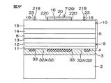
図3A〜図3Iは、図1および図2の半導体発光素子1の製造工程を工程順に示す図である。
Further, the following distances d 1 , d 2 and d 3 satisfy d 1 > d 2 > d 3 .
d 1 : of the
半導体発光素子1を製造するには、たとえば図3Aに示すように、GaAs等からなる成長基板24上に、エピタキシャル成長によってIII族窒化物半導体積層構造5が形成される。成長方法は、たとえば、分子線エピタキシャル成長法、有機金属気相成長法等、公知の成長方法を適用できる。この段階では、III族窒化物半導体積層構造5は、成長基板24の側から順に、n型AlInGaPエッチングストップ層25、n型GaAsコンタクト層16、n型AlInGaPウィンドウ層15、n型AlInPクラッド層14、発光層8、p型AlInPクラッド層13、p型GaPウィンドウ層12およびp型GaPコンタクト層11を含んでいる。III族窒化物半導体積層構造5の形成後、たとえばCVD法によって、絶縁層4が形成される。
To manufacture the semiconductor
次に、図3Bに示すように、たとえば蒸着法によって、絶縁層4上に第1金属層26(たとえば1.7μm厚)が形成される。第1金属層26は、AuまたはAuを含む合金で構成されており、少なくとも最表面がAu層で構成されている。第1金属層26の一部はコンタクト部32としてコンタクトホール33に入り込み、p型GaPコンタクト層11に接続される。
Next, as shown in FIG. 3B, a first metal layer 26 (for example, having a thickness of 1.7 μm) is formed on insulating
次の工程は、成長基板24と基板2との貼合わせ工程である。貼合わせ工程では、成長基板24上の第1金属層26と基板2上の第2金属層27とが接合される。第2金属層27は、AuまたはAuを含む合金で構成されており、少なくとも最表面がAu層で構成されている。この第2金属層27は、貼合わせ前に、たとえば蒸着法によって、基板2の表面(前述のp側電極6が形成される面の反対面)に形成されたものである。
The next step is a step of bonding the
より具体的には、図3Cに示すように、第1および第2金属層26,27同士を向い合せた状態で成長基板24と基板2とを重ね合わせ、第1および第2金属層26,27を接合する。第1および第2金属層26,27の接合は、たとえば熱圧着によって行ってもよい。熱圧着の条件は、たとえば、温度が250℃〜700℃、好ましくは約300℃〜400℃であり、圧力が10MPa〜20MPaであってもよい。この接合によって、図3Dに示すように、第1および第2金属層26,27が合わさって金属層3が形成される。
More specifically, as shown in FIG. 3C, the
次に、図3Dに示すように、たとえばウエットエッチングによって、成長基板24が除去される。ここで、III族窒化物半導体積層構造5の最表面にn型AlInGaPエッチングストップ層25が形成されていることから、当該ウエットエッチングの際に、半導体発光素子1の特性に寄与するn型GaAsコンタクト層16やn型AlInGaPウィンドウ層15等に影響を与えなくて済む。その後、n型AlInGaPエッチングストップ層25も除去される。
Next, as shown in FIG. 3D, the
次の工程は、n側電極7の形成工程である。この実施形態では、リフトオフ法によってn側電極7が形成される。より具体的には、図3Eに示すように、まず、n側電極7の電極パターンと同一パターンの開口を有するレジスト28が、n型GaAsコンタクト層16上に形成される。次に、たとえば蒸着法によって、III族窒化物半導体積層構造5上に電極材料膜29が積層される。
The next step is a step of forming the n-
次に、図3Fに示すように、レジスト28上の電極材料膜29が、レジスト28と共に除去される。これにより、n型GaAsコンタクト層16上に残った電極材料膜29からなるn側電極7が形成される。その後、n側電極7から露出するn型GaAsコンタクト層16がエッチングによって除去される。これにより、n側電極7以外の部分にn型AlInGaPウィンドウ層15が露出することになる。
Next, as shown in FIG. 3F, the
次に、図3Gに示すように、たとえばフロスト処理(ウエットエッチング)等によって、n型AlInGaPウィンドウ層15の表面に微細な凹凸形状19が形成される。なお、フロスト処理は、ドライエッチングによって行ってもよい。
次に、図3Hに示すように、III族窒化物半導体積層構造5の周縁部が選択的に除去されることによって、メサ部17および引き出し部18が形成される。メサ部17および引き出し部18の形成は、たとえば、ウエットエッチングによって行ってもよい。
Next, as shown in FIG. 3G,
Next, as shown in FIG. 3H, the
次に、図3Iに示すように、たとえば蒸着法によって、基板2の裏面にp側電極6が形成される。以上の工程を経て、半導体発光素子1が得られる。
以上、この半導体発光素子1によれば、図1に示すように、枝状電極部21の外周部21Bと、これに隣接する外側列321のコンタクト部32Bとの距離d3が最も小さくされている。当該外周部21Bはパッド電極部20から最も離れているので、パッド電極部20やパッド電極部20に直接接続された中間部21Aに比べて比較的電流が流れにくい。しかしながら、上記のように距離d3を小さくすることで、コンタクト部32Bにも良好に電流を流すことができる。一方、パッド電極部20の周囲においても、距離d1>距離d2とし、コンタクト部32Aをパッド電極部20よりも枝状電極部21の中間部21Aに近づけることで、電流をパッド電極部20に集中させず、パッド電極部20の周囲の枝状電極部21(中間部21A)にも分散させることができる。これにより、基板2の面内のほぼ全体に亘って離散的に配置された複数のコンタクト部32を有効に利用できるので、低い順方向電圧(VF)でも複数のコンタクト部32に万遍なく電流を流すことができる。その結果、低い順方向電圧(VF)で高輝度な半導体発光素子1を提供することができる。
Next, as shown in FIG. 3I, a p-
As described above, according to the semiconductor
以上、本発明の実施形態を説明したが、本発明は、他の形態で実施することもできる。
たとえば、n側電極7のパターンおよびコンタクト部32の配列パターンは、図1に示した例に限らず、図4〜図8に示すものであってもよい。なお、図4以降の図では、距離d1,d2およびd3に関して、d1>d2>d3を満たすように図示されていない場合がある。
The embodiments of the present invention have been described above, but the present invention can be embodied in other forms.
For example, the pattern of the n-
たとえば、図4〜図6に示すように、枝状電極部21の外周部21Bは、中央のパッド電極部20から各周縁(もしくは端面)に向かって四方に延びる枝状電極部21の中間部21Aのそれぞれに接続され、メサ部17の各周縁(もしくは端面)に沿って形成されていてもよい。この場合、図4および図5に示すように、中央のパッド電極部20に対して、4本の略T字状の枝状電極部21(中間部21A+外周部21B)が接続されていてもよいし、図6に示すように、枝状電極部21が、中央のパッド電極部20から各周縁(もしくは端面)に向かって四方に延び、さらに屈曲してメサ部17の各周縁(もしくは端面)に延びることによって、全体として卍状に形成されていてもよい。
For example, as shown in FIG. 4 to FIG. 6, an outer
上記の場合、複数のコンタクト部32は、外周領域23に形成されておらず、包囲領域22A〜22Dに形成された内側列322のみで構成されていてもよい。むろん、外周領域23に形成されていても問題はない。
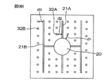
また、図7および図8に示すように、半導体発光素子1は、メサ部17の一つの角部に配置されたパッド電極部30と、当該パッド電極部30からメサ部17の周縁(もしくは端面)に沿って形成された枝状電極部31とを備えていてもよい。枝状電極部31は、メサ部17の周縁の全周に亘って形成された外周部31Aを含んでいてもよい。この外周部31Aで取り囲まれた内側に包囲領域34が区画され、外周部31Aの外側が外周領域35であってもよい。さらに、枝状電極部31は、図8に示すように、包囲領域34を複数の包囲領域34A,34B,34Cに分割する架設部31Bを含んでいてもよい。
In the above case, the plurality of
As shown in FIGS. 7 and 8, the semiconductor
この実施形態では、外周部31Aは、メサ部17の周縁に沿う4辺からなる平面視四角形状に形成されており、パッド電極部30に直接接続された第1部分311Aおよびパッド電極部30の対角から延びる第2部分312Aをさらに含んでいる。この場合、本発明の第2コンタクト部の一例としてのコンタクト部32Bは、たとえば、第2部分312Aに沿って配列されたコンタクト部32であってもよい。なお、図7および図8では、コンタクト部32A,32Bは、包囲領域34のみに形成されているが、外周領域35に形成されていてもよい。
In this embodiment, the outer
その他、特許請求の範囲に記載された事項の範囲で種々の設計変更を施すことが可能である。 In addition, various design changes can be made within the scope of the matters described in the claims.
次に、本発明を実施例に基づいて説明するが、本発明は下記の実施例によって限定されるものではない。
(1)輝度(IV)および順方向電圧(VF)の測定
図9A〜図9Qおよび表1,2に示す条件で半導体発光素子を作製し、それぞれについて、輝度(IV)および順方向電圧(VF)を測定した。結果を図10および図11に示す。図10、図11および表1,2に示すように、d1>d2>d3を満たすAパターンが、低い順方向電圧(VF)でかつ高輝度を達成している。
Next, the present invention will be described based on examples, but the present invention is not limited to the following examples.
(1) Measurement of Luminance (IV) and Forward Voltage (VF) Semiconductor light-emitting devices were manufactured under the conditions shown in FIGS. 9A to 9Q and Tables 1 and 2, and for each, the luminance (IV) and forward voltage (VF) were measured. ) Was measured. The results are shown in FIGS. As shown in FIGS. 10 and 11 and Tables 1 and 2, the pattern A that satisfies d 1 > d 2 > d 3 achieves a low forward voltage (VF) and high luminance.

(2)枝状電極部の有無による評価
図12に示す4パターンの半導体発光素子を作製した。それぞれについて、前述のメサ部17の表面にフロスト処理によって微細な凹凸形状19が形成されたものと、形成しなかったものを用意し、評価サンプルを合計8パターンとした。図12において、右側のパターンは、それぞれ、上側から前述の図4のパターンおよび図5のパターンと同一である。そして、各評価サンプルについて、輝度(IV)および順方向電圧(VF)を測定した。結果を図13および図14に示す。図13および図14に示すように、枝有り(枝状電極部21有り)のパターンであれば、枝無しのパターンに比べて、低い順方向電圧(VF)で同等の輝度(IV)を達成している。これにより、離散的に配列されたODR構造(コンタクト部32)を縫うように枝状電極部21を形成した方が、低い順方向電圧(VF)を実現できることが分かった。
(2) Evaluation Based on Presence or Absence of Branched Electrode Section Four patterns of semiconductor light emitting devices shown in FIG. 12 were produced. In each case, a sample in which
1 :半導体発光素子
2 基板
3 金属層
4 絶縁層
5 III族窒化物半導体積層構造
6 p側電極
7 n側電極
8 発光層
9 p型半導体層
10 n型半導体層
19 微細な凹凸形状
20 パッド電極部
21 枝状電極部
21A 中間部
21B 外周部
30 パッド電極部
31 枝状電極部
31A 外周部
31B 架設部
32 コンタクト部
311A 第1部分
312A 第2部分
Reference Signs List 1: semiconductor light-emitting
Claims (15)
前記基板上の金属層と、
前記金属層上に形成され、発光層、前記発光層に対して前記基板側に配置された第1導電型層、および前記発光層に対して前記基板の反対側に配置された第2導電型層を含む半導体層と、
前記金属層と前記第1導電型層とを電気的に接続しており、前記基板の法線方向から見た平面視において前記基板の面内のほぼ全体に亘って離散的に配置された複数のコンタクト部と、
前記半導体層上に形成され、パッド電極部と、平面視において当該パッド電極部から前記複数のコンタクト部の間を縫って枝状に延びる枝状電極部とを含む表面電極と、
前記基板の裏面上の裏面電極とを含み、
前記半導体層は、前記第2導電型層、前記発光層および前記第1導電型層の一部が除去されることによって形成された平面視略四角形状のメサ部と、前記メサ部を形成する前記第1導電型層の前記一部よりも前記基板側の前記第1導電型層の残りの部分によって形成され、前記メサ部を取り囲む引き出し部とを含み、
前記枝状電極部は、前記パッド電極部から前記メサ部の4つの端面に向かって十字状に延びる中間部と、前記十字型の中間部に交差して前記メサ部の互いに対向する一対の端面に沿って延びる外周部とを含み、
前記半導体層上の領域は、平面視において、前記パッド電極部、前記枝状電極部の前記中間部および前記枝状電極部の前記外周部に取り囲まれた包囲領域と、前記枝状電極部の前記外周部の外側の外周領域とに区画され、
前記コンタクト部は、前記外周領域において前記枝状電極部の前記外周部に沿って配列された外側列と、前記包囲領域に設けられ、前記外側列と平行に配列された内側列とを含み、
前記内側列の前記コンタクト部のうち前記パッド電極部の周囲の第1コンタクト部と前記パッド電極部との平面視における距離d1と、当該第1コンタクト部とこの第1コンタクト部に最も近い前記枝状電極部の前記中間部との平面視における距離d2と、前記コンタクト部のうち前記外側列としての第2コンタクト部とこの第2コンタクト部に最も近い前記枝状電極部の前記外周部との平面視における距離d3との関係が、d1>d2>d3を満たす、半導体発光素子。 Board and
A metal layer on the substrate,
A light emitting layer formed on the metal layer, a first conductive type layer disposed on the substrate side with respect to the light emitting layer, and a second conductive type disposed on the opposite side of the substrate with respect to the light emitting layer A semiconductor layer including a layer;
The metal layer and the first conductivity type layer are electrically connected to each other, and are disposed discretely over substantially the entire surface of the substrate in a plan view as viewed from a normal direction of the substrate. Contact part,
A surface electrode formed on the semiconductor layer and including a pad electrode portion and a branch electrode portion extending in a branch shape by sewing between the plurality of contact portions from the pad electrode portion in plan view;
A back electrode on the back of the substrate,
The semiconductor layer forms a mesa portion having a substantially square shape in plan view formed by removing a part of the second conductivity type layer, the light emitting layer, and the first conductivity type layer, and the mesa portion. A lead portion formed by the remaining portion of the first conductivity type layer closer to the substrate than the part of the first conductivity type layer and surrounding the mesa portion;
The branch-like electrode portion includes a middle portion extending in a cross shape from the pad electrode portion toward four end surfaces of the mesa portion, and a pair of end faces of the mesa portion crossing the cross-shaped middle portion and facing each other. And an outer peripheral portion extending along
The region on the semiconductor layer is, in plan view, the pad electrode portion, the surrounding region surrounded by the intermediate portion of the branch electrode portion and the outer peripheral portion of the branch electrode portion, and the surrounding region of the branch electrode portion. Partitioned into an outer peripheral region outside the outer peripheral portion,
The contact portion includes an outer row arranged along the outer peripheral portion of the branch electrode portion in the outer peripheral region, and an inner row provided in the surrounding region and arranged in parallel with the outer row,
The distance d 1 in plan view of the first contact portion of the periphery of the pad electrode portion of the contact portion of the inner row and the pad electrode portion closest said to the first contact portion and the first contact portion the distance d 2 in plan view of the intermediate portion of the branch electrode portion, the outer circumferential portion closest the branch electrode portion to the second contact portion and second contact portion as the outer row of the contact portion relationship between the distance d 3 in plan view with satisfies the d 1> d 2> d 3 , the semiconductor light emitting element.
前記コンタクト部は、前記金属層の一部からなり、前記絶縁層を貫通して前記第1導電型層に接続されている、請求項1に記載の半導体発光素子。 Including an insulating layer between the semiconductor layer and the metal layer,
2. The semiconductor light emitting device according to claim 1, wherein the contact portion is formed of a part of the metal layer, and penetrates the insulating layer and is connected to the first conductivity type layer. 3.
前記第2導電型層の前記表面は、前記第2導電型層の前記側面よりも粗い面である、請求項1〜9のいずれか一項に記載の半導体発光素子。 The second conductivity type layer has a surface and side surfaces exposed from the surface electrode in plan view,
Wherein the surface of the second conductivity type layer is a rough surface than the side surface of the second conductivity type layer, the semiconductor light-emitting device according to any one of claims 1 to 9.
前記第2導電型層の前記第2層は、前記表面電極と同じ形状を有している、請求項10または11に記載の半導体発光素子。 The second conductivity type layer is formed on the surface of the second conductivity type layer, the first layer including the surface and the side surface exposed from the surface electrode in plan view, and the second layer covered by the surface electrode. And two layers,
The semiconductor light emitting device according to claim 10 , wherein the second layer of the second conductivity type has the same shape as the surface electrode.
Priority Applications (2)
| Application Number | Priority Date | Filing Date | Title |
|---|---|---|---|
| JP2015194619A JP6650143B2 (en) | 2015-09-30 | 2015-09-30 | Semiconductor light emitting device |
| US15/277,518 US10707392B2 (en) | 2015-09-30 | 2016-09-27 | Semiconductor light-emitting element |
Applications Claiming Priority (1)
| Application Number | Priority Date | Filing Date | Title |
|---|---|---|---|
| JP2015194619A JP6650143B2 (en) | 2015-09-30 | 2015-09-30 | Semiconductor light emitting device |
Publications (3)
| Publication Number | Publication Date |
|---|---|
| JP2017069437A JP2017069437A (en) | 2017-04-06 |
| JP2017069437A5 JP2017069437A5 (en) | 2018-09-13 |
| JP6650143B2 true JP6650143B2 (en) | 2020-02-19 |
Family
ID=58409909
Family Applications (1)
| Application Number | Title | Priority Date | Filing Date |
|---|---|---|---|
| JP2015194619A Active JP6650143B2 (en) | 2015-09-30 | 2015-09-30 | Semiconductor light emitting device |
Country Status (2)
| Country | Link |
|---|---|
| US (1) | US10707392B2 (en) |
| JP (1) | JP6650143B2 (en) |
Families Citing this family (2)
| Publication number | Priority date | Publication date | Assignee | Title |
|---|---|---|---|---|
| JP6916062B2 (en) * | 2017-08-22 | 2021-08-11 | ローム株式会社 | Semiconductor light emitting device and manufacturing method of semiconductor light emitting device |
| CN111384216A (en) * | 2020-02-27 | 2020-07-07 | 扬州乾照光电有限公司 | LED chip and manufacturing method thereof |
Family Cites Families (11)
| Publication number | Priority date | Publication date | Assignee | Title |
|---|---|---|---|---|
| JPH0538921U (en) * | 1991-10-23 | 1993-05-25 | 三菱電線工業株式会社 | Electrode structure of light emitting element |
| JP2007221029A (en) * | 2006-02-20 | 2007-08-30 | Sony Corp | Semiconductor light emitting element and its manufacturing method |
| JP2008288248A (en) * | 2007-05-15 | 2008-11-27 | Hitachi Cable Ltd | Semiconductor light-emitting element |
| JP4985260B2 (en) * | 2007-09-18 | 2012-07-25 | 日立電線株式会社 | Light emitting device |
| US7915629B2 (en) * | 2008-12-08 | 2011-03-29 | Cree, Inc. | Composite high reflectivity layer |
| JP4871967B2 (en) * | 2009-02-10 | 2012-02-08 | Dowaエレクトロニクス株式会社 | Semiconductor light emitting device and manufacturing method thereof |
| JP2010278112A (en) * | 2009-05-27 | 2010-12-09 | Hitachi Cable Ltd | Semiconductor light emitting element |
| US9006774B2 (en) * | 2010-02-09 | 2015-04-14 | Epistar Corporation | Optoelectronic device and the manufacturing method thereof |
| TWI762930B (en) * | 2010-02-09 | 2022-05-01 | 晶元光電股份有限公司 | Optoelectronic device |
| TWI577045B (en) * | 2013-07-10 | 2017-04-01 | 晶元光電股份有限公司 | Light-emitting element |
| JP6423234B2 (en) * | 2013-11-21 | 2018-11-14 | ローム株式会社 | Semiconductor light emitting device and manufacturing method thereof |
-
2015
- 2015-09-30 JP JP2015194619A patent/JP6650143B2/en active Active
-
2016
- 2016-09-27 US US15/277,518 patent/US10707392B2/en active Active
Also Published As
| Publication number | Publication date |
|---|---|
| US20170092828A1 (en) | 2017-03-30 |
| JP2017069437A (en) | 2017-04-06 |
| US10707392B2 (en) | 2020-07-07 |
Similar Documents
| Publication | Publication Date | Title |
|---|---|---|
| JP5256101B2 (en) | Semiconductor light emitting device | |
| JP5959627B2 (en) | Electrical series connection of light-emitting nanowires | |
| JP2017028287A (en) | Light-emitting device and method for manufacturing the same | |
| KR20130031254A (en) | Optoelectronic semiconductor chip | |
| JP6694650B2 (en) | Semiconductor light emitting element | |
| US20120299048A1 (en) | Semiconductor light emitting device having current blocking layer | |
| KR20160016361A (en) | Light emitting diode and method of fabricating the same | |
| KR20140049877A (en) | Semiconductor light emitting diode with improved current spreading performance and high brightness comprising trench isolating light emitting region | |
| KR102540321B1 (en) | Semiconductor light emitting diode | |
| JP3706458B2 (en) | Semiconductor light emitting device | |
| US10164154B2 (en) | Semiconductor light emitting device | |
| WO2017206772A1 (en) | Light emitting diode with electrostatic protection function and manufacturing method therefor | |
| JP6650143B2 (en) | Semiconductor light emitting device | |
| JP2014022401A (en) | Nitride semiconductor light-emitting element | |
| TWI230470B (en) | Light-emitting diode array | |
| JP6204131B2 (en) | Light emitting device and manufacturing method thereof | |
| TW201401558A (en) | Light emitting diode structure and manufacturing method thereof | |
| KR20130111792A (en) | Nitride based light emitting diode with improved current spreading performance and high brightness | |
| JP2006237467A (en) | Semiconductor light emitting element and manufacturing method thereof | |
| US20150333228A1 (en) | High-brightness semiconductor light-emitting device having excellent current dispersion effect by including separation region | |
| JP3691207B2 (en) | Semiconductor light emitting device | |
| KR20120090493A (en) | Light emitting diode assembly and method of manufacturing the same | |
| JP6190591B2 (en) | Semiconductor light emitting device | |
| JP5772213B2 (en) | Light emitting element | |
| CN206271745U (en) | Semiconductor light-emitting elements |
Legal Events
| Date | Code | Title | Description |
|---|---|---|---|
| A521 | Request for written amendment filed |
Free format text: JAPANESE INTERMEDIATE CODE: A523 Effective date: 20180801 |
|
| A621 | Written request for application examination |
Free format text: JAPANESE INTERMEDIATE CODE: A621 Effective date: 20180918 |
|
| A131 | Notification of reasons for refusal |
Free format text: JAPANESE INTERMEDIATE CODE: A131 Effective date: 20190620 |
|
| A977 | Report on retrieval |
Free format text: JAPANESE INTERMEDIATE CODE: A971007 Effective date: 20190619 |
|
| A521 | Request for written amendment filed |
Free format text: JAPANESE INTERMEDIATE CODE: A523 Effective date: 20190807 |
|
| TRDD | Decision of grant or rejection written | ||
| A01 | Written decision to grant a patent or to grant a registration (utility model) |
Free format text: JAPANESE INTERMEDIATE CODE: A01 Effective date: 20191219 |
|
| A61 | First payment of annual fees (during grant procedure) |
Free format text: JAPANESE INTERMEDIATE CODE: A61 Effective date: 20200114 |
|
| R150 | Certificate of patent or registration of utility model |
Ref document number: 6650143 Country of ref document: JP Free format text: JAPANESE INTERMEDIATE CODE: R150 |
|
| R250 | Receipt of annual fees |
Free format text: JAPANESE INTERMEDIATE CODE: R250 |
|
| R250 | Receipt of annual fees |
Free format text: JAPANESE INTERMEDIATE CODE: R250 |