JP6649773B2 - 発光構造及びマウント - Google Patents
発光構造及びマウント Download PDFInfo
- Publication number
- JP6649773B2 JP6649773B2 JP2015562452A JP2015562452A JP6649773B2 JP 6649773 B2 JP6649773 B2 JP 6649773B2 JP 2015562452 A JP2015562452 A JP 2015562452A JP 2015562452 A JP2015562452 A JP 2015562452A JP 6649773 B2 JP6649773 B2 JP 6649773B2
- Authority
- JP
- Japan
- Prior art keywords
- light emitting
- led
- contact
- orientation
- mount
- Prior art date
- Legal status (The legal status is an assumption and is not a legal conclusion. Google has not performed a legal analysis and makes no representation as to the accuracy of the status listed.)
- Active
Links
- 238000000034 method Methods 0.000 claims description 10
- 239000012212 insulator Substances 0.000 claims description 2
- 238000004519 manufacturing process Methods 0.000 claims description 2
- 229910052751 metal Inorganic materials 0.000 description 32
- 239000002184 metal Substances 0.000 description 32
- 239000004065 semiconductor Substances 0.000 description 15
- 239000000758 substrate Substances 0.000 description 15
- 239000000463 material Substances 0.000 description 8
- 239000002019 doping agent Substances 0.000 description 3
- 239000000203 mixture Substances 0.000 description 3
- 229910052594 sapphire Inorganic materials 0.000 description 3
- 239000010980 sapphire Substances 0.000 description 3
- IJGRMHOSHXDMSA-UHFFFAOYSA-N Atomic nitrogen Chemical compound N#N IJGRMHOSHXDMSA-UHFFFAOYSA-N 0.000 description 2
- 238000010586 diagram Methods 0.000 description 2
- 238000005530 etching Methods 0.000 description 2
- 230000005496 eutectics Effects 0.000 description 2
- -1 for example Substances 0.000 description 2
- HBMJWWWQQXIZIP-UHFFFAOYSA-N silicon carbide Chemical compound [Si+]#[C-] HBMJWWWQQXIZIP-UHFFFAOYSA-N 0.000 description 2
- 229910010271 silicon carbide Inorganic materials 0.000 description 2
- 229910000679 solder Inorganic materials 0.000 description 2
- 238000005476 soldering Methods 0.000 description 2
- GYHNNYVSQQEPJS-UHFFFAOYSA-N Gallium Chemical compound [Ga] GYHNNYVSQQEPJS-UHFFFAOYSA-N 0.000 description 1
- 229910052782 aluminium Inorganic materials 0.000 description 1
- XAGFODPZIPBFFR-UHFFFAOYSA-N aluminium Chemical compound [Al] XAGFODPZIPBFFR-UHFFFAOYSA-N 0.000 description 1
- 230000004888 barrier function Effects 0.000 description 1
- 239000000919 ceramic Substances 0.000 description 1
- 238000005229 chemical vapour deposition Methods 0.000 description 1
- 239000002131 composite material Substances 0.000 description 1
- 238000005520 cutting process Methods 0.000 description 1
- 229910052733 gallium Inorganic materials 0.000 description 1
- 239000011521 glass Substances 0.000 description 1
- 230000012447 hatching Effects 0.000 description 1
- 229910052738 indium Inorganic materials 0.000 description 1
- APFVFJFRJDLVQX-UHFFFAOYSA-N indium atom Chemical compound [In] APFVFJFRJDLVQX-UHFFFAOYSA-N 0.000 description 1
- 239000011810 insulating material Substances 0.000 description 1
- 238000005468 ion implantation Methods 0.000 description 1
- 229910003465 moissanite Inorganic materials 0.000 description 1
- 238000001451 molecular beam epitaxy Methods 0.000 description 1
- 229910052757 nitrogen Inorganic materials 0.000 description 1
- 230000006911 nucleation Effects 0.000 description 1
- 238000010899 nucleation Methods 0.000 description 1
- 230000003287 optical effect Effects 0.000 description 1
- 238000002360 preparation method Methods 0.000 description 1
- 229910002059 quaternary alloy Inorganic materials 0.000 description 1
- 239000010703 silicon Substances 0.000 description 1
- 229910052710 silicon Inorganic materials 0.000 description 1
- 229910002058 ternary alloy Inorganic materials 0.000 description 1
- 238000001429 visible spectrum Methods 0.000 description 1
Images


Classifications
-
- H—ELECTRICITY
- H01—ELECTRIC ELEMENTS
- H01L—SEMICONDUCTOR DEVICES NOT COVERED BY CLASS H10
- H01L27/00—Devices consisting of a plurality of semiconductor or other solid-state components formed in or on a common substrate
- H01L27/15—Devices consisting of a plurality of semiconductor or other solid-state components formed in or on a common substrate including semiconductor components having potential barriers, specially adapted for light emission
- H01L27/153—Devices consisting of a plurality of semiconductor or other solid-state components formed in or on a common substrate including semiconductor components having potential barriers, specially adapted for light emission in a repetitive configuration, e.g. LED bars
- H01L27/156—Devices consisting of a plurality of semiconductor or other solid-state components formed in or on a common substrate including semiconductor components having potential barriers, specially adapted for light emission in a repetitive configuration, e.g. LED bars two-dimensional arrays
-
- H—ELECTRICITY
- H01—ELECTRIC ELEMENTS
- H01L—SEMICONDUCTOR DEVICES NOT COVERED BY CLASS H10
- H01L33/00—Semiconductor devices having potential barriers specially adapted for light emission; Processes or apparatus specially adapted for the manufacture or treatment thereof or of parts thereof; Details thereof
- H01L33/005—Processes
-
- H—ELECTRICITY
- H01—ELECTRIC ELEMENTS
- H01L—SEMICONDUCTOR DEVICES NOT COVERED BY CLASS H10
- H01L33/00—Semiconductor devices having potential barriers specially adapted for light emission; Processes or apparatus specially adapted for the manufacture or treatment thereof or of parts thereof; Details thereof
- H01L33/36—Semiconductor devices having potential barriers specially adapted for light emission; Processes or apparatus specially adapted for the manufacture or treatment thereof or of parts thereof; Details thereof characterised by the electrodes
- H01L33/38—Semiconductor devices having potential barriers specially adapted for light emission; Processes or apparatus specially adapted for the manufacture or treatment thereof or of parts thereof; Details thereof characterised by the electrodes with a particular shape
-
- H—ELECTRICITY
- H01—ELECTRIC ELEMENTS
- H01L—SEMICONDUCTOR DEVICES NOT COVERED BY CLASS H10
- H01L33/00—Semiconductor devices having potential barriers specially adapted for light emission; Processes or apparatus specially adapted for the manufacture or treatment thereof or of parts thereof; Details thereof
- H01L33/48—Semiconductor devices having potential barriers specially adapted for light emission; Processes or apparatus specially adapted for the manufacture or treatment thereof or of parts thereof; Details thereof characterised by the semiconductor body packages
- H01L33/62—Arrangements for conducting electric current to or from the semiconductor body, e.g. lead-frames, wire-bonds or solder balls
-
- H—ELECTRICITY
- H01—ELECTRIC ELEMENTS
- H01L—SEMICONDUCTOR DEVICES NOT COVERED BY CLASS H10
- H01L2924/00—Indexing scheme for arrangements or methods for connecting or disconnecting semiconductor or solid-state bodies as covered by H01L24/00
- H01L2924/0001—Technical content checked by a classifier
- H01L2924/0002—Not covered by any one of groups H01L24/00, H01L24/00 and H01L2224/00
-
- H—ELECTRICITY
- H01—ELECTRIC ELEMENTS
- H01L—SEMICONDUCTOR DEVICES NOT COVERED BY CLASS H10
- H01L2933/00—Details relating to devices covered by the group H01L33/00 but not provided for in its subgroups
- H01L2933/0008—Processes
- H01L2933/0033—Processes relating to semiconductor body packages
-
- H—ELECTRICITY
- H01—ELECTRIC ELEMENTS
- H01L—SEMICONDUCTOR DEVICES NOT COVERED BY CLASS H10
- H01L2933/00—Details relating to devices covered by the group H01L33/00 but not provided for in its subgroups
- H01L2933/0008—Processes
- H01L2933/0033—Processes relating to semiconductor body packages
- H01L2933/0066—Processes relating to semiconductor body packages relating to arrangements for conducting electric current to or from the semiconductor body
Landscapes
- Engineering & Computer Science (AREA)
- Microelectronics & Electronic Packaging (AREA)
- Power Engineering (AREA)
- Computer Hardware Design (AREA)
- Manufacturing & Machinery (AREA)
- Physics & Mathematics (AREA)
- Condensed Matter Physics & Semiconductors (AREA)
- General Physics & Mathematics (AREA)
- Led Device Packages (AREA)
- Led Devices (AREA)
Description
Claims (8)
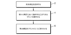
- 発光デバイスを製造する方法であって、
複数の発光ダイオード(LED)を含む発光構造を提供することであって、前記複数のLEDの各々はpコンタクト及びnコンタクトを含む、ことと、
マウントを提供することであって、前記マウントはアノードパッド及びカソードパッドを含む、ことと、
少なくとも1つのpコンタクトを前記アノードパッドのうち少なくとも1つに、及び、少なくとも1つのnコンタクトを前記カソードパッドのうち少なくとも1つに、第1の向き又は第2の向きにおいて整合させることと、
前記マウントに前記発光構造を取り付けることと、
前記第1の向きにおいて前記複数のLEDにおける前記マウント上の第1の電気的接続を、及び、前記第2の向きにおいて前記複数のLEDにおける前記マウント上の第2の電気的接続を提供することと、
前記第1の向きにおいて前記第1の電気的接続に第1の電圧を供給することと、
前記第2の向きにおいて前記第2の電気的接続に、前記第1の電圧と異なる第2の電圧を供給することと、
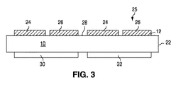
を含む方法。 - 発光構造であって、
複数の発光ダイオード(LED)であり、各LEDはn型領域とp型領域との間に配設される発光層を含む、複数のLEDと、
前記p型領域上に配設されるpコンタクトと、
前記n型領域上に配設されるnコンタクトと、
を含む、発光構造と、
アノードパッド及びカソードパッドを含むマウントと、
を含み、
前記nコンタクト及び前記pコンタクトは、前記アノードパッドのうち少なくとも1つ及び前記カソードパッドのうち少なくとも1つの上に第1の向きにおいて、又は前記アノードパッドのうち少なくとも1つ及び前記カソードパッドのうち少なくとも1つの上に第2の向きにおいてのいずれかで前記マウントに付けられ、
前記マウント上の少なくとも2つのLEDにおける少なくとも1つの電気的接続であり、前記少なくとも1つの電気的接続は、前記第1の向きにおいて前記nコンタクト及びpコンタクトに第1の電圧を供給し、前記第2の向きにおいて前記nコンタクト及びpコンタクトに第2の電圧を供給し、前記第1の電圧は前記第2の電圧と異なる、少なくとも1つの電気的接続、を含む、
発光デバイス。 - 前記第1の向きにおいて、前記発光構造は、前記第2の向きに対して90°回転されている、請求項2に記載の発光デバイス。
- 前記第1の向きにおいて、前記発光構造は、前記第2の向きに対して180°回転されている、請求項2に記載の発光デバイス。
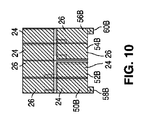
- 各LEDについて、前記nコンタクトは、互いに電気的に接続される複数の第1の領域に分割され、前記pコンタクトは、互いに電気的に接続される複数の第2の領域に分割される、請求項2に記載の発光デバイス。
- 前記マウントは、絶縁体の上部表面に配設される第3の領域を含み、
前記第3の領域は、前記第1の領域及び前記第2の領域に整合し、
前記第1の領域及び前記第2の領域は、前記第1の向き及び前記第2の向きにおいて、異なる第3の領域に整合する、
請求項5に記載の発光デバイス。 - 前記第1の向きにおいて、前記発光構造の前記複数のLEDのうち少なくとも2つが直列に接続され、
前記第2の向きにおいて、前記発光構造の前記複数のLEDのうち少なくとも2つが並列に接続される、
請求項2に記載の発光デバイス。 - 発光構造であって、
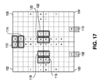
複数の発光ダイオード(LED)であり、各LEDはn型領域とp型領域との間に配設される発光層を含む、複数のLEDと、
前記p型領域上に配設されるpコンタクトと、
前記n型領域上に配設されるnコンタクトと、
を含む、発光構造と、
アノードパッド及びカソードパッドを含むマウントと、
を含み、
前記nコンタクト及び前記pコンタクトは、前記アノードパッドのうち少なくとも1つ及び前記カソードパッドのうち少なくとも1つの上に第1の向きにおいて、又は前記アノードパッドのうち少なくとも1つ及び前記カソードパッドのうち少なくとも1つの上に第2の向きにおいてのいずれかで前記マウントに付けられ、
前記マウント上の少なくとも2つのLEDにおける少なくとも1つの電気的接続であり、前記少なくとも2つのLEDは、前記第1の向きにおいて前記少なくとも1つの電気的接続を介して直列に接続され、前記少なくとも2つのLEDは、前記第2の向きにおいて前記少なくとも1つの電気的接続を介して並列に接続される、少なくとも1つの電気的接続、を含む、
発光デバイス。
Priority Applications (1)
| Application Number | Priority Date | Filing Date | Title |
|---|---|---|---|
| JP2020005552A JP6928128B2 (ja) | 2013-03-15 | 2020-01-17 | 発光構造及びマウント |
Applications Claiming Priority (3)
| Application Number | Priority Date | Filing Date | Title |
|---|---|---|---|
| US201361798858P | 2013-03-15 | 2013-03-15 | |
| US61/798,858 | 2013-03-15 | ||
| PCT/IB2014/059466 WO2014141009A1 (en) | 2013-03-15 | 2014-03-05 | Light emitting structure and mount |
Related Child Applications (1)
| Application Number | Title | Priority Date | Filing Date |
|---|---|---|---|
| JP2020005552A Division JP6928128B2 (ja) | 2013-03-15 | 2020-01-17 | 発光構造及びマウント |
Publications (3)
| Publication Number | Publication Date |
|---|---|
| JP2016510180A JP2016510180A (ja) | 2016-04-04 |
| JP2016510180A5 JP2016510180A5 (ja) | 2017-05-18 |
| JP6649773B2 true JP6649773B2 (ja) | 2020-02-19 |
Family
ID=50390146
Family Applications (2)
| Application Number | Title | Priority Date | Filing Date |
|---|---|---|---|
| JP2015562452A Active JP6649773B2 (ja) | 2013-03-15 | 2014-03-05 | 発光構造及びマウント |
| JP2020005552A Active JP6928128B2 (ja) | 2013-03-15 | 2020-01-17 | 発光構造及びマウント |
Family Applications After (1)
| Application Number | Title | Priority Date | Filing Date |
|---|---|---|---|
| JP2020005552A Active JP6928128B2 (ja) | 2013-03-15 | 2020-01-17 | 発光構造及びマウント |
Country Status (7)
| Country | Link |
|---|---|
| US (2) | US9478712B2 (ja) |
| EP (1) | EP2973714B1 (ja) |
| JP (2) | JP6649773B2 (ja) |
| KR (1) | KR101991960B1 (ja) |
| CN (1) | CN105190893B (ja) |
| TW (1) | TWI627739B (ja) |
| WO (1) | WO2014141009A1 (ja) |
Families Citing this family (5)
| Publication number | Priority date | Publication date | Assignee | Title |
|---|---|---|---|---|
| JP6927970B2 (ja) * | 2015-11-20 | 2021-09-01 | ルミレッズ ホールディング ベーフェー | 異なる電気的構成を可能にするダイボンドパッド設計 |
| CN109314160B (zh) * | 2015-11-20 | 2021-08-24 | 亮锐控股有限公司 | 为实现不同的电配置的管芯接合焊盘设计 |
| JP7114854B2 (ja) * | 2020-04-28 | 2022-08-09 | 日亜化学工業株式会社 | 発光装置 |
| EP4160679B1 (en) | 2020-04-28 | 2024-01-31 | Nichia Corporation | Light-emitting device |
| CN111987200B (zh) * | 2020-08-20 | 2022-07-01 | 厦门三安光电有限公司 | 发光二极管模组、背光模组和显示模组 |
Family Cites Families (18)
| Publication number | Priority date | Publication date | Assignee | Title |
|---|---|---|---|---|
| US6547249B2 (en) | 2001-03-29 | 2003-04-15 | Lumileds Lighting U.S., Llc | Monolithic series/parallel led arrays formed on highly resistive substrates |
| JP4254141B2 (ja) * | 2001-07-30 | 2009-04-15 | 日亜化学工業株式会社 | 発光装置 |
| JP4438492B2 (ja) * | 2003-09-11 | 2010-03-24 | 日亜化学工業株式会社 | 半導体装置およびその製造方法 |
| US8076680B2 (en) * | 2005-03-11 | 2011-12-13 | Seoul Semiconductor Co., Ltd. | LED package having an array of light emitting cells coupled in series |
| EP1905102B1 (en) * | 2005-06-28 | 2018-08-29 | Seoul Viosys Co., Ltd | Light emitting device for ac power operation |
| WO2007018360A1 (en) * | 2005-08-09 | 2007-02-15 | Seoul Opto Device Co., Ltd. | Ac light emitting diode and method for fabricating the same |
| JP4856463B2 (ja) | 2005-10-17 | 2012-01-18 | 株式会社 日立ディスプレイズ | 液晶表示装置 |
| US7910395B2 (en) * | 2006-09-13 | 2011-03-22 | Helio Optoelectronics Corporation | LED structure |
| US10295147B2 (en) * | 2006-11-09 | 2019-05-21 | Cree, Inc. | LED array and method for fabricating same |
| TWI419360B (zh) | 2008-08-11 | 2013-12-11 | Formosa Epitaxy Inc | Solid crystal light-emitting device having an insulating layer and a method for manufacturing the same |
| US8648359B2 (en) * | 2010-06-28 | 2014-02-11 | Cree, Inc. | Light emitting devices and methods |
| JP2012028749A (ja) * | 2010-07-22 | 2012-02-09 | Seoul Opto Devices Co Ltd | 発光ダイオード |
| TWI472058B (zh) * | 2010-10-13 | 2015-02-01 | Interlight Optotech Corp | 發光二極體裝置 |
| US9053958B2 (en) * | 2011-01-31 | 2015-06-09 | Cree, Inc. | Light emitting diode (LED) arrays including direct die attach and related assemblies |
| WO2013035024A1 (en) * | 2011-09-06 | 2013-03-14 | Koninklijke Philips Electronics N.V. | Topology of distributing and connecting leds in a large area matrix |
| US8760068B1 (en) * | 2011-09-07 | 2014-06-24 | Iml International | Driving LEDs in LCD backlight |
| JP2013118292A (ja) * | 2011-12-02 | 2013-06-13 | Citizen Electronics Co Ltd | Led発光装置 |
| US9039746B2 (en) * | 2013-02-08 | 2015-05-26 | Cree, Inc. | Solid state light emitting devices including adjustable melatonin suppression effects |
-
2014
- 2014-03-05 EP EP14713589.1A patent/EP2973714B1/en active Active
- 2014-03-05 CN CN201480016065.3A patent/CN105190893B/zh active Active
- 2014-03-05 WO PCT/IB2014/059466 patent/WO2014141009A1/en active Application Filing
- 2014-03-05 JP JP2015562452A patent/JP6649773B2/ja active Active
- 2014-03-05 KR KR1020157029226A patent/KR101991960B1/ko active IP Right Grant
- 2014-03-05 US US14/764,202 patent/US9478712B2/en active Active
- 2014-03-14 TW TW103109278A patent/TWI627739B/zh active
-
2016
- 2016-10-06 US US15/287,623 patent/US10134805B2/en active Active
-
2020
- 2020-01-17 JP JP2020005552A patent/JP6928128B2/ja active Active
Also Published As
| Publication number | Publication date |
|---|---|
| US20150380610A1 (en) | 2015-12-31 |
| US9478712B2 (en) | 2016-10-25 |
| US10134805B2 (en) | 2018-11-20 |
| CN105190893B (zh) | 2018-11-13 |
| WO2014141009A1 (en) | 2014-09-18 |
| US20170025470A1 (en) | 2017-01-26 |
| EP2973714A1 (en) | 2016-01-20 |
| KR101991960B1 (ko) | 2019-06-25 |
| EP2973714B1 (en) | 2019-05-08 |
| TWI627739B (zh) | 2018-06-21 |
| JP2020057821A (ja) | 2020-04-09 |
| CN105190893A (zh) | 2015-12-23 |
| JP6928128B2 (ja) | 2021-09-01 |
| KR20150132410A (ko) | 2015-11-25 |
| JP2016510180A (ja) | 2016-04-04 |
| TW201503339A (zh) | 2015-01-16 |
Similar Documents
| Publication | Publication Date | Title |
|---|---|---|
| JP6928128B2 (ja) | 発光構造及びマウント | |
| US11038081B2 (en) | Method of separating light emitting devices formed on a substrate wafer | |
| US6547249B2 (en) | Monolithic series/parallel led arrays formed on highly resistive substrates | |
| US20150021626A1 (en) | Light-emitting device | |
| US20090039359A1 (en) | Light emitting diode with improved current spreading performance | |
| JP2006108698A (ja) | フリップチップ発光デバイス用のコンタクト及び全方向反射ミラー | |
| US8405101B2 (en) | Semiconductor light emitting device and method of manufacturing the same | |
| US7902562B2 (en) | Light emitting diode device that includes a three dimensional cloud structure and manufacturing method thereof | |
| WO2012030527A1 (en) | Solid state lighting devices with point contacts and associated methods of manufacturing | |
| US20120241786A1 (en) | Solid state optoelectronic device with plated support substrate | |
| KR100872276B1 (ko) | 수직구조 질화물 반도체 발광 소자 및 제조방법 | |
| US20150372054A1 (en) | Monolithic semiconductor chip array | |
| RU2523777C2 (ru) | Продолжение контактных площадок до края кристалла с электрической изоляцией | |
| KR20090076163A (ko) | 질화물 반도체 발광소자 제조방법 및 이에 의해 제조된질화물 반도체 발광소자 | |
| KR20160023560A (ko) | 반도체 발광 소자 | |
| JP5772213B2 (ja) | 発光素子 | |
| JP5098482B2 (ja) | 発光装置の製造方法及び発光装置 | |
| JP2010177446A (ja) | 発光素子 | |
| KR101154509B1 (ko) | 고효율 발광 다이오드 | |
| KR100856267B1 (ko) | 수직구조 질화물 반도체 발광 소자 및 제조방법 | |
| KR20200062537A (ko) | 반도체 발광소자 및 이의 제조방법 | |
| KR20130070292A (ko) | 반극성 발광 다이오드 |
Legal Events
| Date | Code | Title | Description |
|---|---|---|---|
| A621 | Written request for application examination |
Free format text: JAPANESE INTERMEDIATE CODE: A621 Effective date: 20170303 |
|
| A521 | Request for written amendment filed |
Free format text: JAPANESE INTERMEDIATE CODE: A523 Effective date: 20170328 |
|
| A977 | Report on retrieval |
Free format text: JAPANESE INTERMEDIATE CODE: A971007 Effective date: 20171227 |
|
| A131 | Notification of reasons for refusal |
Free format text: JAPANESE INTERMEDIATE CODE: A131 Effective date: 20180109 |
|
| A521 | Request for written amendment filed |
Free format text: JAPANESE INTERMEDIATE CODE: A523 Effective date: 20180406 |
|
| A131 | Notification of reasons for refusal |
Free format text: JAPANESE INTERMEDIATE CODE: A131 Effective date: 20180904 |
|
| A521 | Request for written amendment filed |
Free format text: JAPANESE INTERMEDIATE CODE: A523 Effective date: 20181129 |
|
| A711 | Notification of change in applicant |
Free format text: JAPANESE INTERMEDIATE CODE: A711 Effective date: 20190307 |
|
| A131 | Notification of reasons for refusal |
Free format text: JAPANESE INTERMEDIATE CODE: A131 Effective date: 20190507 |
|
| A601 | Written request for extension of time |
Free format text: JAPANESE INTERMEDIATE CODE: A601 Effective date: 20190806 |
|
| A521 | Request for written amendment filed |
Free format text: JAPANESE INTERMEDIATE CODE: A523 Effective date: 20191107 |
|
| TRDD | Decision of grant or rejection written | ||
| A01 | Written decision to grant a patent or to grant a registration (utility model) |
Free format text: JAPANESE INTERMEDIATE CODE: A01 Effective date: 20191119 |
|
| A601 | Written request for extension of time |
Free format text: JAPANESE INTERMEDIATE CODE: A601 Effective date: 20191206 |
|
| A61 | First payment of annual fees (during grant procedure) |
Free format text: JAPANESE INTERMEDIATE CODE: A61 Effective date: 20200117 |
|
| R150 | Certificate of patent or registration of utility model |
Ref document number: 6649773 Country of ref document: JP Free format text: JAPANESE INTERMEDIATE CODE: R150 |
|
| R250 | Receipt of annual fees |
Free format text: JAPANESE INTERMEDIATE CODE: R250 |
|
| R250 | Receipt of annual fees |
Free format text: JAPANESE INTERMEDIATE CODE: R250 |