JP6649552B2 - 前面パターニングの調整を決定する基板の背面のテクスチャマップを生成するシステム及び方法 - Google Patents
前面パターニングの調整を決定する基板の背面のテクスチャマップを生成するシステム及び方法 Download PDFInfo
- Publication number
- JP6649552B2 JP6649552B2 JP2016548098A JP2016548098A JP6649552B2 JP 6649552 B2 JP6649552 B2 JP 6649552B2 JP 2016548098 A JP2016548098 A JP 2016548098A JP 2016548098 A JP2016548098 A JP 2016548098A JP 6649552 B2 JP6649552 B2 JP 6649552B2
- Authority
- JP
- Japan
- Prior art keywords
- substrate
- surface roughness
- sensor
- texture map
- profile
- Prior art date
- Legal status (The legal status is an assumption and is not a legal conclusion. Google has not performed a legal analysis and makes no representation as to the accuracy of the status listed.)
- Active
Links
Images


Classifications
-
- H—ELECTRICITY
- H10—SEMICONDUCTOR DEVICES; ELECTRIC SOLID-STATE DEVICES NOT OTHERWISE PROVIDED FOR
- H10P—GENERIC PROCESSES OR APPARATUS FOR THE MANUFACTURE OR TREATMENT OF DEVICES COVERED BY CLASS H10
- H10P74/00—Testing or measuring during manufacture or treatment of wafers, substrates or devices
- H10P74/20—Testing or measuring during manufacture or treatment of wafers, substrates or devices characterised by the properties tested or measured, e.g. structural or electrical properties
- H10P74/203—Structural properties, e.g. testing or measuring thicknesses, line widths, warpage, bond strengths or physical defects
-
- H—ELECTRICITY
- H10—SEMICONDUCTOR DEVICES; ELECTRIC SOLID-STATE DEVICES NOT OTHERWISE PROVIDED FOR
- H10P—GENERIC PROCESSES OR APPARATUS FOR THE MANUFACTURE OR TREATMENT OF DEVICES COVERED BY CLASS H10
- H10P72/00—Handling or holding of wafers, substrates or devices during manufacture or treatment thereof
- H10P72/06—Apparatus for monitoring, sorting, marking, testing or measuring
- H10P72/0616—Monitoring of warpages, curvatures, damages, defects or the like
-
- H—ELECTRICITY
- H10—SEMICONDUCTOR DEVICES; ELECTRIC SOLID-STATE DEVICES NOT OTHERWISE PROVIDED FOR
- H10P—GENERIC PROCESSES OR APPARATUS FOR THE MANUFACTURE OR TREATMENT OF DEVICES COVERED BY CLASS H10
- H10P72/00—Handling or holding of wafers, substrates or devices during manufacture or treatment thereof
- H10P72/50—Handling or holding of wafers, substrates or devices during manufacture or treatment thereof for positioning, orientation or alignment
-
- H—ELECTRICITY
- H10—SEMICONDUCTOR DEVICES; ELECTRIC SOLID-STATE DEVICES NOT OTHERWISE PROVIDED FOR
- H10P—GENERIC PROCESSES OR APPARATUS FOR THE MANUFACTURE OR TREATMENT OF DEVICES COVERED BY CLASS H10
- H10P74/00—Testing or measuring during manufacture or treatment of wafers, substrates or devices
- H10P74/23—Testing or measuring during manufacture or treatment of wafers, substrates or devices characterised by multiple measurements, corrections, marking or sorting processes
Landscapes
- Length Measuring Devices With Unspecified Measuring Means (AREA)
- A Measuring Device Byusing Mechanical Method (AREA)
- Exposure And Positioning Against Photoresist Photosensitive Materials (AREA)
- Physics & Mathematics (AREA)
- General Physics & Mathematics (AREA)
Description

Claims (18)
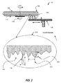
- 軸まわりに基板を回転させることが可能な基板チャックであって、該基板は、背面とは反対にある、パターンが形成される前面を含む、基板チャックと、
前記基板の背面を横切って動き、前記基板の背面の表面粗さに基づいたプロファイル信号を生成することが可能な、前記基板の背面の表面粗さについてのプロファイルセンサと、
前記基板に対する前記プロファイルセンサの位置に基づいた位置信号を生成することが可能な位置コントローラと、
前記プロファイル信号及び前記位置信号に基づいた、前記基板の背面のテクスチャマップであって、該テクスチャマップは、前記基板の背面の位置についての表面粗さの指標を含む、テクスチャマップを生成することが可能なテクスチャマップコンポーネントと、を含み、
前記プロファイルセンサは、
前記基板の背面と接触することが可能な接触エレメントと、
前記接触エレメントに結合した検出コンポーネントであって、該検出コンポーネントは圧力又は力が前記接触エレメントに加えられたときの前記プロファイル信号を生成することが可能な検出コンポーネントと、を含む、テクスチャマッピングシステム。 - 前記表面粗さは、前記基板の背面の複数の振幅に基づいた、請求項1に記載のシステム。
- 前記表面粗さは、前記背面のフィーチャの複数の振幅及び周期に基づいた、請求項1に記載のシステム。
- 前記プロファイルセンサは、前記背面と異なる位置で接触することができる二つ以上の接触エレメントを含み、
前記接触エレメントは、該接触エレメントについての前記プロファイル信号を生成する、対応する検出コンポーネントに結合した、請求項1に記載のシステム。 - 前記テクスチャマップコンポーネントは、前記二つ以上の接触エレメントからの前記プロファイル信号の組み合わせに基づいた前記テクスチャマップを生成する、請求項4に記載のシステム。
- 前記テクスチャマップコンポーネントは、前記二つ以上の接触エレメントからの前記位置信号の組み合わせに基づいた前記テクスチャマップを生成する、請求項5に記載のシステム。
- 前記基板チャックは、毎分60回転以上で回転することが可能である、請求項1に記載のシステム。
- 前記基板の背面を横切って前記プロファイルセンサを移動させることが可能な移動アームをさらに含む、請求項1に記載のシステム。
- 前記プロファイルセンサに結合した移動アームをさらに含み、該移動アームは前記プロファイルセンサが前記基板の背面に接触するように動かすことが可能である、請求項1に記載のシステム。
- 基板の表面粗さをマッピングする方法であって、
基板チャックを使用して、前記基板の中央領域に近接した軸まわりに前記基板を回転させる工程であって、前記基板は、背面とは反対にある、パターンが形成される前面を含む、工程と、
表面粗さセンサを回転している前記基板の背面を横切って動かす工程であって、該表面粗さセンサは前記背面の表面のフィーチャの振幅又は周波数を検出することが可能である、工程と、
前記表面粗さセンサを用いて、前記基板の背面のフィーチャの検出した振幅又は周波数に基づいて、プロファイル信号を生成する工程と、
コンピュータプロセッサを用いて、検出された前記背面のフィーチャの振幅又は周波数に基づいた、前記基板の背面のテクスチャマップを生成する工程と、を含み、
前記表面粗さセンサは、
前記基板の背面と接触することが可能な接触エレメントと、
前記接触エレメントに結合した検出コンポーネントであって、該検出コンポーネントは圧力又は力が前記接触エレメントに加えられたときの前記プロファイル信号を生成することが可能な検出コンポーネントと、を含む、方法。 - 前記テクスチャマップは、前記表面粗さセンサが基板に接触した座標情報及び該座標情報での又はその近傍の前記フィーチャの振幅又は周波数を含む、請求項10に記載の方法。
- 位置センサを用いて、前記表面粗さセンサが、前記基板のフィーチャの検出した振幅又は周波数の位置に基づいて、位置信号を生成する工程と、をさらに含む請求項10に記載の方法。
- 前記テクスチャマップは、前記基板の背面の位置での表面粗さの指標を提供し得る、請求項10に記載の方法。
- 位置信号は、前記基板の回転方向の移動と前記表面粗さセンサの線形移動とに基づいた座標情報を含む、請求項10に記載の方法。
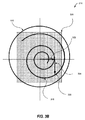
- 前記テクスチャマップは、前記背面の表面の表面粗さの境界プロットを含む、請求項14に記載の方法。
- 前記テクスチャマップでの前記背面の座標位置を前記前面の座標位置に関連づけて、前記前面の座標位置についてのオフセット調整を決定することが可能な調整コンポーネントに前記テクスチャマップを提供する工程を、さらに含む、請求項10に記載の方法。
- 前記オフセット調整は、座標及び表面粗さの値の少なくとも一つに対応する焦点深度の調整値を含む、請求項16に記載の方法。
- 前記回転は、毎分5回転(rpm)と60rpmとの間の回転速度を含む、請求項16に記載の方法。
Applications Claiming Priority (3)
| Application Number | Priority Date | Filing Date | Title |
|---|---|---|---|
| US201461931555P | 2014-01-24 | 2014-01-24 | |
| US61/931,555 | 2014-01-24 | ||
| PCT/US2015/012726 WO2015112884A1 (en) | 2014-01-24 | 2015-01-23 | Systems and methods for generating backside substrate texture maps for determining adjustments for front side patterning |
Publications (2)
| Publication Number | Publication Date |
|---|---|
| JP2017505438A JP2017505438A (ja) | 2017-02-16 |
| JP6649552B2 true JP6649552B2 (ja) | 2020-02-19 |
Family
ID=53678723
Family Applications (1)
| Application Number | Title | Priority Date | Filing Date |
|---|---|---|---|
| JP2016548098A Active JP6649552B2 (ja) | 2014-01-24 | 2015-01-23 | 前面パターニングの調整を決定する基板の背面のテクスチャマップを生成するシステム及び方法 |
Country Status (6)
| Country | Link |
|---|---|
| US (1) | US20150211836A1 (ja) |
| JP (1) | JP6649552B2 (ja) |
| KR (1) | KR20160111512A (ja) |
| CN (1) | CN105934812A (ja) |
| TW (1) | TWI560750B (ja) |
| WO (1) | WO2015112884A1 (ja) |
Families Citing this family (9)
| Publication number | Priority date | Publication date | Assignee | Title |
|---|---|---|---|---|
| JP6267141B2 (ja) * | 2014-06-04 | 2018-01-24 | 東京エレクトロン株式会社 | 液塗布方法、液塗布装置、及びコンピュータ読み取り可能な記録媒体 |
| KR101996492B1 (ko) | 2014-12-01 | 2019-07-04 | 에이에스엠엘 네델란즈 비.브이. | 리소그래피 제조 프로세스에 관련된 진단 정보를 획득하기 위한 방법 및 장치, 진단 장치를 포함하는 리소그래피 처리 시스템 |
| KR20170130674A (ko) * | 2016-05-18 | 2017-11-29 | 삼성전자주식회사 | 공정 평가 방법 및 그를 포함하는 기판 제조 장치의 제어 방법 |
| US10770327B2 (en) * | 2017-07-28 | 2020-09-08 | Taiwan Semiconductor Manufacturing Co., Ltd. | System and method for correcting non-ideal wafer topography |
| JP7012538B2 (ja) * | 2018-01-11 | 2022-01-28 | 株式会社ディスコ | ウエーハの評価方法 |
| FI128841B (en) * | 2018-03-22 | 2021-01-15 | Univ Helsinki | Sensor calibration |
| US11036147B2 (en) * | 2019-03-20 | 2021-06-15 | Kla Corporation | System and method for converting backside surface roughness to frontside overlay |
| US12469725B2 (en) | 2021-06-27 | 2025-11-11 | Delta Design, Inc. | Method for determining corrective film pattern to reduce semiconductor wafer bow |
| US20250164238A1 (en) * | 2023-11-16 | 2025-05-22 | Applied Materials, Inc. | Surface roughness and emissivity determination |
Family Cites Families (21)
| Publication number | Priority date | Publication date | Assignee | Title |
|---|---|---|---|---|
| JP4207976B2 (ja) * | 2006-05-17 | 2009-01-14 | 住友電気工業株式会社 | 化合物半導体基板の表面処理方法、および化合物半導体結晶の製造方法 |
| JPS54153290U (ja) * | 1978-04-14 | 1979-10-24 | ||
| CA1143869A (en) * | 1980-10-01 | 1983-03-29 | Northern Telecom Limited | Surface relief measuring equipment |
| US4504144A (en) * | 1982-07-06 | 1985-03-12 | The Perkin-Elmer Corporation | Simple electromechanical tilt and focus device |
| US4750141A (en) * | 1985-11-26 | 1988-06-07 | Ade Corporation | Method and apparatus for separating fixture-induced error from measured object characteristics and for compensating the measured object characteristic with the error, and a bow/warp station implementing same |
| US4931962A (en) * | 1988-05-13 | 1990-06-05 | Ade Corporation | Fixture and nonrepeatable error compensation system |
| US5446824A (en) * | 1991-10-11 | 1995-08-29 | Texas Instruments | Lamp-heated chuck for uniform wafer processing |
| JP2000180157A (ja) * | 1998-12-16 | 2000-06-30 | Super Silicon Kenkyusho:Kk | 平坦度測定センサ |
| SE514309C2 (sv) * | 1999-05-28 | 2001-02-05 | Ericsson Telefon Ab L M | Förfarande för att bestämma ytstruktur |
| JP2002033268A (ja) * | 2000-07-18 | 2002-01-31 | Nikon Corp | 表面形状測定方法及びこれを用いた露光方法とデバイスの製造方法 |
| JP4380039B2 (ja) * | 2000-08-22 | 2009-12-09 | ソニー株式会社 | 半導体装置の製造方法および半導体製造装置 |
| US6624078B1 (en) * | 2001-07-13 | 2003-09-23 | Lam Research Corporation | Methods for analyzing the effectiveness of wafer backside cleaning |
| SG129992A1 (en) * | 2001-08-13 | 2007-03-20 | Micron Technology Inc | Method and apparatus for detecting topographical features of microelectronic substrates |
| JP2003317285A (ja) * | 2002-04-25 | 2003-11-07 | Ricoh Co Ltd | 光ディスク原盤露光装置および光ディスク原盤露光方法、並びに回転振れ検出方法 |
| US7968354B1 (en) * | 2002-10-04 | 2011-06-28 | Kla-Tencor Technologies Corp. | Methods for correlating backside and frontside defects detected on a specimen and classification of backside defects |
| US7760347B2 (en) * | 2005-05-13 | 2010-07-20 | Applied Materials, Inc. | Design-based method for grouping systematic defects in lithography pattern writing system |
| US7348556B2 (en) * | 2005-07-19 | 2008-03-25 | Fei Company | Method of measuring three-dimensional surface roughness of a structure |
| JP5009564B2 (ja) * | 2006-07-20 | 2012-08-22 | 株式会社ミツトヨ | 表面追従型測定器 |
| JP4788785B2 (ja) * | 2009-02-06 | 2011-10-05 | 東京エレクトロン株式会社 | 現像装置、現像処理方法及び記憶媒体 |
| WO2012008484A1 (ja) * | 2010-07-14 | 2012-01-19 | 国立大学法人静岡大学 | 接触状態検出装置、接触状態検出方法、接触状態検出用コンピュータプログラム、接触状態検出装置を備える電気伝導度測定システムおよび接触状態検出方法を含む電気伝導度測定方法 |
| US9354526B2 (en) * | 2011-10-11 | 2016-05-31 | Kla-Tencor Corporation | Overlay and semiconductor process control using a wafer geometry metric |
-
2015
- 2015-01-23 US US14/604,393 patent/US20150211836A1/en not_active Abandoned
- 2015-01-23 KR KR1020167023126A patent/KR20160111512A/ko not_active Ceased
- 2015-01-23 JP JP2016548098A patent/JP6649552B2/ja active Active
- 2015-01-23 WO PCT/US2015/012726 patent/WO2015112884A1/en not_active Ceased
- 2015-01-23 CN CN201580005769.5A patent/CN105934812A/zh active Pending
- 2015-01-26 TW TW104102481A patent/TWI560750B/zh not_active IP Right Cessation
Also Published As
| Publication number | Publication date |
|---|---|
| US20150211836A1 (en) | 2015-07-30 |
| JP2017505438A (ja) | 2017-02-16 |
| TW201545203A (zh) | 2015-12-01 |
| CN105934812A (zh) | 2016-09-07 |
| KR20160111512A (ko) | 2016-09-26 |
| TWI560750B (en) | 2016-12-01 |
| WO2015112884A1 (en) | 2015-07-30 |
Similar Documents
| Publication | Publication Date | Title |
|---|---|---|
| JP6649552B2 (ja) | 前面パターニングの調整を決定する基板の背面のテクスチャマップを生成するシステム及び方法 | |
| CN110672040B (zh) | 一种基于视觉的高精度旋转角度测量方法 | |
| JP5760129B2 (ja) | 基板表面の欠陥検査方法及び装置 | |
| JP4896373B2 (ja) | 立体3次元計測システムおよび方法 | |
| JP4486991B2 (ja) | 新校正方法を使った形状精度の改良 | |
| JP6815336B2 (ja) | 静的縞パターンを使用した干渉ロールオフ測定 | |
| US10102631B2 (en) | Edge detection bias correction value calculation method, edge detection bias correction method, and edge detection bias correcting program | |
| JP2005514606A5 (ja) | ||
| JP2009092488A (ja) | 三次元形状測定方法 | |
| CN109870129A (zh) | 一种基于相位偏折原理的晶圆表面粗糙度检测装置 | |
| CN110207584B (zh) | 一种膜厚测量方法、系统及化学机械抛光装置 | |
| CN106168464A (zh) | 一种基于机器视觉的主轴动态回转精度测试方法 | |
| CN105444673A (zh) | 旋转平移绝对检测法中确定光学元件中心的装置及方法 | |
| CN112697063B (zh) | 一种基于显微视觉的芯片应变测量方法 | |
| CN107883964B (zh) | 环抛加工中工件环上单点运动轨迹检测装置及利用该装置进行检测的方法 | |
| CN102642155B (zh) | 一种基于图像辅助的微小零件回转调心方法 | |
| JP2017116401A (ja) | 基板位置調整装置および基板位置調整方法 | |
| US20090024351A1 (en) | Method for Determining Correction Values for the Measured Values of Positions of Structures on a Substrate | |
| CN112556614B (zh) | 转换关系的获取方法、测量方法及测量系统 | |
| CN108761137B (zh) | Afm针尖磨损测量方法 | |
| JP5030917B2 (ja) | 姿勢測定方法及び研削装置 | |
| JP2016095243A (ja) | 計測装置、計測方法、および物品の製造方法 | |
| JP5087165B1 (ja) | 表面検査装置を調整するためのデータを出力する調整装置、調整データ出力方法及びプログラム | |
| CN118500264B (zh) | 基于激光三角法的速度和距离同步测量系统及方法 | |
| CN119374870B (zh) | 一种视向角检测方法及系统 |
Legal Events
| Date | Code | Title | Description |
|---|---|---|---|
| A621 | Written request for application examination |
Free format text: JAPANESE INTERMEDIATE CODE: A621 Effective date: 20180109 |
|
| A131 | Notification of reasons for refusal |
Free format text: JAPANESE INTERMEDIATE CODE: A131 Effective date: 20181218 |
|
| A601 | Written request for extension of time |
Free format text: JAPANESE INTERMEDIATE CODE: A601 Effective date: 20190313 |
|
| A521 | Request for written amendment filed |
Free format text: JAPANESE INTERMEDIATE CODE: A523 Effective date: 20190517 |
|
| A02 | Decision of refusal |
Free format text: JAPANESE INTERMEDIATE CODE: A02 Effective date: 20190611 |
|
| A521 | Request for written amendment filed |
Free format text: JAPANESE INTERMEDIATE CODE: A523 Effective date: 20191011 |
|
| A911 | Transfer to examiner for re-examination before appeal (zenchi) |
Free format text: JAPANESE INTERMEDIATE CODE: A911 Effective date: 20191021 |
|
| TRDD | Decision of grant or rejection written | ||
| A01 | Written decision to grant a patent or to grant a registration (utility model) |
Free format text: JAPANESE INTERMEDIATE CODE: A01 Effective date: 20191112 |
|
| A711 | Notification of change in applicant |
Free format text: JAPANESE INTERMEDIATE CODE: A711 Effective date: 20191210 |
|
| A61 | First payment of annual fees (during grant procedure) |
Free format text: JAPANESE INTERMEDIATE CODE: A61 Effective date: 20191210 |
|
| R150 | Certificate of patent or registration of utility model |
Ref document number: 6649552 Country of ref document: JP Free format text: JAPANESE INTERMEDIATE CODE: R150 |
|
| R250 | Receipt of annual fees |
Free format text: JAPANESE INTERMEDIATE CODE: R250 |
|
| R250 | Receipt of annual fees |
Free format text: JAPANESE INTERMEDIATE CODE: R250 |
|
| R250 | Receipt of annual fees |
Free format text: JAPANESE INTERMEDIATE CODE: R250 |