JP6643255B2 - Rcネットワークをもつ多段増幅器 - Google Patents
Rcネットワークをもつ多段増幅器 Download PDFInfo
- Publication number
- JP6643255B2 JP6643255B2 JP2016568627A JP2016568627A JP6643255B2 JP 6643255 B2 JP6643255 B2 JP 6643255B2 JP 2016568627 A JP2016568627 A JP 2016568627A JP 2016568627 A JP2016568627 A JP 2016568627A JP 6643255 B2 JP6643255 B2 JP 6643255B2
- Authority
- JP
- Japan
- Prior art keywords
- amplifier stage
- coupled
- signal
- amplifier
- input
- Prior art date
- Legal status (The legal status is an assumption and is not a legal conclusion. Google has not performed a legal analysis and makes no representation as to the accuracy of the status listed.)
- Active
Links
- 238000004220 aggregation Methods 0.000 claims description 29
- 230000002776 aggregation Effects 0.000 claims description 28
- 230000009977 dual effect Effects 0.000 claims description 20
- 230000008878 coupling Effects 0.000 claims description 18
- 238000010168 coupling process Methods 0.000 claims description 18
- 238000005859 coupling reaction Methods 0.000 claims description 18
- 239000003990 capacitor Substances 0.000 claims description 17
- 238000000034 method Methods 0.000 claims description 17
- 230000007850 degeneration Effects 0.000 claims description 9
- 230000008859 change Effects 0.000 claims description 4
- 230000003213 activating effect Effects 0.000 claims description 3
- 239000000969 carrier Substances 0.000 description 22
- 238000004891 communication Methods 0.000 description 20
- 230000005540 biological transmission Effects 0.000 description 6
- 238000006243 chemical reaction Methods 0.000 description 6
- 230000008569 process Effects 0.000 description 4
- 238000012545 processing Methods 0.000 description 4
- 230000003321 amplification Effects 0.000 description 3
- 238000010586 diagram Methods 0.000 description 3
- 238000005516 engineering process Methods 0.000 description 3
- 230000006870 function Effects 0.000 description 3
- 238000003199 nucleic acid amplification method Methods 0.000 description 3
- 229910000577 Silicon-germanium Inorganic materials 0.000 description 2
- 230000001413 cellular effect Effects 0.000 description 2
- 239000000835 fiber Substances 0.000 description 2
- 230000003287 optical effect Effects 0.000 description 2
- 238000013515 script Methods 0.000 description 2
- JBRZTFJDHDCESZ-UHFFFAOYSA-N AsGa Chemical compound [As]#[Ga] JBRZTFJDHDCESZ-UHFFFAOYSA-N 0.000 description 1
- LEVVHYCKPQWKOP-UHFFFAOYSA-N [Si].[Ge] Chemical compound [Si].[Ge] LEVVHYCKPQWKOP-UHFFFAOYSA-N 0.000 description 1
- 238000013459 approach Methods 0.000 description 1
- 230000000903 blocking effect Effects 0.000 description 1
- 230000000295 complement effect Effects 0.000 description 1
- 238000004590 computer program Methods 0.000 description 1
- 230000003750 conditioning effect Effects 0.000 description 1
- 230000000694 effects Effects 0.000 description 1
- 238000007667 floating Methods 0.000 description 1
- 239000012212 insulator Substances 0.000 description 1
- 230000007774 longterm Effects 0.000 description 1
- 229910044991 metal oxide Inorganic materials 0.000 description 1
- 150000004706 metal oxides Chemical class 0.000 description 1
- 238000010295 mobile communication Methods 0.000 description 1
- 238000012986 modification Methods 0.000 description 1
- 230000004048 modification Effects 0.000 description 1
- 238000001579 optical reflectometry Methods 0.000 description 1
- 230000000737 periodic effect Effects 0.000 description 1
- 230000000644 propagated effect Effects 0.000 description 1
- 239000004065 semiconductor Substances 0.000 description 1
- 238000000926 separation method Methods 0.000 description 1
- 239000011232 storage material Substances 0.000 description 1
- 238000006467 substitution reaction Methods 0.000 description 1
- 230000001360 synchronised effect Effects 0.000 description 1
- 238000012546 transfer Methods 0.000 description 1
- 230000001052 transient effect Effects 0.000 description 1
Images


Classifications
-
- H—ELECTRICITY
- H04—ELECTRIC COMMUNICATION TECHNIQUE
- H04W—WIRELESS COMMUNICATION NETWORKS
- H04W52/00—Power management, e.g. TPC [Transmission Power Control], power saving or power classes
- H04W52/02—Power saving arrangements
- H04W52/0209—Power saving arrangements in terminal devices
- H04W52/0225—Power saving arrangements in terminal devices using monitoring of external events, e.g. the presence of a signal
- H04W52/0229—Power saving arrangements in terminal devices using monitoring of external events, e.g. the presence of a signal where the received signal is a wanted signal
-
- H—ELECTRICITY
- H04—ELECTRIC COMMUNICATION TECHNIQUE
- H04B—TRANSMISSION
- H04B1/00—Details of transmission systems, not covered by a single one of groups H04B3/00 - H04B13/00; Details of transmission systems not characterised by the medium used for transmission
- H04B1/005—Details of transmission systems, not covered by a single one of groups H04B3/00 - H04B13/00; Details of transmission systems not characterised by the medium used for transmission adapting radio receivers, transmitters andtransceivers for operation on two or more bands, i.e. frequency ranges
-
- H—ELECTRICITY
- H03—ELECTRONIC CIRCUITRY
- H03F—AMPLIFIERS
- H03F1/00—Details of amplifiers with only discharge tubes, only semiconductor devices or only unspecified devices as amplifying elements
- H03F1/56—Modifications of input or output impedances, not otherwise provided for
-
- H—ELECTRICITY
- H03—ELECTRONIC CIRCUITRY
- H03F—AMPLIFIERS
- H03F3/00—Amplifiers with only discharge tubes or only semiconductor devices as amplifying elements
- H03F3/189—High-frequency amplifiers, e.g. radio frequency amplifiers
- H03F3/19—High-frequency amplifiers, e.g. radio frequency amplifiers with semiconductor devices only
-
- H—ELECTRICITY
- H04—ELECTRIC COMMUNICATION TECHNIQUE
- H04B—TRANSMISSION
- H04B1/00—Details of transmission systems, not covered by a single one of groups H04B3/00 - H04B13/00; Details of transmission systems not characterised by the medium used for transmission
- H04B1/38—Transceivers, i.e. devices in which transmitter and receiver form a structural unit and in which at least one part is used for functions of transmitting and receiving
- H04B1/40—Circuits
- H04B1/44—Transmit/receive switching
- H04B1/48—Transmit/receive switching in circuits for connecting transmitter and receiver to a common transmission path, e.g. by energy of transmitter
-
- H—ELECTRICITY
- H03—ELECTRONIC CIRCUITRY
- H03F—AMPLIFIERS
- H03F2200/00—Indexing scheme relating to amplifiers
- H03F2200/294—Indexing scheme relating to amplifiers the amplifier being a low noise amplifier [LNA]
-
- H—ELECTRICITY
- H03—ELECTRONIC CIRCUITRY
- H03F—AMPLIFIERS
- H03F2200/00—Indexing scheme relating to amplifiers
- H03F2200/451—Indexing scheme relating to amplifiers the amplifier being a radio frequency amplifier
-
- H—ELECTRICITY
- H04—ELECTRIC COMMUNICATION TECHNIQUE
- H04W—WIRELESS COMMUNICATION NETWORKS
- H04W88/00—Devices specially adapted for wireless communication networks, e.g. terminals, base stations or access point devices
- H04W88/02—Terminal devices
- H04W88/06—Terminal devices adapted for operation in multiple networks or having at least two operational modes, e.g. multi-mode terminals
-
- Y—GENERAL TAGGING OF NEW TECHNOLOGICAL DEVELOPMENTS; GENERAL TAGGING OF CROSS-SECTIONAL TECHNOLOGIES SPANNING OVER SEVERAL SECTIONS OF THE IPC; TECHNICAL SUBJECTS COVERED BY FORMER USPC CROSS-REFERENCE ART COLLECTIONS [XRACs] AND DIGESTS
- Y02—TECHNOLOGIES OR APPLICATIONS FOR MITIGATION OR ADAPTATION AGAINST CLIMATE CHANGE
- Y02D—CLIMATE CHANGE MITIGATION TECHNOLOGIES IN INFORMATION AND COMMUNICATION TECHNOLOGIES [ICT], I.E. INFORMATION AND COMMUNICATION TECHNOLOGIES AIMING AT THE REDUCTION OF THEIR OWN ENERGY USE
- Y02D30/00—Reducing energy consumption in communication networks
- Y02D30/70—Reducing energy consumption in communication networks in wireless communication networks
Landscapes
- Engineering & Computer Science (AREA)
- Computer Networks & Wireless Communication (AREA)
- Signal Processing (AREA)
- Power Engineering (AREA)
- Amplifiers (AREA)
- Input Circuits Of Receivers And Coupling Of Receivers And Audio Equipment (AREA)
Description
[0001]本出願は、その内容全体が参照により本明細書に明確に組み込まれる、同一出願人が所有する、2014年5月22日に出願された米国仮特許出願第62/001,657号、および2015年3月4日に出願された米国非仮特許出願第14/638,963号の優先権を主張する。
以下に、本願出願の当初の特許請求の範囲に記載された発明を付記する。
[C1]
装置であって、前記装置は下記を備える、
第1のキャリア信号を増幅するように構成された第1の増幅器段と、
第2のキャリア信号を増幅するように構成された第2の増幅器段と、
前記第1の増幅器段に結合され、前記第2の増幅器段に結合された抵抗容量性(RC)ネットワーク、ここで、前記RCネットワークが、容量要素に結合された抵抗要素を含む。
[C2]
第1の負荷回路と第2の負荷回路とをさらに備え、ここにおいて、前記第1の増幅器段が、前記第1の負荷回路に結合された第1のスイッチと、前記第2の負荷回路に結合された第2のスイッチとを含む、C1に記載の装置。
[C3]
前記第2の増幅器段が、前記第1の負荷回路に結合された第3のスイッチと、前記第2の負荷回路に結合された第4のスイッチとを含む、C2に記載の装置。
[C4]
前記第1の増幅器段が、キャリアアグリゲーション動作モードをサポートするように構成され、前記第2の増幅器段が、デュアル加入者識別モジュール(SIM)デュアルスタンバイ(DSDS)動作モードで、ページング信号を検出するために前記第2のキャリア信号を増幅するように構成された、C1に記載の装置。
[C5]
前記RCネットワークが、スイッチングデバイスをさらに含み、前記容量要素が、前記スイッチングデバイスと接地とに結合された、C1に記載の装置。
[C6]
前記スイッチングデバイスは、制御入力に応答し、前記第1の増幅器段が有効にされるかどうかに基づいて前記第2の増幅器段のインピーダンスを変更するように構成される、C5に記載の装置。
[C7]
前記第1の増幅器段および前記第2の増幅器段が、低雑音増幅器(LNA)中に含まれ、ここにおいて、前記LNAは、前記第1の増幅器段が有効にされるかどうかから独立して前記第2の増幅器段を有効にするように構成可能である、C1に記載の装置。
[C8]
前記第1の増幅器段および前記第2の増幅器段は、前記第1の増幅器段および前記第2の増幅器段が有効にされる第1のモードで動作し、および第2のモードで動作するように構成された低雑音増幅器(LNA)中に含まれる、C1に記載の装置。
[C9]
前記第2のモードで、前記第1の増幅器段が無効にされている間に、前記第2の増幅器段が有効にされる、C8に記載の装置。
[C10]
前記第1の増幅器段の入力と前記第2の増幅器段の入力との間の交流(AC)結合を与えるキャパシタをさらに備える、C1に記載の装置。
[C11]
前記第1の増幅器段に結合された第1のバイアス回路と、前記第2の増幅器段に結合された第2のバイアス回路とをさらに備える、C1に記載の装置。
[C12]
前記第1の増幅器段が、第1の利得を与えるように構成され、前記第2の増幅器段が、前記第1の利得とは異なる第2の利得を与えるように構成された、C1に記載の装置。
[C13]
前記第1の増幅器段がディジェネレーション回路を介して接地に結合され、前記第2の増幅器段が接地に直接結合された、C1に記載の装置。
[C14]
装置であって、前記装置は下記を備える、
第1のキャリア信号を増幅するための第1の手段と、
第2のキャリア信号を増幅するための第2の手段と、
抵抗容量性(RC)インピーダンスを与えるための手段、ここで、前記RCインピーダンスを与えるための前記手段が、増幅するための前記第1の手段に結合され、および増幅するための前記第2の手段に結合される。
[C15]
前記RCインピーダンスを与えるための前記手段が、スイッチングのための手段と接地とに結合された容量要素を含む、C14に記載の装置。
[C16]
増幅するための前記第1の手段が、キャリアアグリゲーション動作モードをサポートするように構成され、増幅するための前記第2の手段が、デュアル加入者識別モジュール(SIM)デュアルスタンバイ(DSDS)動作モードで、ページング信号を検出するために前記第2のキャリア信号を増幅するように構成される、C14に記載の装置。
[C17]
増幅するための前記第1の手段の入力と増幅するための前記第2の手段の入力との間の交流(AC)結合を与えるための手段をさらに備える、C14に記載の装置。
[C18]
増幅するための前記第1の手段に結合されたバイアスするための第1の手段と、
増幅するための前記第2の手段に結合されたバイアスするための第2の手段と
をさらに備える、C14に記載の装置。
[C19]
方法であって、前記方法は下記を備える、
第1の増幅器段の入力と第2の増幅器段の入力とにおいて入力信号を受信すること、ここで、前記第1の増幅器段が、第1のキャリア信号を増幅するように構成され、前記第2の増幅器段が、第2のキャリア信号を増幅するように構成される、と、
前記第1の増幅器段に結合され、前記第2の増幅器段に結合された抵抗容量性(RC)ネットワークにおいて、制御入力を受信すること。
[C20]
デュアル加入者識別モジュール(SIM)デュアルスタンバイ(DSDS)動作モードで、前記第1の増幅器段は、前記第1の増幅器段が有効にされたときに、第1のキャリア信号を増幅するように構成され、前記第2の増幅器段は、ページング信号を検出するために第2のキャリア信号を増幅するように構成される、C19に記載の方法。
Claims (13)
- 装置であって、
無線周波数(RF)入力信号の第1のキャリア信号を増幅するように構成された第1の増幅器段と、ここにおいて、前記第1の増幅器段が、キャリアアグリゲーション動作モードをサポートするように構成される、
前記RF入力信号の第2のキャリア信号を増幅するように構成された第2の増幅器段と、ここにおいて、前記第2の増幅器段が、デュアル加入者識別モジュール(SIM)デュアルスタンバイ(DSDS)動作モードで、ページング信号を検出するために前記第2のキャリア信号を増幅するように構成される、
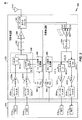
抵抗容量性(RC)ネットワーク、ここで、前記RCネットワークが、前記第1の増幅器段に結合された、及び前記第2の増幅器段に結合された第1の端子を含み、前記RCネットワークが、容量要素に結合された抵抗要素を含み、前記RCネットワークが、前記RF入力信号を受信し、制御入力に応答して前記RF入力信号に接地への経路を与えるように構成され、ここにおいて、前記接地への経路を与えることは、前記第1の増幅器段が有効にされるかどうかに基づいて、前記第2の増幅器段のインピーダンスを変更することを備える、と、
を備え、前記装置は、第1の負荷回路と第2の負荷回路とをさらに備え、ここにおいて、前記第1の増幅器段が、前記第1の増幅器段の出力を前記第1の負荷回路に結合する第1のスイッチと、前記第1の増幅器段の前記出力を前記第2の負荷回路に結合する第2のスイッチとを含む、装置。 - 前記第2の増幅器段が、前記第2の増幅器段の出力を前記第1の負荷回路に結合する第3のスイッチと、前記第2の増幅器段の前記出力を前記第2の負荷回路に結合する第4のスイッチとを含む、請求項1に記載の装置。
- 前記RCネットワークが、
接地に結合された第2の端子と、
制御入力を受信するように構成された第3の端子と
をさらに含み、前記第1の端子が、RF入力ノードにさらに結合される、請求項1に記載の装置。 - 前記RCネットワークが、スイッチングデバイスをさらに含み、前記容量要素が、前記スイッチングデバイスと接地とに結合され、前記スイッチングデバイスが、制御入力に応答し、および前記第1の増幅器段が有効にされるかどうかに基づいて前記第2の増幅器段のインピーダンスを変更するように構成される、請求項1に記載の装置。
- 前記第1の増幅器段および前記第2の増幅器段が、低雑音増幅器(LNA)中に含まれ、ここにおいて、前記LNAが、前記第1の増幅器段が有効にされるかどうかから独立して前記第2の増幅器段を有効にするように構成可能である、請求項1に記載の装置。
- 前記第1の増幅器段および前記第2の増幅器段が、前記第1の増幅器段および前記第2の増幅器段が有効にされる第1のモードで動作し、および第2のモードで動作するように構成された低雑音増幅器(LNA)中に含まれる、請求項1に記載の装置。
- 前記第2のモードで、前記第1の増幅器段が無効にされている間に、前記第2の増幅器段が有効にされる、請求項6に記載の装置。
- 前記第1の増幅器段の入力と前記第2の増幅器段の入力との間の交流(AC)結合を与えるように構成されたキャパシタをさらに備える、請求項1に記載の装置。
- 前記第1の増幅器段に結合された第1のバイアス回路と、前記第2の増幅器段に結合された第2のバイアス回路とをさらに備え、前記第1の増幅器段が、第1の利得を与えるように構成され、前記第2の増幅器段が、前記第1の利得とは異なる第2の利得を与えるように構成される、請求項1に記載の装置。
- 前記RCネットワークが、制御入力を受信するように構成されたトランジスタをさらに含み、前記トランジスタが、前記制御入力を受信するように結合されたゲートと、前記容量要素に結合されたソースと、前記抵抗要素に結合されたドレインとを含む、請求項1に記載の装置。
- 前記第1の増幅器段がディジェネレーション回路を介して接地に結合され、前記第2の増幅器段が接地に直接結合された、請求項1に記載の装置。
- 方法であって、
第1の増幅器段の入力と第2の増幅器段の入力とにおいて入力信号を受信すること、ここで、前記第1の増幅器段が、無線周波数(RF)入力信号の第1のキャリア信号を増幅するように構成され、ここにおいて、前記第1の増幅器段が、キャリアアグリゲーション動作モードをサポートするように構成され、前記第2の増幅器段が、前記RF入力信号の第2のキャリア信号を増幅するように構成される、と、
前記第1の増幅器段の出力を第1の負荷回路に結合するための第1のスイッチを有効にすることと、
前記第1の増幅器段の前記出力を第2の負荷回路に結合するための第2のスイッチを有効にすることと、
前記第1の増幅器段に結合された、及び前記第2の増幅器段に結合された第1の端子を含む抵抗容量性(RC)ネットワークにおいて、制御入力を受信すること、ここで、前記RCネットワークが、前記RF入力信号を受信し、前記制御入力に応答して前記RF入力信号に接地への経路を与え、ここにおいて、デュアル加入者識別モジュール(SIM)デュアルスタンバイ(DSDS)動作モードで、前記第1の増幅器段は、前記第1の増幅器段が有効にされたときに、第1のキャリア信号を増幅するように構成され、前記第2の増幅器段は、ページング信号を検出するために第2のキャリア信号を増幅するように構成され、ここにおいて、前記接地への経路を与えることは、前記第1の増幅器段が有効にされるかどうかに基づいて、前記第2の増幅器段のインピーダンスを変更することを備える、と
を備える、方法。 - 前記第2の増幅器段の出力を第1の負荷回路に結合するための第3のスイッチを有効にすることと、
前記第2の増幅器段の前記出力を第2の負荷回路に結合するための第4のスイッチを有効にすることと
をさらに備える、請求項12に記載の方法。
Applications Claiming Priority (5)
| Application Number | Priority Date | Filing Date | Title |
|---|---|---|---|
| US201462001657P | 2014-05-22 | 2014-05-22 | |
| US62/001,657 | 2014-05-22 | ||
| US14/638,963 | 2015-03-04 | ||
| US14/638,963 US9723560B2 (en) | 2014-05-22 | 2015-03-04 | Multi-stage amplifier with RC network |
| PCT/US2015/029984 WO2015179148A1 (en) | 2014-05-22 | 2015-05-08 | Multi-stage amplifier with rc network |
Publications (3)
| Publication Number | Publication Date |
|---|---|
| JP2017517201A JP2017517201A (ja) | 2017-06-22 |
| JP2017517201A5 JP2017517201A5 (ja) | 2018-05-31 |
| JP6643255B2 true JP6643255B2 (ja) | 2020-02-12 |
Family
ID=53189233
Family Applications (1)
| Application Number | Title | Priority Date | Filing Date |
|---|---|---|---|
| JP2016568627A Active JP6643255B2 (ja) | 2014-05-22 | 2015-05-08 | Rcネットワークをもつ多段増幅器 |
Country Status (6)
| Country | Link |
|---|---|
| US (1) | US9723560B2 (ja) |
| EP (1) | EP3146640B1 (ja) |
| JP (1) | JP6643255B2 (ja) |
| KR (1) | KR102325948B1 (ja) |
| CN (1) | CN106464278B (ja) |
| WO (1) | WO2015179148A1 (ja) |
Families Citing this family (6)
| Publication number | Priority date | Publication date | Assignee | Title |
|---|---|---|---|---|
| TWI619354B (zh) * | 2017-01-26 | 2018-03-21 | 瑞昱半導體股份有限公司 | 射頻收發裝置及其射頻發射機 |
| US11881828B2 (en) | 2017-04-04 | 2024-01-23 | Psemi Corporation | Tunable effective inductance for multi-gain LNA with inductive source degeneration |
| US10038418B1 (en) | 2017-04-04 | 2018-07-31 | Psemi Corporation | Optimized multi gain LNA enabling low current and high linearity including highly linear active bypass |
| WO2020236209A1 (en) * | 2019-05-22 | 2020-11-26 | Adesto Technologies Corporation | Pulse width signal overlap compensation techniques |
| US11159191B1 (en) * | 2020-09-11 | 2021-10-26 | Apple Inc. | Wireless amplifier circuitry for carrier aggregation |
| JP7358316B2 (ja) * | 2020-09-17 | 2023-10-10 | 株式会社東芝 | 半導体回路 |
Family Cites Families (29)
| Publication number | Priority date | Publication date | Assignee | Title |
|---|---|---|---|---|
| WO2002015397A2 (en) | 2000-08-16 | 2002-02-21 | Maxim Integrated Products, Inc. | Low-loss bypass mode of an amplifier with high linearity and matched impedance |
| JP3979485B2 (ja) * | 2001-01-12 | 2007-09-19 | 株式会社ルネサステクノロジ | 信号処理用半導体集積回路および無線通信システム |
| US6914479B1 (en) * | 2002-07-26 | 2005-07-05 | International Business Machines Corporation | Differential amplifier with DC offset cancellation |
| JP4724498B2 (ja) * | 2005-08-30 | 2011-07-13 | ルネサスエレクトロニクス株式会社 | 半導体集積回路装置および高周波電力増幅モジュール |
| JP4712492B2 (ja) * | 2005-08-31 | 2011-06-29 | ルネサスエレクトロニクス株式会社 | 半導体集積回路装置および高周波電力増幅モジュール |
| JP4354465B2 (ja) * | 2006-03-24 | 2009-10-28 | シャープ株式会社 | 可変利得増幅器及びこの可変利得増幅器を備えた通信装置 |
| EP2102992B1 (en) * | 2006-12-21 | 2012-07-04 | Icera Canada ULC | Closed-loop digital power control for a wireless transmitter |
| JP4821618B2 (ja) | 2007-01-15 | 2011-11-24 | パナソニック株式会社 | 高周波電力増幅器のための出力電力検波器 |
| US8086207B2 (en) | 2007-03-19 | 2011-12-27 | Qualcomm Incorporated | Linear transconductor for RF communications |
| US7696828B2 (en) | 2008-01-04 | 2010-04-13 | Qualcomm, Incorporated | Multi-linearity mode LNA having a deboost current path |
| US8433272B2 (en) | 2008-04-15 | 2013-04-30 | Qualcomm Incorporated | Reconfigurable high linearity low noise figure receiver requiring no interstage saw filter |
| US7893855B2 (en) * | 2008-09-16 | 2011-02-22 | Mediatek Inc. | Delta-sigma analog-to-digital converter |
| JP2010109710A (ja) * | 2008-10-30 | 2010-05-13 | New Japan Radio Co Ltd | 利得可変型増幅器 |
| US8754610B2 (en) * | 2009-05-22 | 2014-06-17 | Qualcomm Incorporated | System and method for supplying power to a load |
| US8577325B2 (en) | 2010-08-31 | 2013-11-05 | Korea Advanced Institute Of Science And Technology | Low noise amplifier having both ultra-high linearity and low noise characteristic and radio receiver including the same |
| JP5092046B1 (ja) | 2011-07-29 | 2012-12-05 | 株式会社東芝 | 情報処理装置およびプログラム |
| US8975981B2 (en) | 2011-09-13 | 2015-03-10 | Qualcomm Incorporated | Impedance matching circuits with multiple configurations |
| US9131444B2 (en) | 2011-10-31 | 2015-09-08 | Qualcomm Incorporated | Optimized page matching |
| US8548410B2 (en) * | 2011-11-30 | 2013-10-01 | St-Ericsson Sa | RF front-end for intra-band carrier aggregation |
| US9287906B2 (en) * | 2011-12-19 | 2016-03-15 | Nec Corporation | Transmission apparatus and wireless signal transmission method |
| US9154356B2 (en) * | 2012-05-25 | 2015-10-06 | Qualcomm Incorporated | Low noise amplifiers for carrier aggregation |
| US8909186B2 (en) * | 2012-07-16 | 2014-12-09 | Intel Mobile Communications GmbH | Receiver, method and mobile communication device |
| US8954019B2 (en) * | 2012-08-03 | 2015-02-10 | Blackberry Limited | Mobile wireless communications device with LNA front end circuit and related methods |
| US9543903B2 (en) * | 2012-10-22 | 2017-01-10 | Qualcomm Incorporated | Amplifiers with noise splitting |
| US20140120925A1 (en) * | 2012-11-01 | 2014-05-01 | Qualcomm Incorporated | Mobile station with multi-sim and tune away methods |
| US9603187B2 (en) | 2012-11-14 | 2017-03-21 | Qualcomm Incorporated | Omni-band amplifiers |
| US8903343B2 (en) * | 2013-01-25 | 2014-12-02 | Qualcomm Incorporated | Single-input multiple-output amplifiers with independent gain control per output |
| US9106185B2 (en) | 2013-03-11 | 2015-08-11 | Qualcomm Incorporated | Amplifiers with inductive degeneration and configurable gain and input matching |
| US9124246B2 (en) * | 2013-09-25 | 2015-09-01 | Qualcomm Incorporated | Baseband processing circuitry |
-
2015
- 2015-03-04 US US14/638,963 patent/US9723560B2/en active Active
- 2015-05-08 JP JP2016568627A patent/JP6643255B2/ja active Active
- 2015-05-08 EP EP15723418.8A patent/EP3146640B1/en active Active
- 2015-05-08 CN CN201580026119.9A patent/CN106464278B/zh active Active
- 2015-05-08 KR KR1020167032321A patent/KR102325948B1/ko active IP Right Grant
- 2015-05-08 WO PCT/US2015/029984 patent/WO2015179148A1/en active Application Filing
Also Published As
| Publication number | Publication date |
|---|---|
| CN106464278A (zh) | 2017-02-22 |
| EP3146640A1 (en) | 2017-03-29 |
| KR20170012240A (ko) | 2017-02-02 |
| EP3146640B1 (en) | 2019-06-26 |
| CN106464278B (zh) | 2020-01-03 |
| US9723560B2 (en) | 2017-08-01 |
| WO2015179148A1 (en) | 2015-11-26 |
| JP2017517201A (ja) | 2017-06-22 |
| US20150341859A1 (en) | 2015-11-26 |
| KR102325948B1 (ko) | 2021-11-11 |
Similar Documents
| Publication | Publication Date | Title |
|---|---|---|
| JP6181328B2 (ja) | デュアル利得制御を用いたキャリアアグリゲーション増幅器 | |
| JP6509888B2 (ja) | 電流効率が高い低雑音増幅器(lna) | |
| JP6643255B2 (ja) | Rcネットワークをもつ多段増幅器 | |
| JP6266806B2 (ja) | キャリアアグリゲーション増幅器のためのスプリアス信号低減 | |
| EP3095189B1 (en) | Inter carrier-aggregation isolation in a receiver | |
| JP6208366B2 (ja) | 低雑音増幅器(lna)の非線形2次生成物に関するひずみ消去 | |
| US20200099342A1 (en) | Multi-mode hybrid radio frequency (rf) power amplifier with driver amplifier bypass | |
| US9642166B2 (en) | Cross-connected cascode low noise amplifier for carrier aggregation | |
| US20150163747A1 (en) | Common gate buffer having adjustable current consumption in a receiver | |
| US9130529B2 (en) | Area-efficient degenerative inductance for a low noise amplifier (LNA) |
Legal Events
| Date | Code | Title | Description |
|---|---|---|---|
| A521 | Request for written amendment filed |
Free format text: JAPANESE INTERMEDIATE CODE: A523 Effective date: 20170119 Free format text: JAPANESE INTERMEDIATE CODE: A523 Effective date: 20170120 |
|
| A521 | Request for written amendment filed |
Free format text: JAPANESE INTERMEDIATE CODE: A523 Effective date: 20180410 |
|
| A621 | Written request for application examination |
Free format text: JAPANESE INTERMEDIATE CODE: A621 Effective date: 20180410 |
|
| A977 | Report on retrieval |
Free format text: JAPANESE INTERMEDIATE CODE: A971007 Effective date: 20190313 |
|
| A131 | Notification of reasons for refusal |
Free format text: JAPANESE INTERMEDIATE CODE: A131 Effective date: 20190319 |
|
| A601 | Written request for extension of time |
Free format text: JAPANESE INTERMEDIATE CODE: A601 Effective date: 20190619 |
|
| A521 | Request for written amendment filed |
Free format text: JAPANESE INTERMEDIATE CODE: A523 Effective date: 20190819 |
|
| TRDD | Decision of grant or rejection written | ||
| A01 | Written decision to grant a patent or to grant a registration (utility model) |
Free format text: JAPANESE INTERMEDIATE CODE: A01 Effective date: 20191203 |
|
| A61 | First payment of annual fees (during grant procedure) |
Free format text: JAPANESE INTERMEDIATE CODE: A61 Effective date: 20200106 |
|
| R150 | Certificate of patent or registration of utility model |
Ref document number: 6643255 Country of ref document: JP Free format text: JAPANESE INTERMEDIATE CODE: R150 |
|
| R250 | Receipt of annual fees |
Free format text: JAPANESE INTERMEDIATE CODE: R250 |
|
| R250 | Receipt of annual fees |
Free format text: JAPANESE INTERMEDIATE CODE: R250 |