JP6623164B2 - Organic light emitting diode display with bottom shield - Google Patents
Organic light emitting diode display with bottom shield Download PDFInfo
- Publication number
- JP6623164B2 JP6623164B2 JP2016545830A JP2016545830A JP6623164B2 JP 6623164 B2 JP6623164 B2 JP 6623164B2 JP 2016545830 A JP2016545830 A JP 2016545830A JP 2016545830 A JP2016545830 A JP 2016545830A JP 6623164 B2 JP6623164 B2 JP 6623164B2
- Authority
- JP
- Japan
- Prior art keywords
- display
- thin film
- film transistor
- transistor
- light emitting
- Prior art date
- Legal status (The legal status is an assumption and is not a legal conclusion. Google has not performed a legal analysis and makes no representation as to the accuracy of the status listed.)
- Active
Links
- 239000010409 thin film Substances 0.000 claims description 43
- 230000005684 electric field Effects 0.000 claims description 24
- 239000000758 substrate Substances 0.000 claims description 22
- 239000004020 conductor Substances 0.000 claims description 13
- 238000000034 method Methods 0.000 claims description 11
- 238000004519 manufacturing process Methods 0.000 claims 2
- 239000010410 layer Substances 0.000 description 60
- 229910052751 metal Inorganic materials 0.000 description 14
- 239000002184 metal Substances 0.000 description 14
- 239000004642 Polyimide Substances 0.000 description 5
- 239000011149 active material Substances 0.000 description 5
- 238000010586 diagram Methods 0.000 description 5
- 229920001721 polyimide Polymers 0.000 description 5
- 238000012545 processing Methods 0.000 description 5
- AMGQUBHHOARCQH-UHFFFAOYSA-N indium;oxotin Chemical compound [In].[Sn]=O AMGQUBHHOARCQH-UHFFFAOYSA-N 0.000 description 4
- 239000000463 material Substances 0.000 description 4
- 229910021420 polycrystalline silicon Inorganic materials 0.000 description 4
- 229920005591 polysilicon Polymers 0.000 description 4
- 101150037603 cst-1 gene Proteins 0.000 description 3
- 238000002161 passivation Methods 0.000 description 3
- RYGMFSIKBFXOCR-UHFFFAOYSA-N Copper Chemical compound [Cu] RYGMFSIKBFXOCR-UHFFFAOYSA-N 0.000 description 2
- ZOKXTWBITQBERF-UHFFFAOYSA-N Molybdenum Chemical compound [Mo] ZOKXTWBITQBERF-UHFFFAOYSA-N 0.000 description 2
- 229910052581 Si3N4 Inorganic materials 0.000 description 2
- RTAQQCXQSZGOHL-UHFFFAOYSA-N Titanium Chemical compound [Ti] RTAQQCXQSZGOHL-UHFFFAOYSA-N 0.000 description 2
- 241000750042 Vini Species 0.000 description 2
- XLOMVQKBTHCTTD-UHFFFAOYSA-N Zinc monoxide Chemical compound [Zn]=O XLOMVQKBTHCTTD-UHFFFAOYSA-N 0.000 description 2
- 230000002411 adverse Effects 0.000 description 2
- 229910052782 aluminium Inorganic materials 0.000 description 2
- XAGFODPZIPBFFR-UHFFFAOYSA-N aluminium Chemical compound [Al] XAGFODPZIPBFFR-UHFFFAOYSA-N 0.000 description 2
- 230000001413 cellular effect Effects 0.000 description 2
- 229910052802 copper Inorganic materials 0.000 description 2
- 239000010949 copper Substances 0.000 description 2
- 239000003989 dielectric material Substances 0.000 description 2
- 239000012212 insulator Substances 0.000 description 2
- 230000002452 interceptive effect Effects 0.000 description 2
- 150000002739 metals Chemical class 0.000 description 2
- 229910052750 molybdenum Inorganic materials 0.000 description 2
- 239000011733 molybdenum Substances 0.000 description 2
- MGRWKWACZDFZJT-UHFFFAOYSA-N molybdenum tungsten Chemical compound [Mo].[W] MGRWKWACZDFZJT-UHFFFAOYSA-N 0.000 description 2
- 230000002093 peripheral effect Effects 0.000 description 2
- 230000008569 process Effects 0.000 description 2
- 239000004065 semiconductor Substances 0.000 description 2
- HQVNEWCFYHHQES-UHFFFAOYSA-N silicon nitride Chemical compound N12[Si]34N5[Si]62N3[Si]51N64 HQVNEWCFYHHQES-UHFFFAOYSA-N 0.000 description 2
- 229910052719 titanium Inorganic materials 0.000 description 2
- 239000010936 titanium Substances 0.000 description 2
- GYHNNYVSQQEPJS-UHFFFAOYSA-N Gallium Chemical compound [Ga] GYHNNYVSQQEPJS-UHFFFAOYSA-N 0.000 description 1
- VYPSYNLAJGMNEJ-UHFFFAOYSA-N Silicium dioxide Chemical compound O=[Si]=O VYPSYNLAJGMNEJ-UHFFFAOYSA-N 0.000 description 1
- 208000032005 Spinocerebellar ataxia with axonal neuropathy type 2 Diseases 0.000 description 1
- 239000000853 adhesive Substances 0.000 description 1
- 230000001070 adhesive effect Effects 0.000 description 1
- 229910021417 amorphous silicon Inorganic materials 0.000 description 1
- 238000000137 annealing Methods 0.000 description 1
- 238000013459 approach Methods 0.000 description 1
- 208000033361 autosomal recessive with axonal neuropathy 2 spinocerebellar ataxia Diseases 0.000 description 1
- 208000035405 autosomal recessive with axonal neuropathy spinocerebellar ataxia Diseases 0.000 description 1
- 239000003990 capacitor Substances 0.000 description 1
- 238000004891 communication Methods 0.000 description 1
- 230000008878 coupling Effects 0.000 description 1
- 238000010168 coupling process Methods 0.000 description 1
- 238000005859 coupling reaction Methods 0.000 description 1
- 230000008021 deposition Effects 0.000 description 1
- 230000005669 field effect Effects 0.000 description 1
- 239000005357 flat glass Substances 0.000 description 1
- 230000006870 function Effects 0.000 description 1
- 229910052733 gallium Inorganic materials 0.000 description 1
- 239000011521 glass Substances 0.000 description 1
- 238000005984 hydrogenation reaction Methods 0.000 description 1
- 229910052738 indium Inorganic materials 0.000 description 1
- APFVFJFRJDLVQX-UHFFFAOYSA-N indium atom Chemical compound [In] APFVFJFRJDLVQX-UHFFFAOYSA-N 0.000 description 1
- 239000011229 interlayer Substances 0.000 description 1
- 238000012986 modification Methods 0.000 description 1
- 230000004048 modification Effects 0.000 description 1
- 230000003071 parasitic effect Effects 0.000 description 1
- 230000004044 response Effects 0.000 description 1
- 229910052814 silicon oxide Inorganic materials 0.000 description 1
- 238000005476 soldering Methods 0.000 description 1
- 239000007787 solid Substances 0.000 description 1
- 230000003068 static effect Effects 0.000 description 1
- 238000001429 visible spectrum Methods 0.000 description 1
- YVTHLONGBIQYBO-UHFFFAOYSA-N zinc indium(3+) oxygen(2-) Chemical compound [O--].[Zn++].[In+3] YVTHLONGBIQYBO-UHFFFAOYSA-N 0.000 description 1
- 239000011787 zinc oxide Substances 0.000 description 1
Images


Classifications
-
- H—ELECTRICITY
- H10—SEMICONDUCTOR DEVICES; ELECTRIC SOLID-STATE DEVICES NOT OTHERWISE PROVIDED FOR
- H10K—ORGANIC ELECTRIC SOLID-STATE DEVICES
- H10K59/00—Integrated devices, or assemblies of multiple devices, comprising at least one organic light-emitting element covered by group H10K50/00
- H10K59/10—OLED displays
- H10K59/12—Active-matrix OLED [AMOLED] displays
- H10K59/126—Shielding, e.g. light-blocking means over the TFTs
-
- H—ELECTRICITY
- H01—ELECTRIC ELEMENTS
- H01L—SEMICONDUCTOR DEVICES NOT COVERED BY CLASS H10
- H01L29/00—Semiconductor devices specially adapted for rectifying, amplifying, oscillating or switching and having potential barriers; Capacitors or resistors having potential barriers, e.g. a PN-junction depletion layer or carrier concentration layer; Details of semiconductor bodies or of electrodes thereof ; Multistep manufacturing processes therefor
- H01L29/66—Types of semiconductor device ; Multistep manufacturing processes therefor
- H01L29/68—Types of semiconductor device ; Multistep manufacturing processes therefor controllable by only the electric current supplied, or only the electric potential applied, to an electrode which does not carry the current to be rectified, amplified or switched
- H01L29/76—Unipolar devices, e.g. field effect transistors
- H01L29/772—Field effect transistors
- H01L29/78—Field effect transistors with field effect produced by an insulated gate
- H01L29/786—Thin film transistors, i.e. transistors with a channel being at least partly a thin film
- H01L29/78603—Thin film transistors, i.e. transistors with a channel being at least partly a thin film characterised by the insulating substrate or support
-
- H—ELECTRICITY
- H01—ELECTRIC ELEMENTS
- H01L—SEMICONDUCTOR DEVICES NOT COVERED BY CLASS H10
- H01L29/00—Semiconductor devices specially adapted for rectifying, amplifying, oscillating or switching and having potential barriers; Capacitors or resistors having potential barriers, e.g. a PN-junction depletion layer or carrier concentration layer; Details of semiconductor bodies or of electrodes thereof ; Multistep manufacturing processes therefor
- H01L29/66—Types of semiconductor device ; Multistep manufacturing processes therefor
- H01L29/68—Types of semiconductor device ; Multistep manufacturing processes therefor controllable by only the electric current supplied, or only the electric potential applied, to an electrode which does not carry the current to be rectified, amplified or switched
- H01L29/76—Unipolar devices, e.g. field effect transistors
- H01L29/772—Field effect transistors
- H01L29/78—Field effect transistors with field effect produced by an insulated gate
- H01L29/786—Thin film transistors, i.e. transistors with a channel being at least partly a thin film
- H01L29/78606—Thin film transistors, i.e. transistors with a channel being at least partly a thin film with supplementary region or layer in the thin film or in the insulated bulk substrate supporting it for controlling or increasing the safety of the device
-
- H—ELECTRICITY
- H01—ELECTRIC ELEMENTS
- H01L—SEMICONDUCTOR DEVICES NOT COVERED BY CLASS H10
- H01L29/00—Semiconductor devices specially adapted for rectifying, amplifying, oscillating or switching and having potential barriers; Capacitors or resistors having potential barriers, e.g. a PN-junction depletion layer or carrier concentration layer; Details of semiconductor bodies or of electrodes thereof ; Multistep manufacturing processes therefor
- H01L29/66—Types of semiconductor device ; Multistep manufacturing processes therefor
- H01L29/68—Types of semiconductor device ; Multistep manufacturing processes therefor controllable by only the electric current supplied, or only the electric potential applied, to an electrode which does not carry the current to be rectified, amplified or switched
- H01L29/76—Unipolar devices, e.g. field effect transistors
- H01L29/772—Field effect transistors
- H01L29/78—Field effect transistors with field effect produced by an insulated gate
- H01L29/786—Thin film transistors, i.e. transistors with a channel being at least partly a thin film
- H01L29/78651—Silicon transistors
- H01L29/7866—Non-monocrystalline silicon transistors
- H01L29/78663—Amorphous silicon transistors
- H01L29/78666—Amorphous silicon transistors with normal-type structure, e.g. with top gate
-
- H—ELECTRICITY
- H01—ELECTRIC ELEMENTS
- H01L—SEMICONDUCTOR DEVICES NOT COVERED BY CLASS H10
- H01L29/00—Semiconductor devices specially adapted for rectifying, amplifying, oscillating or switching and having potential barriers; Capacitors or resistors having potential barriers, e.g. a PN-junction depletion layer or carrier concentration layer; Details of semiconductor bodies or of electrodes thereof ; Multistep manufacturing processes therefor
- H01L29/66—Types of semiconductor device ; Multistep manufacturing processes therefor
- H01L29/68—Types of semiconductor device ; Multistep manufacturing processes therefor controllable by only the electric current supplied, or only the electric potential applied, to an electrode which does not carry the current to be rectified, amplified or switched
- H01L29/76—Unipolar devices, e.g. field effect transistors
- H01L29/772—Field effect transistors
- H01L29/78—Field effect transistors with field effect produced by an insulated gate
- H01L29/786—Thin film transistors, i.e. transistors with a channel being at least partly a thin film
- H01L29/78651—Silicon transistors
- H01L29/7866—Non-monocrystalline silicon transistors
- H01L29/78672—Polycrystalline or microcrystalline silicon transistor
- H01L29/78675—Polycrystalline or microcrystalline silicon transistor with normal-type structure, e.g. with top gate
-
- H—ELECTRICITY
- H01—ELECTRIC ELEMENTS
- H01L—SEMICONDUCTOR DEVICES NOT COVERED BY CLASS H10
- H01L29/00—Semiconductor devices specially adapted for rectifying, amplifying, oscillating or switching and having potential barriers; Capacitors or resistors having potential barriers, e.g. a PN-junction depletion layer or carrier concentration layer; Details of semiconductor bodies or of electrodes thereof ; Multistep manufacturing processes therefor
- H01L29/66—Types of semiconductor device ; Multistep manufacturing processes therefor
- H01L29/68—Types of semiconductor device ; Multistep manufacturing processes therefor controllable by only the electric current supplied, or only the electric potential applied, to an electrode which does not carry the current to be rectified, amplified or switched
- H01L29/76—Unipolar devices, e.g. field effect transistors
- H01L29/772—Field effect transistors
- H01L29/78—Field effect transistors with field effect produced by an insulated gate
- H01L29/786—Thin film transistors, i.e. transistors with a channel being at least partly a thin film
- H01L29/7869—Thin film transistors, i.e. transistors with a channel being at least partly a thin film having a semiconductor body comprising an oxide semiconductor material, e.g. zinc oxide, copper aluminium oxide, cadmium stannate
-
- H—ELECTRICITY
- H10—SEMICONDUCTOR DEVICES; ELECTRIC SOLID-STATE DEVICES NOT OTHERWISE PROVIDED FOR
- H10K—ORGANIC ELECTRIC SOLID-STATE DEVICES
- H10K59/00—Integrated devices, or assemblies of multiple devices, comprising at least one organic light-emitting element covered by group H10K50/00
- H10K59/10—OLED displays
- H10K59/12—Active-matrix OLED [AMOLED] displays
- H10K59/121—Active-matrix OLED [AMOLED] displays characterised by the geometry or disposition of pixel elements
- H10K59/1213—Active-matrix OLED [AMOLED] displays characterised by the geometry or disposition of pixel elements the pixel elements being TFTs
-
- H—ELECTRICITY
- H10—SEMICONDUCTOR DEVICES; ELECTRIC SOLID-STATE DEVICES NOT OTHERWISE PROVIDED FOR
- H10K—ORGANIC ELECTRIC SOLID-STATE DEVICES
- H10K59/00—Integrated devices, or assemblies of multiple devices, comprising at least one organic light-emitting element covered by group H10K50/00
- H10K59/10—OLED displays
- H10K59/12—Active-matrix OLED [AMOLED] displays
- H10K59/123—Connection of the pixel electrodes to the thin film transistors [TFT]
-
- H—ELECTRICITY
- H10—SEMICONDUCTOR DEVICES; ELECTRIC SOLID-STATE DEVICES NOT OTHERWISE PROVIDED FOR
- H10K—ORGANIC ELECTRIC SOLID-STATE DEVICES
- H10K59/00—Integrated devices, or assemblies of multiple devices, comprising at least one organic light-emitting element covered by group H10K50/00
- H10K59/10—OLED displays
- H10K59/12—Active-matrix OLED [AMOLED] displays
- H10K59/131—Interconnections, e.g. wiring lines or terminals
-
- H—ELECTRICITY
- H01—ELECTRIC ELEMENTS
- H01L—SEMICONDUCTOR DEVICES NOT COVERED BY CLASS H10
- H01L2924/00—Indexing scheme for arrangements or methods for connecting or disconnecting semiconductor or solid-state bodies as covered by H01L24/00
- H01L2924/0001—Technical content checked by a classifier
- H01L2924/0002—Not covered by any one of groups H01L24/00, H01L24/00 and H01L2224/00
Landscapes
- Engineering & Computer Science (AREA)
- Microelectronics & Electronic Packaging (AREA)
- Power Engineering (AREA)
- Physics & Mathematics (AREA)
- Condensed Matter Physics & Semiconductors (AREA)
- General Physics & Mathematics (AREA)
- Computer Hardware Design (AREA)
- Ceramic Engineering (AREA)
- Chemical & Material Sciences (AREA)
- Crystallography & Structural Chemistry (AREA)
- Geometry (AREA)
- Electroluminescent Light Sources (AREA)
- Control Of Indicators Other Than Cathode Ray Tubes (AREA)
- Devices For Indicating Variable Information By Combining Individual Elements (AREA)
- Control Of El Displays (AREA)
- Thin Film Transistor (AREA)
Description
本出願は、2014年9月17日に出願された米国特許出願第14/448,725号及び2013年1月21日に出願された米国仮特許出願第61/929,907号に対する優先権を主張するものであり、これらの各出願は、全体が本明細書において参照により援用されている。 This application has priority over US Patent Application No. 14 / 448,725 filed on September 17, 2014 and US Provisional Patent Application No. 61 / 929,907 filed on January 21, 2013. All of which are hereby incorporated by reference in their entirety.
これは、概して、ディスプレイを有する電子機器に関し、より詳細には、有機発光ダイオードディスプレイなどのディスプレイのためのディスプレイドライバ回路に関する。 This generally relates to an electronic device having a display, and more particularly to a display driver circuit for a display such as an organic light emitting diode display.
電子機器は、多くの場合、ディスプレイを含む。例えば、セルラー電話機及びポータブルコンピュータは、ユーザに情報を提示するためのディスプレイを含む。 Electronic devices often include a display. For example, cellular telephones and portable computers include a display for presenting information to the user.
有機発光ダイオードディスプレイなどのディスプレイは、発光ダイオードベースのディスプレイピクセルのアレイを有する。この種類のディスプレイでは、各ディスプレイピクセルは、発光ダイオードと、光を生成するための発光ダイオードへの信号の印加を制御するための薄膜トランジスタとを含む。 A display such as an organic light emitting diode display has an array of light emitting diode based display pixels. In this type of display, each display pixel includes a light emitting diode and a thin film transistor for controlling the application of a signal to the light emitting diode to generate light.
有機発光ダイオードディスプレイピクセルは、アクセス薄膜トランジスタを介してデータ線に接続されたドライブ薄膜トランジスタを含む。アクセストランジスタは、対応する走査線を介して走査信号を受信するゲート端子を有し得る。アクセストランジスタをオンにするために走査信号をアサートすることによって、データ線上の画像データをディスプレイピクセルへとロードすることができる。 The organic light emitting diode display pixel includes a drive thin film transistor connected to a data line through an access thin film transistor. The access transistor may have a gate terminal that receives a scan signal via a corresponding scan line. By asserting the scan signal to turn on the access transistor, image data on the data line can be loaded into the display pixel.
従来の有機発光ダイオードディスプレイピクセルでは、走査線は、駆動トランジスタに比較的近接して形成される。ある動作シナリオでは、走査線と駆動トランジスタのチャネル領域との間に水平電界が生成され得る方式で、走査線がバイアスされ得る。このように発生した電界は、駆動薄膜トランジスタの動作と干渉することがあり、したがって、その結果、望ましくないカラーアーチファクトが生じる。 In conventional organic light emitting diode display pixels, the scan lines are formed relatively close to the drive transistors. In one operating scenario, the scan line can be biased in a manner that a horizontal electric field can be generated between the scan line and the channel region of the drive transistor. The electric field generated in this way can interfere with the operation of the driving thin film transistor and thus results in undesirable color artifacts.
したがって、改良型有機発光ダイオードディスプレイなどの改良型ディスプレイを提供することが可能であることが望ましい。 Accordingly, it would be desirable to be able to provide an improved display such as an improved organic light emitting diode display.
電子機器は、ディスプレイピクセルのアレイを有するディスプレイを含み得る。ディスプレイピクセルは、有機発光ダイオードディスプレイピクセルであり得る。各ディスプレイピクセルは、光を射出する有機発光ダイオードを有し得る。各ディスプレイピクセル中の駆動トランジスタは、そのディスプレイピクセル中の有機発光ダイオードに電流を印加し得る。駆動トランジスタは、閾値電圧により特徴づけられ得る。 The electronic device can include a display having an array of display pixels. The display pixel can be an organic light emitting diode display pixel. Each display pixel may have an organic light emitting diode that emits light. The drive transistor in each display pixel can apply a current to the organic light emitting diodes in that display pixel. The drive transistor can be characterized by a threshold voltage.
各ディスプレイピクセルは、閾値電圧を変動についてディスプレイピクセルを補償する際に使用される制御トランジスタを有し得る。補償動作中に、基準電圧は、ディスプレイピクセルに提供され得る。また、制御トランジスタは、プログラミング動作中にディスプレイデータをディスプレイピクセルにロードする際、及びディスプレイピクセル発光動作を制御する際に使用され得る。 Each display pixel may have a control transistor that is used in compensating the display pixel for variations in threshold voltage. During the compensation operation, a reference voltage can be provided to the display pixel. The control transistor can also be used in loading display data into the display pixel during a programming operation and in controlling the display pixel emission operation.
各ディスプレイピクセルは、制御トランジスタをバイアスするにより発生した任意の水平電界が駆動トランジスタの動作に干渉することを防止するために駆動トランジスタの直ぐ下に生成された導電性シールド構造体を備え得る。導電性シールド構造体は、駆動トランジスタの下にのみ形成され、制御トランジスタの下には形成されない。 Each display pixel may include a conductive shield structure that is generated directly below the drive transistor to prevent any horizontal electric field generated by biasing the control transistor from interfering with the operation of the drive transistor. The conductive shield structure is formed only under the driving transistor and not under the control transistor.
導電性シールド構造体は、透明な導電材料又は不透明な導電材料から形成され得る。導電性シールド構造体は、電気的に浮遊していいてもよく、又は共通カソード電極などの共通電力供給ラインに短絡していてもよい。詳細には、導電性シールド構造体は、駆動トランジスタと駆動トランジスタがその上に形成された透明な基板との間に介挿された少なくとも1つのバッファ層中に形成され得る。したがって、このようにして形成された導電性シールドは底部シールドと称され得る。 The conductive shield structure may be formed from a transparent conductive material or an opaque conductive material. The conductive shield structure may be electrically floating or may be shorted to a common power supply line such as a common cathode electrode. Specifically, the conductive shield structure can be formed in at least one buffer layer interposed between the driving transistor and a transparent substrate on which the driving transistor is formed. Thus, the conductive shield formed in this way can be referred to as a bottom shield.
有機発光ダイオード(OLED)ディスプレイを備え得る種類の例示的な電子機器が、図1に示される。図1に示すように、電子機器10は、制御回路16を有し得る。制御回路16は機器10の動作をサポートするための記憶装置及び処理回路を含み得る。記憶装置及び処理回路は、ハードディスクドライブ記憶装置、不揮発性メモリ(例えば、フラッシュメモリ、又はソリッドステートドライブを形成するように構成された他の電気的にプログラムできる読み出し専用メモリ)、揮発性メモリ(例えば、静的又は動的ランダムアクセスメモリ)などの記憶装置を含み得る。制御回路16内の処理回路は、機器10の動作を制御する目的で使用され得る。処理回路は、1つ以上のマイクロプロセッサ、マイクロコントローラ、デジタル信号プロセッサ、ベースバンドプロセッサ、電力管理ユニット、音声コーデックチップ、特定用途向け集積回路、プログラム可能な集積回路などに基づき得る。
An exemplary electronic device of the type that may comprise an organic light emitting diode (OLED) display is shown in FIG. As shown in FIG. 1, the electronic device 10 may have a
機器10にデータを供給することを可能とし、機器10から外部機器にデータを供給することを可能とするために、入出力装置12など、機器10中の入出力回路を使用することができる。入出力装置12としては、ボタン、ジョイスティック、クリックホイール、スクロールホイール、タッチパッド、キーパッド、キーボード、マイクロホン、スピーカ、音源、振動器、カメラ、センサ、発光ダイオード及び他の状態標識、データポートなどを挙げることができる。ユーザは入出力装置12を介してコマンドを供給することにより機器10の動作を制御することができ、入出力装置12の出力リソースを使用して機器10から状態情報及び他の出力を受信することができる。
In order to be able to supply data to the device 10 and to supply data from the device 10 to an external device, an input / output circuit in the device 10 such as the input /
入出力装置12は、ディスプレイ14などの1つ以上のディスプレイを含み得る。ディスプレイ14は、ユーザからのタッチ入力を集めるためのタッチセンサを含むタッチスクリーンディスプレイであってもよく、又はディスプレイ14はタッチに反応しなくてもよい。ディスプレイ14のためのタッチセンサは、容量性タッチセンサ電極、音響性タッチセンサ構造体、抵抗性タッチ構成要素、力ベースのタッチセンサ構造体、光ベースのタッチセンサ、又は他の好適なタッチセンサ構成のアレイに基づき得る。
Input /
制御回路16は、オペレーティングシステムコード及びアプリケーションなどの機器10上のソフトウェアを実行するために使用され得る。機器10の動作中、制御回路16上で動作しているソフトウェアは、入出力装置中のディスプレイ14上に画像を表示することができる。
The
図2は、基板24などの1つ以上の層上に形成された構造体を含むディスプレイ14を示す。基板24などの層は、平坦なガラス層など、平坦な矩形の材料層から形成され得る。ディスプレイ14は、ユーザに画像を表示するためのディスプレイピクセル22のアレイを有し得る。ディスプレイピクセル22のアレイは、基板24上に、ディスプレイピクセル構造体の行及び列から形成され得る。これらの構造体は、ポリシリコン薄膜トランジスタ、半導体酸化物薄膜トランジスタなどのような薄膜トランジスタを含み得る。ディスプレイピクセル22のアレイには、任意の好適な数(例えば、10個以上、100個以上、又は1,000個以上)の行及び列があり得る。
FIG. 2 shows a display 14 that includes a structure formed on one or more layers, such as a
ディスプレイドライバ集積回路15などのディスプレイドライバ回路は、はんだ付け又は導電性接着剤を使用して、基板24上の金属トレースなどの導電経路に結合され得る。ディスプレイドライバ集積回路15(タイミングコントローラチップと称されることもある)は、経路25を介してシステム制御回路16と通信するための通信回路を含んでいることがある。経路25は、フレキシブルプリント回路上のトレース又は他のケーブルから形成され得る。制御回路は、セルラー電話、コンピュータ、テレビ、セットトップボックス、メディアプレーヤ、ポータブル電子機器、又はディスプレイ14が使用されている他の電子機器などの電子機器中のメインロジックボード上に配置され得る。動作中、制御回路は、ディスプレイドライバ集積回路15に、ディスプレイ14上に表示される画像に関する情報を供給することができる。ディスプレイピクセル22上に画像を表示するために、ディスプレイドライバ集積回路15は、クロック信号及び他の制御信号を、行ドライバ回路18及び列ドライバ回路20などのディスプレイドライバ回路に供給し得る。行ドライバ回路18及び/又は列ドライバ回路20は、1つ以上の集積回路及び/又は1つ以上の薄膜トランジスタ回路から形成され得る。
Display driver circuits such as display driver integrated
行ドライバ回路18は、ディスプレイ14の左縁部及び右縁部に、ディスプレイ14の単一の縁部のみに、又はディスプレイ14における他の場所に配置され得る。動作中、行ドライバ回路18は、(行線又は「走査」線と称されることがある)水平線28上に行制御信号を提供することができる。行ドライバ回路は、走査線ドライバ回路と称されることがある。
The
列ドライバ回路20を使用して、ディスプレイドライバ集積回路15から複数の対応する垂直線26上にデータ信号Dを提供することができる。列ドライバ回路20は、データ線ドライバ回路又はソースドライバ回路と称されることがある。垂直線26は、データ線と称されることがある。補償動作中に、列ドライバ回路20は、垂直線26を使用して基準電圧を供給することができる。プログラミング動作中に、ディスプレイデータは、線26を使用して、ディスプレイピクセル22へとロードされる。
The column driver circuit 20 can be used to provide the data signal D from the display driver integrated
各データ線26は、ディスプレイピクセル22の対応する列と関連づけられる。水平信号線28のセットは、ディスプレイ14を通じて水平方向に延びている。水平信号線28の各セットは、ディスプレイピクセル22の対応する行と関連づけられる。各行における水平信号線の数は、水平信号線により別個に制御されている、ディスプレイピクセル22におけるトランジスタの数によって決定される。異なる個数の走査線により、異なる構成のディスプレイピクセルを動作させることができる。
Each
行ドライバ回路18は、ディスプレイ14中の行線28上で走査信号などの制御信号をアサートし得る。例えば、ドライバ回路18は、ディスプレイドライバ集積回路15からクロック信号及び他の制御信号を受信することができ、受信した信号に応答して、ディスプレイピクセル22の各行において走査信号及びエミッション信号をアサートすることができる。ディスプレイピクセル22の行は、(一例として)ディスプレイピクセルのアレイの最上部から始まり、アレイの最下部で終了する画像データの各フレームについての処理と共に、順次処理され得る。1つの列の走査線をアサートしている間、回路16により列ドライバ回路20に提供される制御信号及びデータ信号は、関連するデータ信号Dをデマルチプレックスし、データ線26上に駆動するように回路20に指示し、それにより、その列のディスプレイピクセルは、データ線D上に現れるディスプレイデータを用いてプログラムされる。ディスプレイピクセルが、次いで、ロードされたディスプレイデータを表示することができる。
有機発光ダイオードディスプレイにおいて、各ディスプレイピクセルは、それぞれの有機発光ダイオードを含んでいる。例示的な有機発光ダイオードディスプレイピクセル22の概略図が図3に示される。図3に示すように、ディスプレイピクセル22は、駆動トランジスタTDに結合された発光ダイオード30を含むことができる。正の電源電圧VDDELが、正の電源供給端子34に供給され得る一方で、アース電源電圧VSSELがアース電源供給端子36に供給され得る。駆動トランジスタTDの状態は、ダイオード30を流れる電流量を、したがって、ディスプレイピクセル22からの放出光40の量を制御する。
In an organic light emitting diode display, each display pixel includes a respective organic light emitting diode. A schematic diagram of an exemplary organic light emitting
ディスプレイピクセル22は、蓄積キャパシタCst1及びCst2と、トランジスタSW1、SW2及びSW3など、スイッチとして使用される1つ以上のトランジスタとを有することができる。信号EM並びに走査信号SCAN1及びSCAN2は、行線28を使用して、ディスプレイピクセル22の行に提供される。タDは、データ線26を介してディスプレイピクセル22の列に提供される。
The
信号EMは、発光トランジスタSW3の動作を制御するために使用される。トランジスタSW1は、駆動トランジスタTDのゲートに接続されたノードAにデータ線26の電圧を印加するために使用される。トランジスタSW2は、補償動作中の回路初期化のために、直流(DC)バイアス電圧ViniをノードBに印加するために使用される。
The signal EM is used to control the operation of the light emitting transistor SW3. The transistor SW1 is used to apply the voltage of the
補償動作中、ディスプレイピクセル22は、トランジスタの閾値電圧変動など、ピクセルツーピクセル変動について補償される。補償期間は、初期化段階と閾値電圧生成段階とを含む。補償に続いて(即ち、補償期間の補償動作が完了した後)、データがディスプレイピクセルへとロードされる。データプログラミングと称されることがあるデータローディングプロセスがプログラミング期間中に行われる。カラーディスプレイでは、プログラミングは、データをデマルチプレクスすることと、デマルチプレクスしたデータを赤色ピクセル、緑色ピクセル及び青色ピクセルへとロードすることとを含み得る。
During the compensation operation, the
補償及びプログラミングに続いて(即ち、補償及びプログラミング期間の満了後)、その行のディスプレイピクセルを使用して光が射出される。光を射出するためにディスプレイピクセルが使用される時間期間(即ち、発光ダイオード30が光40を射出する時間)は、発光期間と称されることがある。
Following compensation and programming (ie, after expiration of the compensation and programming period), light is emitted using the display pixels in that row. The time period during which the display pixel is used to emit light (ie, the time during which the
初期化段階中に、回路18は、SCAN1及びSCAN2をアサートする(即ち、SCAN1及びSCAN2が高くなる)。こうしてトランジスタSW1及びSW2がオンされ、それにより、基準電圧信号Vref及び初期化電圧信号Viniが、ノードA及びBにそれぞれ印加される。補償期間の閾値電圧生成段階中、信号EMがアサートされ、スイッチSW3がオンにされ、それにより、電流が駆動トランジスタTDを流れて、ノードBにおけるキャパシタンスをチャージアップする。ノードでの電圧Bが増大するにつれて、駆動トランジスタTDのゲートソース電圧Vgsが駆動トランジスタTDの閾値電圧Vtに近づくので、駆動トランジスタTDを通る電流が低減される。したがって、ノードBにおける電圧は、Vref−Vtになる。
During the initialization phase,
補償の後(即ち、初期化及び閾値電圧の生成後)、データは、補償されたディスプレイピクセルへとプログラムされる。プログラミング中、発光トランジスタSW3は、信号EMをデアサートすることによってオフにされ、データ線26を使用して所望のデータ電圧DがノードAに印加される。プログラミングの後のノードAにおける電圧は、ディスプレイデータ電圧Vdataである。ノードBにおける電圧は、ノードAとの結合により上昇する。詳細には、ノードBにおける電圧は、Vref−Vt+(Vdata−Vref)*Kになり、式中、Kは、Cst1/(Cst1+Cst2+Coled)に等しく、Coledは、ダイオード30と関連づけられたキャパシタンスである。
After compensation (ie, after initialization and threshold voltage generation), the data is programmed into the compensated display pixel. During programming, the light emitting transistor SW3 is turned off by deasserting the signal EM, and the desired data voltage D is applied to the node A using the data line. The voltage at node A after programming is the display data voltage Vdata. The voltage at node B rises due to coupling with node A. Specifically, the voltage at node B will be Vref−Vt + (Vdata−Vref) * K, where K is equal to Cst1 / (Cst1 + Cst2 + Coled), where Coled is the capacitance associated with
補償動作及びプログラミング動作が完了した後、ディスプレイ14のディスプレイドライバ回路は、補償及びプログラムされたディスプレイピクセルを発光モードにする(即ち、発光期間が開始される)。発光中、信号EMは、補償及びプログラムされたディスプレイピクセルごとにアサートされ、トランジスタSW3をオンする。ノードBにおける電圧は、ダイオード30と関連付けられた電圧Voledになる。ノードAにおける電圧は、Vdata+Voled−(Vref−Vt)−(Vdata−Vref)*Kになる。駆動トランジスタについてのVgs−Vtの値は、ノードAの電圧VaとノードBの電圧Vbとの差に等しい。Va−Vbの値は(Vdata−Vref)*(1−K)であり、Vtとは無関係である。そのため各ディスプレイピクセル22は、その行におけるディスプレイピクセル22のそれぞれが射出する光40の量が、それらのディスプレイピクセルのそれぞれについてのデータ信号Dのマグニチュードにのみ比例するように、閾値電圧変動について補償される。
After the compensation and programming operations are completed, the display driver circuit of the display 14 puts the compensated and programmed display pixels into the light emission mode (ie, the light emission period is started). During light emission, signal EM is asserted for each compensated and programmed display pixel, turning on transistor SW3. The voltage at node B becomes voltage Voled associated with
図4は、従来のOLEDディスプレイピクセル構造の側断面図である。図4に示すように、透明なポリイミド(PI)基板100上にピクセル構造体が形成される。複数のバッファ層102がPI基板100に形成される。駆動トランジスタ106のためのアクティブ領域を形成するために、バッファ層102上にポリシリコン108がパターニングされる。ゲート絶縁層104は、バッファ層102上にポリシリコン108を覆って形成される。ゲート絶縁層104上に金属ゲート導体110が形成され、駆動トランジスタ106のためのゲート端子として働く。トランジスタ106に隣接して形成された金属経路130は、ディスプレイピクセルのための走査線のうちの1つとして働き得る。窒化ケイ素パッシベーション層(図4には示されていない)が、ゲート絶縁層104上に、金属構造110及び130を覆って形成される。
FIG. 4 is a side sectional view of a conventional OLED display pixel structure. As shown in FIG. 4, a pixel structure is formed on a transparent polyimide (PI)
このように形成された薄膜駆動トランジスタ106は、発光ダイオード119のカソード58(即ち、酸化インジウムスズ電極)とアノード116(即ち、金属層)との間に電流を通す。この電流が有機発光ダイオードの発光エレクトロルミネッセンス層(発光層)118を通過するにつれて、光122が発生する。このように光122を発生させるディスプレイピクセルは、典型的には、上面発光型ディスプレイピクセルと称される。
The thin
通常の表示動作中、走査線130は、負電圧にバイアスされることがある(即ち、走査線130を−5Vにバイアスすることができる)。バッファ層102が2つのバッファ層を含むならば、PI基板100の上面で負電荷が誘起される。このようにして誘起される負電荷は、望ましくないことに、駆動トランジスタ106を流れる電流の量を減少させることがある(即ち、走査線130とトランジスタ106のチャネルとの間に発生する電界は、線132により示すように、トランジスタ106の性能に悪影響を及ぼすことがある)。したがって、この水平電界効果の影響を受けないディスプレイピクセルを形成することが望ましいことがある。
During normal display operation, the
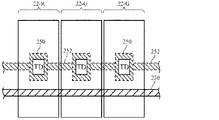
一実施形態によれば、底部導電性シールドを有するディスプレイピクセル22が提供される(例えば、図5を参照)。図5に示すように、薄膜駆動トランジスタTDなどの薄膜トランジスタ構造体は、ガラス、ポリイミド又は他の透明な誘電材料から作製された透明な基板200上に形成され得る。薄膜トランジスタTDは、図3に関して説明したディスプレイピクセル駆動トランジスタTDとして働き得る。
According to one embodiment, a
バッファ層306などの1つ以上のバッファ層が、基板200上に形成され得る。バッファ層306は、マルチバッファ(MB)層と称されることがある層、活性酸化物層、及び任意の好適な透明な誘電材料から形成される他の層を含み得る。
One or more buffer layers, such as buffer layer 306, may be formed on
トランジスタTDのための活物質208が、バッファ層202上に形成され得る。活物質208は、ポリシリコン、インジウムガリウム酸化亜鉛、アモルファスシリコン、又は他の半導体物質の層であり得る。ゲート絶縁層204などのゲート絶縁層が、バッファ層202上に、活物質を覆って形成され得る。ゲート絶縁体204は、シリコン酸化物などの誘電体から形成され得る。ゲート導体210など導電性ゲート構造体が、ゲート絶縁体204上に配設され得る。ゲート導体210は、薄膜トランジスタTDのためのゲート端子として働き得る。ゲート210の直ぐ下の活物質208の一部分は、トランジスタTDのためのチャネル領域として働き得る。
An active material 208 for the transistor TD may be formed on the
経路230などの導電経路は、トランジスタTDに直ぐ近くに形成され得る。経路230は、例えば、制御信号/データ信号のうちの1つをディスプレイピクセル22に伝達するための制御線の一部であり得る。1つの構成では、経路230は、信号SCAN1をピクセル22中の対応するスイッチSW1に伝えるための走査線の一部であり得る(図3)。別の構成では、経路230は、信号SCAN2をピクセル22中の対応するスイッチSW2に伝えるための走査線の一部であり得る。更に別の構成では、経路230は、信号EMをピクセル22中の対応するスイッチSW3に伝えるための走査線の一部であり得る。
A conductive path, such as
窒化ケイ素層などのパッシベーション層(図5には示されていない)が、任意選択的に、ゲート絶縁層204の上に、ゲート210を覆って形成され得る。パッシベーション層の堆積の後、薄膜トランジスタ構造体を不活性化するために、水素化アニーリングプロセスが適用され得る。
A passivation layer (not shown in FIG. 5), such as a silicon nitride layer, can optionally be formed over the
1つ以上の誘電体層212(層間絶縁(interlayer dielectric)層又は「ILD」層と称されることがある)が、薄膜トランジスタ構造体上に形成され得る。ゲート210及び経路230が形成される材料は、「M1」金属と称されることがある。したがって、M1金属が形成され誘電体層は、M1金属ルーティング層と称される。
One or more dielectric layers 212 (sometimes referred to as interlayer dielectric layers or “ILD” layers) may be formed on the thin film transistor structure. The material from which the
薄膜トランジスタTDなどの薄膜トランジスタ構造体は、発光ダイオード219のカソード220(例えば、酸化インジウムスズ又はインジウム酸化亜鉛などの透明導電層)とアノード216(例えば、光反射金属層)との間に電流を通すことができる。この電流が有機発光ダイオードの発光エレクトロルミネッセンス層(発光層)218を通過するにつれて、光が発生され得る。このようにして発生した光は、放出光に所望の色を与える対応するカラーフィルタ素子(図示せず)を通過し得る。一般に、ディスプレイ14のために、上面発光型ディスプレイピクセル又は底面発型光ディスプレイピクセル構成のいずれかが実装され得る。 A thin film transistor structure, such as thin film transistor TD, conducts current between the cathode 220 (eg, a transparent conductive layer such as indium tin oxide or indium zinc oxide) of the light emitting diode 219 and the anode 216 (eg, a light reflecting metal layer). Can do. As this current passes through the light emitting electroluminescent layer (light emitting layer) 218 of the organic light emitting diode, light can be generated. The light thus generated can pass through a corresponding color filter element (not shown) that gives the desired color to the emitted light. In general, either a top-emitting display pixel or a bottom-emitting light display pixel configuration can be implemented for the display 14.
上記で説明したように、点線の電界線232によって示されるように、トランジスタTDと経路230などの隣接する制御経路との間に電界が発生することがあり得る。本発明の一実施形態によれば、シールド250などの導電性シールド構造体が、バッファ層202内の駆動トランジスタTDの直ぐ下に形成され得る。シールド250は、活物質208及びゲート絶縁層204と直接接触すべきでない。シールド構造体250は、酸化インジウムスズ、モリブデン及びモリブデンタングステンなどの透明導電性材料、又はチタン、銅、アルミニウム若しくは他の金属などの不透明な導電性材料から形成され得る。このようにして形成されると、導電性底部シールド250は、トランジスタTDのための金属経路230又は任意の他の隣接する制御線から発生する任意の水平電界を遮断する機能を果たし得る(例えば、シールド250は、任意の望ましくない水平電界がトランジスタTDの動作に悪影響を及ぼすことを防止し得る)。したがって、このようにしてトランジスタTDの下に形成されたシールド250は、「底部」シールド又は電界シールドと称されることがある。
As described above, an electric field may be generated between the transistor TD and an adjacent control path, such as
一般に、各ピクセル中の駆動トランジスタの直ぐ下にのみ底部導電性シールドを形成することが望ましいことがある。換言すると、周辺のスイッチングトランジスタSW1、SW2及びSW3(図3)について、底部導電性シールドを形成する必要はない。駆動薄膜トランジスタTDの下のみにシールド250を形成することは、ピクセル22内の任意の望ましくない寄生容量を低減するのに役立ち得、それにより、動的な電力消費が最小限に抑えられる。
In general, it may be desirable to form a bottom conductive shield only directly below the drive transistor in each pixel. In other words, there is no need to form bottom conductive shields for the surrounding switching transistors SW1, SW2 and SW3 (FIG. 3). Forming the
図5の構造体は、特定の色の単一のサブピクセルを形成する。ディスプレイ14には、1つのディスプレイピクセル22に3つ若しくは4つのサブピクセルが、又は1つのディスプレイピクセル22に他の好適な数のサブピクセルがあり得る。図6は、3つのサブピクセル22−R、22−G及び22−Bを有する例示的なディスプレイピクセル22の図である。サブピクセル22−Rは、赤色光を表示するための回路を含み得る(例えば、サブピクセル22−Rは、赤色カラーフィルタ素子を通して光を射出する発光ダイオードを含み得る)。サブピクセル22−Gは、緑色光を表示するための回路を含み得る(例えば、サブピクセル22−Gは、緑色カラーフィルタ素子を通して光を射出する発光ダイオードを含み得る)。サブピクセル22−Bは、青色光を表示するための回路を含み得る(例えば、サブピクセル22−Bは、青色カラーフィルタ素子を通して光を射出する発光ダイオードを含み得る)。これは単なる例示である。一般に、ディスプレイピクセル22は、可視スペクトルの赤色光、緑色光、青色光、シアン光、マゼンタ光、黄色光、白色光及び/又は他の種類の光を透過するように構成された任意の数のサブピクセルを含み得る。
The structure of FIG. 5 forms a single subpixel of a particular color. The display 14 may have three or four subpixels in one
図6に示すように、サブピクセルのそれぞれは、駆動トランジスタTDと、駆動トランジスタTDの占有面積と直接重なる対応する導電性光シールド250とを含む。このようにして構成すると、光シールド構造体250は、制御経路230にバイアス電圧が印加された結果として発生する任意の電界が駆動トランジスタの動作と干渉することを防止する機能を果たす。底部シールド250が、電気的に浮遊している(即ち、シールド250が、任意のプルアップ回路又はプルダウン回路によりアクティブには駆動されず、互いに接続されてない)図6の例は、単なる例示である。他の好適な構成では、導電性短絡経路252を使用して、底部シールド250が短絡し得る(例えば、図7を参照)。
As shown in FIG. 6, each of the sub-pixels includes a drive transistor TD and a corresponding conductive
図7に示すように、導電性短絡経路252は、導電性シールド250と同じ層中に形成され得る(例えば、図5のバッファ層202に導電性短絡経路252を形成することができる)。また、導電性短絡経路252は、シールド250と同じ材料から形成され得る(例えば、短絡経路252は、酸化インジウムスズ、モリブデン及びモリブデンタングステンなどの透明な導電性材料、又はチタン、銅、アルミニウム若しくは他の金属などの不透明な導電性材料から形成され得る)。導電経路252を介して底部シールドを一緒に短絡させると、特に経路252が何らかの電源供給ラインに短絡した時に、シールド能力を改善することができる。
As shown in FIG. 7, the conductive
図8は、ディスプレイ14においてピクセル22のアレイを示す図である。図8に示すように、底部シールド250(例えば、導電性シールド250−R、250−G及び250−B)の少なくとも一部分を、経路252を介して電源供給ライン254(例えば、アース電源電圧VSSELが提供される電源供給ライン)に短絡させることができる。底部シールド短絡経路252は、ディスプレイ14の外周においてのみアース線254に結合され得る。このようにして接続すると、各ディスプレイサブピクセル中の底部シールドは定常電圧VSSELに駆動され、それにより、駆動トランジスタがディスプレイピクセルアレイ全体にわたってより一貫した様式で動作することが可能になる。
FIG. 8 is a diagram illustrating an array of
更に図8を参照すると、少なくともいくつかディスプレイピクセル22中の底部シールドが、浮遊しており、電源供給ライン254に接続されていない。これは単なる例示である。別の例として、ピクセルアレイ全体における各サブピクセルの導電性シールド250は、電気的に浮遊していてもよい。更に別の例として、ピクセルアレイ全体における各サブピクセルの導電性シールド250を全て、アース電源供給ライン、正電源供給ライン又は他の電源供給ラインに短絡させてもよい。
Still referring to FIG. 8, at least some of the bottom shields in the
図5に関して上記で説明したように、底部シールド構造体250は、バッファ層202中に形成され得る。底部シールド構造体250がアース線(例えば、共通カソード電極)に短絡している構成では、底部シールド構造体を、薄膜トランジスタ層を貫通して形成された導電性スルーホール又は「ビア」構造を介してカソードに結合することができる。
As described above with respect to FIG. 5, the
どのように底部シールド構造体をカソード電極に短絡させることができるかを示す、ディスプレイ14の周辺部分260の側断面図が図9に示されている。図9に示すように、導電性短絡経路252は、バッファ層202中に形成され、ディスプレイ14の外周へと延び得る。金属構造231などの1つ以上のM1金属ルーティング経路が、ゲート絶縁層204上に形成され得る。底部導電経路252との接触を形成するために、層212及び204を貫通して第1のビア構造290が形成され得る。詳細には、ビア290は、経路252とアノード216との間に電気的接続を確立し得る。アノード216との接触を形成するために、層218を貫通して第2のビア構造292が形成され得る。詳細には、ビア282は、アノード216とカソード220との間に電気的接続を確立し得る。このようにして構成すると、図5、図7及び図8に示した種類の底部シールド構造体250は、導電経路252並びにビア290及び292を経由してアースカソード電極に短絡し得る。
A side cross-sectional view of the
一実施形態によれば、基板と、基板上に形成された薄膜トランジスタと、薄膜トランジスタと基板との間に介挿された少なくとも1つのバッファ層と、バッファ層中の薄膜トランジスタの直ぐ下に形成された導電性シールド構造体と含むディスプレイが提供される。 According to one embodiment, a substrate, a thin film transistor formed on the substrate, at least one buffer layer interposed between the thin film transistor and the substrate, and a conductive material formed immediately below the thin film transistor in the buffer layer. A display including a conductive shield structure is provided.
別の実施形態によれば、導電性シールド構造体は、透明な導電材料から形成される。 According to another embodiment, the conductive shield structure is formed from a transparent conductive material.
別の実施形態によれば、導電性シールド構造体は、不透明導電材料から形成される。 According to another embodiment, the conductive shield structure is formed from an opaque conductive material.
別の実施形態によれば、導電性シールド構造体は、電気的に浮遊している。 According to another embodiment, the conductive shield structure is electrically floating.
別の実施形態によれば、ディスプレイが電力供給ラインを含み、導電性シールド構造体は、電力供給ラインに短絡している。 According to another embodiment, the display includes a power supply line, and the conductive shield structure is shorted to the power supply line.
別の実施形態によれば、ディスプレイは、ビアを貫通して導電性シールド構造体に短絡しているカソード電極を含む。 According to another embodiment, the display includes a cathode electrode that is shorted to the conductive shield structure through the via.
別の実施形態によれば、薄膜トランジスタは、ゲート絶縁層上に形成されたゲートを有し、導電性シールド構造体は、ゲート絶縁層と直接接触していない。 According to another embodiment, the thin film transistor has a gate formed on the gate insulating layer, and the conductive shield structure is not in direct contact with the gate insulating layer.
別の実施形態によれば、本ディスプレイは、追加の薄膜トランジスタであって、導電性シールド構造体が、前薄膜トランジスタの下にのみ形成され、追加の薄膜トランジスタの下には形成されない、追加の薄膜トランジスタを含む。 According to another embodiment, the display includes an additional thin film transistor, wherein the conductive shield structure is formed only under the previous thin film transistor and not under the additional thin film transistor. .
一実施形態によれば、基板上の薄膜トランジスタを形成することと、薄膜トランジスタと基板との間に介挿されたバッファ層を形成することと、薄膜トランジスタのために、バッファ層中に導電性シールド構造体を形成することとを含むディスプレイピクセルを製造する方法が提供される。 According to one embodiment, forming a thin film transistor on a substrate, forming a buffer layer interposed between the thin film transistor and the substrate, and a conductive shield structure in the buffer layer for the thin film transistor Forming a display pixel is provided.
別の実施形態によれば、電界シールドを形成することは、薄膜トランジスタの直ぐ下に導電性シールド構造体を形成することを含む。 According to another embodiment, forming the electric field shield includes forming a conductive shield structure directly under the thin film transistor.
別の実施形態によれば、本方法は、薄膜トランジスタに結合された発光ダイオードを形成することを含む。 According to another embodiment, the method includes forming a light emitting diode coupled to the thin film transistor.
別の実施形態によれば、発光ダイオードは、カソード電極を有し、本方法は、導電性ビア構造を貫通してカソード電極に電界シールドを短絡させることを含む。 According to another embodiment, the light emitting diode has a cathode electrode and the method includes shorting an electric field shield to the cathode electrode through the conductive via structure.
別の実施形態によれば、電界シールドは、アクティブには駆動されない。 According to another embodiment, the electric field shield is not actively driven.
別の実施形態によれば、本方法は、基板上に追加の薄膜トランジスタを形成することと、追加の薄膜トランジスタのためにバッファ層中に追加の電界シールドを形成することとを含む。 According to another embodiment, the method includes forming an additional thin film transistor on the substrate and forming an additional electric field shield in the buffer layer for the additional thin film transistor.
別の実施形態によれば、本方法は、バッファ層中に、電界シールドと追加の電界シールドとを短絡させる導電経路を形成することを含む。 According to another embodiment, the method includes forming a conductive path in the buffer layer that shorts the electric field shield and the additional electric field shield.
一実施形態によれば、アレイで配列されるディスプレイピクセルを備え、アレイ中の各ディスプレイピクセルが、駆動トランジスタと、駆動トランジスタの下に形成された導電性シールドと、を含む、電子機器が提供される。 According to one embodiment, there is provided an electronic device comprising display pixels arranged in an array, wherein each display pixel in the array includes a drive transistor and a conductive shield formed under the drive transistor. The
別の実施形態によれば、アレイ中の各ディスプレイピクセルは駆動トランジスタに結合された発光ダイオードを更に含む。 According to another embodiment, each display pixel in the array further includes a light emitting diode coupled to the drive transistor.
別の実施形態によれば、アレイ中の各ディスプレイピクセルの導電性シールドは、電気的に浮遊している。 According to another embodiment, the conductive shield of each display pixel in the array is electrically floating.
別の実施形態によれば、アレイ中の各ディスプレイピクセルの導電性シールドは、共通電極に短絡している。 According to another embodiment, the conductive shield of each display pixel in the array is shorted to the common electrode.
別の実施形態によれば、アレイの第1の部分中の各ディスプレイピクセルの導電性シールドは、電気的に浮遊しており、アレイの第2の部分中の各ディスプレイピクセルの導電性シールドは、共通の電極に短絡している。 According to another embodiment, the conductive shield of each display pixel in the first portion of the array is electrically floating and the conductive shield of each display pixel in the second portion of the array is Shorted to a common electrode.
上述の内容は単なる例示にすぎず、説明された実施形態の範囲及び趣旨から逸脱することなく、当業者によってさまざまな修正を行うことができる。前述の実施形態は、個々に又は任意の組み合わせで実行することができる。 The foregoing is merely exemplary and various modifications can be made by those skilled in the art without departing from the scope and spirit of the described embodiments. The foregoing embodiments can be performed individually or in any combination.
Claims (8)
前記基板上に形成された薄膜トランジスタと、
前記薄膜トランジスタと前記基板との間に介挿された少なくとも1つのバッファ層と、 前記バッファ層において前記薄膜トランジスタの直ぐ下に形成された導電性シールド構造体と、
電源供給ラインと、
を備え、
前記導電性シールド構造体が、透明な導電材料から形成され、
前記導電性シールド構造体が、前記電源供給ラインに短絡していることを特徴とする、ディスプレイ。 A substrate,
A thin film transistor formed on the substrate;
At least one buffer layer interposed between the thin film transistor and the substrate; and a conductive shield structure formed immediately below the thin film transistor in the buffer layer;
A power supply line;
With
The conductive shield structure is formed of a transparent conductive material;
The display according to claim 1, wherein the conductive shield structure is short-circuited to the power supply line.
基板上に薄膜トランジスタを形成することと、
前記薄膜トランジスタと前記基板との間に介挿されたバッファ層であって、第1の面及び対向する第2の面を有する前記バッファ層を形成することと、
前記薄膜トランジスタのために前記バッファ層中に電界シールドを形成することであって、前記バッファ層の前記第1の面及び対向する第2の面の間に前記電界シールドが介挿され、
前記薄膜トランジスタに結合された発光ダイオードを形成することであって、前記発光ダイオードがカソード電極を有し、
導電性ビア構造を介して前記電界シールドを前記カソード電極に短絡させることと、
を含む、ディスプレイピクセルの製造方法。 A display manufacturing method comprising:
Forming a thin film transistor on a substrate;
Forming a buffer layer interposed between the thin film transistor and the substrate, the buffer layer having a first surface and an opposing second surface;
Forming an electric field shield in the buffer layer for the thin film transistor, the electric field shield being interposed between the first surface and the opposing second surface of the buffer layer;
Forming a light emitting diode coupled to the thin film transistor, the light emitting diode having a cathode electrode;
Shorting the electric field shield to the cathode electrode via a conductive via structure;
A method for manufacturing a display pixel , comprising:
前記基板上に、前記ディスプレイの第2サブピクセルに関する追加の駆動トランジスタを形成することと、
前記追加の駆動トランジスタのために前記バッファ層中に追加の電界シールドを形成することと、
を更に含む、請求項3に記載の方法。 The thin film transistor is a driving transistor for a first subpixel of the display, and the method comprises:
Forming an additional drive transistor on the substrate for the second sub-pixel of the display ;
Forming an additional electric field shield in the buffer layer for the additional drive transistor;
The method of claim 3 , further comprising:
アレイで配列されるディスプレイピクセルを備え、前記アレイ中の各ディスプレイピクセルが、
駆動トランジスタと、
前記駆動トランジスタの下に形成された透明な導電性シールドと、
ビアを介して前記透明な導電性シールドに短絡しているカソード電極を有する発光ダイオードと、
含み、
前記ディスプレイピクセルに信号を送る導電経路を更に備え、前記透明な導電性シールドは、前記アレイにおける少なくとも1つの前記ディスプレイピクセル中の前記導電経路により生成された電界から前記駆動トランジスタをブロックする、
電子機器ディスプレイ。 An electronic device display,
Comprising display pixels arranged in an array, wherein each display pixel in the array comprises:
A driving transistor;
A transparent conductive shield formed under the driving transistor;
A light emitting diode having a cathode electrode shorted to the transparent conductive shield via a via;
Including
Further comprising a conductive path for sending a signal to the display pixel, wherein the transparent conductive shield blocks the drive transistor from an electric field generated by the conductive path in at least one of the display pixels in the array;
Electronic device display.
Applications Claiming Priority (5)
| Application Number | Priority Date | Filing Date | Title |
|---|---|---|---|
| US201461929907P | 2014-01-21 | 2014-01-21 | |
| US61/929,907 | 2014-01-21 | ||
| US14/488,725 US9337247B2 (en) | 2014-01-21 | 2014-09-17 | Organic light-emitting diode display with bottom shields |
| US14/488,725 | 2014-09-17 | ||
| PCT/US2014/057061 WO2015112203A1 (en) | 2014-01-21 | 2014-09-23 | Organic light-emitting diode display with bottom shields |
Publications (2)
| Publication Number | Publication Date |
|---|---|
| JP2017505457A JP2017505457A (en) | 2017-02-16 |
| JP6623164B2 true JP6623164B2 (en) | 2019-12-18 |
Family
ID=53545529
Family Applications (1)
| Application Number | Title | Priority Date | Filing Date |
|---|---|---|---|
| JP2016545830A Active JP6623164B2 (en) | 2014-01-21 | 2014-09-23 | Organic light emitting diode display with bottom shield |
Country Status (6)
| Country | Link |
|---|---|
| US (1) | US9337247B2 (en) |
| EP (2) | EP4236656A3 (en) |
| JP (1) | JP6623164B2 (en) |
| KR (1) | KR101869625B1 (en) |
| AU (1) | AU2014379553C1 (en) |
| WO (1) | WO2015112203A1 (en) |
Families Citing this family (24)
| Publication number | Priority date | Publication date | Assignee | Title |
|---|---|---|---|---|
| US9472605B2 (en) * | 2014-11-17 | 2016-10-18 | Apple Inc. | Organic light-emitting diode display with enhanced aperture ratio |
| US10128317B2 (en) * | 2014-12-22 | 2018-11-13 | Emagin Corporation | Method for eliminating electrical cross-talk in OLED microdisplays |
| KR102325191B1 (en) * | 2015-01-05 | 2021-11-10 | 삼성디스플레이 주식회사 | Display Device |
| KR102397799B1 (en) * | 2015-06-30 | 2022-05-16 | 엘지디스플레이 주식회사 | Thin Film Transistor And Display Device Comprising The Same |
| JP6654466B2 (en) * | 2015-08-31 | 2020-02-26 | 株式会社Joled | Semiconductor device, display device, method of manufacturing display device, and electronic apparatus |
| US9935165B2 (en) * | 2015-08-31 | 2018-04-03 | Joled, Inc. | Semiconductor device, display unit, method of manufacturing display unit, and electronic apparatus |
| KR102628884B1 (en) * | 2015-11-27 | 2024-01-26 | 엘지디스플레이 주식회사 | Organic light emitting display device |
| CN113299719A (en) * | 2016-01-21 | 2021-08-24 | 苹果公司 | Power and data routing structure for organic light emitting diode display |
| JP2017207744A (en) * | 2016-05-11 | 2017-11-24 | 株式会社半導体エネルギー研究所 | Display device, module, and electronic device |
| JP6813967B2 (en) * | 2016-06-30 | 2021-01-13 | 株式会社ジャパンディスプレイ | Display device with input function |
| KR102693312B1 (en) * | 2016-09-30 | 2024-08-07 | 엘지디스플레이 주식회사 | Organic light emitting display device and method of manufacturing the same |
| KR102613853B1 (en) * | 2016-12-19 | 2023-12-18 | 엘지디스플레이 주식회사 | Organic light emitting display device |
| CN107436685B (en) * | 2017-07-31 | 2020-07-07 | 京东方科技集团股份有限公司 | Display device, self-luminous display panel and gesture recognition method |
| CN207781601U (en) * | 2017-12-14 | 2018-08-28 | 京东方科技集团股份有限公司 | Display device |
| WO2019139610A1 (en) * | 2018-01-12 | 2019-07-18 | Intel Corporation | Shield structure for a group iii-nitride device and method of fabrication |
| JP7085352B2 (en) * | 2018-01-15 | 2022-06-16 | 株式会社ジャパンディスプレイ | Display device |
| JP7127802B2 (en) * | 2018-04-18 | 2022-08-30 | 三国電子有限会社 | Display device with touch detection function and manufacturing method thereof |
| CN208622728U (en) * | 2018-09-07 | 2019-03-19 | 京东方科技集团股份有限公司 | A kind of array substrate, display panel and display device |
| KR102531674B1 (en) | 2018-12-31 | 2023-05-12 | 삼성디스플레이 주식회사 | Display panel |
| KR102690931B1 (en) * | 2019-01-17 | 2024-08-01 | 삼성디스플레이 주식회사 | Display device including the same, and method for manufacturing the same |
| KR20210104221A (en) | 2020-02-14 | 2021-08-25 | 삼성디스플레이 주식회사 | Display panel and electric apparatus including the same |
| EP3933931A1 (en) * | 2020-07-02 | 2022-01-05 | LG Display Co., Ltd. | Display panel and method of fabricating the same |
| EP4229622A1 (en) * | 2020-12-09 | 2023-08-23 | Apple Inc. | Displays with reduced temperature luminance sensitivity |
| US11532282B2 (en) | 2020-12-09 | 2022-12-20 | Apple Inc. | Displays with reduced temperature luminance sensitivity |
Family Cites Families (38)
| Publication number | Priority date | Publication date | Assignee | Title |
|---|---|---|---|---|
| TW353150B (en) * | 1994-05-13 | 1999-02-21 | Thomson Consumer Electronics | Liquid crystal display device |
| JP3276930B2 (en) * | 1998-11-17 | 2002-04-22 | 科学技術振興事業団 | Transistor and semiconductor device |
| US6674136B1 (en) * | 1999-03-04 | 2004-01-06 | Semiconductor Energy Laboratory Co., Ltd. | Semiconductor device having driver circuit and pixel section provided over same substrate |
| JP2001148480A (en) * | 1999-11-18 | 2001-05-29 | Nec Corp | Thin film transistor and device and method for manufacturing the same |
| JP4831862B2 (en) * | 1999-11-30 | 2011-12-07 | 株式会社半導体エネルギー研究所 | Electronic equipment |
| JP4896314B2 (en) * | 2000-08-04 | 2012-03-14 | 株式会社半導体エネルギー研究所 | Display device |
| US6825496B2 (en) * | 2001-01-17 | 2004-11-30 | Semiconductor Energy Laboratory Co., Ltd. | Light emitting device |
| JP2002323706A (en) | 2001-02-23 | 2002-11-08 | Nec Corp | Active matrix liquid crystal display device of transverse electric field system and method for manufacturing the same |
| US7474002B2 (en) * | 2001-10-30 | 2009-01-06 | Semiconductor Energy Laboratory Co., Ltd. | Semiconductor device having dielectric film having aperture portion |
| JP2003297851A (en) * | 2002-01-30 | 2003-10-17 | Sanyo Electric Co Ltd | Semiconductor display and manufacturing method therefor |
| KR100896167B1 (en) | 2002-04-24 | 2009-05-11 | 이 잉크 코포레이션 | Electronic displays |
| JP4438312B2 (en) * | 2002-05-21 | 2010-03-24 | セイコーエプソン株式会社 | Electro-optical device and electronic apparatus |
| JP2005158493A (en) * | 2003-11-26 | 2005-06-16 | Seiko Epson Corp | Organic electroluminescence device and electronic equipment |
| KR100563060B1 (en) * | 2004-01-16 | 2006-03-24 | 삼성에스디아이 주식회사 | Flat panel display with TFT |
| JP4507611B2 (en) * | 2004-01-29 | 2010-07-21 | セイコーエプソン株式会社 | ORGANIC ELECTROLUMINESCENCE DEVICE AND ELECTRONIC DEVICE |
| JP4196906B2 (en) | 2004-09-02 | 2008-12-17 | セイコーエプソン株式会社 | Liquid crystal display device and electronic device |
| JP4942341B2 (en) * | 2004-12-24 | 2012-05-30 | 三洋電機株式会社 | Display device |
| KR100793357B1 (en) * | 2005-03-18 | 2008-01-11 | 삼성에스디아이 주식회사 | Thin Film Transitor and Flat Panel Display Device, and Method of fabricating thereof |
| TWI280073B (en) * | 2005-09-15 | 2007-04-21 | Au Optronics Corp | Organic light emitting diode display panel |
| JP2007114726A (en) * | 2005-09-26 | 2007-05-10 | Sanyo Electric Co Ltd | Organic electroluminescence display device |
| KR101242030B1 (en) * | 2006-06-22 | 2013-03-11 | 엘지디스플레이 주식회사 | Organic Electroluminescent Device |
| TWI303888B (en) * | 2006-07-21 | 2008-12-01 | Au Optronics Corp | Ltps-lcd structure and method for manufacturing the same |
| JP4179393B2 (en) * | 2006-09-14 | 2008-11-12 | エプソンイメージングデバイス株式会社 | Display device and manufacturing method thereof |
| US8133773B2 (en) | 2007-10-17 | 2012-03-13 | Au Optronics Corporation | Apparatus and method for reducing photo leakage current for TFT LCD |
| TWI324832B (en) * | 2007-10-23 | 2010-05-11 | Au Optronics Corp | Photo sensor and fabrication method thereof |
| JP5486784B2 (en) | 2008-09-11 | 2014-05-07 | 株式会社ジャパンディスプレイ | Liquid crystal display |
| WO2010111306A1 (en) * | 2009-03-25 | 2010-09-30 | Qualcomm Mems Technologies, Inc. | Em shielding for display devices |
| RU2511709C2 (en) | 2009-06-30 | 2014-04-10 | Шарп Кабусики Кайся | Liquid crystal display device |
| US9059294B2 (en) * | 2010-01-07 | 2015-06-16 | Sharp Kabushiki Kaisha | Semiconductor device, active matrix substrate, and display device |
| KR20110111708A (en) * | 2010-04-05 | 2011-10-12 | 삼성모바일디스플레이주식회사 | Display device and method of manufacturing the same |
| KR101343293B1 (en) * | 2010-04-30 | 2013-12-18 | 샤프 가부시키가이샤 | Circuit board and display device |
| KR102479939B1 (en) * | 2010-07-02 | 2022-12-20 | 가부시키가이샤 한도오따이 에네루기 켄큐쇼 | Semiconductor device and manufacturing method thereof |
| JP2012064604A (en) * | 2010-09-14 | 2012-03-29 | Casio Comput Co Ltd | Transistor structure, method of manufacturing transistor structure, and light-emitting device |
| KR101944704B1 (en) * | 2012-03-02 | 2019-04-17 | 엘지디스플레이 주식회사 | Liquid crystal display device |
| US9869908B2 (en) | 2012-03-06 | 2018-01-16 | Apple Inc. | Pixel inversion artifact reduction |
| JPWO2013171938A1 (en) * | 2012-05-16 | 2016-01-07 | 株式会社Joled | Display device |
| KR101915755B1 (en) | 2012-05-22 | 2018-11-07 | 삼성디스플레이 주식회사 | Organic light-emitting display apparatus and manufacturing method thereof |
| KR101936773B1 (en) | 2012-07-03 | 2019-01-09 | 엘지디스플레이 주식회사 | Method for manufacturing liquid crystal display device |
-
2014
- 2014-09-17 US US14/488,725 patent/US9337247B2/en active Active
- 2014-09-23 KR KR1020167019387A patent/KR101869625B1/en active IP Right Grant
- 2014-09-23 AU AU2014379553A patent/AU2014379553C1/en active Active
- 2014-09-23 JP JP2016545830A patent/JP6623164B2/en active Active
- 2014-09-23 EP EP23180473.3A patent/EP4236656A3/en active Pending
- 2014-09-23 EP EP14879712.9A patent/EP3097594B1/en active Active
- 2014-09-23 WO PCT/US2014/057061 patent/WO2015112203A1/en active Application Filing
Also Published As
| Publication number | Publication date |
|---|---|
| US9337247B2 (en) | 2016-05-10 |
| EP3097594A4 (en) | 2017-06-07 |
| AU2014379553C1 (en) | 2018-04-05 |
| KR101869625B1 (en) | 2018-06-20 |
| US20150206931A1 (en) | 2015-07-23 |
| KR20160101097A (en) | 2016-08-24 |
| EP4236656A3 (en) | 2023-11-01 |
| AU2014379553B2 (en) | 2017-09-28 |
| EP3097594A1 (en) | 2016-11-30 |
| EP3097594B1 (en) | 2023-06-28 |
| EP4236656A2 (en) | 2023-08-30 |
| AU2014379553A1 (en) | 2016-07-07 |
| JP2017505457A (en) | 2017-02-16 |
| WO2015112203A1 (en) | 2015-07-30 |
Similar Documents
| Publication | Publication Date | Title |
|---|---|---|
| JP6623164B2 (en) | Organic light emitting diode display with bottom shield | |
| US9716134B2 (en) | Organic light-emitting diode display with bottom shields | |
| US9847051B2 (en) | Organic light-emitting diode display with minimized subpixel crosstalk | |
| US9397124B2 (en) | Organic light-emitting diode display with double gate transistors | |
| JP6457086B2 (en) | Organic light-emitting diode display with large aperture ratio | |
| US20230035245A1 (en) | Electronic Display with In-Pixel Compensation and Oxide Drive Transistors | |
| US20210280130A1 (en) | Display device | |
| US9336709B2 (en) | Displays with overlapping light-emitting diodes and gate drivers | |
| US9647048B2 (en) | Capacitor structures for display pixel threshold voltage compensation circuits | |
| KR20160092530A (en) | Organic light emitting display device | |
| CN204204377U (en) | Display and electronic equipment display | |
| KR20160105956A (en) | Organic light emitting display device | |
| EP3023970A2 (en) | Display panel for compensating negative power supply voltage, display module and mobile device including the same | |
| JP7546169B2 (en) | Display with reduced temperature and brightness sensitivity - Patents.com | |
| CN110783345A (en) | Display device | |
| JP2023517218A (en) | Large panel display with reduced routing line resistance | |
| KR102510401B1 (en) | Display device and method for manufacturing the same |
Legal Events
| Date | Code | Title | Description |
|---|---|---|---|
| A621 | Written request for application examination |
Free format text: JAPANESE INTERMEDIATE CODE: A621 Effective date: 20160712 |
|
| A131 | Notification of reasons for refusal |
Free format text: JAPANESE INTERMEDIATE CODE: A131 Effective date: 20170522 |
|
| A977 | Report on retrieval |
Free format text: JAPANESE INTERMEDIATE CODE: A971007 Effective date: 20170517 |
|
| A521 | Request for written amendment filed |
Free format text: JAPANESE INTERMEDIATE CODE: A523 Effective date: 20170821 |
|
| A02 | Decision of refusal |
Free format text: JAPANESE INTERMEDIATE CODE: A02 Effective date: 20180205 |
|
| A521 | Request for written amendment filed |
Free format text: JAPANESE INTERMEDIATE CODE: A523 Effective date: 20180529 |
|
| A911 | Transfer to examiner for re-examination before appeal (zenchi) |
Free format text: JAPANESE INTERMEDIATE CODE: A911 Effective date: 20180605 |
|
| A912 | Re-examination (zenchi) completed and case transferred to appeal board |
Free format text: JAPANESE INTERMEDIATE CODE: A912 Effective date: 20180629 |
|
| A521 | Request for written amendment filed |
Free format text: JAPANESE INTERMEDIATE CODE: A523 Effective date: 20190903 |
|
| A61 | First payment of annual fees (during grant procedure) |
Free format text: JAPANESE INTERMEDIATE CODE: A61 Effective date: 20191125 |
|
| R150 | Certificate of patent or registration of utility model |
Ref document number: 6623164 Country of ref document: JP Free format text: JAPANESE INTERMEDIATE CODE: R150 |
|
| R250 | Receipt of annual fees |
Free format text: JAPANESE INTERMEDIATE CODE: R250 |
|
| R250 | Receipt of annual fees |
Free format text: JAPANESE INTERMEDIATE CODE: R250 |