JP4896314B2 - Display device - Google Patents
Display device Download PDFInfo
- Publication number
- JP4896314B2 JP4896314B2 JP2001235469A JP2001235469A JP4896314B2 JP 4896314 B2 JP4896314 B2 JP 4896314B2 JP 2001235469 A JP2001235469 A JP 2001235469A JP 2001235469 A JP2001235469 A JP 2001235469A JP 4896314 B2 JP4896314 B2 JP 4896314B2
- Authority
- JP
- Japan
- Prior art keywords
- film
- light
- insulating film
- shielding film
- region
- Prior art date
- Legal status (The legal status is an assumption and is not a legal conclusion. Google has not performed a legal analysis and makes no representation as to the accuracy of the status listed.)
- Expired - Fee Related
Links
- 239000003990 capacitor Substances 0.000 claims description 45
- 239000004065 semiconductor Substances 0.000 claims description 20
- 230000015572 biosynthetic process Effects 0.000 claims description 10
- 239000010408 film Substances 0.000 description 227
- 239000010410 layer Substances 0.000 description 43
- 239000000758 substrate Substances 0.000 description 40
- 238000000034 method Methods 0.000 description 33
- 239000011159 matrix material Substances 0.000 description 32
- 239000004973 liquid crystal related substance Substances 0.000 description 31
- 238000003860 storage Methods 0.000 description 27
- 239000012535 impurity Substances 0.000 description 22
- 239000000463 material Substances 0.000 description 18
- OAICVXFJPJFONN-UHFFFAOYSA-N Phosphorus Chemical compound [P] OAICVXFJPJFONN-UHFFFAOYSA-N 0.000 description 14
- 229910052698 phosphorus Inorganic materials 0.000 description 14
- 239000011574 phosphorus Substances 0.000 description 14
- 229910052581 Si3N4 Inorganic materials 0.000 description 12
- 125000004429 atom Chemical group 0.000 description 12
- 230000008569 process Effects 0.000 description 12
- HQVNEWCFYHHQES-UHFFFAOYSA-N silicon nitride Chemical compound N12[Si]34N5[Si]62N3[Si]51N64 HQVNEWCFYHHQES-UHFFFAOYSA-N 0.000 description 12
- 229910021417 amorphous silicon Inorganic materials 0.000 description 11
- 238000000137 annealing Methods 0.000 description 11
- 239000011521 glass Substances 0.000 description 11
- 238000010438 heat treatment Methods 0.000 description 11
- VYPSYNLAJGMNEJ-UHFFFAOYSA-N silicon dioxide Inorganic materials O=[Si]=O VYPSYNLAJGMNEJ-UHFFFAOYSA-N 0.000 description 11
- 229910021419 crystalline silicon Inorganic materials 0.000 description 10
- 238000002425 crystallisation Methods 0.000 description 9
- 238000010586 diagram Methods 0.000 description 9
- 239000001257 hydrogen Substances 0.000 description 9
- 229910052739 hydrogen Inorganic materials 0.000 description 9
- 239000010936 titanium Substances 0.000 description 9
- ZOXJGFHDIHLPTG-UHFFFAOYSA-N Boron Chemical compound [B] ZOXJGFHDIHLPTG-UHFFFAOYSA-N 0.000 description 8
- UFHFLCQGNIYNRP-UHFFFAOYSA-N Hydrogen Chemical compound [H][H] UFHFLCQGNIYNRP-UHFFFAOYSA-N 0.000 description 8
- XUIMIQQOPSSXEZ-UHFFFAOYSA-N Silicon Chemical compound [Si] XUIMIQQOPSSXEZ-UHFFFAOYSA-N 0.000 description 8
- 229910052796 boron Inorganic materials 0.000 description 8
- 230000008025 crystallization Effects 0.000 description 8
- 238000004519 manufacturing process Methods 0.000 description 8
- 229920005989 resin Polymers 0.000 description 8
- 239000011347 resin Substances 0.000 description 8
- 229910052710 silicon Inorganic materials 0.000 description 8
- 239000010703 silicon Substances 0.000 description 8
- 229910052814 silicon oxide Inorganic materials 0.000 description 8
- 230000000694 effects Effects 0.000 description 7
- 125000006850 spacer group Chemical group 0.000 description 7
- IJGRMHOSHXDMSA-UHFFFAOYSA-N Atomic nitrogen Chemical compound N#N IJGRMHOSHXDMSA-UHFFFAOYSA-N 0.000 description 6
- PXHVJJICTQNCMI-UHFFFAOYSA-N Nickel Chemical compound [Ni] PXHVJJICTQNCMI-UHFFFAOYSA-N 0.000 description 6
- 239000011651 chromium Substances 0.000 description 6
- 229920001721 polyimide Polymers 0.000 description 6
- 239000000945 filler Substances 0.000 description 5
- 239000007789 gas Substances 0.000 description 5
- 238000002161 passivation Methods 0.000 description 5
- 230000001681 protective effect Effects 0.000 description 5
- 239000000565 sealant Substances 0.000 description 5
- XYFCBTPGUUZFHI-UHFFFAOYSA-N Phosphine Chemical compound P XYFCBTPGUUZFHI-UHFFFAOYSA-N 0.000 description 4
- 239000004642 Polyimide Substances 0.000 description 4
- NIXOWILDQLNWCW-UHFFFAOYSA-N acrylic acid group Chemical group C(C=C)(=O)O NIXOWILDQLNWCW-UHFFFAOYSA-N 0.000 description 4
- QVQLCTNNEUAWMS-UHFFFAOYSA-N barium oxide Chemical compound [Ba]=O QVQLCTNNEUAWMS-UHFFFAOYSA-N 0.000 description 4
- 239000003054 catalyst Substances 0.000 description 4
- 238000005984 hydrogenation reaction Methods 0.000 description 4
- 238000005224 laser annealing Methods 0.000 description 4
- 230000014759 maintenance of location Effects 0.000 description 4
- 229910052751 metal Inorganic materials 0.000 description 4
- 239000002184 metal Substances 0.000 description 4
- 150000002894 organic compounds Chemical class 0.000 description 4
- 230000010355 oscillation Effects 0.000 description 4
- 229910052760 oxygen Inorganic materials 0.000 description 4
- 239000003566 sealing material Substances 0.000 description 4
- 229910052715 tantalum Inorganic materials 0.000 description 4
- GUVRBAGPIYLISA-UHFFFAOYSA-N tantalum atom Chemical compound [Ta] GUVRBAGPIYLISA-UHFFFAOYSA-N 0.000 description 4
- WFKWXMTUELFFGS-UHFFFAOYSA-N tungsten Chemical compound [W] WFKWXMTUELFFGS-UHFFFAOYSA-N 0.000 description 4
- 229910052721 tungsten Inorganic materials 0.000 description 4
- 239000010937 tungsten Substances 0.000 description 4
- WQJQOUPTWCFRMM-UHFFFAOYSA-N tungsten disilicide Chemical compound [Si]#[W]#[Si] WQJQOUPTWCFRMM-UHFFFAOYSA-N 0.000 description 4
- VYZAMTAEIAYCRO-UHFFFAOYSA-N Chromium Chemical compound [Cr] VYZAMTAEIAYCRO-UHFFFAOYSA-N 0.000 description 3
- ZOKXTWBITQBERF-UHFFFAOYSA-N Molybdenum Chemical compound [Mo] ZOKXTWBITQBERF-UHFFFAOYSA-N 0.000 description 3
- RTAQQCXQSZGOHL-UHFFFAOYSA-N Titanium Chemical compound [Ti] RTAQQCXQSZGOHL-UHFFFAOYSA-N 0.000 description 3
- 229910045601 alloy Inorganic materials 0.000 description 3
- 239000000956 alloy Substances 0.000 description 3
- 229910052782 aluminium Inorganic materials 0.000 description 3
- XAGFODPZIPBFFR-UHFFFAOYSA-N aluminium Chemical compound [Al] XAGFODPZIPBFFR-UHFFFAOYSA-N 0.000 description 3
- 239000012298 atmosphere Substances 0.000 description 3
- QVGXLLKOCUKJST-UHFFFAOYSA-N atomic oxygen Chemical compound [O] QVGXLLKOCUKJST-UHFFFAOYSA-N 0.000 description 3
- 230000003197 catalytic effect Effects 0.000 description 3
- 229910052804 chromium Inorganic materials 0.000 description 3
- 150000001875 compounds Chemical class 0.000 description 3
- 238000005468 ion implantation Methods 0.000 description 3
- 150000002500 ions Chemical class 0.000 description 3
- 229910052750 molybdenum Inorganic materials 0.000 description 3
- 239000011733 molybdenum Substances 0.000 description 3
- 229910052759 nickel Inorganic materials 0.000 description 3
- 229910052757 nitrogen Inorganic materials 0.000 description 3
- 239000001301 oxygen Substances 0.000 description 3
- 229910021420 polycrystalline silicon Inorganic materials 0.000 description 3
- 229920002620 polyvinyl fluoride Polymers 0.000 description 3
- 235000012239 silicon dioxide Nutrition 0.000 description 3
- 239000002356 single layer Substances 0.000 description 3
- 238000004544 sputter deposition Methods 0.000 description 3
- 229910052719 titanium Inorganic materials 0.000 description 3
- XKRFYHLGVUSROY-UHFFFAOYSA-N Argon Chemical compound [Ar] XKRFYHLGVUSROY-UHFFFAOYSA-N 0.000 description 2
- 229920002799 BoPET Polymers 0.000 description 2
- RYGMFSIKBFXOCR-UHFFFAOYSA-N Copper Chemical compound [Cu] RYGMFSIKBFXOCR-UHFFFAOYSA-N 0.000 description 2
- XEEYBQQBJWHFJM-UHFFFAOYSA-N Iron Chemical compound [Fe] XEEYBQQBJWHFJM-UHFFFAOYSA-N 0.000 description 2
- 239000005041 Mylar™ Substances 0.000 description 2
- KDLHZDBZIXYQEI-UHFFFAOYSA-N Palladium Chemical compound [Pd] KDLHZDBZIXYQEI-UHFFFAOYSA-N 0.000 description 2
- 229910008938 W—Si Inorganic materials 0.000 description 2
- XLOMVQKBTHCTTD-UHFFFAOYSA-N Zinc monoxide Chemical compound [Zn]=O XLOMVQKBTHCTTD-UHFFFAOYSA-N 0.000 description 2
- UMIVXZPTRXBADB-UHFFFAOYSA-N benzocyclobutene Chemical compound C1=CC=C2CCC2=C1 UMIVXZPTRXBADB-UHFFFAOYSA-N 0.000 description 2
- DQXBYHZEEUGOBF-UHFFFAOYSA-N but-3-enoic acid;ethene Chemical compound C=C.OC(=O)CC=C DQXBYHZEEUGOBF-UHFFFAOYSA-N 0.000 description 2
- 239000004020 conductor Substances 0.000 description 2
- 229910052802 copper Inorganic materials 0.000 description 2
- 239000010949 copper Substances 0.000 description 2
- 239000013078 crystal Substances 0.000 description 2
- 239000005038 ethylene vinyl acetate Substances 0.000 description 2
- 230000005284 excitation Effects 0.000 description 2
- 230000005281 excited state Effects 0.000 description 2
- 239000011152 fibreglass Substances 0.000 description 2
- 238000005247 gettering Methods 0.000 description 2
- 230000005283 ground state Effects 0.000 description 2
- 229910003437 indium oxide Inorganic materials 0.000 description 2
- PJXISJQVUVHSOJ-UHFFFAOYSA-N indium(iii) oxide Chemical compound [O-2].[O-2].[O-2].[In+3].[In+3] PJXISJQVUVHSOJ-UHFFFAOYSA-N 0.000 description 2
- 238000002347 injection Methods 0.000 description 2
- 239000007924 injection Substances 0.000 description 2
- 230000003071 parasitic effect Effects 0.000 description 2
- 229910000073 phosphorus hydride Inorganic materials 0.000 description 2
- 238000005268 plasma chemical vapour deposition Methods 0.000 description 2
- 229920003023 plastic Polymers 0.000 description 2
- 239000004033 plastic Substances 0.000 description 2
- 229920001200 poly(ethylene-vinyl acetate) Polymers 0.000 description 2
- 229920002037 poly(vinyl butyral) polymer Polymers 0.000 description 2
- 229920006267 polyester film Polymers 0.000 description 2
- 229920005591 polysilicon Polymers 0.000 description 2
- 229920000915 polyvinyl chloride Polymers 0.000 description 2
- 239000004800 polyvinyl chloride Substances 0.000 description 2
- 230000001737 promoting effect Effects 0.000 description 2
- 239000010453 quartz Substances 0.000 description 2
- 238000004151 rapid thermal annealing Methods 0.000 description 2
- 238000000926 separation method Methods 0.000 description 2
- -1 silicon dioxide nitride Chemical class 0.000 description 2
- 239000010935 stainless steel Substances 0.000 description 2
- 229910001220 stainless steel Inorganic materials 0.000 description 2
- 229910021342 tungsten silicide Inorganic materials 0.000 description 2
- GYHNNYVSQQEPJS-UHFFFAOYSA-N Gallium Chemical compound [Ga] GYHNNYVSQQEPJS-UHFFFAOYSA-N 0.000 description 1
- 239000004952 Polyamide Substances 0.000 description 1
- BQCADISMDOOEFD-UHFFFAOYSA-N Silver Chemical compound [Ag] BQCADISMDOOEFD-UHFFFAOYSA-N 0.000 description 1
- 229910001362 Ta alloys Inorganic materials 0.000 description 1
- ATJFFYVFTNAWJD-UHFFFAOYSA-N Tin Chemical compound [Sn] ATJFFYVFTNAWJD-UHFFFAOYSA-N 0.000 description 1
- 229910001080 W alloy Inorganic materials 0.000 description 1
- LEVVHYCKPQWKOP-UHFFFAOYSA-N [Si].[Ge] Chemical compound [Si].[Ge] LEVVHYCKPQWKOP-UHFFFAOYSA-N 0.000 description 1
- 238000001994 activation Methods 0.000 description 1
- 150000001408 amides Chemical class 0.000 description 1
- 229910052786 argon Inorganic materials 0.000 description 1
- IVHJCRXBQPGLOV-UHFFFAOYSA-N azanylidynetungsten Chemical compound [W]#N IVHJCRXBQPGLOV-UHFFFAOYSA-N 0.000 description 1
- 239000000919 ceramic Substances 0.000 description 1
- 230000008859 change Effects 0.000 description 1
- 229910017052 cobalt Inorganic materials 0.000 description 1
- 239000010941 cobalt Substances 0.000 description 1
- GUTLYIVDDKVIGB-UHFFFAOYSA-N cobalt atom Chemical compound [Co] GUTLYIVDDKVIGB-UHFFFAOYSA-N 0.000 description 1
- 230000007547 defect Effects 0.000 description 1
- 238000006356 dehydrogenation reaction Methods 0.000 description 1
- 238000000151 deposition Methods 0.000 description 1
- 230000006866 deterioration Effects 0.000 description 1
- 238000005401 electroluminescence Methods 0.000 description 1
- 238000005516 engineering process Methods 0.000 description 1
- 239000003822 epoxy resin Substances 0.000 description 1
- 238000001704 evaporation Methods 0.000 description 1
- 239000011888 foil Substances 0.000 description 1
- 229910052733 gallium Inorganic materials 0.000 description 1
- 229910052736 halogen Inorganic materials 0.000 description 1
- 150000002367 halogens Chemical class 0.000 description 1
- 230000005525 hole transport Effects 0.000 description 1
- 150000002431 hydrogen Chemical class 0.000 description 1
- 230000006872 improvement Effects 0.000 description 1
- AMGQUBHHOARCQH-UHFFFAOYSA-N indium;oxotin Chemical compound [In].[Sn]=O AMGQUBHHOARCQH-UHFFFAOYSA-N 0.000 description 1
- 239000011229 interlayer Substances 0.000 description 1
- 229910052742 iron Inorganic materials 0.000 description 1
- 239000011133 lead Substances 0.000 description 1
- 238000004020 luminiscence type Methods 0.000 description 1
- 229910021421 monocrystalline silicon Inorganic materials 0.000 description 1
- 239000000178 monomer Substances 0.000 description 1
- 150000004767 nitrides Chemical class 0.000 description 1
- 239000012299 nitrogen atmosphere Substances 0.000 description 1
- 230000003287 optical effect Effects 0.000 description 1
- 229910052763 palladium Inorganic materials 0.000 description 1
- 230000000737 periodic effect Effects 0.000 description 1
- 238000009832 plasma treatment Methods 0.000 description 1
- 230000010287 polarization Effects 0.000 description 1
- 229920002647 polyamide Polymers 0.000 description 1
- 229920000647 polyepoxide Polymers 0.000 description 1
- 229920000642 polymer Polymers 0.000 description 1
- 239000002994 raw material Substances 0.000 description 1
- 230000004044 response Effects 0.000 description 1
- 239000000377 silicon dioxide Substances 0.000 description 1
- 229920002050 silicone resin Polymers 0.000 description 1
- 229910052709 silver Inorganic materials 0.000 description 1
- 239000004332 silver Substances 0.000 description 1
- 238000009751 slip forming Methods 0.000 description 1
- 239000000126 substance Substances 0.000 description 1
- 229920001187 thermosetting polymer Polymers 0.000 description 1
- 239000010409 thin film Substances 0.000 description 1
- 229910052718 tin Inorganic materials 0.000 description 1
- 239000011135 tin Substances 0.000 description 1
- XOLBLPGZBRYERU-UHFFFAOYSA-N tin dioxide Chemical compound O=[Sn]=O XOLBLPGZBRYERU-UHFFFAOYSA-N 0.000 description 1
- 229910001887 tin oxide Inorganic materials 0.000 description 1
- 239000012780 transparent material Substances 0.000 description 1
- 239000011787 zinc oxide Substances 0.000 description 1
Images


Description
【0001】
【発明の属する技術分野】
本発明は、薄膜トランジスタ(以下、TFTという)をスイッチング素子に用いたアクティブマトリクス型表示装置に関する。より詳細には、前記アクティブマトリクス型表示装置の画素構造に関する。
【0002】
【従来の技術】
アクティブマトリクス型表示装置として、TFTを用いて駆動を行う方式(TFT駆動方式)の液晶表示装置が知られている。前記液晶表示装置は、ガラス等の透明基板上に形成されたTFTにより、液晶へ印加する電圧を1画素ごとに制御できるため、画像が鮮明であり、OA機器やTV等に広く用いられている。
【0003】
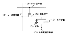
図1に、TFT駆動方式の液晶表示装置における1画素の等価回路を示す。ゲート信号線100とソース信号線101との交差部には、画素TFT102が配置され、画素TFT102のゲート端子はゲート信号線100に電気的に接続し、画素TFT102の入出力端子(ソースまたはドレイン端子)の一方はソース信号線101に接続し、もう一方には液晶103と保持容量104が接続されている。
【0004】
ゲート信号線100から画素TFT102に出力される信号に応じて画素TFT102がON状態になると、ソース信号線101の電位は、液晶103と保持容量104に書き込まれ、電荷が蓄積される。その後、画素TFT102がOFF状態になっても、液晶103と保持容量104に蓄積された電荷が、書き込まれた電位を保持しようとする。保持容量104は、スイッチング素子となる画素TFT102のoff電流、保持時間、寄生容量等によって必要な値が決まる。
【0005】
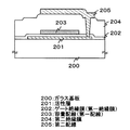
図2は、従来の保持容量の一例の断面構造を示す図である。ガラス基板200上に形成された活性層201およびゲート配線と同一膜で形成された容量配線203を電極として、その間に挟まれるように形成されたゲート絶縁膜202を誘電体として、保持容量を形成している。ゲート絶縁膜202を誘電体として用いることにより、膜厚が薄くても非常に信頼性の高い良質の保持容量を形成することができる。
【0006】
さらに、アクティブマトリクス型表示装置には遮光膜があることが望ましい。図3に、一例として画素TFTの下部に遮光膜を備えた該画素TFTの断面構造を示す。ガラス基板300上に遮光膜301、絶縁膜302を形成し、その上に画素TFTを形成するための活性層303、ゲート絶縁膜304、ゲート配線305、と重ねていく。遮光膜は光漏れを防いでコントラストを向上させ、また画素TFTを遮光することで、画素TFTのoff電流を低減する効果がある。画素TFTのoff電流が減少すると、表示データの保持特性が向上し、良好な表示が得られる。
【0007】
【発明が解決しようとする課題】
従来のアクティブマトリクス型表示装置の表示品質(画像品質)を向上させ、表示装置の省電力化、小型化、高信頼性化を達成する方法として、以下の点があげられる。
【0008】
第一に、アクティブマトリクス型表示装置において、高解像度化に伴い1画素あたりの面積が縮小しても、十分な保持容量を確保できる容量素子構造を得ることにある。各画素が大きな容量を有することが可能な保持容量を備えると、表示データの保持特性が向上し、良好な表示が得られる。
【0009】
第二に、アクティブマトリクス型表示装置において、十分な保持容量を確保しても開口率を低下させないことである。各画素が高い開口率を持つと、バックライトの光利用効率が向上し、表示装置の省電力化、小型化が達成できる。
【0010】
さらに遮光膜を配置することで、光漏れを防いでコントラストを向上させる。また、画素TFTを遮光することで、画素TFTのoff電流を低減し、表示データの保持特性の向上につながる。
【0011】
高精細化(画素TFTの微細化)、十分な保持容量の確保、大きな開口率、遮光膜、とアクティブマトリクス型表示装置の性能を向上させる要求は、一つの要求を高めると他の要求が犠牲になるという、互いに相反する要求である。これらの要求を互いに満たしながら、アクティブマトリクス型液晶表示装置の性能を向上させることが、本発明の課題である。
【0012】
【課題を解決するための手段】
前記の互いに相反する要求を満たすために、本発明人は遮光膜を使って保持容量を形成することを考えた。また、さらに大きな容量を有する保持容量を開口率をさげることなく形成する方法を提案した。
【0013】
図4(a)に、画素TFTのソース・ドレイン領域を延長して、遮光膜と容量を形成する例を断面図で示す。ガラス基板400上に、遮光膜401、誘電体(第一絶縁膜)402を形成する。画素TFTのソース・ドレイン領域のうち、画素電極409に電気的に接続されている方を、必要な保持容量が確保できるように面積を広げて活性層403を形成する。
【0014】
遮光膜401は導電性を有し、画素領域の外でCOMMON電位や電源など、一定の電位になるように接続すればよい。遮光膜401の容量が画素の保持容量に比べて十分に大きい場合など、定電位に接続しなくても、遮光膜の電位変動が十分に小さければよい。こうして活性層403と遮光膜401の間で保持容量が形成される。
【0015】
図4(b)は、遮光膜401と活性層403で形成された保持容量に加えて、さらに容量配線410を形成し、より大きな容量を有する保持容量を確保しようとした図である。活性層403の上にゲート絶縁膜404を形成し、ゲート配線405と同時に容量配線410を形成する。容量配線410は、画素領域の外でCOMMON電位や電源など、一定の電位に接続され、活性層403との間で容量を形成する。このようにして、開口率を下げることなく、さらに大きな保持容量を確保している。また図4(b)では、容量配線410の下部に形成されたゲート絶縁膜を薄く形成し、保持容量を大きくする工夫をしている。
【0016】
図4では、画素TFTのソース・ドレイン領域の両方に下部に配置した遮光膜401との容量が形成されるが、ソース信号線が接続されている方とは、容量をもたせたくない。ソース信号線に容量が形成されると、ソース信号線にビデオ信号を書き込む時の負荷が増えてしまうからである。そこで図5のように、遮光膜を2層にわけ、ソース信号線が接続されている方とは、容量を形成しないようにした構造を提案する。
【0017】
図5(a)に、遮光膜を2層使った例を示す。ガラス基板500上に第一の遮光膜501を形成し、絶縁膜502で絶縁して、第二の遮光膜503を形成する。図5では、第一の遮光膜501は画素TFTのソース・ドレイン領域のうち、ソース信号線に接続されているほうを遮光し、活性層505と容量をもたないようにしている。さらに、第一の遮光膜501は、さらにゲート配線507にコンタクトをとることで、ゲート信号線として使用している。
【0018】
第二の遮光膜503は、画素TFTのソース・ドレイン領域のうち、画素電極に接続されているほうを遮光し、活性層505と容量を形成する。第一の遮光膜501と第二の遮光膜503を合わせて、活性層505に光が入射しないように構成する。図5(b)は、図5(a)に容量配線512を設けたものである。
【0019】
なお、遮光膜で遮光されていない部分というのは、基板側から見て、見える部分のことをいう。第一の遮光膜501と第二の遮光膜503により、活性層505が有するゲート電極下のチャネル部(チャネル形成領域)、LDD領域、オフセット領域は少なくとも遮光したほうがよい。
【0020】
【発明の実施の形態】
本発明による、アクティブマトリクス型表示装置の遮光膜を容量電極(保持容量)に使った表示装置(液晶表示装置あるいはEL表示装置等)の作製プロセスについて、図面を用いて説明する。
【0021】
【実施例】
[実施例1]
ここではアクティブマトリクス基板の作製方法、特に画素部を作製する方法について、図6〜図8を用いて説明する。画素部は、画素に設けられたTFTである画素TFTのある領域(TFT形成領域)と、表示領域とからなる。なお、本明細書中において「電極」とは「配線」の一部であり、説明の便宜上、「配線」と「電極」とを使い分けるが、「電極」という言葉に「配線」は常に含められているものとする。
【0022】
図6(A)において、基板600にはガラス基板や石英基板を使用することができる。その他にもシリコン基板、金属基板またはステンレス基板の表面に絶縁膜を形成したものを基板として用いてもよい。耐熱性が許せば、プラスチック基板を用いることも可能である。そして、第一遮光膜601として、ポリシリコン膜50nmとタングステンシリサイド(W-Si)膜100nmとを島状に積層して形成する。
【0023】
第一遮光膜601上に第一絶縁膜602を形成する(図6(B))。本実施例では、第一絶縁膜602として100〜1000nm(代表的には300〜500nm)の厚さの酸化シリコン膜を用いる。なお、第一絶縁膜602としては、シリコンを含む窒化膜や酸化窒化シリコン膜を用いてもよい。さらに、第一絶縁膜602上に第二遮光膜603として、ポリシリコン膜50nmとタングステンシリサイド(W-Si)膜100nmとを島状に積層して形成する。
【0024】
なお、第一遮光膜601、第二遮光膜602としては、タングステン膜以外にも、タンタル(Ta)、チタン(Ti)、モリブデン(Mo)、タングステン(W)、クロム(Cr)、シリコン(Si)から選ばれた元素、または前記元素を組み合わせた合金膜を用いることができる。
【0025】
次に、第二絶縁膜604として、酸化シリコン膜を10〜150nmの厚さに形成する(図6(C))。なお、第二絶縁膜604は、第二遮光膜603とTFTの活性層で容量を形成する誘電体となる。第二遮光膜603としては、本実施例の遮光膜の厚さ150nmの2倍の300nm以上でつけたいところであるが、単位面積当たりの容量が少なくなってしまうので、少なくとも300nm以下、好ましくは150nm以下がよい。
【0026】
次いで、第二絶縁膜604の上に10〜100nmの厚さの、非晶質半導体膜(本実施例では非晶質シリコン膜(アモルファスシリコン膜)605)を公知の成膜法で形成する。なお、非晶質半導体膜としては、非晶質シリコン膜以外にも、非晶質シリコンゲルマニウム膜などの非晶質の化合物半導体膜を用いることもできる。
【0027】
そして、特開平7−130652号公報(USP5,643,826号に対応)に記載された技術に従って結晶構造を含む半導体膜(本実施例では結晶質シリコン膜)606を形成する。同公報記載の技術は、非晶質シリコン膜の結晶化に際して、結晶化を助長する触媒元素(ニッケル、コバルト、錫、鉛、パラジウム、鉄、銅から選ばれた一種または複数の元素、代表的にはニッケル)を用いる結晶化手段である。
【0028】
具体的には、非晶質シリコン膜表面に触媒元素を保持させた状態で加熱処理を行い、非晶質シリコン膜を結晶質シリコン膜に変化させるものである。本実施例では同公報の実施例1に記載された技術を用いるが、実施例2に記載された技術を用いてもよい。なお、結晶質シリコン膜にはいわゆる単結晶シリコン膜も多結晶シリコン膜も含まれるが、本実施例で形成される結晶質シリコン膜は結晶粒界を有するシリコン膜である。
【0029】
非晶質シリコン膜は含有水素量にもよるが、好ましくは400〜550℃で数時間加熱処理して脱水素処理を行い、含有水素量を5atomic%以下として結晶化の工程を行うことが望ましい。また、非晶質シリコン膜をスパッタ法や蒸着法などの他の作製法で形成してもよいが、膜中に含まれる酸素、窒素などの不純物元素を十分に低減させておくことが望ましい。
【0030】
又は他の結晶化の方法として、非晶質シリコン膜605に対して、レーザーから発する光(レーザー光)を照射して結晶質シリコン膜606を形成してもよい。レーザーとしては、パルス発振型または連続発振型のエキシマレーザーを用いればよいが、連続発振型のアルゴンレーザーでもよい。または、Nd:YAGレーザーもしくはNd:YVO4レーザーの第二高調波、第三高調波または第四高調波を用いてもよい。さらに、レーザー光のビーム形状は線状(長方形状も含む)であっても矩形状であってもかまわない。
【0031】
また、レーザー光のかわりにランプから発する光(ランプ光)を照射(以下、ランプアニールという)してもよい。ランプ光としては、ハロゲンランプ、赤外線ランプ等から発するランプ光を用いることができる。
【0032】
このようにレーザー光またはランプ光により熱処理(アニール)を施す工程を光アニール工程という。光アニール工程は短時間で高温熱処理が行えるため、ガラス基板等の耐熱性の低い基板を用いる場合にも効果的な熱処理工程を高いスループットで行うことができる。もちろん、目的はアニールであるので電熱炉を用いたファーネスアニール(熱アニールともいう)で代用することもできる。
【0033】
本実施例では、パルス発振型エキシマレーザー光を線状に加工してレーザーアニール工程を行った。レーザーアニール条件は、励起ガスとしてXeClガスを用い、処理温度を室温、パルス発振周波数を30Hzとし、レーザーエネルギー密度を250〜500mJ/cm2(代表的には350〜400mJ/cm2)とする。
【0034】
上記条件で行われるレーザーアニール工程は、熱結晶化後に残存した非晶質領域を完全に結晶化するとともに、既に結晶化された結晶質領域の欠陥等を低減する効果を有する。そのため、本工程は光アニールにより半導体膜の結晶性を改善する工程、または半導体膜の結晶化を助長する工程と呼ぶこともできる。このような効果はランプアニールの条件を最適化することによっても得ることが可能である。
【0035】
次に、結晶質シリコン膜606上に、後の不純物添加工程のために保護膜607を形成する。保護膜607は100〜200nm(好ましくは130〜170nm)の厚さの窒化酸化シリコン膜または酸化シリコン膜を用いる。この保護膜607は不純物添加工程の際に結晶質シリコン膜606が直接プラズマにさらされないようにするためと、微妙な温度制御を可能にするために用いられる。
【0036】
続いて、保護膜607を介してp型を付与する不純物元素(以下、p型不純物元素という)を添加する。p型不純物元素としては、代表的には周期表の13族に属する元素、典型的にはボロンまたはガリウムを用いることができる。この工程(チャネルドープ工程という)は、TFTしきい値電圧を制御するための工程である。なお、ここではジボラン(B2H6)を質量分離しないでプラズマ励起したイオンドープ法でボロンを添加した。もちろん、質量分離を行うイオンインプランテーション法を用いてもよい。
【0037】
この工程により1×10¹⁵〜1×10¹⁸atoms/cm3(代表的には5×1016〜5×1017atoms/cm3)の濃度で、p型不純物元素(本実施例ではボロン)を含むp型不純物領域(a)608を形成する(図6(E))。
【0038】
次に、保護膜607を除去した後、結晶質シリコン膜の不要な部分を除去して、島状の半導体膜(以下、活性層という)609を形成する(図6(F))。
【0039】
次いで、活性層609を覆って、ゲート絶縁膜610を形成する(図6(G))。ゲート絶縁膜610は、10〜200nm、好ましくは50〜150nmの厚さに形成すればよい。本実施例では、プラズマCVD法でN2OとSiH4を原料とした窒化酸化シリコン膜を二回成膜する。まず、第一窒化酸化シリコン膜(絶縁膜)を20nm成膜する。次いで、容量配線を形成する領域の第一窒化酸化シリコン膜(絶縁膜)をエッチングする。そして、第二窒化酸化シリコン膜(絶縁膜)を60nm成膜する。そうすると、容量配線の下は60nmの絶縁膜(第二窒化酸化シリコン膜)、TFTのチャネル部には80nmのゲート絶縁膜(第一窒化酸化シリコン膜+第二酸化窒化シリコン膜)ができる。つまり、活性層と容量配線で挟まれた絶縁膜の厚さは60nmであり、活性層とゲート電極で挟まれた絶縁膜の厚さは80nmとなっており、厚さが異なっている。
【0040】
厚さ20nmで絶縁膜(ゲート絶縁膜)を形成した部分だけを残してレジストマスク611で覆い、n型不純物元素(本実施例ではリン)を添加して高濃度にリンを含むn型不純物領域(a)612を形成する(図7(A))。n型不純物領域(a)612は、フォスフィン(PH3)を用いたイオンドープ法(もちろん、イオンインプランテーション法でもよい)で行い、この領域のリンの濃度は1×10²⁰〜1×10²¹atoms/cm3(代表的には2×1020〜5×1020atoms/cm3)とする。また、n型不純物領域(a)612が形成された領域には、すでに前工程で添加されたボロンが含まれるが、十分に高い濃度でリンが添加されることになるので、前工程で添加されたボロンの影響は考えなくてよい。
【0041】
レジストマスク611を除去し、第一遮光膜からゲート配線にコンタクトをとるための開孔部613を形成する(図7(B))。本実施例では、第一遮光膜がゲート信号線の役割をはたすので、画素部で第一遮光膜とゲート配線をつなぐコンタクトを形成する。
【0042】
図示しないが、ゲート配線614として、厚さ50nmの窒化タングステン(WN)と、厚さ350nmのタンタル(Ta)との2層の積層膜を形成する(図7(C))。ゲート配線614は単層の導電膜で形成してもよいが、必要に応じて2層、3層といった積層膜とすることが好ましい。
【0043】
なお、ゲート配線614としては、タンタル(Ta)、チタン(Ti)、モリブデン(Mo)、タングステン(W)、クロム(Cr)、シリコン(Si)から選ばれた元素、または前記元素を組み合わせた合金膜(代表的には、Mo-W合金、Mo-Ta合金)を用いることができる。
【0044】
次に、ゲート配線614をマスクとして自己整合的にn型不純物元素(本実施例ではリン)を添加する(図7(D))。こうして形成されたn型不純物領域(b)615には、前記のチャネルドープ工程で添加されたボロン濃度よりも5〜10倍高い濃度(代表的には1×10¹⁶〜5×10¹⁸atoms/cm3、典型的には3×1017〜3×1018atoms/cm3)でリンが添加されるように調整する。
【0045】
レジストマスク616を形成し、n型不純物元素(本実施例ではリン)を添加して、高濃度にリンを含むn型不純物領域(C)617を形成する(図7(E))。この工程においても、フォスフィン(PH3)を用いたイオンドープ法(もちろん、イオンインプランテーション法でもよい)で行い、この領域のリンの濃度は1×10²⁰〜1×10²¹atoms/cm3(代表的には2×1020〜5×1020atoms/cm3)とする。
【0046】
また、n型不純物領域(C)617が形成された領域には、すでに前工程で添加されたリンまたはボロンが含まれるが、十分に高い濃度でリンが添加されることになるので、前工程で添加されたリンまたはボロンの影響は考えなくてよい。
【0047】
レジストマスク616を除去した後、第四絶縁膜618を形成する(図8(A))。第四絶縁膜618としては、シリコンを含む絶縁膜、具体的には窒化シリコン膜、酸化シリコン膜、窒化酸化シリコン膜またはそれらを組み合わせた積層膜で形成し、膜厚は600nm〜1.5μmとすればよい。本実施例では、第四絶縁膜618としてプラズマCVD法でSiH4、N2O、NH3を原料ガスとし、1μm厚の窒化酸化シリコン膜(但し窒素濃度が25〜50atomic%)を用いる。
【0048】
その後、それぞれの濃度で添加されたn型またはp型不純物元素を活性化するために熱処理工程を行う(図8(A))。この工程はファーネスアニール法、レーザーアニール法、またはラピッドサーマルアニール(RTA)法で行うことができる。ここでは、ファーネスアニール法で活性化工程を行う。加熱処理は窒素雰囲気中において300〜650℃、好ましくは400〜550℃で行う。本実施例では、550℃、4時間の熱処理を行う。
【0049】
このように、触媒元素を用いて結晶化を行った場合、非晶質シリコン膜の結晶化に用いた触媒元素(本実施例ではニッケル)が、矢印で示す方向に移動して、前記の図7(E)の工程で形成された高濃度にリンを含むn型不純物領域(C)617に捕獲(ゲッタリング)される。これは、リンによる金属元素のゲッタリング効果に起因する現象であり、この結果、チャネル領域619は前記触媒元素の濃度が1×10¹⁷atoms/cm3以下(好ましくは1×1016atoms/cm3以下)となる。
【0050】
また、触媒元素のゲッタリングサイトとなった領域(図7(E)の工程で形成されたn型不純物領域(C)617)は高濃度に触媒元素が偏析して、5×10¹⁸atoms/cm3以上(代表的には1×1019〜5×1020atoms/cm3)の濃度となる。
【0051】
さらに、3〜100%の水素を含む雰囲気中で、300〜450℃で1〜12時間の熱処理を行い、活性層を水素化する工程を行う。この工程は熱的に励起された水素により、半導体層のダングリングボンドを終端する工程である。水素化の他の手段として、プラズマ水素化(プラズマにより励起された水素を用いる)を行ってもよい。
【0052】
その後、TFTのソース・ドレイン領域に達する開孔部620(図8(B))、ソース・ドレイン配線621を形成する(図8(C))。また、図示していないが、本実施例ではこの配線を、Ti膜を100nm、Tiを含むアルミニウム膜を300nm、Ti膜150nmをスパッタ法で連続して形成した3層構造の積層膜で形成した。
【0053】
次に、パッシベーション膜622として、窒化シリコン膜、酸化シリコン膜、または窒化酸化シリコン膜で50〜500nm(代表的には200〜300nm)の厚さで形成する(図8(D))。この時、本実施例では膜の形成に先立ってH2、NH3等水素を含むガスを用いてプラズマ処理を行い、成膜後に熱処理を行う。この前処理により励起された水素が第四絶縁膜618中に供給される。この状態で熱処理を行うことで、パッシベーション膜622の膜質を改善するとともに、第四絶縁膜618中に添加された水素が下方側に拡散するため、効果的に活性層を水素化することができる。
【0054】
また、パッシベーション膜622を形成した後に、さらに水素化工程を行ってもよい。例えば、3〜100%の水素を含む雰囲気中で、300〜450℃で1〜12時間の熱処理を行うとよい。あるいはプラズマ水素化法を用いても同様の効果が得られる。なお、この工程において、後に画素電極とソース・ドレイン配線を接続するための開孔部を形成する位置において、パッシベーション膜622に開孔部を形成しておいてもよい。
【0055】
その後、有機樹脂からなる第五絶縁膜623を約1μmの厚さに形成する(図8(D))。有機樹脂としては、ポリイミド、アクリル、ポリアミド、ポリイミドアミド、BCB(ベンゾシクロブテン)等を使用することができる。有機樹脂膜を用いることの利点は、成膜方法が簡単である点や、比誘電率が低いので、寄生容量を低減できる点、平坦性に優れる点などが上げられる。なお、本発明は、上述した以外の有機樹脂膜や有機系SiO化合物などあらゆる材料を用いることができる。本実施例では、基板に塗布後、熱重合するタイプのポリイミドを用い、300℃で焼成して形成する。
【0056】
次に、第五絶縁膜623及びパッシベーション膜622にソース・ドレイン配線621に達する開孔部624を形成し、画素電極625を形成する(図8(D、E))。画素電極625は、透過型液晶表示装置とする場合には透明導電膜を用い、反射型の液晶表示装置とする場合には金属膜を用いれば良い。ここでは透過型の液晶表示装置とするために、酸化インジウム・スズ(ITO)膜を110nmの厚さにスパッタ法で形成する。
【0057】
こうして画素部には、表示領域627の面積を確保しつつ、nチャネル型TFTでなる画素TFT領域626が形成され、十分な保持容量を得ることができる。
【0058】
なお、本実施例では形成しなかったが、結晶質シリコン膜606に、公知の方法を用いてLDD領域を形成してもよい。なお、本明細書において、LDD領域とは、低濃度不純物領域(Light-Doped-Drain領域)を指す。また、結晶質シリコン膜606には公知の方法を用いて、オフセット領域を形成してもよい。なお、本明細書において、オフセット領域とは、ゲート電極からずらして不純物元素を打ち込んだ領域のことを指す。
【0059】
[実施例2]
本実施例では、実施例1で作製したアクティブマトリクス基板から、アクティブマトリクス型液晶表示装置を作製する工程を説明する。図9に示すように、図8(E)の状態の基板に対し、配向膜901を形成する。本実施例では配向膜としてポリイミド膜を用いた。また、対向基板905には、透明導電膜で対向電極904を、そして配向膜903を形成する。なお、対向基板には必要に応じてカラーフィルターや遮蔽膜を形成しても良い。
【0060】
配向膜を形成した後、ラビング処理を施して液晶分子がある一定のプレチルト角を持って配向するようにする。そして、画素部と駆動回路が形成されたアクティブマトリクス基板と対向基板とを、公知のセル組み工程によってシール材やスペーサ(共に図示せず)などを介して貼りあわせる。その後、両基板の間に液晶902を注入し、封止剤(図示せず)によって完全に封止する。液晶には公知の液晶材料を用いれば良い。このようにして図9に示すアクティブマトリクス型液晶表示装置が完成する。
【0061】
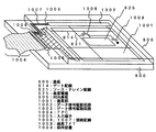
次に、このアクティブマトリクス型液晶表示装置の構成を、図10の斜視図を用いて説明する。尚、図10は、図6〜図9の断面構造図と対応付けるため、共通の符号を用いている。アクティブマトリクス基板は、ガラス基板600上に形成された画素部1001と、ゲート信号駆動回路1003と、データ(ソース)信号駆動回路1002で構成される。画素TFT1008はnチャネル型TFTであり、周辺に設けられる駆動回路はCMOS回路を基本として構成されている。ゲート信号駆動回路1003と、データ信号駆動回路1002はそれぞれゲート配線614とソース・ドレイン配線621(ソース信号線)で画素部1001に接続されている。また、FPC1004が接続された入力端子1005から駆動回路の入出力端子までの接続配線1006、1007が設けられている。
【0062】
なお、本実施例は、実施例1と自由に組み合わせることが可能である。
【0063】
[実施例3]
本実施例では、本発明を用いてEL(エレクトロルミネセンス)表示装置を作製した例について説明する。なお、図11は本発明のEL表示装置の上面図であり、図12はその断面図である。
【0064】
図11、12において、4001は基板、4002は画素部、4003はソース信号駆動回路、4004はゲート信号駆動回路であり、それぞれの駆動回路は接続配線4005を経てFPC(フレキシブルプリントサーキット)4006に至り、外部機器へと接続される。
【0065】
このとき、画素部4002、ソース信号駆動回路4003及びゲート信号駆動回路4004を囲むようにして第1シール材4101、カバー材4102、充填材4103及び第2シール材4104が設けられている。
【0066】
図12は、図11をA―A'で切断した断面図に相当し、基板4001の上にソース信号駆動回路4003に含まれる駆動TFT(但し、ここではnチャネル型TFTとpチャネル型TFTを図示している)4201及び画素部4002に含まれる画素TFT(但し、ここではEL素子への電流を制御するTFTを図示している)4202が形成されている。
【0067】
本実施例では、本発明の容量素子構造を用いて画素TFT4202が作製される。すなわち、画素TFT4202には図8(E)と同じ構造のTFTが用いられる。
【0068】
駆動TFT4201及び画素TFT4202の上には樹脂材料でなる層間絶縁膜(平坦化膜)4301が形成され、その上に画素TFT4202のソース・ドレイン領域の一方と電気的に接続する画素電極4302が形成される。画素電極4302としては仕事関数の大きい透明導電膜が用いられる。透明導電膜としては、酸化インジウムと酸化スズとの化合物または酸化インジウムと酸化亜鉛との化合物を用いることができる。
【0069】
そして、画素電極4302の上には絶縁膜4303が形成され、絶縁膜4303は画素電極4302の上に開口部が形成されている。この開口部において、画素電極4302の上にはEL層4304が形成される。EL層4304は公知の有機EL材料または無機EL材料を用いることができる。また、有機EL材料には低分子系(モノマー系)材料と高分子系(ポリマー系)材料があるがどちらを用いても良い。
【0070】
EL層4304の形成方法は公知の技術を用いれば良い。また、EL層の構造は正孔注入層、正孔輸送層、発光層、電子輸送層または電子注入層を自由に組み合わせて積層構造または単層構造とすれば良い。
【0071】
EL層4304の上には遮光性を有する導電膜(代表的にはアルミニウム、銅もしくは銀を主成分とする導電膜またはそれらと他の導電膜との積層膜)からなる陰極4305が形成される。また、陰極4305とEL層4304の界面に存在する水分や酸素は極力排除しておくことが望ましい。従って、真空中で両者を連続成膜するか、EL層4304を窒素または希ガス雰囲気で形成し、酸素や水分に触れさせないまま陰極4305を形成するといった工夫が必要である。本実施例ではマルチチャンバー方式(クラスターツール方式)の成膜装置を用いることで上述のような成膜を可能とする。
【0072】
そして陰極4305は4306で示される領域において接続配線4005に電気的に接続される。接続配線4005は陰極4305に所定の電圧を与えるための配線であり、導電性材料4307を介してFPC4006に電気的に接続される。
【0073】
以上のようにして、画素電極4302、EL層4304及び陰極4305からなるEL素子が形成される。このEL素子は、第1シール材4101によって基板4001に貼り合わされたカバー材4102で囲まれ、充填材4103により封入されている。
【0074】
なお、本明細書において、EL素子(発光素子)は一対の電極(陽極と陰極)間にEL層(有機化合物層)が挟まれた構造とする。有機化合物層は、公知の発光材料を用いて作製することが出来る。また、有機化合物層には、単層構造と積層構造の二つの構造があるが、本発明はどちらの構造を用いてもよい。なお、有機化合物層におけるルミネッセンスには、一重項励起状態から基底状態に戻る際の発光(蛍光)と、三重項励起状態から基底状態に戻る際の発光(リン光)とがあるが、本発明はどちらの発光を用いた発光装置にも適用することが出来る。
【0075】
カバー材4102としては、ガラス板、金属板(代表的にはステンレス板)、セラミックス板、FRP(Fiberglass Reinforced Plastics)板、PVF(ポリビニルフルオライド)フィルム、マイラーフィルム、ポリエステルフィルムまたはアクリルフィルムを用いることができる。また、アルミニウムホイルをPVFフィルムやマイラーフィルムで挟んだ構造のシートを用いることもできる。
【0076】
但し、EL素子からの光の放射方向がカバー材側に向かう場合にはカバー材は透明でなければならない。その場合には、ガラス板、プラスチック板、ポリエステルフィルムまたはアクリルフィルムのような透明物質を用いる。
【0077】
また、充填材4103としては紫外線硬化樹脂または熱硬化樹脂を用いることができ、PVC(ポリビニルクロライド)、アクリル、ポリイミド、エポキシ樹脂、シリコーン樹脂、PVB(ポリビニルブチラル)またはEVA(エチレンビニルアセテート)を用いることができる。この充填材4103の内部に吸湿性物質(好ましくは酸化バリウム)を設けておくとEL素子の劣化を抑制できる。
【0078】
また、充填材4103の中にスペーサを含有させてもよい。このとき、スペーサを酸化バリウムで形成すればスペーサ自体に吸湿性をもたせることが可能である。また、スペーサを設けた場合、スペーサからの圧力を緩和するバッファ層として陰極4305上に樹脂膜を設けることも有効である。
【0079】
また、接続配線4005は導電性材料4307を介してFPC4006に電気的に接続される。接続配線4005は画素部4002、ソース信号駆動回路4003及びゲート信号駆動回路4004に送られる信号をFPC4006に伝え、FPC4006により外部機器と電気的に接続される。
【0080】
また、本実施例では第1シール材4101の露呈部及びFPC4006の一部を覆うように第2シール材4104を設け、EL素子を徹底的に外気から遮断する構造となっている。こうして図12の断面構造を有するEL表示装置となる。なお、本実施例のEL表示装置は実施例1の構成と組み合わせて作製しても構わない。
【0081】
なお、本実施例は、実施例1乃至実施例2と自由に組み合わせることが可能である。
【0082】
[実施例4]
本実施例では、トランジスタの下部に設けた下部遮光膜に加えて、上部遮光膜を設けた表示装置の断面構造について、図14を用いて説明する。
【0083】
図14において、1910は絶縁表面を有する基板である。基板1910には、ガラス基板や石英基板等を用いることが出来る。基板1910上には遮光膜1906が設けられる。なお、遮光膜1906は、タンタル(Ta)、チタン(Ti)、モリブデン(Mo)、タングステン(W)、クロム(Cr)、シリコン(Si)から選ばれた元素、または前記元素を組み合わせた合金膜を公知の方法で形成する。また遮光膜1906は、トランジスタを遮光する機能を有する。
【0084】
次いで、遮光膜1906上に、第一絶縁膜1911が設けられ、該第一絶縁膜1911上に、半導体膜1907が設けられる。なお、本実施例では、第一絶縁膜1911として酸化シリコン膜を300nmの厚さに形成した。また、半導体膜1907は、公知の材料を用いて公知の方法で形成した。
【0085】
次いで、半導体膜1907上にゲート絶縁膜1912が設けられる。そして、ゲート絶縁膜1912上には、ゲート電極1908と容量配線1909が設けられる。なお、本実施例において、遮光膜1906と、半導体膜1907と、容量配線1909との重なっている領域が保持容量に相当する。
【0086】
1913は第二絶縁膜である。本実施例では、第二絶縁膜1913として酸化シリコン膜を形成した。そして、ゲート絶縁膜1912及び第二絶縁膜1913にはコンタクトホールが形成され、ソース配線1917及びドレイン配線1918が設けられる。
【0087】
1914は第三絶縁膜である。本実施例では、第三絶縁膜1913として酸化シリコン膜を形成した。第三絶縁膜1913上には、公知の材料を用いて形成された上部遮光膜1916が設けられている。上部遮光膜1916は、公知の材料を用いて形成され、トランジスタを遮光する機能を有する。
【0088】
1920は第四絶縁膜である。次いで、第三絶縁膜1914及び第四絶縁膜1920にコンタクトホールが形成され、画素電極1919が設けられる。
【0089】
図14に示すように、画素電極1919は、ドレイン配線1918と電気的に接続されている。なお、本実施例においては、画素電極1919は、ドレイン配線1918と接続されているが、本発明はこれに限定されず、ソース配線1917と接続されていてもよい。なお、画素電極に接続されたソース領域及びドレイン領域の一方は、他方よりも広い面積を有する。
【0090】
1901は配向膜である。本実施例では配向膜1901としてポリイミド膜を用いた。また、対向基板1905には、透明導電膜で対向電極1904と、配向膜1903を形成する。なお、対向基板1905には必要に応じてカラーフィルターや遮蔽膜を形成しても良い。
【0091】
配向膜1903を形成した後には、ラビング処理を施して液晶分子がある一定のプレチルト角を持って配向するようにする。そして、画素部と駆動回路が形成されたアクティブマトリクス基板と対向基板とを、公知のセル組み工程によってシール材やスペーサ(共に図示せず)などを介して貼りあわせる。その後、両基板の間に液晶1902を注入し、封止剤(図示せず)によって完全に封止する。液晶1902は公知の液晶材料を用いれば良い。このようにして図14に示すアクティブマトリクス型液晶表示装置が完成する。
【0092】
なお、本実施例は、実施例1乃至実施例3と自由に組み合わせることが可能である。
【0093】
[実施例5]
本発明のアクティブマトリクス型表示装置は電気器具の表示部として用いることができる。そのような電気器具としては、ビデオカメラ、デジタルカメラ、プロジェクター、プロジェクションTV、ゴーグル型ディスプレイ(ヘッドマウントディスプレイ)、ナビゲーションシステム、音響再生装置、ノート型パーソナルコンピュータ、ゲーム機器、携帯情報端末(モバイルコンピュータ、携帯電話、携帯型ゲーム機または電子書籍等)、記録媒体を備えた画像再生装置などが挙げられる。それら電気器具の具体例を図13に示す。
【0094】
図13(A)は携帯電話であり、本体2001、音声出力部2002、音声入力部2003、表示部2004、操作スイッチ2005、アンテナ2006で構成される。本発明のアクティブマトリクス型表示装置は表示部2004に用いることができる。
【0095】
図13(B)はビデオカメラであり、本体2101、表示部2102、音声入力部2103、操作スイッチ2104、バッテリー2105、受像部2106で構成される。本発明のアクティブマトリクス型表示装置は表示部2102に用いることができる。
【0096】
図13(C)はモバイルコンピュータ(モービルコンピュータ)であり、本体2201、カメラ部2202、受像部2203、操作スイッチ2204、表示部2205で構成される。本発明のアクティブマトリクス型表示装置は表示部2205に用いることができる。
【0097】
図13(D)はゴーグル型ディスプレイであり、本体2301、表示部2302、アーム部2303で構成される。本発明のアクティブマトリクス型表示装置は表示部2302に用いることができる。
【0098】
図13(E)はリアプロジェクター(プロジェクションTV)であり、本体2401、光源2402、液晶表示装置2403、偏光ビームスプリッタ2404、リフレクター2405、2406、スクリーン2407で構成される。本発明は液晶表示装置2403に用いることができる。
【0099】
図13(F)はフロントプロジェクターであり、本体2501、光源2502、液晶表示装置2503、光学系2504、スクリーン2505で構成される。
本発明は液晶表示装置2503に用いることができる。
【0100】
以上の様に、本発明の適用範囲は極めて広く、あらゆる分野の電気器具に適用することが可能である。また、本実施例の電気器具は実施例1〜4のどのような組み合わせからなる構成を用いても実現することができる。
【0101】
【発明の効果】
本発明を用いた保持容量を有するアクティブマトリクス型表示装置を作製すれば、1画素の面積が縮小しても、遮光膜を用いて十分な保持容量が確保できるため、表示品位を向上できる。同時に、本発明を用いたアクティブマトリクス型表示装置を表示部として用いた電気器具の品質をも向上させることができる。
【0102】
【図面の簡単な説明】
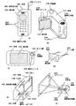
【図1】 アクティブマトリクス型液晶表示装置の1画素の等価回路を示す図。
【図2】 従来の保持容量構造を示す断面図。
【図3】 画素TFTの下部に遮光膜を備えた図
【図4】 本発明における保持容量の構造を示す図。
【図5】 本発明における保持容量の構造を示す図。
【図6】 実施例1の画素部の作製工程を示す図。
【図7】 実施例1の画素部の作製工程を示す図。
【図8】 実施例1の画素部の作製工程を示す図。
【図9】 アクティブマトリクス型液晶表示装置の断面図。
【図10】 アクティブマトリクス型液晶表示装置の斜視図。
【図11】 アクティブマトリクス型EL表示装置の構成を示す図。
【図12】 アクティブマトリクス型EL表示装置の構成を示す断面図。
【図13】 電気器具の一例を示す図。
【図14】 アクティブマトリクス型表示装置の断面図。[0001]
BACKGROUND OF THE INVENTION
The present invention relates to an active matrix display device using a thin film transistor (hereinafter referred to as TFT) as a switching element. More specifically, the present invention relates to a pixel structure of the active matrix display device.
[0002]
[Prior art]
As an active matrix type display device, a liquid crystal display device of a method of driving using TFTs (TFT driving method) is known. Since the liquid crystal display device can control the voltage applied to the liquid crystal for each pixel by a TFT formed on a transparent substrate such as glass, the image is clear and is widely used in OA devices, TVs, and the like. .
[0003]
FIG. 1 shows an equivalent circuit of one pixel in a TFT drive type liquid crystal display device. A pixel TFT 102 is disposed at an intersection between the
[0004]
When the pixel TFT 102 is turned on in response to a signal output from the
[0005]
FIG. 2 is a diagram showing a cross-sectional structure of an example of a conventional storage capacitor. An
[0006]
Further, the active matrix display device desirably has a light shielding film. FIG. 3 shows, as an example, a cross-sectional structure of the pixel TFT provided with a light shielding film below the pixel TFT. A
[0007]
[Problems to be solved by the invention]
The following points can be mentioned as methods for improving the display quality (image quality) of a conventional active matrix display device and achieving power saving, downsizing, and high reliability of the display device.
[0008]
First, in an active matrix display device, a capacitive element structure capable of securing a sufficient storage capacity even when the area per pixel is reduced as the resolution is increased is obtained. When each pixel has a storage capacitor capable of having a large capacity, display data retention characteristics are improved, and a good display can be obtained.
[0009]
Second, in the active matrix display device, the aperture ratio is not lowered even if a sufficient storage capacity is secured. When each pixel has a high aperture ratio, the light utilization efficiency of the backlight is improved, and power saving and downsizing of the display device can be achieved.
[0010]
Furthermore, by arranging a light shielding film, light leakage is prevented and contrast is improved. Further, by shielding the pixel TFT, the off current of the pixel TFT is reduced, which leads to improvement of display data retention characteristics.
[0011]
The demand to improve the performance of high-definition (miniaturization of pixel TFT), sufficient storage capacity, large aperture ratio, light-shielding film, and active matrix display device is sacrificed if one requirement is increased. It is a mutually conflicting request to become. It is an object of the present invention to improve the performance of an active matrix liquid crystal display device while satisfying these requirements.
[0012]
[Means for Solving the Problems]
In order to satisfy the mutually conflicting requirements, the present inventor considered forming a storage capacitor using a light shielding film. In addition, a method for forming a storage capacitor having a larger capacity without reducing the aperture ratio has been proposed.
[0013]
FIG. 4A is a sectional view showing an example in which the source / drain regions of the pixel TFT are extended to form a light shielding film and a capacitor. A
[0014]
The light-
[0015]
FIG. 4B is a diagram in which in addition to the storage capacitor formed by the
[0016]
In FIG. 4, a capacitance with the
[0017]
FIG. 5A shows an example using two light shielding films. A first light-shielding
[0018]
The second
[0019]
Note that the portion that is not shielded by the light shielding film refers to a portion that can be seen from the substrate side. The first light-shielding
[0020]
DETAILED DESCRIPTION OF THE INVENTION
A manufacturing process of a display device (a liquid crystal display device, an EL display device, or the like) using a light-shielding film of an active matrix display device as a capacitor electrode (retention capacitor) according to the present invention will be described with reference to the drawings.
[0021]
【Example】
[Example 1]
Here, a method for manufacturing an active matrix substrate, in particular, a method for manufacturing a pixel portion will be described with reference to FIGS. The pixel portion includes a region (TFT formation region) where a pixel TFT, which is a TFT provided in the pixel, and a display region. In this specification, “electrode” is a part of “wiring”, and for convenience of explanation, “wiring” and “electrode” are used separately, but “wiring” is always included in the word “electrode”. It shall be.
[0022]
In FIG. 6A, a glass substrate or a quartz substrate can be used for the
[0023]
A first insulating film 602 is formed over the first light-shielding film 601 (FIG. 6B). In this embodiment, a silicon oxide film having a thickness of 100 to 1000 nm (typically 300 to 500 nm) is used as the first insulating film 602. Note that as the first insulating film 602, a nitride film containing silicon or a silicon oxynitride film may be used. Further, a polysilicon film 50 nm and a tungsten silicide (W—Si)
[0024]
As the first light shielding film 601 and the second light shielding film 602, besides the tungsten film, tantalum (Ta), titanium (Ti), molybdenum (Mo), tungsten (W), chromium (Cr), silicon (Si) Or an alloy film in which the elements are combined can be used.
[0025]
Next, a silicon oxide film is formed to a thickness of 10 to 150 nm as the second insulating film 604 (FIG. 6C). The second insulating film 604 is a dielectric that forms a capacitor with the second light shielding film 603 and the active layer of the TFT. The second light-shielding film 603 is desired to be attached at 300 nm or more, which is twice the thickness of 150 nm of the light-shielding film of this embodiment. However, since the capacity per unit area is reduced, it is at least 300 nm or less, preferably 150 nm. The following is good.
[0026]
Next, an amorphous semiconductor film (in this embodiment, an amorphous silicon film (amorphous silicon film) 605) having a thickness of 10 to 100 nm is formed on the second insulating film 604 by a known deposition method. Note that as the amorphous semiconductor film, an amorphous compound semiconductor film such as an amorphous silicon germanium film can be used in addition to the amorphous silicon film.
[0027]
Then, a semiconductor film (crystalline silicon film in this embodiment) 606 including a crystal structure is formed according to the technique described in Japanese Patent Application Laid-Open No. 7-130652 (corresponding to USP 5,643,826). The technology described in the publication is a catalyst element (one or a plurality of elements selected from nickel, cobalt, tin, lead, palladium, iron, and copper, typical for promoting crystallization in crystallization of an amorphous silicon film, Is a crystallization means using nickel).
[0028]
Specifically, heat treatment is performed with the catalytic element held on the surface of the amorphous silicon film to change the amorphous silicon film into a crystalline silicon film. In this embodiment, the technique described in the first embodiment of the publication is used, but the technique described in the second embodiment may be used. Note that the crystalline silicon film includes a so-called single crystal silicon film and a polycrystalline silicon film, but the crystalline silicon film formed in this embodiment is a silicon film having a crystal grain boundary.
[0029]
Although it depends on the amount of hydrogen contained in the amorphous silicon film, it is preferable to perform a dehydrogenation treatment by heat treatment at 400 to 550 ° C. for several hours, and to perform a crystallization step with a hydrogen content of 5 atomic% or less. . In addition, the amorphous silicon film may be formed by other manufacturing methods such as a sputtering method or an evaporation method, but it is desirable to sufficiently reduce impurity elements such as oxygen and nitrogen contained in the film.
[0030]
Alternatively, as another crystallization method, the amorphous silicon film 605 may be irradiated with light (laser light) emitted from a laser to form the crystalline silicon film 606. As the laser, a pulse oscillation type or continuous oscillation type excimer laser may be used, but a continuous oscillation type argon laser may be used. Or Nd: YAG laser or Nd: YVO Four Laser second harmonic, third harmonic, or fourth harmonic may be used. Furthermore, the beam shape of the laser light may be linear (including rectangular) or rectangular.
[0031]
Further, instead of laser light, light emitted from a lamp (lamp light) may be irradiated (hereinafter referred to as lamp annealing). As the lamp light, lamp light emitted from a halogen lamp, an infrared lamp or the like can be used.
[0032]
The process of performing heat treatment (annealing) with laser light or lamp light in this way is called a light annealing process. Since the light annealing process can be performed at a high temperature in a short time, an effective heat treatment process can be performed with high throughput even when a substrate having low heat resistance such as a glass substrate is used. Of course, since the purpose is annealing, furnace annealing (also referred to as thermal annealing) using an electric furnace can be used instead.
[0033]
In this example, a pulsed excimer laser beam was processed into a linear shape and a laser annealing process was performed. The laser annealing conditions are as follows: XeCl gas is used as the excitation gas, the processing temperature is room temperature, the pulse oscillation frequency is 30 Hz, and the laser energy density is 250 to 500 mJ / cm. 2 (Typically 350-400mJ / cm 2 ).
[0034]
The laser annealing step performed under the above conditions has an effect of completely crystallizing the amorphous region remaining after the thermal crystallization and reducing defects or the like of the already crystallized crystalline region. Therefore, this step can also be called a step of improving the crystallinity of the semiconductor film by light annealing or a step of promoting the crystallization of the semiconductor film. Such an effect can also be obtained by optimizing the lamp annealing conditions.
[0035]
Next, a protective film 607 is formed on the crystalline silicon film 606 for a subsequent impurity addition step. As the protective film 607, a silicon nitride oxide film or a silicon oxide film with a thickness of 100 to 200 nm (preferably 130 to 170 nm) is used. The protective film 607 is used to prevent the crystalline silicon film 606 from being directly exposed to plasma during the impurity addition step and to enable delicate temperature control.
[0036]
Subsequently, an impurity element imparting p-type conductivity (hereinafter referred to as a p-type impurity element) is added through the protective film 607. As the p-type impurity element, an element belonging to Group 13 of the periodic table, typically boron or gallium can be typically used. This step (referred to as channel doping step) is a step for controlling the TFT threshold voltage. Here, diborane (B 2 H 6 Boron was added by ion doping with plasma excitation without mass separation. Of course, an ion implantation method that performs mass separation may be used.
[0037]
1x10 by this process 15 ~ 1x10 18 atoms / cm Three (Typically 5 × 10 16 ~ 5x10 17 atoms / cm Three ), A p-type impurity region (a) 608 containing a p-type impurity element (boron in this embodiment) is formed (FIG. 6E).
[0038]
Next, after removing the protective film 607, an unnecessary portion of the crystalline silicon film is removed to form an island-shaped semiconductor film (hereinafter referred to as an active layer) 609 (FIG. 6F).
[0039]
Next, a gate insulating film 610 is formed so as to cover the active layer 609 (FIG. 6G). The gate insulating film 610 may be formed to a thickness of 10 to 200 nm, preferably 50 to 150 nm. In this embodiment, plasma CVD is used for N. 2 O and SiH Four A silicon nitride oxide film is formed twice using as a raw material. First, a first silicon nitride oxide film (insulating film) is formed to a thickness of 20 nm. Next, the first silicon nitride oxide film (insulating film) in the region where the capacitor wiring is formed is etched. Then, a second silicon nitride oxide film (insulating film) is formed to a thickness of 60 nm. Then, an insulating film (second silicon nitride oxide film) having a thickness of 60 nm is formed under the capacitor wiring, and a gate insulating film (first silicon nitride oxide film + first silicon dioxide nitride film) having a thickness of 80 nm is formed in the channel portion of the TFT. That is, the thickness of the insulating film sandwiched between the active layer and the capacitor wiring is 60 nm, and the thickness of the insulating film sandwiched between the active layer and the gate electrode is 80 nm, which are different in thickness.
[0040]
An n-type impurity region containing phosphorus at a high concentration by adding an n-type impurity element (phosphorus in this embodiment) by covering only with a resist mask 611 while leaving only a portion where an insulating film (gate insulating film) is formed with a thickness of 20 nm. (A) 612 is formed (FIG. 7A). The n-type impurity region (a) 612 includes phosphine (PH Three ) Using an ion doping method (of course, an ion implantation method may be used), and the phosphorus concentration in this region is 1 × 10 20 ~ 1x10 twenty one atoms / cm Three (Typically 2 × 10 20 ~ 5x10 20 atoms / cm Three ). In addition, the region where the n-type impurity region (a) 612 is formed contains boron already added in the previous step, but phosphorus is added at a sufficiently high concentration. There is no need to consider the effect of boron.
[0041]
The resist mask 611 is removed, and an opening 613 for making contact with the gate wiring from the first light shielding film is formed (FIG. 7B). In this embodiment, since the first light shielding film plays the role of the gate signal line, a contact connecting the first light shielding film and the gate wiring is formed in the pixel portion.
[0042]
Although not illustrated, a two-layer stacked film of tungsten nitride (WN) with a thickness of 50 nm and tantalum (Ta) with a thickness of 350 nm is formed as the gate wiring 614 (FIG. 7C). Although the gate wiring 614 may be formed using a single-layer conductive film, it is preferable to form a stacked film of two layers or three layers as necessary.
[0043]
Note that as the gate wiring 614, an element selected from tantalum (Ta), titanium (Ti), molybdenum (Mo), tungsten (W), chromium (Cr), and silicon (Si), or an alloy in which the elements are combined. A film (typically, a Mo—W alloy or a Mo—Ta alloy) can be used.
[0044]
Next, an n-type impurity element (phosphorus in this embodiment) is added in a self-aligning manner using the gate wiring 614 as a mask (FIG. 7D). The n-type impurity region (b) 615 thus formed has a concentration (typically 1 × 10 5) higher than the boron concentration added in the channel doping step. 16 ~ 5x10 18 atoms / cm Three , Typically 3x10 17 ~ 3x10 18 atoms / cm Three ) So that phosphorus is added.
[0045]
A resist mask 616 is formed, and an n-type impurity element (phosphorus in this embodiment) is added to form an n-type impurity region (C) 617 containing phosphorus at a high concentration (FIG. 7E). In this process, phosphine (PH Three ) Using an ion doping method (of course, an ion implantation method may be used), and the phosphorus concentration in this region is 1 × 10 20 ~ 1x10 twenty one atoms / cm Three (Typically 2 × 10 20 ~ 5x10 20 atoms / cm Three ).
[0046]
The region where the n-type impurity region (C) 617 is formed contains phosphorus or boron which has already been added in the previous step, but phosphorus is added at a sufficiently high concentration. The influence of phosphorus or boron added in
[0047]
After the resist mask 616 is removed, a fourth insulating film 618 is formed (FIG. 8A). The fourth insulating film 618 is formed using an insulating film containing silicon, specifically, a silicon nitride film, a silicon oxide film, a silicon nitride oxide film, or a stacked film including a combination thereof, and has a thickness of 600 nm to 1.5 μm. do it. In this embodiment, the fourth insulating film 618 is made of SiH by plasma CVD. Four , N 2 O, NH Three As a source gas, a 1 μm thick silicon nitride oxide film (however, the nitrogen concentration is 25 to 50 atomic%) is used.
[0048]
Thereafter, a heat treatment step is performed to activate the n-type or p-type impurity element added at each concentration (FIG. 8A). This step can be performed by furnace annealing, laser annealing, or rapid thermal annealing (RTA). Here, the activation process is performed by furnace annealing. The heat treatment is performed in a nitrogen atmosphere at 300 to 650 ° C, preferably 400 to 550 ° C. In this embodiment, heat treatment is performed at 550 ° C. for 4 hours.
[0049]
Thus, when crystallization is performed using a catalytic element, the catalytic element (nickel in this embodiment) used for crystallization of the amorphous silicon film moves in the direction indicated by the arrow, and The n-type impurity region (C) 617 containing phosphorus at a high concentration formed in the step 7 (E) is trapped (gettered). This is a phenomenon caused by the gettering effect of the metal element by phosphorus. As a result, the channel region 619 has a concentration of the catalyst element of 1 × 10 6. 17 atoms / cm Three The following (preferably 1 × 10 16 atoms / cm Three The following.
[0050]
In addition, in the region serving as a gettering site for the catalyst element (the n-type impurity region (C) 617 formed in the step of FIG. 7E), the catalyst element segregates at a high concentration, and 5 × 10 5. 18 atoms / cm Three Above (typically 1 × 10 19 ~ 5x10 20 atoms / cm Three ) Concentration.
[0051]
Further, a step of hydrogenating the active layer is performed by performing heat treatment at 300 to 450 ° C. for 1 to 12 hours in an atmosphere containing 3 to 100% hydrogen. This step is a step of terminating dangling bonds in the semiconductor layer with thermally excited hydrogen. As another means of hydrogenation, plasma hydrogenation (using hydrogen excited by plasma) may be performed.
[0052]
Thereafter, an opening 620 (FIG. 8B) reaching the source / drain region of the TFT and a source / drain wiring 621 are formed (FIG. 8C). Although not shown, in this embodiment, this wiring is formed of a laminated film having a three-layer structure in which a Ti film is formed to 100 nm, an aluminum film containing Ti is formed to 300 nm, and a Ti film is formed to 150 nm by sputtering. .
[0053]
Next, a passivation film 622 is formed using a silicon nitride film, a silicon oxide film, or a silicon nitride oxide film with a thickness of 50 to 500 nm (typically 200 to 300 nm) (FIG. 8D). At this time, in this embodiment, H is formed prior to film formation. 2 , NH Three Plasma treatment is performed using a gas containing hydrogen, and heat treatment is performed after film formation. Hydrogen excited by this pretreatment is supplied into the fourth insulating film 618. By performing the heat treatment in this state, the film quality of the passivation film 622 is improved and hydrogen added to the fourth insulating film 618 diffuses downward, so that the active layer can be effectively hydrogenated. .
[0054]
Further, after forming the passivation film 622, a hydrogenation step may be further performed. For example, heat treatment may be performed at 300 to 450 ° C. for 1 to 12 hours in an atmosphere containing 3 to 100% hydrogen. Alternatively, the same effect can be obtained by using the plasma hydrogenation method. In this step, an opening may be formed in the passivation film 622 at a position where an opening for connecting the pixel electrode and the source / drain wiring is formed later.
[0055]
Thereafter, a fifth insulating film 623 made of an organic resin is formed to a thickness of about 1 μm (FIG. 8D). As the organic resin, polyimide, acrylic, polyamide, polyimide amide, BCB (benzocyclobutene), or the like can be used. Advantages of using the organic resin film are that the film forming method is simple, the relative dielectric constant is low, the parasitic capacitance can be reduced, and the flatness is excellent. In the present invention, any material other than those described above, such as an organic resin film or an organic SiO compound, can be used. In this embodiment, a polyimide which is thermally polymerized after being applied to a substrate is used and is baked at 300 ° C.
[0056]
Next, an opening 624 reaching the source / drain wiring 621 is formed in the fifth insulating film 623 and the passivation film 622, and a pixel electrode 625 is formed (FIGS. 8D and 8E). The pixel electrode 625 may be a transparent conductive film in the case of a transmissive liquid crystal display device, and a metal film in the case of a reflective liquid crystal display device. Here, in order to obtain a transmissive liquid crystal display device, an indium tin oxide (ITO) film is formed to a thickness of 110 nm by sputtering.
[0057]
In this manner, a pixel TFT region 626 made of an n-channel TFT is formed in the pixel portion while securing the area of the display region 627, so that a sufficient storage capacitor can be obtained.
[0058]
Although not formed in this embodiment, an LDD region may be formed in the crystalline silicon film 606 using a known method. Note that in this specification, the LDD region refers to a low concentration impurity region (Light-Doped-Drain region). Further, an offset region may be formed in the crystalline silicon film 606 using a known method. Note that in this specification, an offset region refers to a region into which an impurity element is implanted by shifting from a gate electrode.
[0059]
[Example 2]
In this embodiment, a process of manufacturing an active matrix liquid crystal display device from the active matrix substrate manufactured in
[0060]
After the alignment film is formed, a rubbing process is performed so that the liquid crystal molecules are aligned with a certain pretilt angle. Then, the active matrix substrate on which the pixel portion and the driving circuit are formed and the counter substrate are bonded to each other through a sealing material, a spacer (both not shown), and the like by a known cell assembling process. Thereafter, liquid crystal 902 is injected between both substrates and completely sealed with a sealant (not shown). A known liquid crystal material may be used for the liquid crystal. In this way, the active matrix liquid crystal display device shown in FIG. 9 is completed.
[0061]
Next, the configuration of the active matrix liquid crystal display device will be described with reference to the perspective view of FIG. Note that FIG. 10 uses common reference numerals in order to correspond to the cross-sectional structure diagrams of FIGS. The active matrix substrate includes a pixel portion 1001 formed on a
[0062]
Note that this embodiment can be freely combined with
[0063]
[Example 3]
In this example, an example in which an EL (electroluminescence) display device is manufactured using the present invention will be described. 11 is a top view of the EL display device of the present invention, and FIG. 12 is a sectional view thereof.
[0064]
11 and 12, reference numeral 4001 denotes a substrate, 4002 denotes a pixel portion, 4003 denotes a source signal driving circuit, and 4004 denotes a gate signal driving circuit. Each driving circuit reaches an FPC (flexible printed circuit) 4006 through a
[0065]
At this time, a
[0066]
FIG. 12 corresponds to a cross-sectional view taken along line AA ′ of FIG. 11, and includes driving TFTs included in the source signal driving circuit 4003 on the substrate 4001 (here, an n-channel TFT and a p-channel TFT are included). 4201 and a pixel TFT included in the pixel portion 4002 (however, a TFT for controlling current to the EL element is shown here) 4202 are formed.
[0067]
In this embodiment, a pixel TFT 4202 is manufactured using the capacitor structure of the present invention. That is, a TFT having the same structure as that in FIG. 8E is used for the pixel TFT 4202.
[0068]
An interlayer insulating film (planarization film) 4301 made of a resin material is formed on the driving TFT 4201 and the pixel TFT 4202, and a pixel electrode 4302 electrically connected to one of the source / drain regions of the pixel TFT 4202 is formed thereon. The As the pixel electrode 4302, a transparent conductive film having a large work function is used. As the transparent conductive film, a compound of indium oxide and tin oxide or a compound of indium oxide and zinc oxide can be used.
[0069]
An insulating film 4303 is formed over the pixel electrode 4302, and an opening is formed in the insulating film 4303 over the pixel electrode 4302. In this opening, an
[0070]
A known technique may be used for forming the
[0071]
Over the
[0072]
The cathode 4305 is electrically connected to the
[0073]
As described above, an EL element including the pixel electrode 4302, the
[0074]
Note that in this specification, an EL element (light-emitting element) has a structure in which an EL layer (organic compound layer) is sandwiched between a pair of electrodes (an anode and a cathode). The organic compound layer can be manufactured using a known light-emitting material. In addition, the organic compound layer has two structures, a single layer structure and a laminated structure, and either structure may be used in the present invention. Note that luminescence in the organic compound layer includes light emission (fluorescence) when returning from the singlet excited state to the ground state and light emission (phosphorescence) when returning from the triplet excited state to the ground state. Can be applied to a light-emitting device using either light emission.
[0075]
As the cover material 4102, a glass plate, a metal plate (typically a stainless steel plate), a ceramic plate, a FRP (Fiberglass Reinforced Plastics) plate, a PVF (polyvinyl fluoride) film, a mylar film, a polyester film, or an acrylic film is used. Can do. A sheet having a structure in which an aluminum foil is sandwiched between PVF films or mylar films can also be used.
[0076]
However, when the emission direction of light from the EL element is directed toward the cover material, the cover material must be transparent. In that case, a transparent material such as a glass plate, a plastic plate, a polyester film or an acrylic film is used.
[0077]
As the filler 4103, an ultraviolet curable resin or a thermosetting resin can be used, and PVC (polyvinyl chloride), acrylic, polyimide, epoxy resin, silicone resin, PVB (polyvinyl butyral), or EVA (ethylene vinyl acetate) is used. Can be used. When a hygroscopic substance (preferably barium oxide) is provided inside the filler 4103, deterioration of the EL element can be suppressed.
[0078]
Further, the filler 4103 may contain a spacer. At this time, if the spacer is formed of barium oxide, the spacer itself can be hygroscopic. In the case where a spacer is provided, it is also effective to provide a resin film on the cathode 4305 as a buffer layer that relieves pressure from the spacer.
[0079]
Further, the
[0080]
In this embodiment, the
[0081]
Note that this embodiment can be freely combined with
[0082]
[Example 4]
In this embodiment, a cross-sectional structure of a display device provided with an upper light-shielding film in addition to a lower light-shielding film provided below a transistor will be described with reference to FIGS.
[0083]
In FIG. 14,
[0084]
Next, a first
[0085]
Next, a
[0086]
[0087]
[0088]
1920 is a fourth insulating film. Next, contact holes are formed in the third
[0089]
As shown in FIG. 14, the
[0090]
Reference numeral 1901 denotes an alignment film. In this embodiment, a polyimide film is used as the alignment film 1901. In addition, a counter electrode 1904 and an alignment film 1903 are formed using a transparent conductive film over the counter substrate 1905. Note that a color filter or a shielding film may be formed on the counter substrate 1905 as needed.
[0091]
After the alignment film 1903 is formed, a rubbing process is performed so that liquid crystal molecules are aligned with a certain pretilt angle. Then, the active matrix substrate on which the pixel portion and the driving circuit are formed and the counter substrate are bonded to each other through a sealing material, a spacer (both not shown), and the like by a known cell assembling process. Thereafter, liquid crystal 1902 is injected between both substrates and completely sealed with a sealant (not shown). A known liquid crystal material may be used for the liquid crystal 1902. In this way, the active matrix liquid crystal display device shown in FIG. 14 is completed.
[0092]
Note that this embodiment can be freely combined with
[0093]
[Example 5]
The active matrix display device of the present invention can be used as a display portion of an electric appliance. Such electric appliances include video cameras, digital cameras, projectors, projection TVs, goggles type displays (head mounted displays), navigation systems, sound playback devices, notebook personal computers, game machines, portable information terminals (mobile computers, Mobile phones, portable game machines, electronic books, etc.), image playback devices equipped with recording media, and the like. Specific examples of these electric appliances are shown in FIG.
[0094]
FIG. 13A illustrates a mobile phone, which includes a main body 2001, an audio output portion 2002, an audio input portion 2003, a display portion 2004, operation switches 2005, and an antenna 2006. The active matrix display device of the present invention can be used for the display portion 2004.
[0095]
FIG. 13B illustrates a video camera, which includes a main body 2101, a display portion 2102, an
[0096]
FIG. 13C illustrates a mobile computer (mobile computer), which includes a main body 2201, a camera unit 2202, an
[0097]
FIG. 13D illustrates a goggle type display which includes a
[0098]
FIG. 13E shows a rear projector (projection TV), which includes a main body 2401, a light source 2402, a liquid crystal display device 2403, a
[0099]
FIG. 13F illustrates a front projector which includes a
The present invention can be used for the liquid
[0100]
As described above, the scope of application of the present invention is extremely wide and can be applied to electric appliances in various fields. Moreover, the electric appliance of a present Example is realizable even if it uses the structure which consists of what combination of Examples 1-4.
[0101]
【Effect of the invention】
If an active matrix display device having a storage capacitor using the present invention is manufactured, even if the area of one pixel is reduced, a sufficient storage capacitor can be secured using a light-shielding film, so that display quality can be improved. At the same time, the quality of the electric appliance using the active matrix display device using the present invention as a display portion can be improved.
[0102]
[Brief description of the drawings]
FIG. 1 is a diagram showing an equivalent circuit of one pixel of an active matrix liquid crystal display device.
FIG. 2 is a cross-sectional view showing a conventional storage capacitor structure.
FIG. 3 is a diagram in which a light shielding film is provided below a pixel TFT.
FIG. 4 is a diagram showing a structure of a storage capacitor in the present invention.
FIG. 5 shows a structure of a storage capacitor in the present invention.
6 is a diagram showing a manufacturing process of a pixel portion of Example 1. FIG.
7 is a diagram showing a manufacturing process of a pixel portion of Example 1. FIG.
8 is a diagram showing a manufacturing process of a pixel portion of Example 1. FIG.
FIG. 9 is a cross-sectional view of an active matrix liquid crystal display device.
FIG. 10 is a perspective view of an active matrix liquid crystal display device.
FIG. 11 illustrates a structure of an active matrix EL display device.
FIG. 12 is a cross-sectional view illustrating a structure of an active matrix EL display device.
FIG. 13 shows an example of an electric appliance.
FIG. 14 is a cross-sectional view of an active matrix display device.
Claims (5)
前記第1の遮光膜上に形成された第1の絶縁膜と、
前記第1の絶縁膜上に形成された第2の遮光膜と、
前記第2の遮光膜上に形成された第2の絶縁膜と、
前記第2の絶縁膜上に形成され、ソース領域、ドレイン領域及びチャネル形成領域を有する半導体膜と、
前記半導体膜上に形成された第3の絶縁膜と、
前記第3の絶縁膜上に形成されたゲート電極と、を有し、
前記第2の遮光膜は、前記ソース領域及び前記ドレイン領域の一方と重なり、且つ、前記ソース領域及び前記ドレイン領域の他方と重ならないように形成されていることを特徴とする表示装置。A first light-shielding film formed on the insulating surface;
A first insulating film formed on the first light shielding film;
A second light-shielding film formed on the first insulating film;
A second insulating film formed on the second light shielding film;
A semiconductor film formed on the second insulating film and having a source region, a drain region, and a channel formation region;
A third insulating film formed on the semiconductor film;
A gate electrode formed on the third insulating film,
The display device, wherein the second light shielding film is formed so as to overlap with one of the source region and the drain region and not overlap with the other of the source region and the drain region.
前記第1の遮光膜上に形成された第1の絶縁膜と、
前記第1の絶縁膜上に形成された第2の遮光膜と、
前記第2の遮光膜上に形成された第2の絶縁膜と、
前記第2の絶縁膜上に形成され、ソース領域、ドレイン領域及びチャネル形成領域を有する半導体膜と、
前記半導体膜上に形成された第3の絶縁膜と、
前記第3の絶縁膜上に形成されたゲート電極と、を有し、
前記第2の遮光膜は、前記ソース領域及び前記ドレイン領域のうち画素電極と電気的に接続されている方と重なり、且つ、前記ソース領域及び前記ドレイン領域のうちソース信号線と電気的に接続されている方と重ならないように形成されており、
前記第1の遮光膜は、前記ソース領域及び前記ドレイン領域のうち前記ソース信号線と電気的に接続されている方と重なって形成されていることを特徴とする表示装置。A first light-shielding film formed on the insulating surface;
A first insulating film formed on the first light shielding film;
A second light-shielding film formed on the first insulating film;
A second insulating film formed on the second light shielding film;
A semiconductor film formed on the second insulating film and having a source region, a drain region, and a channel formation region;
A third insulating film formed on the semiconductor film;
A gate electrode formed on the third insulating film,
The second light-shielding film overlaps one of the source region and the drain region that is electrically connected to the pixel electrode, and is electrically connected to a source signal line in the source region and the drain region. It is formed so as not to overlap with the person who is
The display device, wherein the first light-shielding film is formed so as to overlap with one of the source region and the drain region that is electrically connected to the source signal line.
前記第1の遮光膜上に形成された第1の絶縁膜と、
前記第1の絶縁膜上に形成された第2の遮光膜と、
前記第2の遮光膜上に形成された第2の絶縁膜と、
前記第2の絶縁膜上に形成され、ソース領域、ドレイン領域及びチャネル形成領域を有する半導体膜と、
前記半導体膜上に形成された第3の絶縁膜と、
前記第3の絶縁膜上に形成されたゲート電極及び容量配線と、を有し、
前記第2の遮光膜は、前記ソース領域及び前記ドレイン領域の一方及び前記容量配線と重なり、且つ、前記ソース領域及び前記ドレイン領域の他方と重ならないように形成されていることを特徴とする表示装置。A first light-shielding film formed on the insulating surface;
A first insulating film formed on the first light shielding film;
A second light-shielding film formed on the first insulating film;
A second insulating film formed on the second light shielding film;
A semiconductor film formed on the second insulating film and having a source region, a drain region, and a channel formation region;
A third insulating film formed on the semiconductor film;
A gate electrode and a capacitor wiring formed on the third insulating film,
The second light-shielding film is formed so as to overlap with one of the source region and the drain region and the capacitor wiring and not with the other of the source region and the drain region. apparatus.
前記第1の遮光膜上に形成された第1の絶縁膜と、
前記第1の絶縁膜上に形成された第2の遮光膜と、
前記第2の遮光膜上に形成された第2の絶縁膜と、
前記第2の絶縁膜上に形成され、ソース領域、ドレイン領域及びチャネル形成領域を有する半導体膜と、
前記半導体膜上に形成された第3の絶縁膜と、
前記第3の絶縁膜上に形成されたゲート電極及び容量配線と、を有し、
前記第2の遮光膜は、前記ソース領域及び前記ドレイン領域のうち画素電極と電気的に接続されている方及び前記容量配線と重なり、且つ、前記ソース領域及び前記ドレイン領域のうちソース信号線と電気的に接続されている方と重ならないように形成されており、
前記第1の遮光膜は、前記ソース領域及び前記ドレイン領域のうち前記ソース信号線と電気的に接続されている方と重なって形成されていることを特徴とする表示装置。A first light-shielding film formed on the insulating surface;
A first insulating film formed on the first light shielding film;
A second light-shielding film formed on the first insulating film;
A second insulating film formed on the second light shielding film;
A semiconductor film formed on the second insulating film and having a source region, a drain region, and a channel formation region;
A third insulating film formed on the semiconductor film;
A gate electrode and a capacitor wiring formed on the third insulating film,
The second light-shielding film overlaps the one of the source region and the drain region that is electrically connected to the pixel electrode and the capacitor wiring, and the source signal line of the source region and the drain region. It is formed so as not to overlap with the one that is electrically connected,
The display device, wherein the first light-shielding film is formed so as to overlap with one of the source region and the drain region that is electrically connected to the source signal line.
前記第1の遮光膜は、ゲート信号線であることを特徴とする表示装置。In any one of Claims 1 thru | or 4 ,
The display device, wherein the first light shielding film is a gate signal line.
Priority Applications (1)
| Application Number | Priority Date | Filing Date | Title |
|---|---|---|---|
| JP2001235469A JP4896314B2 (en) | 2000-08-04 | 2001-08-02 | Display device |
Applications Claiming Priority (4)
| Application Number | Priority Date | Filing Date | Title |
|---|---|---|---|
| JP2000-236676 | 2000-08-04 | ||
| JP2000236676 | 2000-08-04 | ||
| JP2000236676 | 2000-08-04 | ||
| JP2001235469A JP4896314B2 (en) | 2000-08-04 | 2001-08-02 | Display device |
Publications (3)
| Publication Number | Publication Date |
|---|---|
| JP2002149087A JP2002149087A (en) | 2002-05-22 |
| JP2002149087A5 JP2002149087A5 (en) | 2008-09-11 |
| JP4896314B2 true JP4896314B2 (en) | 2012-03-14 |
Family
ID=26597360
Family Applications (1)
| Application Number | Title | Priority Date | Filing Date |
|---|---|---|---|
| JP2001235469A Expired - Fee Related JP4896314B2 (en) | 2000-08-04 | 2001-08-02 | Display device |
Country Status (1)
| Country | Link |
|---|---|
| JP (1) | JP4896314B2 (en) |
Families Citing this family (17)
| Publication number | Priority date | Publication date | Assignee | Title |
|---|---|---|---|---|
| JP3918412B2 (en) * | 2000-08-10 | 2007-05-23 | ソニー株式会社 | Thin film semiconductor device, liquid crystal display device and manufacturing method thereof |
| US7256421B2 (en) | 2002-05-17 | 2007-08-14 | Semiconductor Energy Laboratory, Co., Ltd. | Display device having a structure for preventing the deterioration of a light emitting device |
| JP4474108B2 (en) * | 2002-09-02 | 2010-06-02 | 株式会社 日立ディスプレイズ | Display device, manufacturing method thereof, and manufacturing apparatus |
| JP2004103334A (en) * | 2002-09-06 | 2004-04-02 | Seiko Epson Corp | Organic el device and electronic equipment |
| JP3870941B2 (en) | 2002-10-31 | 2007-01-24 | セイコーエプソン株式会社 | Electro-optical device and electronic apparatus |
| WO2004068910A1 (en) * | 2003-01-24 | 2004-08-12 | Semiconductor Energy Laboratory Co. Ltd. | Light-emitting device, method for manufacturing same and electric apparatus using such light-emitting device |
| JP4063266B2 (en) * | 2004-09-30 | 2008-03-19 | セイコーエプソン株式会社 | Thin film semiconductor device manufacturing method, thin film semiconductor device, electro-optical device, and electronic apparatus |
| JP4930704B2 (en) * | 2006-03-14 | 2012-05-16 | セイコーエプソン株式会社 | Organic electroluminescence device and electronic device |
| JP5018336B2 (en) | 2007-08-22 | 2012-09-05 | セイコーエプソン株式会社 | Electro-optical device and electronic apparatus |
| US9337247B2 (en) * | 2014-01-21 | 2016-05-10 | Apple Inc. | Organic light-emitting diode display with bottom shields |
| US9716134B2 (en) | 2014-01-21 | 2017-07-25 | Apple Inc. | Organic light-emitting diode display with bottom shields |
| JP6098017B2 (en) * | 2014-02-17 | 2017-03-22 | エバーディスプレイ オプトロニクス(シャンハイ) リミテッド | Thin film transistor array substrate and manufacturing method thereof |
| JP2017207744A (en) * | 2016-05-11 | 2017-11-24 | 株式会社半導体エネルギー研究所 | Display device, module, and electronic device |
| KR102489594B1 (en) * | 2016-07-29 | 2023-01-18 | 엘지디스플레이 주식회사 | Display Having Narrow Bezel |
| KR20210086441A (en) * | 2019-12-30 | 2021-07-08 | 엘지디스플레이 주식회사 | Display panel and repair method thereof |
| JP7028281B2 (en) | 2020-06-16 | 2022-03-02 | セイコーエプソン株式会社 | Electro-optics and electronic devices |
| CN112038325B (en) * | 2020-08-20 | 2022-08-23 | 武汉华星光电半导体显示技术有限公司 | Display panel |
Family Cites Families (12)
| Publication number | Priority date | Publication date | Assignee | Title |
|---|---|---|---|---|
| JP3097852B2 (en) * | 1989-08-14 | 2000-10-10 | 株式会社日立製作所 | Liquid crystal display |
| JP2618534B2 (en) * | 1990-12-20 | 1997-06-11 | シャープ株式会社 | Method for manufacturing active matrix display device |
| JPH04283729A (en) * | 1991-03-13 | 1992-10-08 | Sharp Corp | Active matrix display device |
| JP3792277B2 (en) * | 1995-08-29 | 2006-07-05 | 株式会社東芝 | Liquid crystal display |
| JP3708637B2 (en) * | 1996-07-15 | 2005-10-19 | 株式会社半導体エネルギー研究所 | Liquid crystal display device |
| JP3674356B2 (en) * | 1998-01-30 | 2005-07-20 | セイコーエプソン株式会社 | Electro-optical device and manufacturing method thereof, TFT array substrate, and electronic apparatus |
| JP3837951B2 (en) * | 1998-02-09 | 2006-10-25 | セイコーエプソン株式会社 | Electro-optical panel and electronic equipment |
| JP3980167B2 (en) * | 1998-04-07 | 2007-09-26 | 株式会社日立製作所 | TFT electrode substrate |
| JP3141860B2 (en) * | 1998-10-28 | 2001-03-07 | ソニー株式会社 | Manufacturing method of liquid crystal display device |
| US6850292B1 (en) * | 1998-12-28 | 2005-02-01 | Seiko Epson Corporation | Electric-optic device, method of fabricating the same, and electronic apparatus |
| EP1020920B1 (en) * | 1999-01-11 | 2010-06-02 | Sel Semiconductor Energy Laboratory Co., Ltd. | Semiconductor device having a driver TFT and a pixel TFT on a common substrate |
| WO2001082273A1 (en) * | 2000-04-21 | 2001-11-01 | Seiko Epson Corporation | Electrooptical device |
-
2001
- 2001-08-02 JP JP2001235469A patent/JP4896314B2/en not_active Expired - Fee Related
Also Published As
| Publication number | Publication date |
|---|---|
| JP2002149087A (en) | 2002-05-22 |
Similar Documents
| Publication | Publication Date | Title |
|---|---|---|
| US6590227B2 (en) | Active matrix display device | |
| JP6045544B2 (en) | Semiconductor device | |
| US9035314B2 (en) | Method for manufacturing an electrooptical device | |
| US6542205B2 (en) | Display device | |
| JP2019053325A (en) | Semiconductor device | |
| US20010053559A1 (en) | Method of fabricating display device | |
| JP4896314B2 (en) | Display device | |
| JP4907003B2 (en) | Active matrix display device and electric appliance using the same | |
| JP5121103B2 (en) | Semiconductor device, method for manufacturing semiconductor device, and electric appliance | |
| JPH11112002A (en) | Semiconductor device and manufacture therefor | |
| JP4850763B2 (en) | Method for manufacturing semiconductor device | |
| JP4896286B2 (en) | Method for manufacturing semiconductor device | |
| JP4850326B2 (en) | Method for manufacturing semiconductor device | |
| JP2012109579A (en) | Semiconductor device and manufacturing method for the same | |
| JP4963158B2 (en) | Method for manufacturing display device, method for manufacturing electro-optical device | |
| JP2005148728A (en) | Integrated circuit |
Legal Events
| Date | Code | Title | Description |
|---|---|---|---|
| A521 | Request for written amendment filed |
Free format text: JAPANESE INTERMEDIATE CODE: A523 Effective date: 20080728 |
|
| A621 | Written request for application examination |
Free format text: JAPANESE INTERMEDIATE CODE: A621 Effective date: 20080728 |
|
| A977 | Report on retrieval |
Free format text: JAPANESE INTERMEDIATE CODE: A971007 Effective date: 20110622 |
|
| A131 | Notification of reasons for refusal |
Free format text: JAPANESE INTERMEDIATE CODE: A131 Effective date: 20110628 |
|
| A521 | Request for written amendment filed |
Free format text: JAPANESE INTERMEDIATE CODE: A523 Effective date: 20110816 |
|
| A131 | Notification of reasons for refusal |
Free format text: JAPANESE INTERMEDIATE CODE: A131 Effective date: 20110906 |
|
| A521 | Request for written amendment filed |
Free format text: JAPANESE INTERMEDIATE CODE: A523 Effective date: 20111012 |
|
| A131 | Notification of reasons for refusal |
Free format text: JAPANESE INTERMEDIATE CODE: A131 Effective date: 20111115 |
|
| A521 | Request for written amendment filed |
Free format text: JAPANESE INTERMEDIATE CODE: A523 Effective date: 20111129 |
|
| TRDD | Decision of grant or rejection written | ||
| A01 | Written decision to grant a patent or to grant a registration (utility model) |
Free format text: JAPANESE INTERMEDIATE CODE: A01 Effective date: 20111220 |
|
| A01 | Written decision to grant a patent or to grant a registration (utility model) |
Free format text: JAPANESE INTERMEDIATE CODE: A01 |
|
| A61 | First payment of annual fees (during grant procedure) |
Free format text: JAPANESE INTERMEDIATE CODE: A61 Effective date: 20111221 |
|
| R150 | Certificate of patent or registration of utility model |
Ref document number: 4896314 Country of ref document: JP Free format text: JAPANESE INTERMEDIATE CODE: R150 Free format text: JAPANESE INTERMEDIATE CODE: R150 |
|
| FPAY | Renewal fee payment (event date is renewal date of database) |
Free format text: PAYMENT UNTIL: 20150106 Year of fee payment: 3 |
|
| FPAY | Renewal fee payment (event date is renewal date of database) |
Free format text: PAYMENT UNTIL: 20150106 Year of fee payment: 3 |
|
| R250 | Receipt of annual fees |
Free format text: JAPANESE INTERMEDIATE CODE: R250 |
|
| R250 | Receipt of annual fees |
Free format text: JAPANESE INTERMEDIATE CODE: R250 |
|
| R250 | Receipt of annual fees |
Free format text: JAPANESE INTERMEDIATE CODE: R250 |
|
| R250 | Receipt of annual fees |
Free format text: JAPANESE INTERMEDIATE CODE: R250 |
|
| R250 | Receipt of annual fees |
Free format text: JAPANESE INTERMEDIATE CODE: R250 |
|
| R250 | Receipt of annual fees |
Free format text: JAPANESE INTERMEDIATE CODE: R250 |
|
| LAPS | Cancellation because of no payment of annual fees |