JP6618235B2 - Imaging device and imaging apparatus - Google Patents
Imaging device and imaging apparatus Download PDFInfo
- Publication number
- JP6618235B2 JP6618235B2 JP2013136082A JP2013136082A JP6618235B2 JP 6618235 B2 JP6618235 B2 JP 6618235B2 JP 2013136082 A JP2013136082 A JP 2013136082A JP 2013136082 A JP2013136082 A JP 2013136082A JP 6618235 B2 JP6618235 B2 JP 6618235B2
- Authority
- JP
- Japan
- Prior art keywords
- unit
- image
- signal
- image signal
- evaluation value
- Prior art date
- Legal status (The legal status is an assumption and is not a legal conclusion. Google has not performed a legal analysis and makes no representation as to the accuracy of the status listed.)
- Active
Links
Images


Description
本発明は、積層構造を有する撮像素子および該撮像素子を備える撮像装置に関する。 The present invention relates to an imaging equipment having an image pickup device and the image sensor having a laminated structure.
一般に、CCD又はCMOSイメージセンサなどの撮像素子を供える撮像装置によって静止画又は動画を撮影する際には、撮影の前に被写体の位置に関する被写体情報(位置情報ともいう)を取得して、当該被写体情報に応じて最適な露出条件などを求めることが行われている。 In general, when a still image or a moving image is captured by an imaging device including an imaging element such as a CCD or a CMOS image sensor, subject information (also referred to as position information) regarding the position of the subject is acquired before shooting, and the subject An optimum exposure condition is determined in accordance with information.
例えば、撮像装置において、フォーカス制御に用いる被写体の位置情報を得る際には、撮像素子から出力される画像信号に応じて当該位置情報を得ている。画像信号に応じて位置情報を取得する際には、複数の画像を連続して撮影する必要があるので、撮像素子において読み出し対象とする画素数を減らして、フレームレートを向上させることが望ましい。 For example, when obtaining position information of a subject used for focus control in an image pickup apparatus, the position information is obtained according to an image signal output from the image pickup element. When acquiring positional information according to an image signal, it is necessary to continuously capture a plurality of images. Therefore, it is desirable to improve the frame rate by reducing the number of pixels to be read in the image sensor.
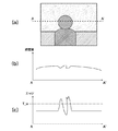
図22は、従来の撮像装置においてライブビューの際のオートフォーカス撮像動作(AF評価撮像)のタイミングを説明するための図である。 FIG. 22 is a diagram for explaining the timing of an autofocus imaging operation (AF evaluation imaging) during live view in a conventional imaging apparatus.
従来の撮像装置においては、垂直同期信号(Vertical Driving Pulse:VD)によって撮像タイミングが規定されており、AF制御信号がオンとなると、ライブビュー撮像期間後のVDに応じてAF評価像が撮像される。そして、AF制御信号がオフとなると、再びライブビュー撮像期間となる。 In a conventional imaging device, the imaging timing is defined by a vertical synchronizing signal (VD), and when the AF control signal is turned on, an AF evaluation image is captured according to VD after the live view imaging period. The When the AF control signal is turned off, the live view imaging period starts again.
このように、ライブビュー用画像を得るライブビュー撮像期間とAF評価用画像を得るAF動作期間とは時間軸に沿ってシリアルに存在するので、ライブビュー用画像とAF評価用画像を同時に撮像することはできない。 As described above, since the live view imaging period for obtaining the live view image and the AF operation period for obtaining the AF evaluation image exist serially along the time axis, the live view image and the AF evaluation image are simultaneously captured. It is not possible.
このため、図示のようにライブビュー期間(フレーム)の間に位置するAF動作期間でAF評価用画像を撮像することになって、ライブビュー用画像とAF評価用画像との間にタイムラグが存在する。加えて、AF評価用画像を撮像する際においてもライブビュー表示は行われるものの、この際には、AF評価用画像に応じてライブビュー表示が行われる。そして、図22に示すように、AF評価用画像を撮像する際には、ライブビュー撮像期間よりもフレームレートが高くされるため、撮像素子の読み出しにおいては間引き率が高くなり、不可避的に画質が低くなってしまう。 For this reason, as shown in the figure, an AF evaluation image is captured in the AF operation period located between the live view periods (frames), and there is a time lag between the live view image and the AF evaluation image. To do. In addition, although live view display is performed when an AF evaluation image is captured, live view display is performed according to the AF evaluation image. As shown in FIG. 22, when an AF evaluation image is captured, the frame rate is set higher than that of the live view imaging period. Therefore, the thinning-out rate is increased in reading of the image sensor, and the image quality is inevitably increased. It will be lower.
この点を回避するため、例えば、撮像素子の画素部に焦点信号検出用画素を撮像信号用画素とは別に設けるようにしたものがある。ここでは、ライブビュー表示のための撮像用信号を読み出すライブビュー用読み出しモードを備えるとともに、焦点検出用信号および自動露光用測光情報に用いるための撮像用信号を撮像素子から読み出す焦点検出・自動露光用読み出しモードを備えて、これら読み出しモードをフレーム毎に循環的に繰り返して行うようにしている(特許文献1参照)。 In order to avoid this point, for example, a focus signal detection pixel is provided separately from the image signal pixel in the pixel portion of the image sensor. Here, the focus detection / automatic exposure is provided with a live view readout mode for reading out an imaging signal for live view display, and reading out an imaging signal for use in a focus detection signal and photometric information for automatic exposure from an imaging device. The read mode is provided, and these read modes are cyclically repeated for each frame (see Patent Document 1).
ところが、特許文献1においては、画素単位で撮像素子から画像信号(つまり、電荷)を読み出すため、電荷の転送に時間が掛かってしまうばかりでなく、転送データ量が多くなって消費電力が増大する。さらに、撮像素子の出力である画像信号は撮像素子の外部に備えられた制御装置などによって画像信号処理されることになるので、転送データ量が多いと、制御装置における処理負荷が増大するばかりでなく、消費電力が増大する。
However, in
加えて、特許文献1においては、画素部に焦点信号検出用画素が設けられているため、不可避的に撮像信号用画素のエリアが小さくなってしまい、焦点信号検出用画素は撮像信号(画像信号)を得る際には用いられないので、画質が低下する。
In addition, in
そこで、本発明の目的は、データ転送時間を短縮するとともに画質が低下することのない撮像素子および撮像装置を提供することにある。 An object of the present invention is to provide a free imaging device and the imaging equipment of the image quality decreases with shortening the data transfer time.
上記の目的を達成するため、本発明による撮像素子は、複数の画素を備え、光学像に応じた画像信号を出力する画素部と、前記画素部を駆動する駆動手段と、前記駆動手段により前記画素部から前記画像信号が出力される出力手段と、前記出力手段に出力された前記画像信号が入力され、当該入力された前記画像信号の加算処理を行う加算手段と、前記出力手段に出力された前記画像信号が入力され、当該入力された前記画像信号に基づいて被写体のエッジ量を検出し、又は前記入力された連続する2フレームの画像信号のフレーム間の差分に基づいて前記被写体に動きがあるか否かを検出する検出手段と、前記検出手段により検出された前記被写体のエッジ量が所定量以上である場合又は前記検出手段により前記被写体に動きがあると検出された場合に前記加算手段による加算処理を行わないように制御する制御手段と、を有することを特徴とする。 In order to achieve the above object, an imaging device according to the present invention includes a plurality of pixels, a pixel unit that outputs an image signal according to an optical image, a driving unit that drives the pixel unit, and the driving unit that Output means for outputting the image signal from the pixel unit, input means for inputting the image signal output to the output means, addition processing for adding the input image signal, and output to the output means The image signal is input, and an edge amount of the subject is detected based on the input image signal, or the subject moves based on a difference between frames of the input two consecutive image signals. there is motion and detects the object by the detection means and the case edge amount of the subject detected by the detecting means is equal to or greater than a predetermined amount or said detecting means for detecting whether there is a Said control means for controlling so as not to perform addition processing by the adder means and Rukoto to have a if it.
本発明によれば、データ転送時間を短縮するとともに画質の低下を防止することができる。 According to the present invention, it is possible to prevent deterioration of image quality while shortening the data transfer time.
以下、本発明の実施の形態による撮像装置の一例について図面を参照して説明する。 Hereinafter, an example of an imaging apparatus according to an embodiment of the present invention will be described with reference to the drawings.
[第1の実施形態]
図1は、本発明の第1の実施形態による撮像装置の一例についてその構成を示すブロック図である。なお、図示の撮像装置は、例えば、動画機能付き電子スチルカメラ又はビデオカメラに適用される。
[First Embodiment]
FIG. 1 is a block diagram showing the configuration of an example of an imaging apparatus according to the first embodiment of the present invention. Note that the illustrated imaging apparatus is applied to, for example, an electronic still camera with a moving image function or a video camera.
撮像装置(以下単にカメラと呼ぶ)100は、撮影レンズユニット(以下単にレンズ部と呼ぶ)101を有しており、レンズ部101は被写体像(光学像ともいう)を撮像部103に集光する。レンズ部101には、焦点距離を変更するための焦点距離変更部および入射光を遮光するための遮光部などが含まれている。
An imaging apparatus (hereinafter simply referred to as a camera) 100 includes a photographing lens unit (hereinafter simply referred to as a lens unit) 101, and the
レンズ部101と撮像部103との間には光量調整部102が配置されており、例えば、光量調整部102は減光フィルタの挿入機構又は絞り機構である。撮像部(つまり、撮像素子)103は画素部、A/D変換回路、およびデジタル処理部(ともに図示せず)などを有している。撮像素子はレンズ部101および光量調整部102を介して結像した光学像に応じた電気信号(アナログ信号)を出力する。そして、A/D変換回路によってアナログ信号はデジタル信号(デジタル画像信号)に変換される。デジタル処理部はデジタル画像信号(以下単に画像信号とも呼ぶ)に基づいて後述する制御用の評価値を算出する。
A light
撮像部103の出力である画像信号および評価値は信号処理部104に与えられ、信号処理部104は画像信号について補正用パラメータの生成および画像信号の補正処理を行う。
The image signal and the evaluation value that are output from the
撮像制御部105は、全体制御・演算部106の制御下で、撮像部103および信号処理部104等に対してタイミング信号を送るとともに、画像信号を増幅するためのゲイン設定信号、露出時間を設定するための露出時間設定信号、およびその他の制御に必要な信号を生成する。全体制御・演算部106は撮像装置100全体の制御を司る。
The
全体制御・演算部106には、記憶部107、撮影条件検出部108、および撮影条件演算部109が備えられている。記憶部107には信号処理部104の出力である画像信号および評価値が一時的に記憶される。撮影条件検出部108は撮像部103の出力に応じて画面における被写体の位置を検出して位置情報を得る。撮影条件演算部109は、後述するようにして、位置情報に応じて撮影条件を決定する。
The overall control /
撮影条件演算部109は、決定した撮影条件に基づいてレンズ部101の焦点距離の変更、光量調整部102による光量の調整、又は撮像制御部105による露光時間およびゲインの調整を行う。
The shooting
なお、図1に示す例では、信号処理部104は全体制御・演算部106とは別の構成としたが、全体制御・演算部106が信号処理部104を備えるようにしてもよく、撮像部103に信号処理部104が備えられるようにしてもよい。
In the example shown in FIG. 1, the
図示のカメラ100には操作部110、記録部111、および表示部112が備えられており、操作部110には釦およびダイヤルなどのヒューマンIFが備えられ、ユーザ操作によって操作部110は全体制御・演算部106に各種の動作命令を行う。記録部111には、全体制御・演算部106が画像信号に応じて生成した画像データが記録される。表示部112には、全体制御・演算部105で生成された画像データに応じた画像が表示されるとともに、操作部108による入力操作に応じたアイコンなどが表示される。
The illustrated
図2は、図1に示す撮像部103に備えられた撮像素子の構成についてその一例を示すブロック図である。
FIG. 2 is a block diagram illustrating an example of the configuration of the image sensor provided in the
図2において、撮像素子は、例えば、CMOSイメージセンサであり、画素部201を有している。画素部201は2次元マトリックス状配列された複数の画素を有してする。そして、画素の各々では光電変換によって生じた電荷のリセットおよび読み出し動作が行われる。なお、画素部201には、黒信号レベルを決定するための所謂オプティカルブラック画素および回路ノイズ除去などに用いられるダミー画素が含まれている。
In FIG. 2, the image sensor is a CMOS image sensor, for example, and has a
水平信号回路202は、画素部201および垂直信号回路203aおよび203bを制御して、画素部201において各行の露光時間の設定、画素信号を読み出す読み出し行の選択および非選択設定などを行う。そして、これらの設定は全体制御・演算部106の制御下で撮像制御部105によって行われる。
The
垂直信号回路203aおよび203bの各々は、例えば、列アンプ回路、及びA/D変換回路、画素加算回路、信号メモリ、信号出力選択スイッチ、および出力回路を有している。画素部201と垂直信号回路203aおよび203bとは、列間に共通する垂直信号線で接続されている。また、ここでは、2列ごとに1つの垂直信号線が共有される。そして、垂直信号化色203aおよび203bにはそれぞれ異なる垂直信号線が交互に接続される。
Each of the
デジタル処理回路(信号処理部)204は複数の行を駆動制御して各行について独立して信号の増幅、A/D変換回路の設定(A/D変換精度、スピード、および変換ゲインなど)、画素加算の有無、および出力順の制御などを行う。 A digital processing circuit (signal processing unit) 204 drives and controls a plurality of rows, independently amplifies signals for each row, A / D conversion circuit settings (A / D conversion accuracy, speed, conversion gain, etc.), pixels Controls the presence / absence of addition and output order.
デジタル処理回路204は、垂直信号回路203aおよび203bからの出力信号に対してヘッダ情報を付加して、それぞれ外部出力バッファ205aおよび205bに出力する。図示のように、撮像素子は複数の外部出力バッファ205aおよび205bを有しているので、同時に複数の画像信号を出力することができる。
The
デジタル処理回路204には、評価値算出部206および回路条件設定部207が備えられており、評価値算出部206は撮像制御部105の制御下で、特定行の画像信号(つまり、ここでは、画素信号)から制御用の評価値を算出する。ここでは、制御用の評価値は、例えば、被写体輝度値であり、評価値算出部206は、特定行の画素信号を平均化して被写体輝度値を得る。回路条件設定部207は評価値算出部206で得られた制御用の評価値又は撮像制御部105から送られる制御信号に応じて水平信号回路202および垂直信号回路203aおよび203bの設定を行う。
The
図2に示す例では、画素部201、水平信号回路202、および垂直信号回路203aおよび203bとデジタル処理回路204および外部出力バッファ205aおよび205bとは互いに異なる基板上に形成されている。
In the example shown in FIG. 2, the
ここでは、画素部201、水平信号回路202、および垂直信号回路203aおよび203bを第1の素子部と呼び、デジタル処理回路204および外部出力バッファ205aおよび205bを第2の素子部と呼ぶ。第1および第2の素子部は、例えば、積層構造を有している。
Here, the
このようにして、多数の回路が集積するデジタル処理回路204を別の基板とすることによって、基板上の半導体面積を小さくすることができる。
In this manner, by using the
図3は、図1にカメラ100において通常の画像を取得する際のタイミングを説明するための図である。
FIG. 3 is a diagram for explaining the timing when a normal image is acquired by the
図示の例では、全体制御・演算部106又は撮像制御部105が生成する垂直同期信号に応じて、露光および信号読み出しが行われる。
In the illustrated example, exposure and signal readout are performed in accordance with a vertical synchronization signal generated by the overall control /
図4は、図2に示す撮像素子において画素部の一部分についてその構成の一例を示す図である。 FIG. 4 is a diagram illustrating an example of the configuration of a part of the pixel portion in the image sensor shown in FIG.
図示のように、ここでは、4つのフォトダイオード(PD)401によって共有構造単位408が規定される。PD401はレンズ部102を介して入射した光学像を光電変換して電荷信号(単に電荷とも呼ぶ)を出力する。転送トランジスタ(転送Tr)402は水平信号回路202から出力される転送信号(TX信号、ここではサフィックスは省略する)に応じてPD401で発生した電荷を後段に転送する。信号増幅アンプ403は、転送Tr402が導通、つまり、オンすると、PD401から転送された電荷信号を増幅する。
As shown, a shared
信号リセット用トランジスタ(リセットTr)404は、水平信号回路202から出力されるリセット信号(RS信号、ここではサフィックスは省略する)に応じてPD401および信号増幅アンプ403のリセットを行う。ここでは、図示のように、信号増幅アンプ403およびリセットTr404は4つのPD401で共有されている。
A signal reset transistor (reset Tr) 404 resets the
垂直信号線407は、信号増幅アンプ304の出力である増幅信号を垂直信号回路203a又は203bに伝送する。そして、上述の共通構造単位408を1つの単位として、複数の共通構造単位408が2次元的に配列され、TX信号およびRS信号は同一の行において、2以上の共有構造単位408に共通に接続される。
The
図5は、図2に示す水平信号回路によって行われる読み出し動作を説明するためのタイミングチャートである。 FIG. 5 is a timing chart for explaining a read operation performed by the horizontal signal circuit shown in FIG.
図3〜図5を参照して、水平信号回路202は水平同期信号に応じて、時間T501でRS信号(RS1)を立ち上げるとともに、TX信号(TX11〜TX14)を順次立ち上げる。ここでは、図示のように、TX11を立ち下げた後、時間T502でTX12を立ち上げて、RS1の立下りでTX12が立ち下げられる。
3 to 5, the
続いて、時間T503でTX11を立ち上げ、TX11を立ち下げた後、時間T504でTX12が立ち上げられる。そして、TX12を立ち下げた後、時間T505でRS1が立ち上げられるとともに、TX13が立ち上げられる。その後、TX13を立ち下げた後、時間T506でTX14が立ち上げられて、RS1の立下りでTX14が立ち下げられる。 Subsequently, TX11 is raised at time T503, TX11 is lowered, and then TX12 is raised at time T504. Then, after TX12 is lowered, RS1 is raised at time T505, and TX13 is raised. Then, after TX13 is lowered, TX14 is raised at time T506, and TX14 is lowered at the fall of RS1.
上記の動作によって、各PD401の電荷がリセットされ順次露光が行われる。そして、この動作は、撮像制御部105によって設定された条件によって、他の画素単位408においても順次行われる。
With the above operation, the charge of each
前述のように、リセット動作後において所定の露光時間が経過すると、TX11およびTX12が順次立ち上がり、各PD401の電荷が信号増幅アンプ403に順次読み出される。信号増幅アンプ403の出力である増幅信号は垂直信号線407に読み出されて、垂直信号回路203a又は203bに入力される。この動作についても、撮像制御部105によって設定された条件によって他の行で順次行われる。
As described above, when a predetermined exposure time has elapsed after the reset operation, TX11 and TX12 sequentially rise, and the charge of each
このようにして、画素のリセットおよび読み出し動作を行単位で順次行うことによって、一面(つまり、一画面)の画像信号データを取得することができる。また、動画などのように連続して撮影する場合には、垂直同期信号に同期して、撮影条件の設定を変更することができる。 In this manner, image signal data of one surface (that is, one screen) can be acquired by sequentially performing pixel reset and readout operations in units of rows. In addition, when shooting continuously such as a moving image, the setting of shooting conditions can be changed in synchronization with a vertical synchronization signal.
この撮影条件は、取得した画像信号に応じて撮影条件検出部108で行われる検出の結果に基づいて、撮影条件演算部109で算出される。そして、この撮影条件に応じて、撮像制御部105は撮像部103を制御する。なお、デジタル処理回路204は画像データを出力バッファ205aおよび205bを介して信号処理部104に出力する。
This shooting condition is calculated by the shooting
図6は、図1にカメラ100において複数の画像を同時に取得する際のタイミングを説明するための図である。
FIG. 6 is a diagram for explaining timing when a plurality of images are simultaneously acquired in the
図示の例では、全体制御・演算部106又は撮像制御部105が生成する垂直同期信号に応じて、複数の画像に関してそれぞれ露光および信号読み出しが行われる。ここでは、出力バッファ205aに出力される画像データ(メインストリーム)に対して、出力バッファ205bに出力される画像データ(サブストリーム)係るフレームレートが速くされる。
In the illustrated example, exposure and signal readout are performed for each of a plurality of images in accordance with a vertical synchronization signal generated by the overall control /
例えば、メインストリームを読み出す際の垂直同期信号よりも短い周期(ここでは、1/4の周期)でサブストリームを読み出す際の垂直同期信号を供給して、サブストリーム用の画素について露光を行い、次の垂直同期信号の期間で画像データの読み出しを行う。 For example, by supplying a vertical synchronization signal for reading a substream with a cycle shorter than the vertical synchronization signal for reading the main stream (here, a quarter cycle), the substream pixels are exposed, Image data is read out in the next vertical synchronizing signal period.
図7は、図6で説明したメインストリームおよびサブストリーム用の画素と垂直信号線に接続された垂直信号回路とを示すブロック図である。なお、垂直信号回路203aおよび203bの構成は同一である。
FIG. 7 is a block diagram showing the main stream and substream pixels described in FIG. 6 and a vertical signal circuit connected to the vertical signal line. The
図8は、図6で説明したメインストリームおよびサブストリームの読み出しのタイミングを説明するための図である。 FIG. 8 is a diagram for explaining the read timing of the main stream and the substream described in FIG.
図7および図8を参照して、垂直信号回路203bは2つの第1のスイッチ部701を有しており、これら第1のスイッチ部701はバッファ701aを介して垂直信号線407に接続される。第1のスイッチ部701はそれぞれデジタル処理回路204から与えられるSW1−1信号およびSW1−2信号によってオンオフ制御される。垂直信号線407に出力された増幅信号(OUT)は、第1のスイッチ部701の一方が時間T801でSW1−1信号によってオンすると、信号メモリ702の一方に電圧V1−1として与えられる。そして、SW1−1信号によって第1のスイッチ701の一方がオフされると(時間T802)、電圧V1−1に応じた電荷(第1の電圧信号)が信号メモリに一時的に蓄積される。
Referring to FIGS. 7 and 8, the
同様にして、SW1−2信号によって第2のスイッチ部701の他方がオンオフされて、信号メモリ702の他方に電圧V1−2に応じた電荷(第2の電圧信号)が一時的に蓄積される。このようにして、第1のスイッチ部701をオンオフ制御することによって、メインストリーム(第2の電圧信号)又はサブストリーム(第1の電圧信号)の読み出しの際に、他のストリームの読み出しなどの影響を除去することができる。
Similarly, the other of the
垂直信号回路203bは2つの第2のスイッチ部703を有しており、第2のスイッチ部703はそれぞれデジタル処理回路204から与えられるSW2−1信号およびSW2−2信号によってオンオフ制御される。信号メモリ702に蓄積された電荷は、時間T803で第1のスイッチ部703がSW2−1信号およびSW2−2信号によってオンすると、それぞれ電圧V1−1およびV1−2としてA/D変換回路704に与えられる。
The
このようにして、電圧V1−1およびV1−2をそれぞれ別のA/D変換回路704に入力することによって、撮影状態(つまり、撮影条件)に応じたA/D変換制御を行うことができる。時間T804において、A/D変換回路704は電圧(アナログ信号)V1−1およびV1−2を、デジタル処理回路204の制御下で所定のA/D変換条件に応じてデジタル信号(画像信号)D1−1およびD1−2(第1の画像データおよび第2の画像データ)に変換する。
In this way, by inputting the voltages V1-1 and V1-2 to different A /
上記の所定のA/D変換条件として、例えば、A/D変換回路の動作の有無、A/D変換におけるビット精度、A/D変換速度、A/D変換回路に対する供給電流量又は電圧、A/D変換ゲイン、およびA/D変換動作の開始時間のうち少なくとも1つがある。 Examples of the predetermined A / D conversion condition include the presence / absence of operation of the A / D conversion circuit, the bit accuracy in A / D conversion, the A / D conversion speed, the supply current amount or voltage to the A / D conversion circuit, A There is at least one of the / D conversion gain and the start time of the A / D conversion operation.
A/D変換回路704の出力である画像信号D1−1およびD1−2は出力制御部705に与えられる。そして、出力制御部705は、デジタル処理回路204の制御下で画像信号D1−1およびD1−2の少なくとも1つを選択して、時間T805において選択画像信号Doutとしてデジタル処理部204に出力する。つまり、出力制御部705は第1および第2の画像データを選択的に出力することになる。
Image signals D <b> 1-1 and D <b> 1-2 that are outputs of the A /
図9は、図7に示す出力制御部705の一例についてその構成を示すブロック図である。
FIG. 9 is a block diagram showing the configuration of an example of the
図示の出力制御部705は、第1および第2の乗算器705aおよび705bと加算器705cとを有している。そして、第1および第2の乗算器705aおよび705bにはそれぞれ画像信号D1−1およびD1−2が与えられる。第1の乗算器705aは画像信号D1−1に第1の係数αを乗算して第1の乗算信号を出力する。一方、第2の乗算器705bは画像信号D1−2に第2の係数βを乗算して第2の乗算信号を出力する。
The illustrated
加算器705は第1および第2の乗算信号を加算して、加算信号を選択画像信号として出力する。ここで、第1の係数α=0とすれば、出力制御部705から画像信号D1−1が選択画像信号として出力される。一方、第2の係数β=0とすれば、出力制御部705から画像信号D1−2が選択画像信号として出力される。また、第1の係数α=第2の係数β=1とすれば、出力制御部705から画像信号D1−1およびD1−2が選択画像信号として出力される。
The
なお、図7には示されていないが、他の垂直信号線についても、図7に示す回路構成と同様の回路構成が接続されており、複数の行について同時にA/D変換を行うことができる。 Although not shown in FIG. 7, a circuit configuration similar to the circuit configuration shown in FIG. 7 is also connected to the other vertical signal lines, and A / D conversion can be performed simultaneously on a plurality of rows. it can.
図10は、図2に示すデジタル処理回路における評価値算出部206および回路条件設定部207の接続関係を説明するためのブロック図である。
FIG. 10 is a block diagram for explaining a connection relationship between the evaluation
前述のように、デジタル処理回路204は評価値算出部206および回路条件設定部207を備えており、評価値算出部206には垂直信号回路203aおよび203bの出力である画像信号が入力される。そして、評価値算出部206は画像信号に応じて評価値を算出して、メモリ1001に当該評価値を記憶する。
As described above, the
前述の画像信号はヘッダ付加部1002にも与えられており、ヘッダ付加部1002は画像信号に同期コードおよび露出条件などのヘッダ情報を付加する。
The aforementioned image signal is also provided to the
図11は、図10に示す評価値算出部206の動作を説明するためのフローチャートである。
FIG. 11 is a flowchart for explaining the operation of the evaluation
評価値算出部206は垂直信号回路203aおよび203bからフレーム番号N=0としてサブストリームを取得する(ステップS1100)。続いて、評価値算出部206は当該サブストリームについて評価値算出対象領域(対象エリア)があるか否かを判定する(ステップS1101)。対象エリアでないと(ステップS1101において、NO)、評価値算出部206は待機する。
The evaluation
一方、対象エリアであると(ステップS1101において、YES)、評価値算出部206は評価値(制御用評価値)として被写体の輝度値Yを求める(ステップS1102)。そして、評価値算出部206は対象エリアが終了したか否かを判定する(ステップS1103)。
On the other hand, if it is the target area (YES in step S1101), the evaluation
対象エリアが終了していないと(ステップS1103において、NO)、評価値算出部206はステップS1101の処理に戻って対象エリアであるか否かを判定する。一方、対象エリアが終了すると(ステップS1103において、YES)、評価値算出部206は当該輝度値Yをメモリ1001に記憶する(ステップS1104)。
If the target area has not ended (NO in step S1103), the evaluation
続いて、評価値算出部206はフレーム番号N=N+1として(ステップS1105)、垂直信号回路203aおよび203bからサブストリームを取得する(ステップS1106)。評価値算出部206は当該サブストリームについて対象エリアがあるか否かを判定する(ステップS1107)。対象エリアでないと(ステップS1107において、NO)、評価値算出部206は待機する。
Subsequently, the evaluation
一方、対象エリアであると(ステップS1107において、YES)、評価値算出部206は評価値として被写体の輝度値Yを求める(ステップS1108)。そして、評価値算出部206は対象エリアが終了したか否かを判定する(ステップS1109)。
On the other hand, if it is the target area (YES in step S1107), the evaluation
対象エリアが終了していないと(ステップS1109において、NO)、評価値算出部206はステップS1107の処理に戻って対象エリアであるか否かを判定する。一方、対象エリアが終了すると(ステップS1109において、YES)、評価値算出部206はメモリ1001に記憶された輝度値(又は輝度平均値)とステップS1108で求めた輝度値とを平均して輝度平均値を求める(ステップS1110)。そして、評価値算出部206は当該輝度平均値をメモリ1001に記憶する(ステップS1111)。
If the target area has not ended (NO in step S1109), evaluation
続いて、評価値算出部206は、フレーム番号Nが輝度平均値を求めるための算出フレーム数(Nmax)分となったか否かを判定する(ステップS1112)。そして、N=Nmaxでないと(ステップS1112において、NO)、評価値算出部206はステップS1105に戻って次のフレームについて処理を行う。
Subsequently, the evaluation
N=Nmaxであると(ステップS1112において、YES)、評価値算出部206は算出フレーム数(Nmax)分について求めた結果(輝度平均値)Y_subを、回路条件部207に出力する(ステップS1113)。そして、評価値算出部206は評価値算出処理を終了する。
If N = Nmax (YES in step S1112), evaluation
なお、上述の例では、フレーム毎に得られた輝度値を平均化処理したが、所定の重みづけを行って最終的な輝度値を算出するようにしてもよい。さらには、フレーム間の差分を算出結果とするようにしてもよい。 In the above-described example, the luminance value obtained for each frame is averaged. However, a final luminance value may be calculated by performing predetermined weighting. Furthermore, a difference between frames may be used as a calculation result.
さらに、算出対象領域座標、算出対象領域数、および算出フレーム数(Nmax)などは、撮影制御部105から設定することができる。また、算出する輝度値を保存するメモリ1001に対して、撮影制御部105から所定の値を事前に書き込んでおくようにしてもよい。
Further, the calculation target region coordinates, the calculation target region number, the calculated frame number (Nmax), and the like can be set from the
前述のように、図示の例では、メインストリームを1枚取得する間に、サブストリームを4枚取得することができる。つまり、メインストリームを読み出す前に、少なくとも3枚のサブストリームから評価値(輝度平均値)を算出することができる。 As described above, in the illustrated example, four substreams can be acquired while one main stream is acquired. That is, an evaluation value (luminance average value) can be calculated from at least three substreams before reading the main stream.
図12は、図10に示す回路条件設定部207の動作を説明するためのフローチャートである。
FIG. 12 is a flowchart for explaining the operation of the circuit
撮影制御部105から撮影条件(つまり、第1の撮影条件)が入力されると(ステップS1201)、回路条件設定部207は水平信号回路202と垂直信号回路203aおよび230bとに撮影条件を動作設定として設定する(ステップS1202)。ここでは、回路条件設定部207はメインストリームおよびサブストリームの双方について設定を行う。
When shooting conditions (that is, the first shooting conditions) are input from the shooting control unit 105 (step S1201), the circuit
前述のようにして、評価値算出部206から算出結果Y_subが入力されると(Sステップ1203)、回路条件設定部207は、算出結果Y_subが所定の範囲にあるか否かを判定する。ここでは、回路条件設定部207は、判定下限輝度値Y_b<算出結果Y_sub<判定上限輝度値Y_uであるか否かを判定する(ステップS1204)。
As described above, when the calculation result Y_sub is input from the evaluation value calculation unit 206 (S1203), the circuit
判定の結果、Y_b<Y_sub<Y_uであると(ステップS1204において、YES)、回路条件設定部207はステップS1201の処理に戻って、再び撮影条件を入力する。一方、Y_b≧Y_sub又はY_sub≧Y_uであると(ステップS1204において、NO)、回路条件設定部207は水平信号回路202と垂直信号回路203に撮影条件(第1の撮影条件)を変更して第2の撮影条件として設定する(ステップS1205)。
As a result of the determination, if Y_b <Y_sub <Y_u (YES in step S1204), the circuit
ステップS1205の処理では、メインストリームについて水平信号回路202と垂直信号回路203aおよび203bの動作設定が行われる。例えば、回路条件設定部207は判定下限輝度値と判定上限輝度値とで規定される判定範囲からの乖離量に応じた設定値を、メインストリームを取得する際に水平信号回路202に設定されたシャッタースピード設定値から加減算する。
In the process of step S1205, the operation settings of the
なお、回路条件設定部207は判定範囲からの乖離量に応じた設定値に応じて、垂直信号回路203aおよび203bに設定されたA/D変換条件を変更するようにしてもよい。さらには、回路条件設定部207は第1のスイッチ部701の接続動作、第2のスイッチ部703の接続動作、又は出力制御部705のA/D変換結果、若しくは乗算する係数(第1および第2の係数)を変更するようにしてもよい。そして、当該動作は設定処理の終了までフレーム毎に行われる。
The circuit
続いて、回路条件設定部207は算出結果Y_subに基づいて撮影条件を変更したことを示すため、ヘッダ付加部1002によってそのヘッダに変更した撮影条件を付加する(ステップS1206)。そして、回路条件設定部207は全てのフレームについて処理を行ったか否かを判定する(ステップS1207)。
Subsequently, the circuit
全てのフレームについて処理を終了していないと(ステップS1207において、NO)、回路条件設定部207はステップS1201の処理に戻る。一方、全てのフレームについて処理を終了すると(ステップS1207において、YES)、回路条件設定部207は設定処理を終了する。
If the processing has not been completed for all frames (NO in step S1207), circuit
このようにして、本発明の第1の実施形態では、メインストリームよりもフレームレートが速いサブストリームから制御用の評価値である輝度値を算出して、当該輝度値に応じてメインストリームに係る撮影条件を変更するようにしたので、急激に被写体輝度が変化したとしても、早急に追従することができる。 Thus, in the first embodiment of the present invention, the luminance value, which is the evaluation value for control, is calculated from the substream having a frame rate faster than that of the main stream, and the main stream is related to the luminance value. Since the shooting conditions are changed, even if the subject brightness changes abruptly, it is possible to quickly follow.
なお、第1の実施形態では、画素単位408を水平2画素および垂直2画素としたが、異なる構成の画素単位においても、同様の効果を得ることができる。また、ここでは、メインストリームに用いる画素とサブストリームに用いる画素とを行単位で異ならせるようにしたが、必ずしも行単位である必要はなく、列単位で異ならせるようにしてもよい。さらには、画面内において飛び飛びの複数の画素を用いるようにしてもよい。
In the first embodiment, the
加えて、図7に示す複数のA/D変換回路は同一の形式のものでなくてもよい。つまり、第2のスイッチ部703で切り替えるようにすれば、異なる形式のA/D変換回路を用いるようにしてもよい。また、回路規模を縮小するため、第2のスイッチ部の後段に位置するA/D変換回路を共通化するようにしてもよい。この場合には、A/D変換回路は時分割で用いられることになる。
In addition, the plurality of A / D conversion circuits illustrated in FIG. 7 may not be of the same type. In other words, different types of A / D conversion circuits may be used as long as they are switched by the
第1の実施形態では、A/D変換回路は垂直信号回路203aおよび203bに備えられているが、デジタル処理回路204がA/D変換回路を備えるようにしてもよい。つまり、A/D変換回路を画素部201と異なる基板に配置するようにしてもよい。さらに、評価値算出部206はサブストリームに応じて制御用の評価値を算出するようにしたが、メインストリームに応じて評価値を算出するようにしてもよい。また、制御用の評価値である輝度値Yを算出する際には、互いに異なるカラーフィルターを用いて得られた画像信号に応じて輝度値Yを算出するようにしてもよく、カラーフィルターごとに得られた画像信号に応じて輝度値を算出するようにしてもよい。
In the first embodiment, the A / D conversion circuit is included in the
加えて、第1の実施形態では、回路条件設定部207は評価値算出部206から輝度値(輝度平均値)を受けるとしたが、輝度値をメモリ1001から取得するようにしてもよい。そして、回路条件設定部207で用いられる判定下限輝度値Y_bおよび判定上限輝度値Y_uは、全体制御演算部106から設定される。
In addition, in the first embodiment, the circuit
[第2の実施形態]
上述の第1の実施形態では、同一の画面で異なるフレームレートの複数の画像を同時に取得して、その一方の画像に応じて制御用の評価値を算出して、当該評価値に応じて他方の画像を得る際の撮影条件を変更する例について説明した。
[Second Embodiment]
In the first embodiment described above, a plurality of images with different frame rates are simultaneously acquired on the same screen, a control evaluation value is calculated according to the one image, and the other according to the evaluation value. An example of changing the shooting conditions when obtaining the image has been described.
ところが、被写体の輝度は画面内で一様ではないので、いずれの領域を評価値算出の対象エリアとするかによって、評価値が大きく異なることがある。このため、画面内のエリアに応じて撮影条件を変更した方が好ましいことがある。 However, since the luminance of the subject is not uniform within the screen, the evaluation value may vary greatly depending on which area is the target area for evaluation value calculation. For this reason, it may be preferable to change the shooting conditions according to the area in the screen.
なお、本発明の第2の実施形態におけるカメラの構成は図1に示すカメラと同様であり、さらに、画素部の構成および画像の撮影手法は第1の実施形態と同様である。 The configuration of the camera in the second embodiment of the present invention is the same as that of the camera shown in FIG. 1, and the configuration of the pixel unit and the image capturing method are the same as those of the first embodiment.
図13は、本発明の第2の実施形態によるカメラで用いられる評価値算出部206の動作を説明するためのフローチャートである。
FIG. 13 is a flowchart for explaining the operation of the evaluation
評価値算出部206は垂直信号回路203aおよび203bからフレーム番号N=0および行番号L=0としてサブストリームを取得する(ステップS1300)。続いて、評価値算出部206は当該サブストリームについて評価値算出対象領域(対象エリア)があるか否かを判定する(ステップS1301)。
The evaluation
対象エリアであると(ステップS1301において、YES)、評価値算出部206は当該行において評価値として被写体の輝度値Yを求める(ステップS1302)。そして、評価値算出部206は輝度値Yと行番号Lとをメモリ1001に保存する(ステップS1303)。
If it is the target area (YES in step S1301), the evaluation
図14は、図13に示す行単位で輝度値を算出する処理の一例を示す図である。 FIG. 14 is a diagram illustrating an example of processing for calculating a luminance value in units of rows illustrated in FIG.
図14に示すように、ここでは、算出対象領域(対象エリア)について行毎に輝度値Yが順次算出される。 As shown in FIG. 14, here, the luminance value Y is sequentially calculated for each row for the calculation target region (target area).
次に、評価値算出部206は、L=L+1として次の行に進み(ステップS1304)、対象エリアが終了したか否かを判定する(ステップS1305)。対象エリアが終了していないと(ステップS1305において、NO)、評価値算出部206はステップS1301の処理に戻って対象エリアであるか否かを判定する。なお、対象エリアでないと(ステップS1301において、NO)、評価値算出部206はステップS1304の処理に進む。
Next, the evaluation
対象エリアが終了すると(ステップS1305において、YES)、評価値算出部206はフレーム番号N=N+1として次のフレームに進み(ステップS1306)、行番号L=0としてサブストリームを取得する(ステップS1307)。評価値算出部206は当該サブストリームについて対象エリアがあるか否かを判定する(ステップS1308)。
When the target area ends (YES in step S1305), the evaluation
対象エリアであると(ステップS1308において、YES)、評価値算出部206は当該行において評価値として被写体の輝度値Yを求める(ステップS1309)。そして、評価値算出部206はメモリ1001に記憶された同一行番号Lの輝度値(又は輝度平均値)とステップS1309で求めた輝度値とを平均して輝度平均値を求める(ステップS1310)。そして、評価値算出部206は当該輝度平均値および行番号Lをメモリ1001に記憶する(ステップS1311)。
If it is the target area (YES in step S1308), the evaluation
次に、評価値算出部206は、L=L+1として次の行に進み(ステップS1312)、対象エリアが終了したか否かを判定する(ステップS1313)。対象エリアが終了していないと(ステップS1313において、NO)、評価値算出部206はステップS1308の処理に戻って対象エリアであるか否かを判定する。なお、対象エリアでないと(ステップS1308において、NO)、評価値算出部206はステップS1312の処理に進む。
Next, the evaluation
対象エリアが終了すると(ステップS1313において、YES)、評価値算出部206は、フレーム番号Nが輝度平均値を求めるための算出フレーム数(Nmax)分となったか否かを判定する(ステップS1314)。そして、N=Nmaxでないと(ステップS1314において、NO)、評価値算出部206はステップS1306に戻って次のフレームについて処理を行う。
When the target area ends (YES in step S1313), the evaluation
N=Nmaxであると(ステップS1314において、YES)、評価値算出部206は算出フレーム数(Nmax)分について求めた結果(輝度平均値)Y_sub(L)を、回路条件部207に出力する(ステップS1315)。そして、評価値算出部206は評価値算出処理を終了する。ステップS1315の処理では、各L値についてフレーム数(Nmax)分の算出結果Y_sub(L)が回路条件部207に与えられる。
If N = Nmax (YES in step S1314), evaluation
なお、上述の例では、行毎に得られた輝度値を平均化処理したが、所定の重みづけを行って最終的な輝度値を算出するようにしてもよい。さらには、フレーム間の差分を算出結果とするようにしてもよい。 In the above example, the luminance value obtained for each row is averaged, but the final luminance value may be calculated by performing predetermined weighting. Furthermore, a difference between frames may be used as a calculation result.
さらに、算出対象領域座標、算出対象領域数、および算出フレーム数(Nmax)などは、撮影制御部105から設定することができる。また、算出する輝度値を保存するメモリ1001に対して、撮影制御部105から所定の値を事前に書き込んでおくようにしてもよい。
Further, the calculation target area coordinates, the calculation target area number, the calculated frame number (Nmax), and the like can be set from the
図15は、本発明の第2の実施形態で用いられる回路条件設定部207の動作を説明するためのフローチャートである。
FIG. 15 is a flowchart for explaining the operation of the circuit
撮影制御部105から撮影条件が入力されると(ステップS1501)、回路条件設定部207は水平信号回路202と垂直信号回路203aおよび230bとに撮影条件を動作設定として設定する(ステップS1502)。ここでは、回路条件設定部207はメインストリームおよびサブストリームの双方について設定を行う。
When shooting conditions are input from the shooting control unit 105 (step S1501), the circuit
前述のようにして、評価値算出部206から算出結果Y_sub(L)が入力されると(Sステップ1503)、回路条件設定部207は、行番号L=0とする(ステップS1504)。
As described above, when the calculation result Y_sub (L) is input from the evaluation value calculation unit 206 (S1503), the circuit
続いて、回路条件設定部207は算出結果Y_sub(L)が所定の範囲にあるか否かを判定する。ここでは、回路条件設定部207は、判定下限輝度値Y_b<算出結果Y_sub(L)<判定上限輝度値Y_uであるか否かを判定する(ステップS1505)。
Subsequently, the circuit
判定の結果、Y_b<Y_sub<Y_uであると(ステップS1505において、YES)、回路条件設定部207は、後述するステップS1508の処理に進む。一方、Y_b≧Y_sub(L)又はY_sub(L)≧Y_uであると(ステップS1505において、NO)、回路条件設定部207は水平信号回路202と垂直信号回路203aおよび203bに撮影条件を変更して設定する(ステップS1506)。
As a result of the determination, if Y_b <Y_sub <Y_u (YES in step S1505), the circuit
ステップS1506の処理では、メインストリームについて水平信号回路202と垂直信号回路203aおよび203bの動作設定が行われる。例えば、回路条件設定部207は判定下限輝度値と判定上限輝度値とで規定される判定範囲からの乖離量に応じた設定値を、メインストリームを取得する際に水平信号回路202に設定されたシャッタースピード設定値から加減算する。
In the process of step S1506, operation settings of the
なお、前述のように、回路条件設定部207は判定範囲からの乖離量に応じた設定値に応じて、垂直信号回路203aおよび203bに設定されたA/D変換条件を変更するようにしてもよい。さらには、回路条件設定部207は第1のスイッチ部701の接続動作、第2のスイッチ部703の接続動作、又は出力制御部705のA/D変換結果、若しくは乗算する係数(第1および第2の係数)を変更するようにしてもよい。そして、当該動作は設定処理の終了までフレーム毎に行われる。
As described above, the circuit
続いて、回路条件設定部207は算出結果Y_sub(L)に基づいて撮影条件を変更したことを示すため、ヘッダ付加部1002によってそのヘッダに変更した撮影条件をヘッダ情報として付加する(ステップS1507)。そして、回路条件設定部207は行番号L=L+1とする(ステップS1508)。
Subsequently, in order to indicate that the imaging condition has been changed based on the calculation result Y_sub (L), the circuit
続いて、回路条件設定部207は最終行の処理を行ったか否かを判定する。つまり、回路条件設定部207は最終行に達したか否かを判定する(ステップS1509)。最終行に達しないと(ステップS1509において、NO)、回路条件設定部207はステップS1505の処理に戻って算出結果Y_sub(L)が所定の範囲にあるか否かを判定する。
Subsequently, the circuit
最終行に達すると(ステップS1509において、YES)、回路条件設定部207は全てのフレームについて処理を行ったか否かを判定する(ステップS1510)。全てのフレームについて処理を終了していないと(ステップS1510において、NO)、回路条件設定部207はステップS1501の処理に戻って撮影条件を入力する。一方、全てのフレームについて処理を終了すると(ステップS1510において、YES)、回路条件設定部207は設定処理を終了する。
When the final line is reached (YES in step S1509), circuit
このようにして、本発明の第2の実施形態では、メインストリームよりもフレームレートが速いサブストリームから制御用の評価値である輝度値を行毎に算出して、当該輝度値に応じてメインストリームに係る撮影条件を行単位で変更するようにしたので、画面内における被写体輝度の変化に対しても対処することができる。 Thus, in the second embodiment of the present invention, the luminance value, which is the evaluation value for control, is calculated for each row from the substream having a frame rate faster than that of the main stream, and the main value is determined according to the luminance value. Since the shooting conditions related to the stream are changed in units of lines, it is possible to cope with a change in subject luminance in the screen.
なお、第2の実施形態では行単位で評価値を算出するようにしたが、列単位又は飛び飛びの画素単位で評価値を算出するようにしてもよい。 In the second embodiment, the evaluation value is calculated in units of rows. However, the evaluation value may be calculated in units of columns or skipped pixels.
[第3の実施形態]
上述の第1および第2の実施形態では、制御用の評価値として輝度値を用いる例について説明した。一方、画像を取得する場合には露出条件以外にも、画面内のエリアに応じて撮影条件を変更したほうがよいことがある。なお、本発明の第3の実施形態におけるカメラの構成は図1に示すカメラと同様であり、さらに、画素部の構成および画像の撮影手法は第1および第2の実施形態と同様である。
[Third Embodiment]
In the above-described first and second embodiments, the example in which the luminance value is used as the evaluation value for control has been described. On the other hand, when acquiring an image, in addition to the exposure condition, it may be better to change the shooting condition according to the area in the screen. Note that the configuration of the camera according to the third embodiment of the present invention is the same as that of the camera shown in FIG.
図16は、本発明の第3の実施形態によるカメラで用いられるデジタル処理回路204の構成を示すブロック図である。なお、図16において、図10に示すデジタル処理回路204と同一の構成要素については同一の参照番号を付して説明を省略する。
FIG. 16 is a block diagram showing the configuration of the
図16に示すデジタル処理回路204は、画素加算部1601を有しており、画素加算部1601は撮影制御部105による設定に応じた垂直又は水平の画素データの加算処理を行う。画素データの加算によって、外部出力バッファ205から出力される画像信号のデータ量を削減することができる。また、図16に示す評価値算出部206は、制御用の評価値として被写体のエッジ量(被写体エッジ量)を検出する。
A
図17は、被写体の輝度とエッジ量との関係を示す図である。 FIG. 17 is a diagram illustrating the relationship between the luminance of the subject and the edge amount.
図17においては、画像のA−A’線で示す部分(ライン)における輝度値とエッジ量とが示されており、輝度値の変化に応じてエッジ量が変化していることが分かる。 In FIG. 17, the luminance value and the edge amount in the portion (line) indicated by the A-A ′ line of the image are shown, and it can be seen that the edge amount changes according to the change in the luminance value.
評価値算出部206は行単位で、次の式(1)に基づいて、画素加算前に対象画素(座標(x,y))の輝度値と周辺画素とのメディアン値との差分を求めて、当該差分の最大値をエッジ量T(L)とする。
The evaluation

図18は、図16に示すデジタル処理回路204における画素加算部1601の動作を説明するためのフローチャートである。
FIG. 18 is a flowchart for explaining the operation of the
撮影制御部105から撮影条件が入力されると(ステップS1801)、回路条件設定部207は撮影条件に応じて画素加算部1601に初期条件を設定する(S1802)。ここでは、回路条件設定部207はメインストリームおよびサブストリームの双方について設定を行う。
When shooting conditions are input from the shooting control unit 105 (step S1801), the circuit
評価値算出部206から行毎のエッジ量算出結果T(x,y)[以下T(L)という]が入力されると(ステップS1803)、回路条件設定部207は行番号L=0とする(ステップS1804)。そして、回路条件設定部207はエッジ量算出結果T(L)が所定の範囲にあるか否かを算出する。ここでは、回路条件設定部207はエッジ量算出結果T(L)<判定上限エッジ量T_uであるか否かを判定する(ステップS1805)。
When the edge amount calculation result T (x, y) [hereinafter referred to as T (L)] for each row is input from the evaluation value calculation unit 206 (step S1803), the circuit
判定の結果、T(L)<T_uであると(ステップS1805において、YES)、回路条件設定部207は、後述するステップS1808の処理に進む。一方、T(L)≧T_uであると(ステップS1505において、NO)、回路条件設定部207はメインストリームにおける画素加算部1601の画素加算条件を変更する設定を行う(ステップS1806)。
As a result of the determination, if T (L) <T_u (YES in step S1805), the circuit
例えば、回路条件設定部207は、エッジ量が判定上限エッジ量以上である行については当該行の画素データに関して画素加算動作を行わない設定を行う。そして、回路条件設定部207は加算条件を変更すると、その旨をヘッダ付加部1002によってヘッダ情報に付加する(ステップS1807)。
For example, the circuit
続いて、回路条件設定部207は行番号L=L+1とし(ステップS1808)、最終行に達したか否かを判定する(ステップS1809)。最終行に達しないと(ステップS1809において、NO)、回路条件設定部207はステップS1805の処理に戻ってエッジ量算出結果T(L)が所定の範囲にあるか否かを判定する。
Subsequently, the circuit
最終行に達すると(ステップS1809において、YES)、回路条件設定部207は全てのフレームについて処理を行ったか否かを判定する(ステップS1810)。全てのフレームについて処理を終了していないと(ステップS1810において、NO)、回路条件設定部207はステップS1801の処理に戻って撮影条件を入力する。一方、全てのフレームについて処理を終了すると(ステップS1810において、YES)、回路条件設定部207は設定処理を終了する。
When the final line is reached (YES in step S1809), circuit
このように、図16に示すデジタル処理回路204では、被写体情報が急激に変化するエッジ領域においては、メインストリームに係る各行についてその加算条件を変更する動作を行うこととなる。
As described above, in the
図示の例では、各行におけるエッジ量算出結果を用いる例について説明したが、複数のフレームの同一行に係るエッジ量算出結果について所定の重みづけを行うようにしてもよい。また、フレーム間の差分をエッジ量算出結果として保存するようにしてもよい。 In the illustrated example, the example using the edge amount calculation result in each row has been described. However, the edge amount calculation result related to the same row of a plurality of frames may be given a predetermined weight. Further, a difference between frames may be stored as an edge amount calculation result.
このようにして、本発明の第3の実施形態では、サブストリームに応じて、制御用の評価値であるエッジ量を行毎に求めて、当該エッジ量に応じてメインストリームに対する加算条件を行単位で変更するようにしたので、画面における被写体の変化にも適切に対処することができる。 Thus, in the third embodiment of the present invention, the edge amount, which is the evaluation value for control, is obtained for each row according to the substream, and the addition condition for the main stream is performed according to the edge amount. Since the change is made in units, it is possible to appropriately cope with changes in the subject on the screen.
なお、加算および非加算を切り替える対象およびエッジ検出の対象については、水平方向だけではなく、垂直方向も含めてもよい。さらには、第1および第2の実施形態で説明したように被写体輝度に応じて切り替えを行うようにしてもよい。 Note that the target for switching between addition and non-addition and the target for edge detection may include not only the horizontal direction but also the vertical direction. Furthermore, as described in the first and second embodiments, switching may be performed according to subject brightness.
さらに、第3の実施形態では、加算および非加算を切り替える例について説明したが、加算画素数、加算時の重み付け量、および画像信号の切り出し位置、又は加算対象画素を切り替えるようにしてもよい。 Furthermore, in the third embodiment, the example of switching between addition and non-addition has been described. However, the number of added pixels, the weighting amount at the time of addition, the cutout position of the image signal, or the addition target pixel may be switched.
加えて、上述の例では、行単位でエッジ量の判定を行うようにしたが、列単位又は画素単位でエッジ量を判定して加算条件を変更するようにしてもよい。また、評価値算出部206では評価値としてエッジ量を検出するようにしたが、評価値として動体を検出するようにしてもよい。
In addition, in the above example, the edge amount is determined in units of rows, but the addition condition may be changed by determining the edge amount in units of columns or pixels. Further, although the evaluation
図19は、図16に示す評価値算出部206で行われる動体の検出を説明するための図である。
FIG. 19 is a diagram for explaining detection of a moving object performed by the evaluation
図示の例では、評価値算出部206は、連続したサブストリームにおいてフレーム間(ここでは、第Nフレームおよび第(N−1)フレーム)で動きがあるか否かを判定する。第Nフレームと第(N−1)フレームとの間で動きがあるか否かを判定する際には、評価値算出部206は、次の式(2)に応じて第Nフレームの画像(基準画像)と第(N−1)フレームの画像との差分Diffを求める。そして、当該差分Diffが所定の差分閾値Thよりも小さいと、評価値算出部206は被写体に動き(つまり、被写体動き量)がないと判定する。一方、差分Diffが所定の差分閾値以上であると、評価値算出部206は被写体に動きがあると判定する。
In the illustrated example, the evaluation
ここで、FrN(x,y)は第Nフレーム(基準画像)の座標(x,y)における画素値であり、FrN−1(x,y)は第(N−1)フレームの座標(x,y)における画素値である。そして、これらの差分の総和を全体の差分Diffとして求める。 Here, Fr N (x, y) is a pixel value at the coordinates (x, y) of the Nth frame (reference image), and Fr N−1 (x, y) is the coordinates of the (N−1) th frame. It is a pixel value at (x, y). And the sum total of these differences is calculated | required as the whole difference Diff.
なお、上記の動体検出処理の際には、画面を少なくとも2つの領域に分割して、各領域において上述の処理を行って、領域毎に動体の有無及び方向を判定すれば、動き検出精度を向上させることができる。 In the above moving object detection process, if the screen is divided into at least two areas and the above process is performed in each area, and the presence and direction of the moving object is determined for each area, the motion detection accuracy is improved. Can be improved.
[第4の実施形態]
続いて、本発明の第4の実施形態によるカメラの一例について説明する。なお、本発明の第4の実施形態におけるカメラの構成は図1に示すカメラと同様であり、さらに、画素部の構成および画像の撮影手法は第1および第2の実施形態と同様である。
[Fourth Embodiment]
Next, an example of a camera according to the fourth embodiment of the present invention will be described. The configuration of the camera according to the fourth embodiment of the present invention is the same as that of the camera shown in FIG. 1, and the configuration of the pixel unit and the image capturing method are the same as those of the first and second embodiments.
図20は、本発明の第4の実施形態におけるカメラで用いられるデジタル処理回路204に備えられた回路条件設定部207と外部出力バッファとの接続を示すブロック図である。なお、図20に示す例において、デジタル処理回路204では回路設定部207以外の構成要素は省略されている。
FIG. 20 is a block diagram showing the connection between the circuit
図示の例では、外部出力バッファとして、メインストリーム用の外部出力バッファ205a−1および205a−2が備えられるとともに、サブストリーム用の外部出力バッファ205b−1および205b−2が備えられている。回路条件設定部207は撮影制御部105から設定される撮影条件に応じて、これら複数の外部出力バッファを選択して画像信号を出力する。つまり、回路条件設定部207はデータレートに応じて、使用する外部出力バッファの数を切り替えてその消費電力を削減する。
In the illustrated example, main output
第4の実施形態では、評価値算出部206は制御用の評価値として、例えば、エッジ量T(x,y)を算出する。そして、評価値算出部206は複数のフレーム間におけるエッジ量T(x,y)の差分T_diff(y)を回路条件設定部207に送る。差分T_diff(y)は各行におけるエッジ量T(x,y)に応じて式(3)を用いて求められる。
In the fourth embodiment, the evaluation
ここで、TN(x,y)は、第Nフレーム(基準画像)の座標(x,y)におけるエッジ量であり、TN−1(x,y)は、第(N−1)フレームの座標(x,y)におけるエッジ量である。評価値算出部206は、これら差分の総和を、対象画素数Nで割った結果を全体の差分T_diff(y)とする。
Here, T N (x, y) is the edge amount at the coordinates (x, y) of the Nth frame (reference image), and T N−1 (x, y) is the (N−1) th frame. The edge amount at the coordinates (x, y). The evaluation
図21は、図20に示す回路条件設定部207で行われる外部出力バッファの制御を説明するためのフローチャートである。
FIG. 21 is a flowchart for explaining the control of the external output buffer performed by the circuit
撮影制御部105から撮影条件が入力されると(ステップS2101)、回路条件設定部207は撮影条件に応じて外部出力バッファに係る制御条件を設定する(S2102)。ここでは、回路条件設定部207はメインストリームおよびサブストリームの双方について設定を行う。
When shooting conditions are input from the shooting control unit 105 (step S2101), the circuit
なお、上記の制御条件には、使用する外部出力バッファの数が規定されており、回路条件設定部207は制御条件に応じて、いずれの外部出力バッファに電源を供給するかについて切り替え制御を行う。
Note that the number of external output buffers to be used is defined in the above control conditions, and the circuit
評価値算出部206から行毎の差分算出結果T_diffが入力されると(ステップS2103)、回路条件設定部207は行番号L=0とする(ステップS2104)。そして、回路条件設定部207は差分算出結果T_diffが所定の範囲にあるか否かを算出する。ここでは、回路条件設定部207は差分算出結果T_diff<判定上限エッジ量T_uであるか否かを判定する(ステップS2105)。
When the difference calculation result T_diff for each row is input from the evaluation value calculation unit 206 (step S2103), the circuit
判定の結果、T_diff≧T_uであると(ステップS2105において、NO)、回路条件設定部207は、後述するステップS2108の処理に進む。一方、T_diff<T_uであると(ステップS1505において、YES)、回路条件設定部207は外部出力バッファにおける制御条件を変更する設定を行う(ステップS2106)。
As a result of the determination, if T_diff ≧ T_u (NO in step S2105), the circuit
例えば、回路条件設定部207は、メインストリーム又はサブストリームに係る外部出力バッファの制御条件を変更する。そして、回路条件設定部207は制御条件を変更した行については、前フレームと比べて被写体の変化が少ないとして、画素データの出力を行わないように外部出力バッファを制御する。回路条件設定部207は制御条件を変更すると、その旨をヘッダ付加部1002によってヘッダ情報として付加する(ステップS2107)。
For example, the circuit
続いて、回路条件設定部207は行番号L=L+1とし(ステップS2108)、最終行に達したか否かを判定する(ステップS2109)。最終行に達しないと(ステップS2109において、NO)、回路条件設定部207はステップS2105の処理に戻って差分算出結果T_diffが所定の範囲にあるか否かを判定する。
Subsequently, the circuit
最終行に達すると(ステップS2109において、YES)、回路条件設定部207は全てのフレームについて処理を行ったか否かを判定する(ステップS2110)。全てのフレームについて処理を終了していないと(ステップS2110において、NO)、回路条件設定部207はステップS2101の処理に戻って撮影条件を入力する。一方、全てのフレームについて処理を終了すると(ステップS2110において、YES)、回路条件設定部207は制御処理を終了する。
When the final line is reached (YES in step S2109), circuit
このようにして、第4の実施形態では、各行に対して上述のようにして出力制御を行って、被写体情報の変化が少ない場合は、出力データ(画像信号)のデータ量を少なくする制御を行う。 In this manner, in the fourth embodiment, output control is performed on each row as described above, and when the change in subject information is small, control is performed to reduce the data amount of output data (image signal). Do.
このように、本発明の第4の実施形態では、サブストリームから制御用の評価値を各フレーム間で算出して外部出力バッファの制御条件を行単位で変更するようにしたので、画面における被写体情報の変化に応じて消費電力を低減することができる。 As described above, in the fourth embodiment of the present invention, the control evaluation value is calculated from the substream between the frames, and the control condition of the external output buffer is changed in units of lines. Power consumption can be reduced according to changes in information.
なお、第4の実施形態においても第3の実施形態と同様に、エッジ量の検出の対象は水平方向だけではなく垂直方向も含めてもよい。第3の実施形態と同様に動体を検出して、当該検出結果に応じて外部出力バッファを制御するようにしてもよい。加えて、制御条件として、クロック周波数、供給電流又は電圧を切り替えるようにしてもよい。 In the fourth embodiment, as in the third embodiment, the detection target of the edge amount may include not only the horizontal direction but also the vertical direction. Similarly to the third embodiment, a moving object may be detected, and the external output buffer may be controlled according to the detection result. In addition, the clock frequency, supply current, or voltage may be switched as a control condition.
以上、本発明について実施の形態に基づいて説明したが、本発明は、これらの実施の形態に限定されるものではなく、この発明の要旨を逸脱しない範囲の様々な形態も本発明に含まれる。 The present invention has been described based on the embodiments. However, the present invention is not limited to these embodiments, and various forms within the scope of the present invention are also included in the present invention. .
例えば、上記の実施の形態の機能を制御方法として、この制御方法を撮像装置に実行させるようにすればよい。また、上述の実施の形態の機能を有するプログラムを制御プログラムとして、当該制御プログラムを撮像装置が備えるコンピュータに実行させるようにしてもよい。なお、制御プログラムは、例えば、コンピュータに読み取り可能な記録媒体に記録される。 For example, the function of the above embodiment may be used as a control method, and this control method may be executed by the imaging apparatus. Further, a program having the functions of the above-described embodiments may be used as a control program, and the control program may be executed by a computer included in the imaging apparatus. The control program is recorded on a computer-readable recording medium, for example.
また、本発明は、以下の処理を実行することによっても実現される。つまり、上述した実施形態の機能を実現するソフトウェア(プログラム)を、ネットワーク又は各種の記録媒体を介してシステム或いは装置に供給し、そのシステム或いは装置のコンピュータ(またはCPUやMPUなど)がプログラムを読み出して実行する処理である。 The present invention can also be realized by executing the following processing. That is, software (program) that realizes the functions of the above-described embodiments is supplied to a system or apparatus via a network or various recording media, and the computer (or CPU, MPU, etc.) of the system or apparatus reads the program. To be executed.
103 撮像部
104 信号処理部
105 撮像制御部
106 全体制御・演算部
201 画素部
202 水平信号回路
203a,203b 垂直信号回路
204 デジタル処理回路
206 評価値算出部
207 回路条件設定部
DESCRIPTION OF
Claims (8)
前記画素部を駆動する駆動手段と、
前記駆動手段により前記画素部から前記画像信号が出力される出力手段と、
前記出力手段に出力された前記画像信号が入力され、当該入力された前記画像信号の加算処理を行う加算手段と、
前記出力手段に出力された前記画像信号が入力され、当該入力された前記画像信号に基づいて被写体のエッジ量を検出し、又は前記入力された連続する2フレームの画像信号のフレーム間の差分に基づいて前記被写体に動きがあるか否かを検出する検出手段と、
前記検出手段により検出された前記被写体のエッジ量が所定量以上である場合又は前記検出手段により前記被写体に動きがあると検出された場合に前記加算手段による加算処理を行わないように制御する制御手段と、
を有することを特徴とする撮像素子。 A pixel unit that includes a plurality of pixels and outputs an image signal corresponding to the optical image;
Driving means for driving the pixel portion;
Output means for outputting the image signal from the pixel unit by the driving means;
An adding means for inputting the image signal output to the output means and performing an addition process of the input image signal;
The image signal output to the output means is input, the edge amount of the subject is detected based on the input image signal, or the difference between frames of the input two consecutive image signals is detected. Detecting means for detecting whether or not the subject is moving based on;
Control to prevent addition processing by the addition means when the edge amount of the subject detected by the detection means is greater than or equal to a predetermined amount or when the detection means detects that the subject is moving Means,
Imaging device according to claim Rukoto to have a.
前記第1の素子部と前記第2の素子部とが互いに積層されていることを特徴とする請求項1又は2に記載の撮像素子。 A first element unit including the pixel unit, the driving unit , and the output unit; and a second element unit including the addition unit, the detection unit, and the control unit.
The imaging device according to claim 1, wherein the first element portion and the second element portion are stacked on each other.
前記画素部を駆動する駆動手段と、
前記駆動手段により前記画素部から読み出された前記画像信号を撮像素子の外部に出力する外部出力手段と、
前記画像信号に基づいて被写体のエッジ量を検出する検出手段と、
前記検出手段により検出された前記被写体のエッジ量の複数のフレーム間における差分が所定量未満である場合に前記外部出力手段により出力される前記画像信号のデータ量を少なくするように制御する制御手段と、
を有することを特徴とする撮像素子。 A pixel unit that includes a plurality of pixels and outputs an image signal corresponding to the optical image;
Driving means for driving the pixel portion;
An external output means for outputting the image signal read from the pixel unit by the driving means to the outside of the image sensor;
Detecting means for detecting an edge amount of the subject based on the image signal;
Control means for controlling to reduce the data amount of the image signal output by the external output means when the difference between the plurality of frames in the edge amount of the subject detected by the detection means is less than a predetermined amount When,
An imaging device comprising:
前記制御手段は前記検出手段により検出された前記被写体のエッジ量の複数のフレーム間における差分が所定量未満である場合に前記出力バッファの数を切り替えることを特徴とする請求項4に記載の撮像素子。 The external output means comprises at least two output buffers;
5. The imaging according to claim 4, wherein the control unit switches the number of the output buffers when a difference between a plurality of frames of the edge amount of the subject detected by the detection unit is less than a predetermined amount. element.
前記第1の素子部と前記第2の素子部とが互いに積層されていることを特徴とする請求項4又は5に記載の撮像素子。 A first element unit including the pixel unit and the driving unit; and a second element unit including the external output unit, the detection unit, and the control unit.
The imaging device according to claim 4, wherein the first element portion and the second element portion are stacked on each other.
前記撮像素子から出力される前記画像信号に所定の補正処理を施す信号処理手段と、 前記撮像素子によって得られた画像を表示する表示手段と、
前記信号処理手段で得られた画像データを記録する記録手段と、
を有することを特徴とする撮像装置。 The imaging device according to any one of claims 1 to 7,
Signal processing means for performing a predetermined correction process on the image signal output from the image sensor; display means for displaying an image obtained by the image sensor;
Recording means for recording image data obtained by the signal processing means;
An imaging device comprising:
Priority Applications (1)
| Application Number | Priority Date | Filing Date | Title |
|---|---|---|---|
| JP2013136082A JP6618235B2 (en) | 2012-12-28 | 2013-06-28 | Imaging device and imaging apparatus |
Applications Claiming Priority (3)
| Application Number | Priority Date | Filing Date | Title |
|---|---|---|---|
| JP2012288036 | 2012-12-28 | ||
| JP2012288036 | 2012-12-28 | ||
| JP2013136082A JP6618235B2 (en) | 2012-12-28 | 2013-06-28 | Imaging device and imaging apparatus |
Publications (2)
| Publication Number | Publication Date |
|---|---|
| JP2014143666A JP2014143666A (en) | 2014-08-07 |
| JP6618235B2 true JP6618235B2 (en) | 2019-12-11 |
Family
ID=51424597
Family Applications (4)
| Application Number | Title | Priority Date | Filing Date |
|---|---|---|---|
| JP2013136082A Active JP6618235B2 (en) | 2012-12-28 | 2013-06-28 | Imaging device and imaging apparatus |
| JP2013136083A Pending JP2014143667A (en) | 2012-12-28 | 2013-06-28 | Imaging device, imaging apparatus, control method thereof and control program thereof |
| JP2017248092A Active JP6580118B2 (en) | 2012-12-28 | 2017-12-25 | Imaging device and imaging apparatus |
| JP2019156816A Active JP6995806B2 (en) | 2012-12-28 | 2019-08-29 | Image sensor and image sensor |
Family Applications After (3)
| Application Number | Title | Priority Date | Filing Date |
|---|---|---|---|
| JP2013136083A Pending JP2014143667A (en) | 2012-12-28 | 2013-06-28 | Imaging device, imaging apparatus, control method thereof and control program thereof |
| JP2017248092A Active JP6580118B2 (en) | 2012-12-28 | 2017-12-25 | Imaging device and imaging apparatus |
| JP2019156816A Active JP6995806B2 (en) | 2012-12-28 | 2019-08-29 | Image sensor and image sensor |
Country Status (1)
| Country | Link |
|---|---|
| JP (4) | JP6618235B2 (en) |
Families Citing this family (9)
| Publication number | Priority date | Publication date | Assignee | Title |
|---|---|---|---|---|
| JP6518503B2 (en) * | 2015-05-01 | 2019-05-22 | オリンパス株式会社 | Image pickup apparatus and control method of image pickup apparatus |
| US10148890B2 (en) | 2015-05-01 | 2018-12-04 | Olympus Corporation | Image pickup apparatus and method for controlling the same to prevent display of a through image from being stopped when a shutter unit is not completely opened |
| JP6681780B2 (en) * | 2015-05-07 | 2020-04-15 | 株式会社半導体エネルギー研究所 | Display systems and electronic devices |
| JP6727017B2 (en) * | 2016-04-21 | 2020-07-22 | キヤノン株式会社 | IMAGING DEVICE AND ITS CONTROL METHOD, IMAGE PROCESSING DEVICE, AND IMAGE PROCESSING METHOD |
| WO2018051809A1 (en) * | 2016-09-16 | 2018-03-22 | ソニーセミコンダクタソリューションズ株式会社 | Image pickup device and electronic apparatus |
| JP6762849B2 (en) * | 2016-11-08 | 2020-09-30 | キヤノン株式会社 | Image sensor, its control method, program and recording medium |
| JP6580111B2 (en) * | 2017-02-10 | 2019-09-25 | キヤノン株式会社 | Imaging device and imaging apparatus |
| CN117296334A (en) * | 2021-03-31 | 2023-12-26 | 株式会社尼康 | Image pickup element and image pickup device |
| WO2022250000A1 (en) * | 2021-05-24 | 2022-12-01 | 株式会社ニコン | Imaging element and imaging device |
Family Cites Families (27)
| Publication number | Priority date | Publication date | Assignee | Title |
|---|---|---|---|---|
| JP3394019B2 (en) * | 1990-10-08 | 2003-04-07 | オリンパス光学工業株式会社 | Exposure control circuit of image input device |
| JPH10136252A (en) * | 1996-10-31 | 1998-05-22 | Canon Inc | Image pickup device |
| JP4565370B2 (en) * | 2000-12-22 | 2010-10-20 | 富士フイルム株式会社 | Electronic camera and autofocus control method |
| JP2002300589A (en) * | 2001-01-29 | 2002-10-11 | Konica Corp | Photographing apparatus |
| JP2004146816A (en) * | 2002-09-30 | 2004-05-20 | Matsushita Electric Ind Co Ltd | Solid image pickup device and equipment using the same |
| US20050046739A1 (en) * | 2003-08-29 | 2005-03-03 | Voss James S. | System and method using light emitting diodes with an image capture device |
| JP4377840B2 (en) * | 2005-03-31 | 2009-12-02 | イーストマン コダック カンパニー | Digital camera |
| TWI429066B (en) * | 2005-06-02 | 2014-03-01 | Sony Corp | Semiconductor image sensor module and manufacturing method thereof |
| JP2007134806A (en) * | 2005-11-08 | 2007-05-31 | Canon Inc | Solid-state imaging element |
| JP2007150643A (en) * | 2005-11-28 | 2007-06-14 | Sony Corp | Solid state imaging element, driving method therefor, and imaging apparatus |
| JP2007281555A (en) * | 2006-04-03 | 2007-10-25 | Seiko Epson Corp | Imaging apparatus |
| KR101035824B1 (en) * | 2006-05-09 | 2011-05-20 | 샤프 가부시키가이샤 | Image device |
| JP2008060981A (en) * | 2006-08-31 | 2008-03-13 | Canon Inc | Image observation apparatus |
| JP2008067241A (en) * | 2006-09-11 | 2008-03-21 | Olympus Corp | Solid-state image pickup device and image pickup system |
| JP2008235478A (en) * | 2007-03-19 | 2008-10-02 | Nikon Corp | Imaging device |
| JP5022758B2 (en) * | 2007-04-12 | 2012-09-12 | キヤノン株式会社 | Imaging apparatus, imaging system, and driving method of imaging apparatus |
| JP2009021756A (en) * | 2007-07-11 | 2009-01-29 | Sony Corp | Noise rejection circuit, noise rejection method, imaging apparatus, and program |
| JP5074297B2 (en) * | 2008-05-29 | 2012-11-14 | シャープ株式会社 | Solid-state imaging device, driving method thereof, and electronic information device |
| JP5247279B2 (en) * | 2008-07-17 | 2013-07-24 | キヤノン株式会社 | Imaging apparatus, control method thereof, and program |
| JP5104812B2 (en) * | 2009-05-07 | 2012-12-19 | ソニー株式会社 | Semiconductor module |
| JP2010283787A (en) * | 2009-06-08 | 2010-12-16 | Panasonic Corp | Imaging apparatus |
| JP5537905B2 (en) * | 2009-11-10 | 2014-07-02 | 富士フイルム株式会社 | Imaging device and imaging apparatus |
| JP5452269B2 (en) * | 2010-02-10 | 2014-03-26 | オリンパス株式会社 | Imaging device |
| JP2011199716A (en) * | 2010-03-23 | 2011-10-06 | Sony Corp | Image processor, image processing method, and program |
| US8970750B2 (en) * | 2010-11-12 | 2015-03-03 | Sony Corporation | Image outputting apparatus, image outputting method, image processing apparatus, image processing method, program, data structure and imaging apparatus |
| JP2012191379A (en) * | 2011-03-10 | 2012-10-04 | Nikon Corp | Imaging apparatus |
| KR101936971B1 (en) * | 2011-03-30 | 2019-01-09 | 소니 주식회사 | A/d converter, solid-state imaging device and drive method, as well as electronic apparatus |
-
2013
- 2013-06-28 JP JP2013136082A patent/JP6618235B2/en active Active
- 2013-06-28 JP JP2013136083A patent/JP2014143667A/en active Pending
-
2017
- 2017-12-25 JP JP2017248092A patent/JP6580118B2/en active Active
-
2019
- 2019-08-29 JP JP2019156816A patent/JP6995806B2/en active Active
Also Published As
| Publication number | Publication date |
|---|---|
| JP2018057040A (en) | 2018-04-05 |
| JP6580118B2 (en) | 2019-09-25 |
| JP2014143667A (en) | 2014-08-07 |
| JP6995806B2 (en) | 2022-01-17 |
| JP2014143666A (en) | 2014-08-07 |
| JP2019201430A (en) | 2019-11-21 |
Similar Documents
| Publication | Publication Date | Title |
|---|---|---|
| JP6618235B2 (en) | Imaging device and imaging apparatus | |
| JP6172967B2 (en) | Imaging apparatus and control method thereof | |
| JP5150795B2 (en) | Imaging apparatus and imaging method | |
| KR101045892B1 (en) | Image control device and control method | |
| US20140192248A1 (en) | Imaging apparatus and method for controlling same | |
| JP6099904B2 (en) | Imaging device | |
| US10757348B2 (en) | Image pickup apparatus, image pickup apparatus control method and computer-readable non-transitory recording medium recording program | |
| JP2014154982A (en) | Image pickup device and control method therefor | |
| US10003734B2 (en) | Image capturing apparatus and control method of image sensor | |
| JP2007097085A (en) | Digital camera | |
| JP2020036128A (en) | Imaging device and control method therefor, program, storage medium | |
| US8169494B2 (en) | Image sensing apparatus and method of controlling image sensing apparatus | |
| JP2013236298A (en) | Imaging apparatus | |
| JP5452269B2 (en) | Imaging device | |
| JP7258465B2 (en) | Imaging device and its control method | |
| KR20120133142A (en) | A digital photographing apparatus, a method for auto-focusing, and a computer-readable storage medium for executing the method | |
| JP7234015B2 (en) | Imaging device and its control method | |
| JP2019041170A (en) | Imaging apparatus and control method of the same | |
| JP7252730B2 (en) | IMAGING CONTROL DEVICE AND IMAGE SENSOR DRIVING METHOD | |
| JP2007088842A (en) | Imaging apparatus, and method of driving imaging device | |
| JP7292962B2 (en) | Imaging device and its control method | |
| JP7309420B2 (en) | Imaging device | |
| JP2014007454A (en) | Image pickup device and image pickup method | |
| JP6393087B2 (en) | Imaging device and imaging apparatus | |
| US20230199342A1 (en) | Imaging device and imaging method |
Legal Events
| Date | Code | Title | Description |
|---|---|---|---|
| A621 | Written request for application examination |
Free format text: JAPANESE INTERMEDIATE CODE: A621 Effective date: 20160610 |
|
| A977 | Report on retrieval |
Free format text: JAPANESE INTERMEDIATE CODE: A971007 Effective date: 20170314 |
|
| A131 | Notification of reasons for refusal |
Free format text: JAPANESE INTERMEDIATE CODE: A131 Effective date: 20170411 |
|
| A521 | Request for written amendment filed |
Free format text: JAPANESE INTERMEDIATE CODE: A523 Effective date: 20170607 |
|
| A131 | Notification of reasons for refusal |
Free format text: JAPANESE INTERMEDIATE CODE: A131 Effective date: 20170725 |
|
| A521 | Request for written amendment filed |
Free format text: JAPANESE INTERMEDIATE CODE: A523 Effective date: 20170921 |
|
| A02 | Decision of refusal |
Free format text: JAPANESE INTERMEDIATE CODE: A02 Effective date: 20171003 |
|
| A521 | Request for written amendment filed |
Free format text: JAPANESE INTERMEDIATE CODE: A523 Effective date: 20171225 |
|
| A911 | Transfer to examiner for re-examination before appeal (zenchi) |
Free format text: JAPANESE INTERMEDIATE CODE: A911 Effective date: 20180111 |
|
| A912 | Re-examination (zenchi) completed and case transferred to appeal board |
Free format text: JAPANESE INTERMEDIATE CODE: A912 Effective date: 20180126 |
|
| A521 | Request for written amendment filed |
Free format text: JAPANESE INTERMEDIATE CODE: A523 Effective date: 20190306 |
|
| A521 | Request for written amendment filed |
Free format text: JAPANESE INTERMEDIATE CODE: A523 Effective date: 20190516 |
|
| A61 | First payment of annual fees (during grant procedure) |
Free format text: JAPANESE INTERMEDIATE CODE: A61 Effective date: 20191112 |
|
| R151 | Written notification of patent or utility model registration |
Ref document number: 6618235 Country of ref document: JP Free format text: JAPANESE INTERMEDIATE CODE: R151 |