JP2014143667A - Imaging device, imaging apparatus, control method thereof and control program thereof - Google Patents
Imaging device, imaging apparatus, control method thereof and control program thereof Download PDFInfo
- Publication number
- JP2014143667A JP2014143667A JP2013136083A JP2013136083A JP2014143667A JP 2014143667 A JP2014143667 A JP 2014143667A JP 2013136083 A JP2013136083 A JP 2013136083A JP 2013136083 A JP2013136083 A JP 2013136083A JP 2014143667 A JP2014143667 A JP 2014143667A
- Authority
- JP
- Japan
- Prior art keywords
- control
- image
- imaging
- signal
- unit
- Prior art date
- Legal status (The legal status is an assumption and is not a legal conclusion. Google has not performed a legal analysis and makes no representation as to the accuracy of the status listed.)
- Pending
Links
Images


Landscapes
- Transforming Light Signals Into Electric Signals (AREA)
- Studio Devices (AREA)
- Exposure Control For Cameras (AREA)
- Focusing (AREA)
- Automatic Focus Adjustment (AREA)
- Solid State Image Pick-Up Elements (AREA)
- Stroboscope Apparatuses (AREA)
Abstract
Description
本発明は、積層構造を有する撮像素子、当該撮像素子を備える撮像装置、その制御方法、および制御プログラムに関し、特に、画像信号に応じて測光測距などに係る評価値を検出することのできる撮像装置に関する。 The present invention relates to an image pickup device having a laminated structure, an image pickup apparatus including the image pickup device, a control method thereof, and a control program, and in particular, an image pickup capable of detecting an evaluation value related to photometric distance measurement according to an image signal. Relates to the device.
撮像装置により撮像された信号を用いて画像評価及び画像表示を行う技術がある。特許文献1では、ライブビュー表示のための撮像用信号を読み出すライブビュー用読み出しモードを備えるとともに、焦点検出用信号および自動露光用測光情報に用いるための撮像用信号を撮像素子から読み出す焦点検出・自動露光用読み出しモードを備えている。そして、これら読み出しモードをフレーム毎に循環的に繰り返して行っている。
There is a technique for performing image evaluation and image display using a signal imaged by an imaging device. In
ところが、特許文献1においては、画素単位で撮像素子から画像信号(つまり、電荷)を読み出すため、電荷の転送に時間が掛かってしまうばかりでなく、転送データ量が多くなって消費電力が増大する。
However, in
さらに、撮像素子の出力である画像信号は別の制御装置などによって画像信号処理されることになるので、転送データ量が多いと、制御装置における処理負荷が増大してしまう。 Furthermore, since the image signal that is the output of the image sensor is subjected to image signal processing by another control device or the like, if the amount of transfer data is large, the processing load on the control device increases.
加えて、特許文献1においては、画素部に焦点信号検出用画素が設けられているため、不可避的に撮像信号用画素のエリアが小さくなってしまい、焦点信号検出用画素は撮像信号(画像信号)を得る際には用いられないので、画質が低下する。
In addition, in
そこで、本発明の目的は、データ転送時間を短縮するとともに画質が低下することを抑えた撮像素子、撮像装置、その制御方法、および制御プログラムを提供することにある。 SUMMARY OF THE INVENTION An object of the present invention is to provide an imaging device, an imaging apparatus, a control method thereof, and a control program that can shorten the data transfer time and suppress the deterioration of the image quality.
上記目的を達成するため、本発明による撮像素子は、光学像が結像され、前記光学像に応じた画像信号を出力する撮像素子であって、マトリックス状に配列された複数の画素を有し、前記光学像に応じた電圧信号を出力する第1の素子部と、前記電圧信号をデジタル信号に変換して前記画像信号を得る第2の素子部とを備え、前記第2の素子部は、前記複数の画素のうちの第1の画素群から得られる電圧信号に応じた前記画像信号を第1の画像信号として前記第1の画像信号に応じて撮像の際に用いられる制御情報を生成する制御情報生成部と、前記複数の画素のうち第2の画素群から得られる電圧信号に応じた前記画像信号を第2の画像信号として前記第2の画像信号を画像表示のための画像表示信号として出力する出力手段とを有することを特徴とする。 In order to achieve the above object, an image sensor according to the present invention is an image sensor that forms an optical image and outputs an image signal corresponding to the optical image, and has a plurality of pixels arranged in a matrix. A first element unit that outputs a voltage signal corresponding to the optical image, and a second element unit that converts the voltage signal into a digital signal to obtain the image signal, and the second element unit includes: And generating control information used in imaging according to the first image signal, using the image signal corresponding to the voltage signal obtained from the first pixel group of the plurality of pixels as the first image signal. A control information generation unit that performs image display for displaying the second image signal as the second image signal, the image signal corresponding to the voltage signal obtained from the second pixel group among the plurality of pixels. Output means for outputting as a signal. The features.
本発明による撮像装置は、上記の撮像素子と、前記制御情報を受けて当該制御情報に応じて撮像の際の制御を行う制御手段と、前記画像表示信号に応じてライブビュー表示を行う表示制御手段と、を有することを特徴とする。 An image pickup apparatus according to the present invention includes the above-described image pickup device, a control unit that receives the control information and performs control in imaging according to the control information, and display control that performs live view display according to the image display signal. And means.
本発明による制御方法は、上記の撮像素子を備える撮像装置の制御方法であって、前記制御情報を受けて当該制御情報に応じて撮像の際の制御を行う制御ステップと、前記画像表示信号に応じてライブビュー表示を行う表示制御ステップと、を有することを特徴とする。 A control method according to the present invention is a method for controlling an image pickup apparatus including the above-described image pickup device, and includes a control step of receiving the control information and performing control in imaging according to the control information, and the image display signal. And a display control step for performing live view display accordingly.
本発明による制御プログラムは、上記の撮像素子を備える撮像装置で用いられる制御プログラムであって、前記撮像装置が備えるコンピュータに、前記制御情報を受けて当該制御情報に応じて撮像の際の制御を行う制御ステップと、前記画像表示信号に応じてライブビュー表示を行う表示制御ステップと、を実行させることを特徴とする。 A control program according to the present invention is a control program used in an imaging apparatus including the above-described imaging device, and receives control information from a computer included in the imaging apparatus and performs control during imaging according to the control information. And a display control step of performing live view display in accordance with the image display signal.
本発明によれば、フォーカス制御などの制御を行う際、当該制御のみに用いられる制御情報を撮像素子から出力するようにしたので、データ転送時間を短縮して、しかも画質の低下を回避することができる。 According to the present invention, when control such as focus control is performed, the control information used only for the control is output from the image sensor, so that the data transfer time is shortened and the deterioration of the image quality is avoided. Can do.
以下、本発明の実施の形態による撮像装置の一例について図面を参照して説明する。 Hereinafter, an example of an imaging apparatus according to an embodiment of the present invention will be described with reference to the drawings.
[第1の実施形態]
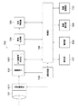
図1は、本発明の第1の実施形態による撮像装置の一例についてその構成を示すブロック図である。
[First Embodiment]
FIG. 1 is a block diagram showing the configuration of an example of an imaging apparatus according to the first embodiment of the present invention.
図示の撮像装置は、例えば、動画機能付き電子スチルカメラ又はビデオカメラに適用される。 The illustrated imaging apparatus is applied to, for example, an electronic still camera or a video camera with a moving image function.
撮像装置100は、光学鏡筒101、撮像素子102、駆動回路103、信号処理部104、圧縮伸長部105、制御部106、発光部107、操作部108、画像表示部109、および画像記録部110を有している。
The
光学鏡筒101は、レンズユニット(図示せず、以下単にレンズと呼ぶ)および光学機構部1011を備えている。レンズは被写体からの光(光学像)を撮像素子102に集光する(つまり、結像する)。
The
図示はしないが、光学機構部1011はAF機構、ズーム駆動機構、メカニカルシャッタ機構、および絞り機構など有している。そして、光学機構部1011は制御部106から制御下で駆動回路103によって駆動される。
Although not shown, the
撮像素子102は、後述する画素部201およびA/Dコンバータ(図示せず)を有し、例えば、所謂XY読み出し方式のCMOS型イメージセンサである。そして、撮像素子102は制御部106の制御下で動作する駆動回路103によって、露光、信号読み出し、およびリセットなどの撮像動作を行って、撮像信号(画像信号ともいう)を出力する。
The
撮像素子102には、AF評価値検出部1021が備えられており、このAF評価値検出部1021は撮像素子102で得られる画像信号に応じて得られるコントラスト情報および位相差情報に基づいて、制御部106で制御されるタイミングでAF評価値(オートフォーカス評価値)を検出する。そして、AF評価値検出部1021は当該AF評価値を制御部106に出力する。
The
信号処理部104は、制御部106の制御下で、撮像素子102の出力である画像信号に対して、ホワイトバランス調整処理、色補正処理、およびAE(Auto Exposure)処理などの信号処理を施して画像データとして出力する。
The
圧縮伸長部105は、制御部106の制御下で動作し、信号処理部104の出力である画像データに対して、JPEG(Joint Photographic Coding Experts Group)方式などの所定の静止画像データフォーマットによって圧縮符号化処理を行う。また、圧縮伸長部105は制御部106から送られた符号化画像データを伸長復号化処理する。
The compression /
なお、圧縮伸長部105は、MPEG(Moving Picture Experts Group)方式などによって動画像データについて圧縮符号化/伸長復号化処理を行うようにしてもよい。
Note that the compression /
制御部106は、例えば、CPU(Central Processing Unit)、ROM(Read Only Memory)、およびRAM(Random Access Memory)などを備えるマイクロコントローラである。そして、CPUがROMに記憶されたプログラムを実行することによって、撮像装置100全体を統括的に制御する。
The
発光部107は、信号処理部104によるAE処理によって被写体の露光値が低いと判定されると、被写体に対して光を照射して照明を行う。発光部107として、例えば、キセノン管を用いたストロボ装置又はLED発光装置が用いられる。
If the
操作部108は、例えば、シャッタレリーズボタンなどの各種操作キー、レバー、およびダイヤルを有し、ユーザの入力操作に応じた操作信号を制御部106に与える。
The
画像表示部109は、例えば、LCD(Liquid Crystal Display)などの表示デバイスおよびLCDに対するインタフェース回路を備え、制御部106から送られた画像データに応じた画像を表示デバイスに表示する。
The
画像記録部110は、例えば、可搬型の半導体メモリ、光ディスク、HDD(Hard Disk Drive)、又は磁気テープなどの記録媒体であり、圧縮伸長部105により圧縮符号化された画像データを画像ファイルとして記憶する。また、画像記録部110は制御部106によって指定された画像ファイルを読み出して制御部106に出力する。
The
ここで、図1に示す撮像装置100の基本的な動作について説明する。
Here, a basic operation of the
例えば、静止画像を撮影する際には、その撮像前において、撮像素子102では画素201から出力された画像信号を順次CDS処理およびAGC処理を施した後、A/Dコンバータでデジタル画像信号に変換される。そして、このデジタル画像信号はAF評価検出部1021および信号処理部104に出力される。
For example, when capturing a still image, the
AF評価値検出部1021は、デジタル画像信号から得られるコントラスト情報に応じてAF評価値(制御情報)を算出して、当該AF評価値を制御部106に出力する。制御部106はAF評価値に基づいて光学機構部1011の制御量を決定し、この制御量に応じて駆動回路103を制御する。これによって、光学機構部1011が駆動回路103によって駆動される。
The AF evaluation
信号処理部104は、上記のデジタル画像信号に対して、例えば、画質補正処理を施してカメラスルー画像信号を生成して、当該カメラスルー信号を制御部106を介して画像表示部108に送る。これによって、画像表示部108はカメラスルー画像信号に応じたカメラスルー画像を表示し、ユーザはカメラスルー画像を目視しつつ画角合わせを行うことができる。
The
この状態で、操作部108のシャッタレリーズボタンが押下されると、制御部106の制御によって、撮像素子102からの1フレーム分の撮像信号(デジタル画像信号)が信号処理部104に取り込まれる。信号処理部104は当該1フレーム分のデジタル画像信号に画質補正処理を施して、処理後のデジタル画像信号(画像データ)を圧縮伸長部105に送る。
In this state, when the shutter release button of the
圧縮伸長部105は画像データ圧縮符号化して、符号化画像データを制御部106を介して画像記録部110に送る。これによって、撮像された静止画像に係る画像ファイルが画像記録部110に記録される。
The compression /
画像記録部110に記録された画像ファイルを再生する際には、制御部106は、操作部108からの操作入力に応じて選択された画像ファイルを画像記録部110から読み込む。そして、制御部106は当該画像ファイルを圧縮伸長部105に送って、圧縮伸長部105に伸長復号化処理を実行させる。
When playing back an image file recorded in the
復号化された画像データは制御部106を介して画像表示部109に送られる。これによって、画像表示部109には画総データに応じた静止画像が再生表示される。
The decoded image data is sent to the
動画像データを記録する際には、制御部106の制御によって撮像素子102から出力されたデジタル画像信号が信号処理部104に取り込まれる。信号処理部104において順次処理された画像データは圧縮伸長部105で圧縮符号化処理される。そして、圧縮伸長部105から符号化動画像データが順次画像記録部110に転送されて動画像ファイルとして記録される。
When recording moving image data, a digital image signal output from the
画像記録部110に記録された動画像ファイルを再生する際には、制御部106は、操作部108からの操作入力に応じて、選択された動画像ファイルを画像記録部110から読み込む。そして、制御部106は当該動画像ファイルを圧縮伸長部105に送って、圧縮伸長部105に伸長復号化処理を実行させる。復号化された動画像データは制御部106を介して画像表示部109に送られる。これによって、画像表示部109には動画像データに応じた動画像が再生表示される。
When playing back a moving image file recorded in the
ここで、従来の撮像装置における撮像画像から評価値を算出しつつ、表示画像を表示する技術とその課題について説明する。従来、撮像装置においてフォーカス制御に用いる被写体の位置情報を得る際には、撮像素子から出力される画像信号に応じて当該位置情報を得ている。また、被写体を示す光信号を専用の検出装置に直接入力して、当該光信号が示す画像における位相差に応じて位置情報を得ることも行われている。そして、画像信号に応じて位置情報を得る場合には、専用の検出装置が不要となる点で、撮像装置を小型化することができる。 Here, a technique for displaying a display image while calculating an evaluation value from a captured image in a conventional imaging apparatus and its problem will be described. Conventionally, when obtaining position information of a subject used for focus control in an image pickup apparatus, the position information is obtained according to an image signal output from an image pickup device. In addition, an optical signal indicating a subject is directly input to a dedicated detection device, and position information is obtained according to a phase difference in an image indicated by the optical signal. And when obtaining positional information according to the image signal, the imaging device can be miniaturized in that a dedicated detection device is not required.
図10は、従来の撮像装置においてライブビューの際のオートフォーカス撮像動作(AF評価撮像)のタイミングを説明するための図である。 FIG. 10 is a diagram for explaining the timing of autofocus imaging operation (AF evaluation imaging) during live view in a conventional imaging apparatus.
従来の撮像装置においては、垂直同期信号(Vertical Driving Pulse:VD)によって撮像タイミングが規定されており、AF制御信号がオンとなると、ライブビュー撮像期間後のVDに応じてAF評価像が撮像される。そして、AF制御信号がオフとなると、再びライブビュー撮像期間となる。 In a conventional imaging device, imaging timing is defined by a vertical synchronizing signal (Vertical Driving Pulse: VD). When the AF control signal is turned on, an AF evaluation image is captured according to VD after the live view imaging period. The When the AF control signal is turned off, the live view imaging period starts again.
このように、ライブビュー用画像を得るライブビュー撮像期間とAF評価用画像を得るAF動作期間とは時間軸に沿ってシリアルに存在するので、ライブビュー用画像とAF評価用画像を同時に撮像することはできない。 As described above, since the live view imaging period for obtaining the live view image and the AF operation period for obtaining the AF evaluation image exist serially along the time axis, the live view image and the AF evaluation image are simultaneously captured. It is not possible.
このため、図示のようにライブビュー期間(フレーム)の間に位置するAF動作期間でAF評価用画像を撮像することになって、ライブビュー用画像とAF評価用画像との間にタイムラグが存在する。 For this reason, as shown in the figure, an AF evaluation image is captured in the AF operation period located between the live view periods (frames), and there is a time lag between the live view image and the AF evaluation image. To do.
加えて、AF評価用画像を撮像する際においてもライブビュー表示は行われるものの、この際には、AF評価用画像に応じてライブビュー表示が行われる。そして、図10に示すように、AF評価用画像を撮像する際には、ライブビュー撮像期間よりもフレームレートが高くされるため、撮像素子の読み出しにおいては間引き率が高くなり、不可避的に画質が低くなってしまう。この点を回避するため、例えば、撮像素子の画素部に焦点信号検出用画素を撮像信号用画素とは別に設けるようにしたものもある。 In addition, although live view display is performed when an AF evaluation image is captured, live view display is performed according to the AF evaluation image. As shown in FIG. 10, when the AF evaluation image is captured, the frame rate is set higher than that of the live view imaging period. Therefore, the thinning rate is increased in reading of the image sensor, and the image quality is inevitably increased. It will be lower. In order to avoid this point, for example, a focus signal detection pixel may be provided separately from the image signal pixel in the pixel portion of the image sensor.
本実施形態では、上記課題に鑑み、図2に示すような撮像素子102の構成をもって、画像信号から得られる評価値あるいは評価値に基づく制御情報を表示用の画像信号と並行して生成し、処理時間の短縮および処理負荷の軽減を図る。
In the present embodiment, in view of the above problem, with the configuration of the
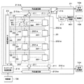
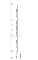
図2は、図1に示す撮像素子102の構成を説明するための図である。そして、図2(a)はその構造を示す斜視図であり、図2(b)はその構成を示すブロック図である。
FIG. 2 is a diagram for explaining the configuration of the
図2(a)において、撮像素子102は第1のチップ(画素部)20および第2のチップ21を有しており、第2のチップ(第2の素子部)21上に第1のチップ(第1の素子部)20が積層されている。第1のチップ20はマトリックス状に配列された複数の画素201を有しており、第1のチップ20は光入射側に配置されている(つまり、光学像の受光側に位置している)。
In FIG. 2A, the
第2のチップ21は後述する列走査回路213−aおよび213−bと行走査回路212などの画素駆動回路が形成されるとともに、前述のAF評価値検出部(制御情報生成部)1021が形成されている。
In the
このように、第1のチップ20に画素201を形成し、第2のチップ21に画素駆動回路およびAF評価値検出部1021を形成すれば、撮像素子102の周辺回路および画素部の製造プロセスを分けることができ、周辺回路における配線の細線化、高密度化による高速化、小型化、および高機能化を図ることができる。
As described above, if the
図2(b)に示すように、第1のチップ20において、画素201はマトリクス状に配列されており、画素201は水平方向(行方向)において転送信号線203、リセット信号線204、および行選択信号線205に接続され、垂直方向(列方向)において列信号線202−aおよび202−bに接続されている。なお、列信号線202−aおよび202−bの各々は読み出し行単位に応じて接続先が異なる。
As shown in FIG. 2B, in the
図示のように、画素201の各々は、光電変換素子であるフォトダイオードPD、転送トランジスタM1、リセットトランジスタM2、増幅トランジスタM3、選択トランジスタM4、フローティングディフュージョンFDを有している。
As illustrated, each of the
なお、図示の例では、トランジスタの各々はnチャネルMOSFET(MOS Field−Effect Transistor)である。 In the illustrated example, each of the transistors is an n-channel MOSFET (MOS Field-Effect Transistor).
転送トランジスタM1、リセットトランジスタM2、および選択トランジスタM4のゲートには、それぞれ転送信号線203、リセット信号線204、および行選択信号線205が接続されている。これら信号線203〜205は水平方向に延在し、同一行の画素が同時に駆動される。これによってライン順次動作型のローリングシャッタの動作を制御して、所定の行毎に露出時間を変えて撮像することができる。又は全行同時動作型のグローバルシャッタの動作を制御することができる。
A
さらに、選択トランジスタM4のソースには列信号線202−a又は202−bが行単位で接続されている。 Further, the column signal line 202-a or 202-b is connected to the source of the selection transistor M4 in units of rows.
フォトダイオードPDは、光電変換によって生成された電荷を蓄積する。そして、フォトダイオードPDのP側が接地され、N側が転送トランジスタM1のソースに接続されている。転送トランジスタM1がオンすると、フォトダイオードPDの電荷がFDに転送され、FDには寄生容量が存在するので、FDに転送された電荷が蓄積される。 The photodiode PD accumulates electric charges generated by photoelectric conversion. The P side of the photodiode PD is grounded, and the N side is connected to the source of the transfer transistor M1. When the transfer transistor M1 is turned on, the charge of the photodiode PD is transferred to the FD, and since there is a parasitic capacitance in the FD, the charge transferred to the FD is accumulated.
増幅トランジスタM3のドレインには電源電圧Vddが印加され、そのゲートはFDに接続されている。増幅トランジスタM3は、FDの電荷(つまり、電圧)を増幅して電圧信号に変換する。選択トランジスタM4は、信号を読み出す画素を行単位で選択するためのものであり、そのドレインは増幅トランジスタM3のソースに接続されている。また、選択トランジスタM4のソースは列信号線202に接続されている。
A power supply voltage Vdd is applied to the drain of the amplification transistor M3, and its gate is connected to the FD. The amplification transistor M3 amplifies the charge (that is, voltage) of the FD and converts it into a voltage signal. The selection transistor M4 is for selecting a pixel from which a signal is read out in units of rows, and its drain is connected to the source of the amplification transistor M3. The source of the selection transistor M4 is connected to the
選択トランジスタM4がオンすると、FDの電圧に対応する電圧信号が列信号線202に出力される。リセットトランジスタM2のドレインには電源電圧Vddが印加され、そのソースはFDに接続されている。リセットトランジスタM2のオンによって、FDの電圧は電源電圧Vddにリセットされる。
When the selection transistor M4 is turned on, a voltage signal corresponding to the voltage of the FD is output to the
第2のチップ21には、カラムADCブロック211が備えられており、カラムADC211は列信号線202−a又は202−bに接続されている。さらに、第2のチップ21には、行走査回路212、列走査回路213−aおよび213−b、タイミング制御回路214、水平信号線(出力手段)215−aおよび215−b、切替スイッチ216、フレームメモリ217、およびAF評価値検出部1021が備えられている。
The
タイミング制御回路214は制御部106の制御下で行走査回路212、列走査回路213−aおよび213−b、およびカラムADCブロック211の動作タイミングを制御する。行走査回路212は各行の走査を行い、列走査回路213aおよび213bはそれぞれ各列の走査を行う。
The
水平信号線215−aおよび215−bは、それぞれ列走査回路213−aおよび213−bで制御されるタイミングに応じてカラムADCブロック211の出力信号(画像信号)を転送する。 The horizontal signal lines 215-a and 215-b transfer the output signal (image signal) of the column ADC block 211 according to the timing controlled by the column scanning circuits 213-a and 213-b, respectively.
フレームメモリ217は水平信号線215−bから出力される画像信号を一時的に記憶する。AF評価値検出部1021はフレームメモリ217に記憶された画像信号に応じてAF評価値して、当該AF評価値を制御部106に送る。
The
切替スイッチ216は水平信号線215−bに出力される画像信号をAF評価値検出部1021および信号処理部104のいずれか一方に選択的に出力するためのスイッチである。
The
なお、水平信号線215−aに転送された画像信号は信号処理部104に与えられる。
The image signal transferred to the horizontal signal line 215-a is given to the
図3は、図2に示す第1のチップ20において列信号線202−a又は202−bにおける画素選択を説明するための図である。
FIG. 3 is a diagram for explaining pixel selection in the column signal line 202-a or 202-b in the
図3においては、6行×8列の画素部が示されており、ここでは各画素はベイヤ配列されている。 In FIG. 3, a pixel portion of 6 rows × 8 columns is shown, and here, each pixel is arranged in a Bayer array.
図1に示す操作部108の操作によってフォーカス制御モードになると、制御部106はライブビュー用撮像(第2の撮像モード)およびAF評価値検出用撮像(第1の撮像モード)を同時に行うことができるように、撮像素子102における読み出し行を分ける(つまり、切替スイッチ216を切替制御して、水平信号線215−bをフレームメモリ217に接続する)。
When the focus control mode is set by the operation of the
これによって、ライブビュー用の画像信号(第2の画像信号、つまり、画像表示信号)は列信号線202−aに出力され、AF評価検出用の画像信号(第1の画像信号)は列信号線202−bに出力される。 Thereby, an image signal for live view (second image signal, that is, an image display signal) is output to the column signal line 202-a, and an image signal for AF evaluation detection (first image signal) is a column signal. Output to line 202-b.
図3において、行番号1および2はAF評価値検出用撮像のための行(第1の画素群)であり、行番号3〜8はライブビュー用撮像のための行(第2の画素群)である。図示の例では、読み出し走査が行単位で順次行われて、8行単位で繰り返し読み出し走査が行われることになる。
In FIG. 3,
AF評価値検出用撮像では、フレームレート重視のため垂直同色4画素中3画素(4ライン中3ライン)を間引き読み出しする。一方、ライブビュー用撮像では、画質重視のため、残りの垂直同色4画素中1画素(4ライン中1ライン)を間引き3画素を加算する。 In AF evaluation value detection imaging, 3 out of 4 pixels of the same vertical color (3 lines out of 4 lines) are read out by thinning out the frame rate. On the other hand, in live view imaging, in order to emphasize image quality, 1 pixel out of the remaining 4 pixels of the same color (1 line out of 4 lines) is added with 3 pixels thinned out.
言い換えると、AF評価値検出用撮像においては、第1の画素群を第1のフレームレートで読み出しを行う。そして、ライブビュー用撮像では第2の画素群を第1のフレームレートよりも遅い第2のフレームレートで読み出しを行う。 In other words, in the AF evaluation value detection imaging, the first pixel group is read at the first frame rate. In live view imaging, the second pixel group is read out at a second frame rate that is slower than the first frame rate.
上述のように、選択行毎にAF走査用撮像とライブビュー用撮像とを分けることによって、異なる電荷蓄積時間でデータサイズの異なるフレームレートの画像信号を取得することが可能となる。 As described above, by dividing AF scanning imaging and live view imaging for each selected row, it is possible to acquire image signals of different frame rates with different data sizes in different charge accumulation times.
次に列信号線202−aおよび202−bに出力された電圧信号(アナログ信号)は、図2に示すカラムADCブロック211においてアナログ信号からデジタル信号(画像信号)に変換される。 Next, the voltage signals (analog signals) output to the column signal lines 202-a and 202-b are converted from analog signals to digital signals (image signals) in the column ADC block 211 shown in FIG.
カラムADCブロック211の出力である画像信号は、列走査回路213−a又は213−bによってカラムADCブロック211から水平信号線215−a又は215−bに読み出される。水平信号線215−aに読み出された画像信号は信号処理部104に送られる。
The image signal which is the output of the column ADC block 211 is read from the column ADC block 211 to the horizontal signal line 215-a or 215-b by the column scanning circuit 213-a or 213-b. The image signal read out to the horizontal signal line 215-a is sent to the
一方、水平信号線215−bに読み出された画像信号は、スイッチ216に出力され、制御部106の制御に応じて信号処理部104又はフレームメモリ217に出力される。なお、切替スイッチ216による切り替えはフレーム単位で行われる。
On the other hand, the image signal read to the horizontal signal line 215-b is output to the
このとき、静止画などの撮影では間引くことなく画素信号を読み出すことから、スイッチ216は信号処理部104に繋ぐ経路にスイッチする。
At this time, since the pixel signal is read out without being thinned out when shooting a still image or the like, the
一方、AF評価モード(つまり、オートフォーカス制御モード)の際には、水平信号線215−bから切替スイッチ216を介してフレームメモリ217に画像信号が記録され、AF評価値検出部1021はフレームメモリ217に記録された画像信号におけるコントラスト情報に基づいてAF評価値を検出する。AF評価値は被写体のフォーカス情報として、コントラスト情報、もしくは光学機構部1011内のAF機構部におけるデフォーカス移動量やAF機構部の制御情報で構成され、多画素のAF評価値用画像データと比較すると、データ量として十分に小さい。このAF評価値はAF評価値検出部1021から制御部106に送られる。
On the other hand, in the AF evaluation mode (that is, the autofocus control mode), an image signal is recorded in the
このように、本実施形態においてAF評価値検出部1021がチップ21内に組み込まれているのは、省電力と高速処理、低コスト設計のためである。チップ21と、信号処理部104もしくは制御部106は、それぞれ別基板などに配置されることが多く、チップ間の通信に当たっては配線の抵抗成分や容量成分が多くなる。そのため、同一チップ内の配線による通信に比べて低速になるか、高速な信号を送出するには信号波形品質を保つためアンプで駆動する必要があるなど、駆動電力を上げなければならない。
As described above, the AF evaluation
一方、同一半導体チップ上にAF評価値検出部1021があることで画像データの出力配線が短く済み、アンプの配置も省ける。加えて、AF評価値自体もデータ量が少ないため、撮像素子102と制御部106との通信時間が短くなるため、消費電力の低下を図ることができる。
On the other hand, since the AF evaluation
以下の説明では、撮像の際、列信号線202−aおよび水平信号線215−aによる出力経路をチャンネルCh1と呼び、列信号線202−bおよび水平信号線215−bによる出力経路をチャンネルCh2と呼ぶ。 In the following description, during imaging, the output path by the column signal line 202-a and the horizontal signal line 215-a is called a channel Ch1, and the output path by the column signal line 202-b and the horizontal signal line 215-b is a channel Ch2. Call it.
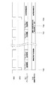
図4は、図1に示すカメラ100におけるAF評価モードの際の撮像タイミングを説明するためのタイミング図である。
FIG. 4 is a timing chart for explaining the imaging timing in the AF evaluation mode in the
図示のように、垂直同期信号(VD)によって撮像タイミングが規定されており、AF評価モードとなると、制御部106は時間T0の垂直同期信号VDの立下りでAF制御信号、チャンネルCh1を用いたライブビュー撮像とチャンネルCh2を用いたAF評価用撮像とを同時に開始する。
As shown in the figure, the imaging timing is defined by the vertical synchronization signal (VD), and in the AF evaluation mode, the
期間T0〜TF1で、チャンネルCh2を介して画素部20から読み出されたAF評価用画像信号は、水平信号線215−bおよび切替スイッチ216を介してフレームメモリ217に保存される。そして、期間TF1〜TF2において、AF評価値検出部1021はフレームメモリ217に保存されたAF用画像信号に応じてAF評価値を算出する。その後、期間TF2〜TF3において、AF評価値検出部1021はAF評価値を制御部106に出力する。
In the period T0 to TF1, the AF evaluation image signal read from the
図示の例では、1垂直同期信号VDの期間中にライブビューが1フレーム分撮像され、AF評価(AF走査)が3フレーム分撮像される。そして、制御部106が垂直同期信号VDをLレベルとすると(時間T1)、AF評価が終了する。
In the illustrated example, the live view is imaged for one frame during the period of one vertical synchronization signal VD, and AF evaluation (AF scanning) is imaged for three frames. Then, when the
上記のように、図1に示すカメラ100では、AF評価モードの際に、信号処理部104を介して画像データを制御部106に送ってAF評価値を得る必要がないので、つまり、データ容量の少ないAF評価値を撮像素子102から直接制御部106に出力するようにしたので、負荷低減による電力削減を行うことができる。
As described above, in the
制御部106はAF評価値と後述する所定のAF期待値とを比較して、AF評価値がAF期待値を満足すると、AF制御信号を立ち下げる(時間T1)。AF制御信号が立ち下がると、AF評価用撮像のみが停止して、ライブビュー撮像が継続して行われることになる。
The
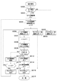
図5は、図1に示すカメラ100における制御を説明するためのフローチャートである。なお、図示のフローチャートは制御部106の制御下で行われる。
FIG. 5 is a flowchart for explaining control in the
カメラ100の電源がオンとされてスタンバイ状態(つまり、撮像前の撮像準備状態)になると、制御部106はAF評価モードであるか否かを判定する(ステップS502)。つまり、制御部106はオートフォーカスモードが設定されているか否かを判定する。
When the power source of the
AF評価モードでないと(ステップS502において、NO)、制御部106はライブビュー撮像を開始して(ステップS503)、後述のステップS515に進む。
If it is not the AF evaluation mode (NO in step S502), the
一方、AF評価モードであると(ステップS502において、YES)、制御部106はAF制御信号をオン(Hレベル)とする(ステップSONにする(ステップS504)。続いて、制御部106はAF評価用撮像回数をカウントするための変数nに0を代入する(ステップS505)。
On the other hand, in the AF evaluation mode (YES in step S502),
次に、図4で説明したようにして、制御部106はAF評価用撮像を開始するとともに(ステップS506)、ステップS516においてライブビュー用撮像を開始する。
Next, as described with reference to FIG. 4, the
AF評価用撮像を開始した後、制御部106は変数nを1インクリメントする(ステップS507)。その後、制御部106の制御下で、AF評価値検出部1021はAF評価用撮像によって得られたAF評価用画像信号に応じてAF評価値AF_Kを検出する(ステップS508)。
After starting the AF evaluation imaging, the
続いて、制御部106は、AF評価値AF_KがAF期待値であるK_minおよびK_maxに対して次の式(1)、つまり、所定の評価条件を満たすか否かを判定する(ステップS509)。
Subsequently, the
K_min<AF_K<K_max (1)
ここでAF期待値K_minおよびK_maxは期待されるAF評価値の最小値および最大値を示しており、予めカメラ100の設計の際又はカメラ100の調整の際に制御部106に記録される。
K_min <AF_K <K_max (1)
Here, the expected AF values K_min and K_max indicate the minimum and maximum expected AF evaluation values, and are recorded in the
AF評価値AF_Kが式(1)を満たさないと(ステップS509において、NO)、制御部106は上記のAF評価値AF_Kに応じてフィードバック制御量を求める。そして、制御部106は当該フィードバック制御量に応じて駆動回路103を駆動制御して光学機構部1011に備えられたフォーカスレンズを光軸に沿って駆動する(ステップS510)。
If the AF evaluation value AF_K does not satisfy the expression (1) (NO in step S509), the
続いて、制御部106は変数(AF評価値撮像回数)nが所定の数(ここでは、3)であるか否かを判定する(ステップS511)。AF評価値撮像回数が3回未満であれば(ステップS511において、NO)、制御部106はステップS506の処理に戻ってAF評価用撮像を行う。
Subsequently, the
一方、AF評価値撮像回数が3回であれば(ステップS511において、YES)、制御部106はライブビュー表示を行った後(ステップS512)、ステップS505の処理に戻ってAF評価値撮像回数nをゼロとする。
On the other hand, if the number of AF evaluation value imaging is 3 (YES in step S511),
AF評価値AF_Kが式(1)を満たすと(ステップS509において、YES)、制御部106はAF制御信号をオフ(Lレベル)として(ステップS513)、撮像素子102におけるAF評価用撮像を停止する(ステップS514)。そして、制御部106は撮像したライブビュー用画像信号に応じた画像を画像表示部109に表示して(ステップS515)、待機状態となる(ステップS517)。
When the AF evaluation value AF_K satisfies Expression (1) (YES in step S509), the
なお、図5に示すフローチャートでは、制御部106はAF評価用撮像を停止した後、ステップS516のライブビュー用撮像によって得られた画像信号に応じた画像を表示することになる。また、ステップS503のライブビュー用撮像を開始すると、制御部106はステップS515の処理に進んで、ライブビュー表示を行う。
In the flowchart illustrated in FIG. 5, the
上述のように、本発明の第1の実施形態では、第2のチップ21内にAF評価値検出部1021を備え、ライブビュー用画像の撮像と並行して、フレームレートの速いAF評価用画像の撮像とAF評価値を算出して出力することができる。これにより、AF評価を行う際のタイムラグを短縮することができる。
As described above, in the first embodiment of the present invention, the AF evaluation
また、AF評価の際には、データ容量の少ないAF評価値のみが撮像素子102から直接制御部106に送られるので、信号出力負荷が軽減されて消費電力を削減することができる。
In AF evaluation, only an AF evaluation value having a small data capacity is directly sent from the
なお、上述の実施形態ではライブビューの際にAFを行う例について説明したが、ライブビューに限らずその他動画撮影の際においても上記の手法を用いることができる。 In the above-described embodiment, an example in which AF is performed at the time of live view has been described. However, the above method can be used not only at live view but also at the time of moving image shooting.
また、ここでは、AF評価値を撮像素子102から制御部106に直接出力して、制御部106がAF評価値に応じて駆動回路103によって光学機構部1011を制御するようにしたが、駆動回路103がAF評価値に応じて光学機構部1011を駆動制御するようにしてもよい。
Here, the AF evaluation value is directly output from the
[第2の実施形態]
次に、本発明の第2の実施形態によるカメラの一例について説明する。
[Second Embodiment]
Next, an example of a camera according to the second embodiment of the present invention will be described.
なお、第2の実施形態によるカメラの構成は図1に示すカメラと同様であるが、撮像素子102の構成が図2(b)に示す撮像素子と異なる。また、以下の説明では、ストロボなどの発光部による測光動作の際の静止画撮影について説明する。
The configuration of the camera according to the second embodiment is the same as that of the camera shown in FIG. 1, but the configuration of the
図6は、本発明の第2の実施形態によるカメラで用いられる撮像素子の一例についてその構成を示すブロック図である。 FIG. 6 is a block diagram showing the configuration of an example of an image sensor used in the camera according to the second embodiment of the present invention.
なお、図6において、図2(a)に示す撮像素子と同一の構成要素については同一の参照番号を付して説明を省略する。 In FIG. 6, the same components as those in the image sensor shown in FIG.
図6に示す撮像素子102では、第2のチップ21はAF評価値用検出部1021の代わりに測光値評価部601を備えており、この測光値評価部601はフレームメモリ217に接続されるとともに、制御部106に接続されている。
In the
測光値評価部601は、第1のチップ20から列信号線202−bおよび水平信号線215b(つまり、チャンネルCh2)を介して読み出された画像信号に応じて色比率および露光値を測光値として算出する。そして、測光評価部601は当該測光値に応じてホワイトバランス係数および発光部107の発光制御量などの測光制御データを制御部106に出力する。
The photometric
制御部106は測光制御データに応じて信号処理部104および発光部107に制御命令を送って、信号処理部104におけるホワイトバランス補正および発光部107の発光量を制御する。
The
図7は、本発明の第2の実施形態における測光評価モードの際の撮像タイミングを説明するためのタイミング図である。 FIG. 7 is a timing chart for explaining the imaging timing in the photometric evaluation mode in the second embodiment of the present invention.
測光評価モードとなると、制御部106は時間T70の垂直同期信号VDの立下りで垂直同期信号VDに同期してチャンネルCh1を用いたライブビュー撮像とチャンネルCh2を用いた測光評価用撮像とを同時に開始する。この測光評価用撮像においては、ホワイトバランス係数および発光部107の発光制御のための測光評価用撮像が行われる。
In the photometric evaluation mode, the
ここでは、ホワイトバランス係数算出のための測光評価用撮像をホワイトバランス係数算出用撮像と呼び、発光制御のための測光評価用撮像を発光制御量測光用撮像と呼ぶ。 Here, photometry evaluation imaging for white balance coefficient calculation is called white balance coefficient calculation imaging, and photometry evaluation imaging for light emission control is called light emission control amount photometry imaging.
まず、期間T70〜T71において、ホワイトバランス係数算出用撮像が行われて、チャンネルCh2を介して画素部20から読み出されたホワイトバランス係数評価用画像信号は、水平信号線215−bおよび切替スイッチ216を介してフレームメモリ217に保存される。
First, in a period T70 to T71, white balance coefficient calculation imaging is performed, and the white balance coefficient evaluation image signal read from the
そして、期間T71〜T72において、測光値評価部601はフレームメモリ217に保存されたホワイトバランス係数評価用画像信号に応じてホワイトバランス係数を算出する。その後、期間T72〜T73において、測光値評価部601はホワイトバランス係数を制御部106に出力する。
In periods T71 to T72, the photometric
続いて、時間T73において、制御部106は発光制御信号を立ち上げて(Hレベル)、発光部107を所定の発光量で発光させながら、発光制御量測光用撮像を開始する。そして、時間T74において、制御部106は発光制御信号を立ち下げて(Lレベル)、発光制御量測光用撮像を停止する。
Subsequently, at time T73, the
これによって、期間T73〜T74において、静止画撮影の際における発光部107の発光制御量測光用撮像が行われて、発光制御量評価用画像信号がフレームメモリ217に保存される。
Thus, during the period T73 to T74, the light emission control amount photometric imaging of the
なお、期間T73〜T74においては、発光制御信号がオンとなるので、発光部107による事前発光(つまり、プリ発光)が行われて、被写体の露光量を算出するための撮像である発光制御量測光用撮像が行われることになる。
Note that, during the periods T73 to T74, since the light emission control signal is turned on, the light emission control amount that is imaging for calculating the exposure amount of the subject by performing pre-light emission (that is, pre-light emission) by the
期間T74〜T75において、測光値評価部601はフレームメモリ217に保存された発光制御量評価用画像信号に応じて被写体に係る露光値を算出して、当該露光値に応じて発光制御量を生成する。続いて、期間T75〜T76において、測光値評価部601は発光制御量制御部106に出力する。
In periods T74 to T75, the photometric
時間T76において、制御部106は測光評価モードを静止画撮影モードに切り替えるとともに、発光制御信号をオンとして発光部109を発光させる(本発光)。この際、制御部106は発光制御量に応じて発光部107の発光量を制御する。
At time T76, the
さらに、制御部106は切替スイッチ216を切り替えて、チャンネルCh2を介して出力される画像信号を信号処理部104に出力して、画素部20の全画素から読み出された画像信号を信号処理部104に与える。
Furthermore, the
図示の例では、1垂直同期信号VDの期間中にライブビューが1フレーム分撮像され、この間にホワイトバランス係数算出用撮像およびホワイトバランス係数の算出・出力と発光制御量測光用撮像および発光制御量の算出・出力が行われる。 In the example shown in the figure, during the period of one vertical synchronization signal VD, one frame of live view is imaged. During this period, white balance coefficient calculation imaging, white balance coefficient calculation / output, emission control amount metering imaging, and emission control are performed. A quantity is calculated and output.
このように、本発明の第2の実施形態では、第2のチップ21内にAF評価値検出部1021を備え、ライブビュー用画像の撮像と並行して、フレームレートの速い測光評価用画像の撮像と測光評価値を算出して出力することができる。これにより、測光評価を行う際のタイムラグを短縮することができる。
As described above, in the second embodiment of the present invention, the AF evaluation
また、測光評価の際には、データ容量の少ない測光評価値(ホワイトバランス係数および発光制御量)のみが撮像素子102から直接制御部106に送られるので、信号出力負荷が軽減されて消費電力を削減することができる。
In the photometric evaluation, only the photometric evaluation values (white balance coefficient and light emission control amount) with a small data volume are sent directly from the
なお、上述の実施形態では測光評価値を撮像素子102から制御部106に直接出力して、制御部106が測光評価値に応じて信号処理部104および発光部107を制御するようにしたが、撮像素子102から測光評価値を信号処理部104および発光部107に送って直接的に制御するようにしてもよい。
In the above-described embodiment, the photometric evaluation value is directly output from the
[第3の実施形態]
続いて、本発明の第3の実施形態によるカメラの一例について説明する。
[Third Embodiment]
Next, an example of a camera according to the third embodiment of the present invention will be described.
なお、第3の実施形態によるカメラの構成は図1に示すカメラと同様であるが、撮像素子102の構成が図2(b)に示す撮像素子と異なる。
The configuration of the camera according to the third embodiment is the same as that of the camera shown in FIG. 1, but the configuration of the
図8は、本発明の第3の実施形態によるカメラで用いられる撮像素子の一例についてその構成を示すブロック図である。 FIG. 8 is a block diagram showing the configuration of an example of an image sensor used in the camera according to the third embodiment of the present invention.
なお、図8において、図2(a)および図6に示す撮像素子と同一の構成要素については同一の参照番号を付して説明を省略する。 In FIG. 8, the same components as those of the image sensor shown in FIG. 2A and FIG.
図8に示す撮像素子102では、第2のチップ21はAF評価値用検出部1021の代わりに画像信号評価部801を備えており、この画像信号評価部801はフレームメモリ217に接続されるとともに、制御部106に接続されている。
In the
画像信号評価部801は、第1のチップ20から列信号線202−bを介して読み出された画像信号に応じて信号ばらつきを示す標準偏差(標準偏差値ともいう)を算出する。そして、画像信号評価部801は当該標準偏差を画像信号評価値として制御部106に出力する。制御部106は標準偏差が予め設定された閾値(標準偏差閾値)を超えると、ゲインアップ量又は露光量(つまり、露光期間)を抑える撮像制御信号を駆動回路103に送る。駆動回路103はこの撮像制御信号に応じて撮像素子102を駆動して露出制御を行う。標準偏差が予め設定された閾値を超えると、画像信号におけるS/N比が悪化していることになり、所定の画質を保つためには、露出制御に制限をかけるとよいからである。
The image
図8に示す例では、露出制御によって所定の画質を保つようにしたが、露出制御に限らず、例えば、ノイズリダクション処理における補正値を切り替えて所定の画質を保つようにしてもよい。さらに、図示の例では、画像信号評価部801は標準偏差である画像信号評価値を出力するようにしたが、画像信号評価部801は駆動回路103、信号処理部104、又は発光部107に標準偏差に応じた制御信号を出力して所定の画質を保つようにしてもよい。
In the example shown in FIG. 8, the predetermined image quality is maintained by the exposure control. However, the present invention is not limited to the exposure control, and for example, the correction value in the noise reduction process may be switched to maintain the predetermined image quality. Furthermore, in the illustrated example, the image
図9は、本発明の第3の実施形態における標準偏差評価モードの際の撮像タイミングを説明するためのタイミング図である。 FIG. 9 is a timing chart for explaining the imaging timing in the standard deviation evaluation mode in the third embodiment of the present invention.
標準偏差評価モードとなると、制御部106は時間T90において垂直同期信号VD1およびVD2の立下りで撮像を開始する。ここでは、制御部106は垂直同期信号VD1に同期してチャンネルCh1を用いたライブビュー撮像と、垂直同期信号VD2に同期してチャンネルCh2を用いた標準偏差評価用撮像(画像信号評価用撮像ともいう)とを開始する。
When the standard deviation evaluation mode is entered, the
なお、垂直同期信号VD1に同期したライブビュー撮像においては、ライブビュー表示のためのフレームレートに応じて撮像動作が行われ、垂直同期信号VD2に係る1VD期間(T90〜T93)の間に複数フレームのライブビュー撮像が行われることになる。 Note that in live view imaging synchronized with the vertical synchronization signal VD1, an imaging operation is performed according to the frame rate for live view display, and a plurality of frames are generated during the 1VD period (T90 to T93) related to the vertical synchronization signal VD2. Live view imaging will be performed.
期間T90〜T91における画像信号評価用撮像において、チャンネルCh2に読み出された標準偏差検出用画像信号が撮像素子102から読み出されるが、この期間T90〜T91は、時間T93以降における静止画撮像における露出期間と同一の設定となる。時間T93以降の露出制御については、操作部108を用いたユーザ操作又は撮像素子102から得られる画像信号に応じたAE制御に応じて決定される。よって、チャンネルCh2における画像信号評価用撮像においてはチャンネルCh1におけるライブビュー表示とは異なる露出制御となる。
In the image signal evaluation imaging in the periods T90 to T91, the standard deviation detection image signal read to the channel Ch2 is read from the
さらに、チャンネルCh2において、時間T93以降の静止画撮影と同様の露出制御をすることによって、静止画撮影前に画質の悪化要因となる信号増幅によるS/Nの悪化、そして、撮像画素の長秒蓄積動作などの撮像制御に制限をかけることができる。その結果、静止画の画質が所定のレベル以上に悪化することを防止することができる。 Further, in channel Ch2, exposure control similar to still image shooting after time T93 is performed, so that S / N deterioration due to signal amplification that causes image quality deterioration before still image shooting, and a long period of imaging pixels It is possible to limit imaging control such as accumulation operation. As a result, it is possible to prevent the image quality of the still image from deteriorating beyond a predetermined level.
期間T90〜T91において撮像の結果得られたチャンネルCh2の出力、つまり、標準偏差検出用画像信号は、水平信号線215−bおよびスイッチ216を介してフレームメモリ217に保存される。そして、期間T91〜T92において、フレームメモリ217に保存された標準偏差検出用画像信号は画像信号評価部801に読み出されて、画像信号評価部801は標準偏差検出用画像信号について信号ばらつきである標準偏差値を算出する。
The output of the channel Ch2 obtained as a result of imaging in the periods T90 to T91, that is, the standard deviation detection image signal is stored in the
その後、期間T92〜T93において、画像信号評価部801は期間T91〜T92で算出された標準偏差値のみを撮像素子102から制御部106に出力する。時間T93以降においては、カメラは標準偏差評価モードから静止画撮影モードに切り替わり、制御部106はスイッチ216を切り替えて画像信号を信号処理104に出力可能な状態として、全画素の読み出しができるようにする。この際、制御部106は画像信号評価部801で算出された標準偏差値に応じて露光制御を行う。
Thereafter, in the periods T92 to T93, the image
上述のように、本発明の第3の実施形態では、ライブビュー用画像信号と評価用の画像信号とを同時に撮像するようにしたので、静止画の撮像を行う前に静止画撮像における動作を制御するための標準偏差値を実際の撮影前に検出することができる。 As described above, in the third embodiment of the present invention, the image signal for live view and the image signal for evaluation are imaged at the same time. Therefore, the operation in the still image capturing is performed before the still image capturing. The standard deviation value for control can be detected before actual photographing.
さらに、第3の実施形態では、データ量が少ない画像信号評価値である標準偏差値を直接制御部106に出力するようにしたので、撮像素子102から信号処理部104にデータ量が大きい画像信号を送る必要がなくなる。この結果、信号出力に起因する負荷低減によって電力削減を行うことができる。
Furthermore, in the third embodiment, since the standard deviation value, which is an image signal evaluation value with a small amount of data, is directly output to the
このようにして、本発明の第3の実施形態では、ライブビュー用の撮像とは別にライブビューとは異なる撮像期間で画像信号を撮像素子102において同時に取得して、当該画像信号に応じて画像信号評価値である標準偏差値を撮像素子102で算出して制御部106に出力する。これによって、ライブビュー中に画像信号評価値が得られて、省電力とともに時間短縮を図ることができる。
As described above, in the third embodiment of the present invention, image signals are simultaneously acquired by the
なお、第3の実施形態では、画像信号に係る標準偏差値を求める例について説明したが、次のような評価値を画像信号評価部801で算出させて、対応する補正を制御部106に行わせてもよい。
In the third embodiment, an example in which the standard deviation value related to the image signal is obtained has been described. However, the following evaluation value is calculated by the image
(1)画像信号基準値となるオフセット成分の1フレームあたりの変動量を画像信号から算出する画像信号オフセット補正値の算出、(2)列もしくは行単位での筋状となる固定パターンノイズの検出、(3)動画録画やライブビュー表示とは別の露出条件を設定し、光源出力の変化を検知することによるフリッカ検出、(4)WB係数、(5)対象被写体の移動量、(6)ベクトル量を検知することによる手ぶれ補正値もしくは被写体の動き検出値の算出、(7)色シェーディング評価値、(8)輝度シェーディング評価値、(9)フリッカ評価値を求めて、光学機構部1011内の絞り機構部や撮像素子102のシャッタ制御による露光制御を行うようにしてもよい。
(1) Calculation of an image signal offset correction value for calculating a fluctuation amount per frame of an offset component serving as an image signal reference value from the image signal, (2) Detection of fixed pattern noise that forms a streak in columns or rows. (3) Flicker detection by setting a different exposure condition from moving image recording and live view display and detecting a change in light source output, (4) WB coefficient, (5) amount of movement of the subject, (6) By calculating a camera shake correction value or a subject motion detection value by detecting a vector amount, (7) a color shading evaluation value, (8) a luminance shading evaluation value, and (9) a flicker evaluation value are obtained. Exposure control by shutter control of the aperture mechanism unit or the
なお、上記各評価値の取得方法と補正方法については上記しているものの他に公知の手法を用いることももちろん可能である。 In addition to the above-described methods, it is of course possible to use known methods for obtaining and correcting each evaluation value.
上述の説明から明らかなように、図1に示す例では、制御部106および駆動回路103が制御手段および読み出し制御手段として機能する。また、制御部106および画像表示部109は表示制御手段として機能する。
As is apparent from the above description, in the example shown in FIG. 1, the
以上、本発明について実施の形態に基づいて説明したが、本発明は、これらの実施の形態に限定されるものではなく、この発明の要旨を逸脱しない範囲の様々な形態も本発明に含まれる。 As mentioned above, although this invention was demonstrated based on embodiment, this invention is not limited to these embodiment, Various forms of the range which does not deviate from the summary of this invention are also contained in this invention. .
例えば、上記の実施の形態の機能を制御方法として、この制御方法を撮像装置に実行させるようにすればよい。また、上述の実施の形態の機能を有するプログラムを制御プログラムとして、当該制御プログラムを撮像装置が備えるコンピュータに実行させるようにしてもよい。なお、制御プログラムは、例えば、コンピュータに読み取り可能な記録媒体に記録される。 For example, the function of the above embodiment may be used as a control method, and this control method may be executed by the imaging apparatus. Further, a program having the functions of the above-described embodiments may be used as a control program, and the control program may be executed by a computer included in the imaging apparatus. The control program is recorded on a computer-readable recording medium, for example.
上記の制御方法および制御プログラムの各々は、少なくとも制御ステップおよび表示制御ステップを有している。 Each of the above control method and control program has at least a control step and a display control step.
また、本発明は、以下の処理を実行することによっても実現される。つまり、上述した実施形態の機能を実現するソフトウェア(プログラム)を、ネットワーク又は各種の記録媒体を介してシステム或いは装置に供給し、そのシステム或いは装置のコンピュータ(またはCPUやMPUなど)がプログラムを読み出して実行する処理である。 The present invention can also be realized by executing the following processing. That is, software (program) that realizes the functions of the above-described embodiments is supplied to a system or apparatus via a network or various recording media, and the computer (or CPU, MPU, etc.) of the system or apparatus reads the program. To be executed.
102 撮像素子
104 信号処理部
106 制御部
212 行走査回路
213 列走査回路
216 切替スイッチ
217 フレームメモリ
601 測光値評価部
801 画像信号評価部
1021 AF評価値検出部
DESCRIPTION OF
Claims (17)
マトリックス状に配列された複数の画素を有し、前記光学像に応じた電圧信号を出力する第1の素子部と、
前記電圧信号をデジタル信号に変換して前記画像信号を得る第2の素子部とを備え、
前記第2の素子部は、前記複数の画素のうちの第1の画素群から得られる電圧信号に応じた前記画像信号を第1の画像信号として前記第1の画像信号に応じて撮像の際に用いられる制御情報を生成する制御情報生成部と、
前記複数の画素のうち第2の画素群から得られる電圧信号に応じた前記画像信号を第2の画像信号として前記第2の画像信号を画像表示のための画像表示信号として出力する出力手段とを有することを特徴とする撮像素子。 An image sensor that forms an optical image and outputs an image signal corresponding to the optical image,
A first element unit that has a plurality of pixels arranged in a matrix and outputs a voltage signal corresponding to the optical image;
A second element unit that converts the voltage signal into a digital signal to obtain the image signal;
The second element section captures the image signal corresponding to the voltage signal obtained from the first pixel group of the plurality of pixels as the first image signal according to the first image signal. A control information generator for generating control information used for
Output means for outputting the image signal corresponding to a voltage signal obtained from a second pixel group among the plurality of pixels as a second image signal and the second image signal as an image display signal for image display; An image pickup device comprising:
前記第1の素子部が前記光学像を受光する側に位置していることを特徴とする請求項1又は2に記載の撮像素子。 The first element part and the second element part are stacked and arranged,
The imaging device according to claim 1, wherein the first element unit is located on a side that receives the optical image.
前記撮像を行う前の撮像準備状態において前記スイッチ手段は前記第1の画像信号を前記制御情報生成部に与えることを特徴とする請求項1〜3のいずれか1項に記載の撮像素子。 The second element unit includes switch means for selectively supplying the first image signal to the control information generation unit,
4. The image sensor according to claim 1, wherein the switch unit supplies the first image signal to the control information generation unit in an imaging preparation state before the imaging is performed. 5.
前記出力手段は前記第1の画像信号および前記第2の画像信号を撮像信号として出力することを特徴とする請求項4に記載の撮像素子。 When the imaging is performed, the switch means gives the first image signal to the output means,
The imaging device according to claim 4, wherein the output means outputs the first image signal and the second image signal as imaging signals.
前記制御情報を受けて当該制御情報に応じて撮像の際の制御を行う制御手段と、
前記画像表示信号に応じてライブビュー表示を行う表示制御手段と、
を有することを特徴とする撮像装置。 The image sensor according to any one of claims 1 to 5,
Control means for receiving the control information and performing control upon imaging according to the control information;
Display control means for performing live view display according to the image display signal;
An imaging device comprising:
前記制御手段は前記オートフォーカス評価値に応じてフォーカスレンズの駆動制御を行うことを特徴とする請求項6〜8のいずれか1項に記載の撮像装置。 The control information generation unit generates an autofocus evaluation value used when performing autofocus control as the control information,
The image pickup apparatus according to claim 6, wherein the control unit performs drive control of a focus lens in accordance with the autofocus evaluation value.
前記制御手段は前記オートフォーカス評価値が予め定められた評価条件を満足しているか否かを判定しており、
前記読み出し制御手段は、前記制御手段によって前記評価条件が満足されたと判定されると、前記第1の撮像モードを停止することを特徴とする請求項8に記載の撮像装置。 The control information generation unit generates an autofocus evaluation value used when performing autofocus control as the control information,
The control means determines whether or not the autofocus evaluation value satisfies a predetermined evaluation condition,
The imaging apparatus according to claim 8, wherein the reading control unit stops the first imaging mode when the control unit determines that the evaluation condition is satisfied.
前記制御手段は前記ホワイトバランス係数に応じて前記撮像素子から出力される前記画像信号を補正処理することを特徴とする請求項6〜8のいずれか1項に記載の撮像装置。 The control information generation unit generates a white balance coefficient used when performing white balance correction as the control information,
9. The image pickup apparatus according to claim 6, wherein the control unit corrects the image signal output from the image pickup device according to the white balance coefficient. 10.
前記制御情報生成部は、前記制御情報として前記発光手段の発光量を制御するための発光制御量を生成し、
前記制御手段は、前記発光手段を用いて撮像を行う際、前記発光手段をプリ発光させて前記制御情報生成部から前記発光制御量を得た後、当該発光制御量に応じて前記発光手段を本発光させて撮像を行うことを特徴とする請求項6〜8のいずれか1項に記載の撮像装置。 A light emitting means for illuminating a subject by emitting light during imaging;
The control information generation unit generates a light emission control amount for controlling the light emission amount of the light emitting means as the control information,
The control means, when performing imaging using the light emitting means, pre-lights the light emitting means to obtain the light emission control amount from the control information generating unit, and then controls the light emitting means according to the light emission control amount. The imaging apparatus according to claim 6, wherein imaging is performed by performing main light emission.
前記制御情報生成部は、前記制御情報としてオートフォーカス制御を行う際に用いられるオートフォーカス評価値を生成しており、
前記オートフォーカス評価値を受けて当該オートフォーカス評価値に応じてフォーカスレンズの駆動制御を行う制御手段と、
前記画像表示信号に応じてライブビュー表示を行う表示制御手段とを有し、
前記制御手段は、前記オートフォーカス制御を行うオートフォーカスモードが設定されると、前記スイッチ手段を制御して前記第1の画像信号を前記制御情報生成部に与えることを特徴とする撮像装置。 An image pickup device according to claim 5 is provided,
The control information generation unit generates an autofocus evaluation value used when performing autofocus control as the control information,
Control means for receiving the autofocus evaluation value and performing drive control of a focus lens according to the autofocus evaluation value;
Display control means for performing live view display according to the image display signal,
The image pickup apparatus according to claim 1, wherein when the autofocus mode for performing the autofocus control is set, the control means controls the switch means to give the first image signal to the control information generation unit.
前記制御手段は、前記標準偏差に応じて前記撮像素子から出力される前記画像信号を補正処理することを特徴とする請求項6〜8のいずれか1項に記載の撮像装置。 The control information generation unit generates a standard deviation indicating signal variation as the control information,
The image pickup apparatus according to claim 6, wherein the control unit corrects the image signal output from the image pickup device in accordance with the standard deviation.
前記制御情報を受けて当該制御情報に応じて撮像の際の制御を行う制御ステップと、
前記画像表示信号に応じてライブビュー表示を行う表示制御ステップと、
を有することを特徴とする制御方法。 An image pickup apparatus control method comprising the image pickup device according to any one of claims 1 to 5,
A control step for receiving the control information and performing control in imaging according to the control information;
A display control step for performing live view display according to the image display signal;
A control method characterized by comprising:
前記撮像装置が備えるコンピュータに、
前記制御情報を受けて当該制御情報に応じて撮像の際の制御を行う制御ステップと、
前記画像表示信号に応じてライブビュー表示を行う表示制御ステップと、
を実行させることを特徴とする制御プログラム。 A control program used in an image pickup apparatus comprising the image pickup device according to claim 1,
In the computer provided in the imaging device,
A control step for receiving the control information and performing control in imaging according to the control information;
A display control step for performing live view display according to the image display signal;
A control program characterized by causing
Priority Applications (10)
| Application Number | Priority Date | Filing Date | Title |
|---|---|---|---|
| JP2013136083A JP2014143667A (en) | 2012-12-28 | 2013-06-28 | Imaging device, imaging apparatus, control method thereof and control program thereof |
| GB1519148.9A GB2529575B (en) | 2012-12-28 | 2013-12-23 | Image pickup element, image pickup apparatus, and method and program for controlling the same |
| GB1322878.8A GB2511405B (en) | 2012-12-28 | 2013-12-23 | Image pickup element, image pickup apparatus, and method and program for controlling the same |
| KR1020130163663A KR101663947B1 (en) | 2012-12-28 | 2013-12-26 | Image pickup element, image pickup apparatus, method for controlling the same, and storage medium |
| BR102013033787A BR102013033787A2 (en) | 2012-12-28 | 2013-12-27 | image capture element, image capture apparatus, and method and program for controlling the same |
| DE102013227163.8A DE102013227163B4 (en) | 2012-12-28 | 2013-12-27 | PICTURE RECORDING DEVICE, PICTURE RECORDING DEVICE AND METHOD AND PROGRAM FOR CONTROLLING THEM |
| RU2013158771/07A RU2566735C2 (en) | 2012-12-28 | 2013-12-27 | Image capture element and device, method and programme for their control |
| US14/141,732 US9609223B2 (en) | 2012-12-28 | 2013-12-27 | Image pickup element, image pickup apparatus, and method and program for controlling the same |
| CN201310745423.1A CN103916575B (en) | 2012-12-28 | 2013-12-30 | Photographing element, picture pick-up device and its control method |
| KR1020160126372A KR101757655B1 (en) | 2012-12-28 | 2016-09-30 | Image pickup element, image pickup apparatus, method for controlling the same, and storage medium |
Applications Claiming Priority (3)
| Application Number | Priority Date | Filing Date | Title |
|---|---|---|---|
| JP2012288036 | 2012-12-28 | ||
| JP2012288036 | 2012-12-28 | ||
| JP2013136083A JP2014143667A (en) | 2012-12-28 | 2013-06-28 | Imaging device, imaging apparatus, control method thereof and control program thereof |
Related Child Applications (1)
| Application Number | Title | Priority Date | Filing Date |
|---|---|---|---|
| JP2017248092A Division JP6580118B2 (en) | 2012-12-28 | 2017-12-25 | Imaging device and imaging apparatus |
Publications (2)
| Publication Number | Publication Date |
|---|---|
| JP2014143667A true JP2014143667A (en) | 2014-08-07 |
| JP2014143667A5 JP2014143667A5 (en) | 2016-06-02 |
Family
ID=51424597
Family Applications (4)
| Application Number | Title | Priority Date | Filing Date |
|---|---|---|---|
| JP2013136083A Pending JP2014143667A (en) | 2012-12-28 | 2013-06-28 | Imaging device, imaging apparatus, control method thereof and control program thereof |
| JP2013136082A Active JP6618235B2 (en) | 2012-12-28 | 2013-06-28 | Imaging device and imaging apparatus |
| JP2017248092A Active JP6580118B2 (en) | 2012-12-28 | 2017-12-25 | Imaging device and imaging apparatus |
| JP2019156816A Active JP6995806B2 (en) | 2012-12-28 | 2019-08-29 | Image sensor and image sensor |
Family Applications After (3)
| Application Number | Title | Priority Date | Filing Date |
|---|---|---|---|
| JP2013136082A Active JP6618235B2 (en) | 2012-12-28 | 2013-06-28 | Imaging device and imaging apparatus |
| JP2017248092A Active JP6580118B2 (en) | 2012-12-28 | 2017-12-25 | Imaging device and imaging apparatus |
| JP2019156816A Active JP6995806B2 (en) | 2012-12-28 | 2019-08-29 | Image sensor and image sensor |
Country Status (1)
| Country | Link |
|---|---|
| JP (4) | JP2014143667A (en) |
Cited By (5)
| Publication number | Priority date | Publication date | Assignee | Title |
|---|---|---|---|---|
| JP2016213618A (en) * | 2015-05-01 | 2016-12-15 | オリンパス株式会社 | Imaging device, and control method for imaging device |
| JP2018078401A (en) * | 2016-11-08 | 2018-05-17 | キヤノン株式会社 | Imaging device, method for controlling the same, program, and recording medium |
| US10419686B2 (en) | 2015-05-01 | 2019-09-17 | Olympus Corporation | Image pickup apparatus and method for controlling the display of through image data based on shutter state |
| JP2020061755A (en) * | 2016-09-16 | 2020-04-16 | ソニーセミコンダクタソリューションズ株式会社 | Imaging apparatus and electronic apparatus |
| WO2022250000A1 (en) * | 2021-05-24 | 2022-12-01 | 株式会社ニコン | Imaging element and imaging device |
Families Citing this family (4)
| Publication number | Priority date | Publication date | Assignee | Title |
|---|---|---|---|---|
| JP6681780B2 (en) * | 2015-05-07 | 2020-04-15 | 株式会社半導体エネルギー研究所 | Display systems and electronic devices |
| JP6727017B2 (en) * | 2016-04-21 | 2020-07-22 | キヤノン株式会社 | IMAGING DEVICE AND ITS CONTROL METHOD, IMAGE PROCESSING DEVICE, AND IMAGE PROCESSING METHOD |
| JP6580111B2 (en) * | 2017-02-10 | 2019-09-25 | キヤノン株式会社 | Imaging device and imaging apparatus |
| JPWO2022210660A1 (en) * | 2021-03-31 | 2022-10-06 |
Citations (5)
| Publication number | Priority date | Publication date | Assignee | Title |
|---|---|---|---|---|
| JP2000358190A (en) * | 1990-10-08 | 2000-12-26 | Olympus Optical Co Ltd | Exposure control circuit of image input device |
| JP2002196220A (en) * | 2000-12-22 | 2002-07-12 | Fuji Photo Film Co Ltd | Electronic camera and automatic focusing control method |
| JP2004146816A (en) * | 2002-09-30 | 2004-05-20 | Matsushita Electric Ind Co Ltd | Solid image pickup device and equipment using the same |
| JP2007150643A (en) * | 2005-11-28 | 2007-06-14 | Sony Corp | Solid state imaging element, driving method therefor, and imaging apparatus |
| JP2010283787A (en) * | 2009-06-08 | 2010-12-16 | Panasonic Corp | Imaging apparatus |
Family Cites Families (22)
| Publication number | Priority date | Publication date | Assignee | Title |
|---|---|---|---|---|
| JPH10136252A (en) * | 1996-10-31 | 1998-05-22 | Canon Inc | Image pickup device |
| JP2002300589A (en) * | 2001-01-29 | 2002-10-11 | Konica Corp | Photographing apparatus |
| US20050046739A1 (en) * | 2003-08-29 | 2005-03-03 | Voss James S. | System and method using light emitting diodes with an image capture device |
| JP4377840B2 (en) * | 2005-03-31 | 2009-12-02 | イーストマン コダック カンパニー | Digital camera |
| TWI429066B (en) * | 2005-06-02 | 2014-03-01 | Sony Corp | Semiconductor image sensor module and manufacturing method thereof |
| JP2007134806A (en) * | 2005-11-08 | 2007-05-31 | Canon Inc | Solid-state imaging element |
| JP2007281555A (en) * | 2006-04-03 | 2007-10-25 | Seiko Epson Corp | Imaging apparatus |
| EP2018048A4 (en) * | 2006-05-09 | 2011-07-20 | Sharp Kk | Imaging device |
| JP2008060981A (en) * | 2006-08-31 | 2008-03-13 | Canon Inc | Image observation apparatus |
| JP2008067241A (en) * | 2006-09-11 | 2008-03-21 | Olympus Corp | Solid-state image pickup device and image pickup system |
| JP2008235478A (en) * | 2007-03-19 | 2008-10-02 | Nikon Corp | Imaging device |
| JP5022758B2 (en) * | 2007-04-12 | 2012-09-12 | キヤノン株式会社 | Imaging apparatus, imaging system, and driving method of imaging apparatus |
| JP2009021756A (en) * | 2007-07-11 | 2009-01-29 | Sony Corp | Noise rejection circuit, noise rejection method, imaging apparatus, and program |
| JP5074297B2 (en) * | 2008-05-29 | 2012-11-14 | シャープ株式会社 | Solid-state imaging device, driving method thereof, and electronic information device |
| JP5247279B2 (en) * | 2008-07-17 | 2013-07-24 | キヤノン株式会社 | Imaging apparatus, control method thereof, and program |
| JP5104812B2 (en) * | 2009-05-07 | 2012-12-19 | ソニー株式会社 | Semiconductor module |
| JP5537905B2 (en) * | 2009-11-10 | 2014-07-02 | 富士フイルム株式会社 | Imaging device and imaging apparatus |
| JP5452269B2 (en) * | 2010-02-10 | 2014-03-26 | オリンパス株式会社 | Imaging device |
| JP2011199716A (en) * | 2010-03-23 | 2011-10-06 | Sony Corp | Image processor, image processing method, and program |
| US8970750B2 (en) * | 2010-11-12 | 2015-03-03 | Sony Corporation | Image outputting apparatus, image outputting method, image processing apparatus, image processing method, program, data structure and imaging apparatus |
| JP2012191379A (en) * | 2011-03-10 | 2012-10-04 | Nikon Corp | Imaging apparatus |
| CN103477629B (en) * | 2011-03-30 | 2016-12-07 | 索尼公司 | A/D converter, solid state image pickup device and driving method and electronic equipment |
-
2013
- 2013-06-28 JP JP2013136083A patent/JP2014143667A/en active Pending
- 2013-06-28 JP JP2013136082A patent/JP6618235B2/en active Active
-
2017
- 2017-12-25 JP JP2017248092A patent/JP6580118B2/en active Active
-
2019
- 2019-08-29 JP JP2019156816A patent/JP6995806B2/en active Active
Patent Citations (5)
| Publication number | Priority date | Publication date | Assignee | Title |
|---|---|---|---|---|
| JP2000358190A (en) * | 1990-10-08 | 2000-12-26 | Olympus Optical Co Ltd | Exposure control circuit of image input device |
| JP2002196220A (en) * | 2000-12-22 | 2002-07-12 | Fuji Photo Film Co Ltd | Electronic camera and automatic focusing control method |
| JP2004146816A (en) * | 2002-09-30 | 2004-05-20 | Matsushita Electric Ind Co Ltd | Solid image pickup device and equipment using the same |
| JP2007150643A (en) * | 2005-11-28 | 2007-06-14 | Sony Corp | Solid state imaging element, driving method therefor, and imaging apparatus |
| JP2010283787A (en) * | 2009-06-08 | 2010-12-16 | Panasonic Corp | Imaging apparatus |
Cited By (6)
| Publication number | Priority date | Publication date | Assignee | Title |
|---|---|---|---|---|
| JP2016213618A (en) * | 2015-05-01 | 2016-12-15 | オリンパス株式会社 | Imaging device, and control method for imaging device |
| US10419686B2 (en) | 2015-05-01 | 2019-09-17 | Olympus Corporation | Image pickup apparatus and method for controlling the display of through image data based on shutter state |
| JP2020061755A (en) * | 2016-09-16 | 2020-04-16 | ソニーセミコンダクタソリューションズ株式会社 | Imaging apparatus and electronic apparatus |
| JP7105754B2 (en) | 2016-09-16 | 2022-07-25 | ソニーセミコンダクタソリューションズ株式会社 | IMAGING DEVICE AND METHOD OF CONTROLLING IMAGING DEVICE |
| JP2018078401A (en) * | 2016-11-08 | 2018-05-17 | キヤノン株式会社 | Imaging device, method for controlling the same, program, and recording medium |
| WO2022250000A1 (en) * | 2021-05-24 | 2022-12-01 | 株式会社ニコン | Imaging element and imaging device |
Also Published As
| Publication number | Publication date |
|---|---|
| JP6580118B2 (en) | 2019-09-25 |
| JP2014143666A (en) | 2014-08-07 |
| JP2019201430A (en) | 2019-11-21 |
| JP6618235B2 (en) | 2019-12-11 |
| JP6995806B2 (en) | 2022-01-17 |
| JP2018057040A (en) | 2018-04-05 |
Similar Documents
| Publication | Publication Date | Title |
|---|---|---|
| JP6580118B2 (en) | Imaging device and imaging apparatus | |
| JP6190184B2 (en) | Imaging device, imaging apparatus, control method thereof, and control program | |
| US9609223B2 (en) | Image pickup element, image pickup apparatus, and method and program for controlling the same | |
| US9426350B2 (en) | Image capturing apparatus and control method thereof | |
| US10349028B2 (en) | Image pickup apparatus that displays image based on signal output from image pickup device, method of controlling the same, and storage medium | |
| JP2015109503A (en) | Image sensor and operation method of image sensor, imaging apparatus, electronic apparatus and program | |
| US11936987B2 (en) | Image capturing apparatus | |
| JP6632580B2 (en) | Imaging device and imaging device | |
| JP2016219949A (en) | Imaging apparatus, and control method and control program of the same | |
| JP6223160B2 (en) | Imaging device, control method thereof, and control program | |
| JP2011166515A (en) | Imaging apparatus | |
| JP6346417B2 (en) | Imaging apparatus, control method thereof, and control program | |
| KR101757655B1 (en) | Image pickup element, image pickup apparatus, method for controlling the same, and storage medium | |
| JP2007142693A (en) | Device and method for image pickup | |
| JP7051565B2 (en) | Imaging device and its control method, imaging system | |
| JP7224930B2 (en) | Imaging device and imaging device control method | |
| JPWO2015159729A1 (en) | Image sensor, control method, program, and electronic device | |
| JP2010011047A (en) | Imaging apparatus | |
| JP2017192048A (en) | Image processing apparatus, imaging apparatus, image processing method, program, and storage medium | |
| JP2006197222A (en) | Photographing device |
Legal Events
| Date | Code | Title | Description |
|---|---|---|---|
| A521 | Request for written amendment filed |
Free format text: JAPANESE INTERMEDIATE CODE: A523 Effective date: 20160406 |
|
| A621 | Written request for application examination |
Free format text: JAPANESE INTERMEDIATE CODE: A621 Effective date: 20160406 |
|
| A977 | Report on retrieval |
Free format text: JAPANESE INTERMEDIATE CODE: A971007 Effective date: 20161226 |
|
| A131 | Notification of reasons for refusal |
Free format text: JAPANESE INTERMEDIATE CODE: A131 Effective date: 20170207 |
|
| A521 | Request for written amendment filed |
Free format text: JAPANESE INTERMEDIATE CODE: A523 Effective date: 20170406 |
|
| A02 | Decision of refusal |
Free format text: JAPANESE INTERMEDIATE CODE: A02 Effective date: 20171003 |
|
| A521 | Request for written amendment filed |
Free format text: JAPANESE INTERMEDIATE CODE: A523 Effective date: 20171225 |
|
| A911 | Transfer to examiner for re-examination before appeal (zenchi) |
Free format text: JAPANESE INTERMEDIATE CODE: A911 Effective date: 20180111 |
|
| A912 | Re-examination (zenchi) completed and case transferred to appeal board |
Free format text: JAPANESE INTERMEDIATE CODE: A912 Effective date: 20180316 |