JP6554530B2 - Group III nitride transistor using regrowth structure - Google Patents
Group III nitride transistor using regrowth structure Download PDFInfo
- Publication number
- JP6554530B2 JP6554530B2 JP2017243108A JP2017243108A JP6554530B2 JP 6554530 B2 JP6554530 B2 JP 6554530B2 JP 2017243108 A JP2017243108 A JP 2017243108A JP 2017243108 A JP2017243108 A JP 2017243108A JP 6554530 B2 JP6554530 B2 JP 6554530B2
- Authority
- JP
- Japan
- Prior art keywords
- barrier layer
- layer
- gate
- resistive
- regrowth structure
- Prior art date
- Legal status (The legal status is an assumption and is not a legal conclusion. Google has not performed a legal analysis and makes no representation as to the accuracy of the status listed.)
- Expired - Fee Related
Links
Images


Classifications
-
- H—ELECTRICITY
- H10—SEMICONDUCTOR DEVICES; ELECTRIC SOLID-STATE DEVICES NOT OTHERWISE PROVIDED FOR
- H10D—INORGANIC ELECTRIC SEMICONDUCTOR DEVICES
- H10D30/00—Field-effect transistors [FET]
- H10D30/01—Manufacture or treatment
- H10D30/015—Manufacture or treatment of FETs having heterojunction interface channels or heterojunction gate electrodes, e.g. HEMT
-
- H—ELECTRICITY
- H10—SEMICONDUCTOR DEVICES; ELECTRIC SOLID-STATE DEVICES NOT OTHERWISE PROVIDED FOR
- H10D—INORGANIC ELECTRIC SEMICONDUCTOR DEVICES
- H10D30/00—Field-effect transistors [FET]
- H10D30/40—FETs having zero-dimensional [0D], one-dimensional [1D] or two-dimensional [2D] charge carrier gas channels
- H10D30/47—FETs having zero-dimensional [0D], one-dimensional [1D] or two-dimensional [2D] charge carrier gas channels having two-dimensional [2D] charge carrier gas channels, e.g. nanoribbon FETs or high electron mobility transistors [HEMT]
- H10D30/471—High electron mobility transistors [HEMT] or high hole mobility transistors [HHMT]
- H10D30/475—High electron mobility transistors [HEMT] or high hole mobility transistors [HHMT] having wider bandgap layer formed on top of lower bandgap active layer, e.g. undoped barrier HEMTs such as i-AlGaN/GaN HEMTs
-
- H—ELECTRICITY
- H10—SEMICONDUCTOR DEVICES; ELECTRIC SOLID-STATE DEVICES NOT OTHERWISE PROVIDED FOR
- H10D—INORGANIC ELECTRIC SEMICONDUCTOR DEVICES
- H10D62/00—Semiconductor bodies, or regions thereof, of devices having potential barriers
- H10D62/40—Crystalline structures
- H10D62/402—Amorphous materials
-
- H—ELECTRICITY
- H10—SEMICONDUCTOR DEVICES; ELECTRIC SOLID-STATE DEVICES NOT OTHERWISE PROVIDED FOR
- H10D—INORGANIC ELECTRIC SEMICONDUCTOR DEVICES
- H10D62/00—Semiconductor bodies, or regions thereof, of devices having potential barriers
- H10D62/80—Semiconductor bodies, or regions thereof, of devices having potential barriers characterised by the materials
- H10D62/85—Semiconductor bodies, or regions thereof, of devices having potential barriers characterised by the materials being Group III-V materials, e.g. GaAs
- H10D62/8503—Nitride Group III-V materials, e.g. AlN or GaN
-
- H—ELECTRICITY
- H10—SEMICONDUCTOR DEVICES; ELECTRIC SOLID-STATE DEVICES NOT OTHERWISE PROVIDED FOR
- H10D—INORGANIC ELECTRIC SEMICONDUCTOR DEVICES
- H10D64/00—Electrodes of devices having potential barriers
- H10D64/111—Field plates
-
- H—ELECTRICITY
- H10—SEMICONDUCTOR DEVICES; ELECTRIC SOLID-STATE DEVICES NOT OTHERWISE PROVIDED FOR
- H10D—INORGANIC ELECTRIC SEMICONDUCTOR DEVICES
- H10D64/00—Electrodes of devices having potential barriers
- H10D64/20—Electrodes characterised by their shapes, relative sizes or dispositions
- H10D64/27—Electrodes not carrying the current to be rectified, amplified, oscillated or switched, e.g. gates
- H10D64/311—Gate electrodes for field-effect devices
- H10D64/411—Gate electrodes for field-effect devices for FETs
Landscapes
- Insulated Gate Type Field-Effect Transistor (AREA)
- Junction Field-Effect Transistors (AREA)
Description
本開示の実施形態は、広くは集積回路分野に関し、特に再成長構造を用いたIII族窒化物トランジスタに関する。 Embodiments of the present disclosure relate generally to the field of integrated circuits, and more particularly to III-nitride transistors using regrowth structures.
現在、窒化ガリウム(GaN)系高電子移動度トランジスタ(HEMT)などのIII族窒化物系トランジスタは、典型的には、トランジスタチャネル内の電流を低減するために、電源電圧に対して負のゲート電圧を用いるデプレションモード(Dモード)デバイスである。しかしながら、電流を低減するために電源電圧に対して正のゲート電圧を用いるエンハンスメントモード(Eモード)デバイスは、パワースイッチングなどの用途には望ましいものであり得る。Eモードデバイスは、トランジスタの作動中に二次元電子ガス(2DEG)がゲート下のチャネルに生じないよう、臨界厚み未満となるように供給層の厚みを制御することによって作られる。 Currently, III-nitride based transistors such as gallium nitride (GaN) based high electron mobility transistors (HEMTs) typically have a negative gate to the supply voltage to reduce the current in the transistor channel It is a depletion mode (D mode) device that uses a voltage. However, enhancement mode (E-mode) devices that use a positive gate voltage relative to the supply voltage to reduce current may be desirable for applications such as power switching. E-mode devices are made by controlling the thickness of the supply layer to be less than the critical thickness so that no two-dimensional electron gas (2DEG) is generated in the channel under the gate during transistor operation.
しかしながら、Eモードデバイスを形成する従来の凹部プロセスおよび堆積プロセスでは、ゲートとチャネル間の界面におけるトラップやその他の欠陥が生じ得る。 However, conventional recess and deposition processes that form E-mode devices can cause traps and other defects at the gate-channel interface.
以下の詳細な説明と添付図面とによって実施形態は容易に理解されるであろう。説明を容易にするために、同じ符号は同じ構成要素を示す。実施形態は例示として示されるものであり、添付図面の形状を限定するものではない。
本開示の実施形態によって、再成長構造を用いたIII族窒化物トランジスタの技術および構造が提供される。以下の詳細な説明では、本明細書の一部を成す添付図面を参照する。図面中、同じ符号は同じ部品を示し、本開示の主題が実施され得る実施形態が例示される。他の実施形態を用いることも可能であり、また、構造や論理的な変更が本開示の範囲を逸脱することなく可能であることは理解されるべきである。従って、以下の詳細な説明は限定的な意味合いで捉えられるものではなく、実施形態の範囲は、添付の請求項およびその均等物によって画定されるものである。 Embodiments of the present disclosure provide III-nitride transistor technology and structure using regrowth structures. In the following detailed description, reference is made to the accompanying drawings which form a part of the present specification. In the drawings, like numerals indicate like parts and exemplify embodiments in which the subject matter of the present disclosure may be practiced. It is to be understood that other embodiments are possible, and that structural or logical changes are possible without departing from the scope of the present disclosure. The following detailed description is, therefore, not to be taken in a limiting sense, and the scope of the embodiments is defined by the appended claims and their equivalents.
本開示の目的のために、「AおよびまたはB」は、(A)、(B)または(AおよびB)を意味する。本開示の目的のために、「A、BおよびまたはC」は、(A)、(B)、(C)、(AおよびB)、(AおよびC)、(BおよびC)または(A、BおよびC)を意味する。 For purposes of this disclosure, “A and or B” means (A), (B), or (A and B). For purposes of this disclosure, “A, B, and / or C” refers to (A), (B), (C), (A and B), (A and C), (B and C), or (A , B and C).
以下の説明では、「ある実施形態では」または「実施形態では」が使用されるが、これらはそれぞれ、1つまたは複数の同じであっても異なっていてもよい実施形態を指す。また、本開示の実施形態に関して使用される「備える」、「含む」、「有する」などは同意語である。また、「接続された」は、直接接続、間接接続あるいは間接的な伝達を指す。 In the following description, “in an embodiment” or “in an embodiment” is used, which each refer to one or more of the same or different embodiments. Also, “comprising”, “including”, “having”, etc. used in connection with embodiments of the present disclosure are synonyms. “Connected” refers to direct connection, indirect connection, or indirect transmission.
「接続された」とその派生語も本明細書で使用される。この「接続された」は、以下の1つまたは複数を意味する。すなわち、2つ以上の要素が物理的または電気的に直接接触しているか、あるいは、2つ以上の要素が互いに間接的に接触し、さらには互いに協働もしくは相互作用しているか、あるいは、互いに接続しているとされる要素間に、1つまたは複数の他の要素が接続されていることを意味する。 "Connected" and its derivatives are also used herein. The term "connected" means one or more of the following. That is, two or more elements are in direct physical or electrical contact, or two or more elements are in indirect contact with each other, and further cooperate or interact with each other, or It means that one or more other elements are connected between the elements that are said to be connected.
種々の実施形態において、「第1の層上に形成、堆積あるいは構成された第2の層」とは、第2の層が第1の層の上部に形成、堆積あるいは構成されていることを意味し、第2の層の少なくとも一部が、第1の層の少なくとも一部に直接接触(例えば、物理的およびまたは電気的に直接接触)しているか、間接接触(例えば、この両層間に1つまたは複数の他の層を有するなど)していることを意味し得る。 In various embodiments, “a second layer formed, deposited or configured on the first layer” means that the second layer is formed, deposited or configured on top of the first layer. Means that at least a portion of the second layer is in direct contact (eg, direct physical and / or electrical contact) with at least a portion of the first layer or indirect contact (eg, between the two layers) It may mean that they have one or more other layers, etc.).
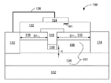
図1は種々の実施形態による集積回路(IC)デバイス100の概略横断面図である。ICデバイス100は基板102上に形成されてもよい。基板102は一般に、その上に層スタック(あるいは単に「スタック101」)が堆積される支持材を含む。ある実施形態では、基板102は、シリコン(Si)、炭化ケイ素(SiC)、酸化アルミニウム(Al2O3)すなわち「サファイア」、窒化ガリウム(GaN)およびまたは窒化アルミニウム(AlN)を含む。他の実施形態では、基板102用として、好適なII〜VI族半導体材料系およびIII〜V族半導体材料系を含む他の材料も使用される。ある実施形態では、その上にバッファ層104の材料がエピタキシャル成長できる任意の材料または材料の任意の組み合わせで基板102を構成してもよい。
FIG. 1 is a schematic cross-sectional view of an integrated circuit (IC)
基板102上に形成されるスタック101は、1つまたは複数のヘテロ接合/ヘテロ構造を形成する異なる材料系で構成されるエピタキシャル堆積層を備えていてもよい。スタック101の層は、その場で(in situ)形成されてもよい。すなわち、スタック101は、基板102を取り出さずにその構成層を形成する(例えばエピタキシャル成長させる)製造装置(例えばチャンバ)内で、基板102上に形成されてもよい。
The
一実施形態では、ICデバイス100のスタック101は、基板102上に形成されたバッファ層104を備える。バッファ層104は、ICデバイス100の基板102と他の構成要素(例えばバリア層106)間に結晶構造転移を与えてもよく、これによって、これら2つの間のバッファ層または絶縁層として作用する。例えば、バッファ層104によって、基板102と他の格子不整合材料(例えばバリア層106)間の応力が緩和され得る。一部の実施形態では、バッファ層104を、トランジスタの可動電荷キャリア用のチャネルとして機能させてもよい。一部の実施形態では、バッファ層104は非ドープであってもよい。バッファ層104を、基板102にエピタキシャルに接続してもよい。他の実施形態では、核形成層(図示せず)を基板102とバッファ層104間に介在させてもよい。一部の実施形態では、バッファ層104を複数の堆積膜あるいは層で構成してもよい。
In one embodiment, the
一部の実施形態では、バッファ層104は、例えば窒化ガリウム(GaN)または窒化アルミニウム(AlN)などのIII族窒化物系材料を含んでいてもよい。バッファ層104の厚みは、その下の基板102の表面に実質的に垂直な方向において1〜2μmであってもよい。他の実施形態では、バッファ層104は、他の好適な材料およびまたは厚みを有していてもよい。
In some embodiments,
スタック101は、バッファ層104上に形成されたバリア層106(「供給層」とも呼ぶ)をさらに備えていてもよい。バリア層106とバッファ層104間には、ヘテロ接合が形成されていてもよい。バリア層106のバンドギャップエネルギーは、バッファ層104のそれより大きくてもよい。バリア層106は、可動電荷キャリアを供給するより広いバンドギャップ層であってもよく、バッファ層104は、該可動電荷キャリア用のチャネルまたは経路を提供するより狭いバンドギャップ層であってもよい。一部の実施形態では、バリア層106のバンドギャップエネルギーは、再成長構造110のバンドギャップエネルギー以下であってもよい。
The
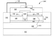
バリア層106は、例えばIII族窒化物系材料などの種々の好適な材料系のうちの任意のもので構成されてもよい。バリア層106は、例えばアルミニウム(Al)、インジウム(In)、ガリウム(Ga)およびまたは窒素(N)を含んでいてもよい。一部の実施形態では、単一材料から成る単独層でバリア層106を構成してもよい。一実施形態では、例えば窒化アルミニウムガリウム(AlxGa1−xN)(x:アルミニウムとガリウムの相対量を表す0〜1の値)の単独層でバリア層106を構成してもよい。他の実施形態では、複数の堆積膜あるいは層でバリア層106を構成してもよい。例えば、図2に示すように、ICデバイス200は、バッファ層104上に配置された第1バリア層107と、第1バリア層107上に配置された第2バリア層108とで構成されるバリア層106を備えていてもよい。一部の実施形態では、窒化アルミニウム(AlN)で第1バリア層107を構成し、窒化インジウムアルミニウム(InAlN)、窒化アルミニウムガリウム(AlGaN)または窒化インジウムガリウムアルミニウム(InGaAlN)で第2バリア層108を構成してもよい。他の実施形態では、バリア層106は、他の材料あるいは図示されたものより多くの層を含んでいてもよい。ICデバイス200は、図1のICデバイス100に関連して説明した実施形態に適合していてもよい。
図1に戻り、バッファ層104とバリア層106間の界面(例えばヘテロ接合)に二次元電子ガス(2DEG)を形成して、ソース端子(以後、ソース112)とドレイン端子(以後、ドレイン114)間に電流(例えば可動電荷キャリア)が流れるようにしてもよい。一部の実施形態では、ICデバイス100は、その中に電流を流すために、電源電圧に対して正のゲート電圧を用いるエンハンスメントモード(Eモード)デバイスであってもよい。こうした実施形態では、再成長構造110とバッファ層104間のバリア層106の厚みTは、2DEG形成のための臨界厚みT0(例えば、臨界厚みT0未満であれば2DEGは生じ得ない)未満であってもよい。例えば、厚みTは、ゲート端子(以後、「ゲート118」)とバッファ層104間に配置されたチャネルのゲート領域では2DEGの形成を阻止し、一方、該ゲート領域とソース112間および該ゲート領域とドレイン114間のチャネルのアクセス領域では2DEGが形成されるように構成されてもよい。一部の実施形態では、バリア層106の厚みおよびまたはアルミニウム含量は、ショットキー(Schottky)ゲートデバイスかMISゲートデバイスのいずれかであるデバイス100に対しては、該ゲート領域における2DEGをすべて確実に除去するように選択されてもよい。他の実施形態では、ICデバイス100は、その中の電流を低減するために、電源電圧に対して負のゲート電圧を用いるデプレションモード(Dモード)デバイスであってもよい。
Returning to FIG. 1, a two-dimensional electron gas (2DEG) is formed at the interface (for example, heterojunction) between the
一部の実施形態では、該ゲート領域におけるバリア層106の厚みTは30Å以下である。例えば、AlGaNの単独層で構成されるバリア層106のゲート領域における厚みTは、20Å以下であってもよい。AlNおよびまたはInAlNで構成されるバリア層106のゲート領域における厚みTは、15Å以下であってもよい。一部の実施形態では、バリア層106の厚みTは10Å〜50Åであってもよい。一部の実施形態では、バリア層106のゲート領域外の領域における厚みは、その下のバッファ層104の表面に実質的に垂直な方向において160Å〜300Åであってもよい。他の実施形態では、バリア層106は、他の好適な材料およびまたは厚みを有していてもよい。
In some embodiments, the thickness T of the
種々の実施形態では、ICデバイス100は、図示のように、バリア層106内に配置された再成長構造110をさらに備える。再成長構造110は、バリア層106の材料が除去され、そこに再成長構造110の材料が堆積または再成長され得ることを示すために「再成長」と呼ばれ得る。一部の実施形態では、再成長構造110をゲート118の絶縁層として機能させて、Eモードデバイスを得てもよい。介在するバリア層106(例えばバリア層106の厚みT)によって、バッファ層104とバリア層106間のチャネル界面を保護し、ゲート凹部/形成プロセスの一部として、チャネル界面を露出する従来の凹部プロセスまたは堆積プロセスに付随するトラップまたは他の欠陥を生じることなく、絶縁層(例えば再成長構造110)が形成できるようにしてもよい。
In various embodiments, the
一部の実施形態では、図示のように、再成長構造110は、バリア層106(例えば、図2の第1バリア層107および第2バリア層108)にエピタキシャルに接続してもよい。図示のように、再成長構造110をゲート118とバッファ層104間に配置してもよい。種々の実施形態では、再成長構造110のバンドギャップエネルギーは、バリア層106およびバッファ層104のそれより大きくてもよい。ある実施形態では、再成長構造110のバンドギャップは5eV以上であってもよい。例えば、再成長構造110のバンドギャップエネルギーは5〜6eVであってもよい。再成長構造110のバンドギャップエネルギーは、バリア層106およびまたはバッファ層104のそれより大きくてもよい。一部の実施形態では、再成長構造110は、ゲート118とバッファ層104間に配置されたゲート領域における2DEGの形成を阻止する動作機能を有していてもよい。再成長構造110は、ICデバイス100のチャネルを塞ぐように構成されて、ゲート領域(例えばチャネル)内の面積抵抗率を上昇させてもよい。例えば、AlGaN層を有するウェーハの面積抵抗率は約500Ω/□であってもよい。低温プロセスを用いて、AlGaN層上に100Å厚のGaN層を堆積後では、面積抵抗率は約1500Ω/□であってもよい。
In some embodiments, as shown, the
再成長構造110は、例えばIII族窒化物系材料などの種々の好適な材料系のうちの任意のもので構成されてもよい。再成長構造110は、例えばアルミニウム(Al)、インジウム(In)、ガリウム(Ga)およびまたは窒素(N)を含んでいてもよい。一部の実施形態では、再成長構造110は、窒素(N)とアルミニウム(Al)またはガリウム(Ga)の内の少なくとも1つとを含んでいてもよい。例えば窒化ガリウム(GaN)、窒化アルミニウム(AlN)、窒化インジウムガリウム(InGaN)、窒化インジウムアルミニウム(InAlN)、窒化アルミニウムガリウム(AlGaN)または窒化インジウムガリウムアルミニウム(InGaAlN)で、再成長構造110を構成してもよい。ある実施形態では、GaNで再成長構造110を構成し、AlGaNまたはAlN/InAlNでバリア層106を構成(例えば、図2の第1バリア層107がAlNであり、第2バリア層108がInAlNである)し、GaNでバッファ層104を構成する。
種々の実施形態では、高温(HT)プロセスまたは低温(LT)プロセスを用いてIII族窒化物を堆積して、再成長構造110を形成してもよい。高温プロセスは、例えば、600℃を超える温度(例えば700℃〜800℃)で、例えばGaNなどのIII族窒化物を堆積して、低温プロセスで製造される構造より結晶性の(例えば、より単結晶に近くより非晶質でない)構造を形成するプロセスを備えていてもよい。低温プロセスは、例えば、600℃以下の温度で、例えばGaNなどのIII族窒化物をエピタキシャルに堆積して、高温プロセスで製造される構造より非晶質なあるいは多結晶の構造を形成するプロセスを備えていてもよい。例えば、一実施形態では、再成長構造110は、350℃〜500℃の温度でのエピタキシャル堆積で堆積されたGaNを含んでいてもよい。高温プロセスでは、材料をより付随的なトラップを形成をし易くする圧電性の再成長構造110の材料が生成され得るため、高温プロセスを用いて材料を堆積して再成長構造110を形成すると、ICデバイス100における電流崩壊とゲートリークが上昇し得る。低温プロセスでの再成長構造110の形成では、より多結晶または非晶質な格子構造を有する材料が得られ、これによって、トラップ形成が低減されて、ICデバイス100における電流崩壊とゲートリークが軽減できる。一部の実施形態では、再成長構造110は、低温プロセスで形成された実質的に多結晶または非晶質の格子構造を含む。
In various embodiments, the III-nitride may be deposited to form the
種々の実施形態では、再成長構造110の厚みは200Å以下であってもよい。再成長構造110の厚みは、バリア層106の下位にあるバッファ層104の表面に実質的に垂直な方向において、例えば25Å〜200Åであってもよい。他の実施形態では、再成長構造110の厚みおよび材料は他のものであってもよい。
In various embodiments, the thickness of
ICデバイス100は、図示のように、バリア層106(例えば、図2の第1バリア層107および第2バリア層108)内に配置されたゲート118をさらに備えていてもよい。ゲート118は、図示のように、チャネル(例えば、ICデバイス100のオン/オフ状態)を制御するように構成されてもよい。ゲート118をICデバイス100の接続端子として機能させてもよく、図示のように、バリア層106および再成長構造110と物理的に直接接触させてもよい。一部の実施形態では、図示のように、ゲート118を、例えば、バリア層106上に形成された窒化ケイ素(SiN)または別の誘電材料などの誘電体層116上に形成してもよい。
The
ゲート118は、図示のように、バリア層106に接続されたトランク部すなわち底部と、該トランク部から、その上にスタック101が形成された基板102の表面に実質的に平行な逆方向に離れるように延在する頂部と、を有していてもよい。ゲート118のトランク部および頂部のこうした構成をT形フィールドプレートゲートと呼んでもよい。すなわち、一部の実施形態では、ゲート118は、ゲート118とドレイン114間の絶縁破壊電圧を上昇させ得およびまたはその電界を低減させ得る一体型フィールドプレート(例えばゲート118の頂部)を有していてもよい。該一体型フィールドプレートによって、ICデバイス100の高電圧動作が容易になり得る。
ゲート118は、ICデバイス100のしきい値電圧に対する電気経路を提供するゲート電極(例えば、図8のゲート電極118a)と、ゲート電極とバリア層106間およびまたはゲート電極と再成長構造110間に配置され得るゲート誘電体すなわちゲート絶縁体(以後、「ゲート絶縁体膜」と呼ぶ、例えば図8のゲート絶縁体膜118b)と、を備えていてもよい。金属などの導電性材料でゲート電極を構成してもよい。一部の実施形態では、ニッケル(Ni)、プラチナ(Pt)、イリジウム(Ir)、モリブデン(Mo)、金(Au)およびまたはアルミニウム(Al)で、ゲート電極を構成してもよい。ある実施形態では、バリア層106とのゲートコンタクトを得るために、Ni、Pt、IrまたはMoを含む材料がゲート118のトランク部内に配置され、ゲート118の導電性と低抵抗を確実にするために、Auを含む材料がゲート118の頂部内に配置される。
種々の実施形態では、ゲート118は、ICデバイス100のショットキー接合か金属−絶縁体−半導体(MIS)接合を提供するように構成されてもよい。例えば、ゲート絶縁体膜がゲート誘電体であるか、あるいは全く使用されない場合には、ショットキー接合が形成されてもよく、ゲート絶縁体膜がゲート絶縁体である場合には、MIS接合が形成されてもよい。一部の実施形態では、ゲート誘電体は、厚みがゲート絶縁体より小さい薄膜であってもよい。ゲート絶縁体膜は、例えば、窒化ケイ素(SiN)、酸化シリコン(SiO2)、酸化アルミニウム(Al2O3)およびまたは酸化ハフニウム(HfO2)を含んでいてもよい。他の実施形態では、ゲート絶縁体膜は他の材料を含んでいてもよい。
In various embodiments,
ICデバイス100は、バリア層106上に形成されたソース112とドレイン114を備えていてもよい。ソース112とドレイン114は、図示のように、バリア層106を通ってバッファ層104内に延在していてもよい。種々の実施形態では、ソース112とドレイン114はオーミックコンタクトである。ソース112とドレイン114は、標準の成長コンタクトよりコンタクト抵抗が比較的小さいものであり得る再成長コンタクトであってもよい。
The
金属などの導電性材料で、ソース112とドレイン114を構成してもよい。ある実施形態では、ソース112とドレイン114は、チタン(Ti)、アルミニウム(Al)、モリブデン(Mo)、金(Au)およびまたはシリコン(Si)を含んでいてもよい。他の実施形態では、他の材料が用いられる。
The
ある実施形態では、ドレイン114とゲート118間の距離D1は、ソース112とゲート118間の距離S1より大きい。一部の実施形態では、距離D1は、ドレイン114とゲート118間の最短距離であってもよく、距離S1は、ソース112とゲート118間の最短距離であってもよい。距離S1を距離D1より短くすることによって、ゲート118−ドレイン114間の絶縁破壊電圧を上昇させ得、およびまたはソース112の抵抗を低減させ得る。
In some embodiments, the
一部の実施形態では、図示のように、誘電体層122をゲート118およびまたは誘電体層116上に形成してもよい。誘電体層122は、例えば窒化ケイ素(SiN)を含んでいてもよい。他の実施形態では、誘電体層122には他の材料が用いられる。誘電体層122は、ゲート118の頂部を実質的に封入してもよい。一部の実施形態では、誘電体層122をデバイス100の保護層として機能させてもよい。
In some embodiments,
ICデバイス100は、ゲート118とドレイン114間の絶縁破壊電圧を上昇させおよびまたは電界を低減するために、誘電体層122上に形成されたフィールドプレート124をさらに備えていてもよい。導電性材料126を用いて、フィールドプレート124をソース112に電気的に接続してもよい。導電性材料126は、誘電体層122上に電極あるいはトレース状の構造物として堆積された、例えば金(Au)などの金属を含んでいてもよい。他の実施形態では、導電性材料126に他の好適な材料を使用してもよい。
The
フィールドプレート124は、金属などの導電性材料で構成され、ゲート118に関連して説明した材料を含んでいてもよい。フィールドプレート124は、誘電体層122を通してゲート118に容量接続されてもよい。一部の実施形態では、フィールドプレート124とゲート118間の最短距離は1000Å〜2000Åである。フィールドプレート124は、オーバーハング領域が得られるように、図示のように、その一部分がゲート118の上部に直接形成されないようにしてゲート118の上部に形成されてもよい。一部の実施形態では、フィールドプレート124のオーバーハング領域は、ゲート118の頂部端部より距離H1だけ延在する。一部の実施形態では、距離H1は0.2〜1μであってもよい。他の実施形態では、H1は他の値であってもよい。
種々の実施形態では、ICデバイス100は高電子移動度トランジスタ(HEMT)であってもよい。一部の実施形態では、ICデバイス100はショットキーデバイスであってもよい。他の実施形態では、MIS電界効果トランジスタ(MISFET)であってもよい。一部の実施形態では、ゲート118は、例えば、Eモードスイッチデバイスのスイッチングを制御するように構成されてもよい。ICデバイス100は、無線周波数(RF)用途、ロジック用途およびまたは電力変換用途に使用されてもよい。例えば、ICデバイス100によって、例えば交流(AC)−直流(DC)変換器、DC−DC変換器、DC−AC変換器などの電力調整用途を含む電力スイッチ用途用の効果的なスイッチデバイスが提供され得る。
In various embodiments,
図3〜8は、種々の製造作業後のデバイス(例えば図2のデバイス200)を示す。図3〜8に関連して説明する方法と構成は、図1〜2に関連して説明した実施形態に適合し得、逆もまたそうである。
3-8 illustrate the device (e.g.,
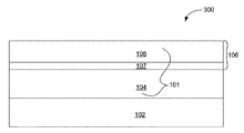
図3は、種々の実施形態による、基板102上への層スタック(例えばスタック101)形成後のICデバイス300の概略横断面図である。種々の実施形態では、ICデバイス300は、基板102上にバッファ層104を堆積し、バッファ層104上にバリア層106を堆積して作られてもよい。バリア層106は、バッファ層104上に堆積された第1バリア層107と、第1バリア層107上に堆積された第2バリア層108とを備えていてもよい。一部の実施形態では、例えば分子線エピタキシャル法(MBE)、原子層エピタキシャル法(ALE)、化学ビームエピタキシャル法(CBE)およびまたは有機金属化学気相蒸着法(MOCVD)などのエピタキシャル堆積プロセスを用いて、スタック101の層を堆積してもよい。他の実施形態では、他の堆積プロセスを用いてもよい。
FIG. 3 is a schematic cross-sectional view of an
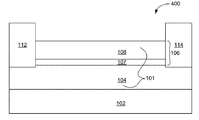
図4は、種々の実施形態による、ソース112とドレイン114形成後のICデバイス400の概略横断面図である。種々の実施形態では、バリア層106上に(例えば、第2バリア層108上に)、ソース112とドレイン114を形成してもよい。ある実施形態では、ソース112とドレイン114が形成される領域内のバリア層106上に、例えば蒸発プロセスを用いて、1つまたは複数の金属などの材料が堆積される。ソース112とドレイン114形成のための材料は、下記の順序で堆積される金属が含まれ得る。チタン(Ti)、その後アルミニウム(Al)、その後モリブデン(Mo)、その後チタン(Ti)、その後金(Au)。該堆積材料を加熱(例えば、高速熱アニールプロセスを用いて約850℃×で約30秒間)して、この材料を貫通させて、下部のバリア層106(例えば第1バリア層107および第2バリア層108)およびまたはバッファ層104と溶融させてもよい。実施形態では、ソース112とドレイン114はそれぞれ、バリア層106を経由してバッファ層104内に延在する。ソース112およびドレイン114の厚みは1000Å〜2000Åであってもよい。他の実施形態では、ソース112とドレイン114の厚みはこれ以外であってもよい。
FIG. 4 is a schematic cross-sectional view of
ソース112とドレイン114を再成長プロセスで形成し、低減された接触抵抗または低減されたオン抵抗を有するオーミックコンタクトを得てもよい。該再成長プロセスでは、ソース112とドレイン114が形成される領域において、バリア層106およびまたはバッファ層104の材料を選択的に除去(例えば、エッチング)してもよい。これらの層が選択的に除去された領域に、高濃度ドープ材料(例えばn++材料)を堆積してもよい。ソース112とドレイン114の高濃度ドープ材料は、バッファ層104またはバリア層106に使用した材料と同様の材料であってもよい。例えば、バッファ層がGaNを含むシステムでは、前記選択的に除去した領域に、シリコン(Si)で高濃度にドープされたGaN系材料を厚みが400Å〜700Åになるまでエピタキシャルに堆積してもよい。分子線エピタキシャル法(MBE)、原子層エピタキシャル法(ALE)、化学ビームエピタキシャル法(CBE)、有機金属化学気相蒸着法(MOCVD)またはこれらの好適な組み合わせによって、前記高濃度ドープ材料をエピタキシャルに堆積できる。他の実施形態では、前記高濃度ドープ材料に対して、他の材料、厚みあるいは堆積法が用いられる。例えばチタン(Ti)およびまたは金(Au)を含む1つまたは複数の金属を、例えばリフトオフプロセスを用いて1000Å〜1500Åの厚みで、該高濃度ドープ材料上に形成/堆積できる。他の実施形態では、該1つまたは複数の金属に対して、他の材料、厚みおよびまたは方法が用いられる。
The
一部の実施形態では、不純物(例えばシリコン)を導入してソース112とドレイン114に高濃度ドープ材料を提供する注入法を用いた注入プロセスによって、ソース112とドレイン114を形成してもよい。注入後、ソース112とドレイン114を高温(例えば1100℃〜1200℃)でアニールしてもよい。前記再成長プロセスでは、前記注入後アニールに伴う高温を好適に避け得る。
In some embodiments,
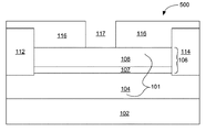
図5は、種々の実施形態による、誘電体層116の堆積およびパターン化後の集積回路(IC)デバイス500の概略横断面図である。一部の実施形態では、バリア層106上に誘電材料を堆積することにより、誘電体層116を形成してもよい。誘電体層116は例えば、窒化ケイ素(SiN)あるいは他の適切な誘電材料を含むことができ、例えば化学気相蒸着法(CVD)、物理的気相蒸着法(PVD)および(または)原子層蒸着法(ALD)などの任意の適切な堆積プロセスを用いて堆積されてもよい。例えばリソグラフィおよびまたはエッチングプロセスなどの任意の適切なプロセスを用いて誘電体層116をパターン化して、誘電体層116にゲート凹部開口部117を形成してもよい。
FIG. 5 is a schematic cross-sectional view of an integrated circuit (IC)
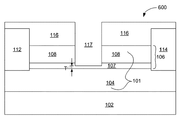
図6は、種々の実施形態による、バリア層106材料除去後の集積回路(IC)デバイス600の概略横断面図である。種々の実施形態では、バリア層106の材料を除去して、図示のように、ゲート凹部開口部117を形成してもよい。バリア層106に再成長構造(例えば図7の再成長構造110)がその後形成できるように、また、バリア層106にゲート(例えば図8のゲート絶縁体膜118bおよびゲート電極118a)が形成できるように、ゲート凹部開口部117を形成してもよい。
FIG. 6 is a schematic cross-sectional view of an integrated circuit (IC)
例えば、ドライ/プラズマまたはウェットエッチングプロセス(例えば時限または選択的エッチングプロセス)を含む任意の適切なプロセスを用いて、バリア層106の材料を除去してもよい。一部の実施形態では、誘電体層116は、バリア層106の材料を除去するエッチングプロセスの間、ハードマスクとして機能し得る。
The material of
一部の実施形態では、バリア層106の材料を除去して、図1に関連して説明した、例えば時限エッチングや選択的エッチングなどによって制御され得る厚みTを得てもよい。ある実施形態では、ゲート凹部開口部117の下部境界が第1バリア層107内に配置されるように、第2バリア層108の材料を除去する。すなわち、ゲート凹部開口部117は、第2バリア層108を完全に貫通してもよい。一部の実施形態では、第1バリア層107の材料を図示のように除去してもよい。一部の実施形態では、バッファ層104の材料がゲート凹部開口部117に露出しないように、第1バリア層107の材料を除去してもよい。他の実施形態では、ゲート凹部開口部117の下部境界は、第1バリア層107内には延在(例えば5Åを超えて)せずに、その上部境界に配置されていてもよい。他の実施形態では、ゲート凹部開口部117の下部境界は、第2バリア層108内に配置されていてもよい(例えば、ゲート凹部開口部117によって、第1バリア層107の材料を露出しない)。
In some embodiments, the material of
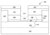
図7は、種々の実施形態による、再成長構造110形成後の集積回路(IC)デバイス700の概略横断面図である。III族窒化物をゲート凹部開口部(例えば、図6のゲート凹部開口部117)内にエピタキシャルに堆積することによって、再成長構造110を形成してもよい。例えば、分子線エピタキシャル法(MBE)、原子層エピタキシャル法(ALE)、化学ビームエピタキシャル法(CBE)、有機金属化学気相蒸着法(MOCVD)またはこれらの好適な組み合わせによって、再成長構造110を堆積してもよい。種々の実施形態では、図1に関連して説明した低温(LT)プロセスを用いて、該堆積プロセスを行ってもよい。例えば、一実施形態では、再成長構造110は、350℃〜500℃の温度でのエピタキシャル堆積によって堆積されたGaNを含んでいてもよい。種々の実施形態では、再成長構造110の厚みは200Å以下であってもよい。再成長構造110の厚みは、バリア層106の下位にあるバッファ層104の表面に実質的に垂直な方向において、例えば25Å〜200Åであってもよい。他の実施形態では、再成長構造110の厚みおよび材料は他のものであってもよい。
FIG. 7 is a schematic cross-sectional view of an integrated circuit (IC)
一部の実施形態では、再成長構造110形成のために堆積される材料を、再成長構造110形成のために用いられる堆積プロセスの間に、誘電体層116上にキャッピング層610として堆積してもよい。一部の実施形態では、顧客に出荷されるICデバイスの最終製品中に誘電体層116およびまたはキャッピング層610が存在し得ないように、ゲート形成前に、それらの内のいずれかまたは両方を除去してもよい。
In some embodiments, the material deposited for
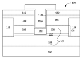
図8は、種々の実施形態による、ゲート(例えば図1のゲート118)形成後の集積回路(IC)デバイス800の概略横断面図である。該ゲートは、ゲート電極118aと、一部の実施形態では、ゲート絶縁体膜118bと、を備えていてもよい。
FIG. 8 is a schematic cross-sectional view of an integrated circuit (IC)
一部の実施形態では、誘電材料または電気絶縁材料を堆積してゲート絶縁体膜118bを形成してもよい。ゲート誘電体膜118bの材料は、例えば、窒化ケイ素(SiN)、酸化シリコン(SiO2)、酸化アルミニウム(Al2O3)およびまたは酸化ハフニウム(HfO2)で構成されていてもよい。他の実施形態では、他の方法または材料を用いてゲート誘電体膜118bを形成してもよい。一部の実施形態では、ゲート誘電体膜118を全く使用しなくてもよい。
In some embodiments, a dielectric or electrically insulating material may be deposited to form the
ゲート凹部開口部(例えば図6のゲート凹部開口部117)内に導電性材料を堆積することによって、ゲート電極118aを形成してもよい。ゲート絶縁体膜118bを用いる実施形態では、その上にゲート電極118aを堆積してもよい。ゲート絶縁体膜118bを用いない実施形態では、図示のように、再成長構造110およびバリア層106の表面上にゲート電極118aを堆積してもよい。例えば蒸発、原子層蒸着法(ALD)およびまたは化学気相蒸着法(CVD)を含む任意の好適な堆積プロセスによって、該導電性材料を堆積してもよい。
The
図9は、種々の実施形態による、集積回路デバイス(例えば、図1〜2のICデバイス100または200)の製造方法900を示すフロー図である。該方法は、図1〜8に関連して説明した方法と構成に適合していてもよい。
FIG. 9 is a flow diagram illustrating a
方法900は、902において、基板(例えば、図1の基板102)上にバッファ層(例えば、図1のバッファ層104)を形成するステップを備える。バッファ層を形成するステップは、基板上にバッファ層材料をエピタキシャルに堆積するステップを備えていてもよい。一部の実施形態では、該バッファ層を複数の層で構成してもよい。
The
方法900は、904において、バッファ層(例えば、図1のバッファ層104)上にバリア層(例えば、図1のバリア層106)を形成するステップをさらに備えていてもよい。バリア層を形成するステップは、バッファ層上にバリア層材料をエピタキシャルに堆積するステップを備えていてもよい。一部の実施形態では、バリア層を複数の層(例えば、図2の第1バリア層107および第2バリア層108)で構成してもよい。他の実施形態では、単独層の材料を堆積してバリア層を形成してもよい。
The
方法900は、906において、ソース(例えば、図1のソース112)とドレイン(例えば、図1のドレイン114)とを形成するステップをさらに備えていてもよい。一部の実施形態では、ソースとドレインはバリア層に接続され、バリア層を通ってバッファ層内に延在していてもよい。
The
方法900は、908において、バリア層内に再成長構造(例えば、図1の再成長構造110)を形成するステップをさらに備えていてもよい。一部の実施形態では、再成長構造を形成するステップは、バリア層の材料を除去してその中に開口部(例えば、図6のゲート凹部開口部117)を形成するステップと、該開口部内に再成長構造材料を堆積するステップとを備えていてもよい。一部の実施形態では、エピタキシャル堆積プロセスで該再成長構造を堆積してもよい。一部の実施形態では、再成長構造材料を堆積するステップは、再成長構造材料を200Å以下の厚みで堆積するステップを備える。
The
方法900は、910において、バリア層内にゲート端子(例えば、図1のゲート118)を形成するステップをさらに備えていてもよい。一部の実施形態では、ゲート端子を形成するステップは、バリア層の開口部内の再成長構造上にゲート絶縁体膜(例えば図8のゲート絶縁体膜118b)を堆積するステップを備える。一部の実施形態では、ゲート端子を形成するステップは、ゲート絶縁体膜上にゲート電極材料を堆積するステップ、あるいはゲート絶縁体膜を堆積しない実施形態では、バリア層の開口部内の再成長構造上にゲート電極材を堆積するステップを備える。ゲート電極をバリア層の材料に接続してショットキー接合またはMIS接合を形成してもよい。種々の実施形態では、バリア層の材料を除去してその中に開口部を形成するステップは、908におけるバリア層内に再成長構造を形成するステップの一部であってもよく、また、910におけるバリア層内にゲート端子を形成するステップの一部であってもよい。エッチングプロセスでバリア層の材料を除去して開口部を形成してもよい。
The
方法900は、912において、ゲート上に誘電体層(例えば、図1の誘電体層116およびまたは122)を形成するステップをさらに備えていてもよい。任意の好適な堆積プロセスによって誘電体層を堆積してもよい。種々の実施形態では、誘電体層は、ICデバイスの保護層として機能し得る。
方法900は、914において、誘電体層上にフィールドプレートを形成するステップをさらに備えていてもよい。任意の好適な堆積法を用いて導電性材料を前記誘電体層上に堆積することにより、フィールドプレートを形成してもよい。リソグラフィプロセスおよびまたはエッチングプロセスなどのパターン化プロセスを用いて前記堆積した導電性材料部分を選択的に除去して、フィールドプレートを形成できる。他の実施形態では、他の好適な方法を用いてもよい。
The
特許請求された主題の理解に最も有用な順番と方法で、種々の操作が複数の別個の操作として説明される。しかしながら、説明の順番は、これらの操作が必ず順番依存であることを示唆するように解釈されるべきでない。これらの操作は、特に提示の順番に行われなくてもよい。記載の実施形態と異なる順番で、記載された操作を行ってもよい。追加の実施形態では、種々の追加の操作を行ってもよく、およびまたは記載の操作を省略してもよい。 The various operations are described as a plurality of separate operations in the order and manner most useful for understanding the claimed subject matter. However, the order of description should not be construed to imply that these operations are necessarily order dependent. These operations do not have to be performed particularly in the order of presentation. The described operations may be performed in a different order than the described embodiments. In additional embodiments, various additional operations may be performed and / or described operations may be omitted.
本明細書に記載のICデバイス(例えば、図1、2および8のICデバイス100、200および800)の実施形態およびこうしたICデバイスを備える装置を、他の種々の装置およびシステムに組み込んでもよい。システム例1000のブロック図を図10に示す。図示のように、システム1000は、一部の実施形態では、無線周波数(RF)電力増幅器(PA)モジュールであり得るPAモジュール1002を備える。システム1000は、図示のように、電力増幅器モジュール1002に接続されたトランシーバ1004を備えていてもよい。電力増幅器モジュール1002は、本明細書に記載のICデバイス(例えば、図1、2および8のICデバイス100、200および800)を備えていてもよい。
Embodiments of the IC devices described herein (eg,
電力増幅器モジュール1002は、トランシーバ1004からRF入力信号(RFin)を受信してもよい。電力増幅器モジュール1002は、該RF入力信号(RFin)を増幅してRF出力信号(RFout)を出力してもよい。RF入力信号(RFin)およびRF出力信号(RFout)は、それぞれ図10のTx−RFinおよびTx−RFoutで示され、共に送信チェーンの一部であり得る。
The power amplifier module 1002 may receive an RF input signal (RFin) from the
増幅されたRF出力信号(RFout)は、アンテナスイッチモジュール(ASM)1006に与えられてもよく、このモジュールによって、アンテナ構造1008経由で、RF出力信号(RFout)の無線(OTA)送信が実現される。また、ASM1006は、アンテナ構造1008経由でRF信号を受信し、その受信RF信号(Rx)を受信チェーンに沿ってトランシーバ1004に接続し得る。
The amplified RF output signal (RFout) may be provided to an antenna switch module (ASM) 1006, which implements over-the-air (OTA) transmission of the RF output signal (RFout) via the
種々の実施形態では、アンテナ構造1008は、例えば、ダイポールアンテナ、モノポールアンテナ、パッチアンテナ、ループアンテナ、マイクロストリップアンテナ、あるいはRF信号のOTA送信/受信に好適な任意の他の形式のアンテナを含む指向性アンテナおよびまたは全方向性アンテナの1つまたは複数を備えていてもよい。
In various embodiments,
システム1000は、電力増幅を含む任意のシステムであってもよい。前記ICデバイス(例えば、図1、2および8のICデバイス100、200および800)によって、例えば交流(AC)−直流(DC)変換器、DC−DC変換器、DC−AC変換器などの電力調整用途を含む電力スイッチ用途用の効果的なスイッチデバイスが提供され得る。種々の実施形態では、システム1000は、高無線周波数電力と周波数における電力増幅には特に有用であり得る。システム1000は、例えば、陸上および衛星通信、レーダーシステム、および恐らく種々の産業および医学用途におけるいずれか1つまたは複数に対して好適であり得る。より具体的には、種々の実施形態において、システム1000は、レーダー装置、衛星通信装置、携帯電話、携帯電話基地局、ラジオ放送あるいはテレビ増幅器システムから選択された1つであり得る。
説明の目的で実施形態を例示し記載したが、同じ目的を実現するように意図された、広範な代替となるおよびまたは均等な実施形態あるいは実施によって、本開示の範囲を逸脱することなくこれらの実施形態を置換できる。本出願は、本明細書で検討した実施形態に対するいかなる適応や変形もカバーするように意図される。従って、本明細書に記載された実施形態は、請求項とその均等物によってのみ限定されることは明らかである。 While the embodiments have been illustrated and described for purposes of illustration, it is intended that the broad alternative and / or equivalent embodiments or implementations intended to accomplish the same purpose should be employed without departing from the scope of the present disclosure. Embodiments can be substituted. This application is intended to cover any adaptations or variations to the embodiments discussed herein. Therefore, it is manifest that the embodiments described herein are limited only by the claims and their equivalents.
Claims (26)
前記バッファ層上に配置され、窒化アルミニウムガリウム(AlGaN)の単独層で構成されるバリア層と、
前記バリア層内に配置されて前記バリア層にエピタキシャルに接続され、窒素(N)とアルミニウム(Al)とを含み、600℃以下の温度でエピタキシャルに堆積された抵抗性再成長構造と、
前記バリア層内に配置されたゲート端子と、を備え、
前記抵抗性再成長構造は、前記ゲート端子と前記バッファ層間に配置され、前記バッファ層と前記ゲート端子間に絶縁層を提供することを特徴とする装置。 A buffer layer disposed on the substrate and comprising gallium (Ga) and nitrogen (N);
A barrier layer disposed on the buffer layer and composed of a single layer of aluminum gallium nitride (AlGaN);
A resistive regrowth structure disposed within the barrier layer and epitaxially connected to the barrier layer, the resistive regrowth structure comprising nitrogen (N) and aluminum (Al) and being epitaxially deposited at a temperature of 600 ° C. or less;
A gate terminal disposed in the barrier layer,
The device is characterized in that the resistive regrowth structure is disposed between the gate terminal and the buffer layer, and provides an insulating layer between the buffer layer and the gate terminal.
前記バリア層は、前記第1のバンドギャップエネルギーより小さい第2のバンドギャップエネルギーを有しており、
前記バッファ層は、前記第2のバンドギャップエネルギーより小さい第3のバンドギャップエネルギーを有していることを特徴とする請求項5に記載の装置。 The band gap energy of the resistive regrowth structure is a first band gap energy,
The barrier layer has a second band gap energy smaller than the first band gap energy;
The device of claim 5, wherein the buffer layer has a third band gap energy less than the second band gap energy.
前記ゲート端子は、エンハンスメントモード(Eモード)高電子移動度トランジスタ(HEMT)デバイスのスイッチングを制御するように構成されていることを特徴とする請求項1に記載の装置。 The resistive regrowth structure has an operational function of blocking formation of a two-dimensional electron gas (2DEG) in a gate region disposed between the gate terminal and the buffer layer,
The apparatus of claim 1, wherein the gate terminal is configured to control switching of an enhancement mode (E mode) high electron mobility transistor (HEMT) device.
前記バリア層に接続されたゲート絶縁体膜と、
前記ゲート絶縁体膜に接続され、前記バリア層の材料に接続されてショットキー接合または金属−絶縁体−半導体(MIS)接合を形成するゲート電極と、を備えることを特徴とする請求項1に記載の装置。 The gate terminal is
A gate insulator film connected to the barrier layer;
A gate electrode connected to the gate insulator film and connected to a material of the barrier layer to form a Schottky junction or a metal-insulator-semiconductor (MIS) junction. The device described.
前記バリア層に接続されたドレインと、をさらに備え、前記ソースと前記ドレインは、前記バリア層を通って前記バッファ層内に延在することを特徴とする請求項1に記載の装置。 A source connected to the barrier layer;
The device of claim 1, further comprising: a drain connected to the barrier layer, wherein the source and the drain extend through the barrier layer into the buffer layer.
前記ゲート端子は、ニッケル(Ni)、白金(Pt)、イリジウム(Ir)、モリブデン(Mo)または金(Au)を含むことを特徴とする請求項11に記載の装置。 The gate terminal is a T-shaped field plate gate;
The device of claim 11, wherein the gate terminal comprises nickel (Ni), platinum (Pt), iridium (Ir), molybdenum (Mo) or gold (Au).
アルミニウム(Al)と窒素(N)とを含むバリア層を前記バッファ層上に形成するステップと、
前記バリア層の材料を除去してその中に開口部を形成し、600℃以下の温度で、窒素(N)とアルミニウム(Al)とを含む抵抗性再成長構造を前記バリア層の開口部内に堆積することによって、前記バリア層内に抵抗性再成長構造を形成するステップと、を備えることを特徴とする方法。 Forming a buffer layer comprising gallium (Ga) and nitrogen (N) on a substrate;
Forming a barrier layer comprising aluminum (Al) and nitrogen (N) on the buffer layer;
The material of the barrier layer is removed to form an opening therein, and a resistive regrowth structure including nitrogen (N) and aluminum (Al) is formed in the opening of the barrier layer at a temperature of 600 ° C. or less Forming a resistive regrowth structure in the barrier layer by depositing.
前記バリア層を形成するステップは、前記バッファ層上にバリア層材料をエピタキシャルに堆積するステップを備え、
前記抵抗性再成長構造の材料を堆積するステップは、前記バリア層の開口部内に前記抵抗性再成長構造の材料をエピタキシャルに堆積するステップを備えることを特徴とする請求項15に記載の方法。 Forming the buffer layer comprises epitaxially depositing a buffer layer material on the substrate;
Forming the barrier layer comprises epitaxially depositing a barrier layer material on the buffer layer;
16. The method of claim 15, wherein depositing a material of the resistive regrowth structure comprises epitaxially depositing a material of the resistive regrowth structure in the opening of the barrier layer.
前記第1の層は、前記バッファ層にエピタキシャルに接続され、また、窒化アルミニウム(AlN)を含んでおり、
前記第2の層は、前記第1の層にエピタキシャルに接続され、また、窒化インジウムアルミニウム(InAlN)、窒化アルミニウムガリウム(AlGaN)または窒化インジウムガリウムアルミニウム(InGaAlN)を含んでおり、
前記抵抗性再成長構造は、前記第1の層と前記第2の層とに物理的に直接接触していることを特徴とする請求項16に記載の方法。 Forming the barrier layer comprises forming a plurality of layers including a first layer and a second layer;
The first layer is epitaxially connected to the buffer layer and includes aluminum nitride (AlN);
The second layer is epitaxially connected to the first layer and includes indium aluminum nitride (InAlN), aluminum gallium nitride (AlGaN) or indium gallium aluminum nitride (InGaAlN).
17. The method of claim 16, wherein the resistive regrowth structure is in direct physical contact with the first layer and the second layer.
前記バリア層の材料を除去してバリア層内に開口部を形成するステップをさらに備え、
前記バリア層の材料を除去するステップは、エッチングプロセスで行われることを特徴とする請求項22に記載の方法。 Forming the gate terminal in the barrier layer comprises:
Removing the material of the barrier layer to form an opening in the barrier layer;
The method of claim 22, wherein removing the material of the barrier layer is performed by an etching process.
前記ゲート端子は、エンハンスメントモード(Eモード)高電子移動度トランジスタ(HEMT)デバイスのスイッチングを制御するように構成されていることを特徴とする請求項22に記載の方法。 The resistive regrowth structure has an operational function of blocking formation of a two-dimensional electron gas (2DEG) in a gate region disposed between the gate terminal and the buffer layer,
23. The method of claim 22, wherein the gate terminal is configured to control switching of an enhancement mode (E mode) high electron mobility transistor (HEMT) device.
Applications Claiming Priority (2)
| Application Number | Priority Date | Filing Date | Title |
|---|---|---|---|
| US13/535,127 | 2012-06-27 | ||
| US13/535,127 US8975664B2 (en) | 2012-06-27 | 2012-06-27 | Group III-nitride transistor using a regrown structure |
Related Parent Applications (1)
| Application Number | Title | Priority Date | Filing Date |
|---|---|---|---|
| JP2013132779A Division JP6335444B2 (en) | 2012-06-27 | 2013-06-25 | III-nitride transistor using regrowth structure |
Publications (2)
| Publication Number | Publication Date |
|---|---|
| JP2018082192A JP2018082192A (en) | 2018-05-24 |
| JP6554530B2 true JP6554530B2 (en) | 2019-07-31 |
Family
ID=49754231
Family Applications (2)
| Application Number | Title | Priority Date | Filing Date |
|---|---|---|---|
| JP2013132779A Expired - Fee Related JP6335444B2 (en) | 2012-06-27 | 2013-06-25 | III-nitride transistor using regrowth structure |
| JP2017243108A Expired - Fee Related JP6554530B2 (en) | 2012-06-27 | 2017-12-19 | Group III nitride transistor using regrowth structure |
Family Applications Before (1)
| Application Number | Title | Priority Date | Filing Date |
|---|---|---|---|
| JP2013132779A Expired - Fee Related JP6335444B2 (en) | 2012-06-27 | 2013-06-25 | III-nitride transistor using regrowth structure |
Country Status (4)
| Country | Link |
|---|---|
| US (1) | US8975664B2 (en) |
| JP (2) | JP6335444B2 (en) |
| DE (1) | DE102013010487A1 (en) |
| TW (1) | TWI610438B (en) |
Families Citing this family (47)
| Publication number | Priority date | Publication date | Assignee | Title |
|---|---|---|---|---|
| JP2924064B2 (en) | 1990-03-31 | 1999-07-26 | スズキ株式会社 | Power train |
| US7501669B2 (en) | 2003-09-09 | 2009-03-10 | Cree, Inc. | Wide bandgap transistor devices with field plates |
| US9773877B2 (en) | 2004-05-13 | 2017-09-26 | Cree, Inc. | Wide bandgap field effect transistors with source connected field plates |
| US11791385B2 (en) | 2005-03-11 | 2023-10-17 | Wolfspeed, Inc. | Wide bandgap transistors with gate-source field plates |
| JP5966301B2 (en) | 2011-09-29 | 2016-08-10 | 富士通株式会社 | Compound semiconductor device and manufacturing method thereof |
| US9123533B2 (en) | 2012-08-10 | 2015-09-01 | Avogy, Inc. | Method and system for in-situ etch and regrowth in gallium nitride based devices |
| US8884334B2 (en) * | 2012-11-09 | 2014-11-11 | Taiwan Semiconductor Manufacturing Co., Ltd. | Composite layer stacking for enhancement mode transistor |
| US9171946B2 (en) * | 2013-03-05 | 2015-10-27 | Seoul Semiconductor Co., Ltd. | Nitride semiconductor device and method of manufacturing the same |
| US9679981B2 (en) * | 2013-06-09 | 2017-06-13 | Cree, Inc. | Cascode structures for GaN HEMTs |
| US9755059B2 (en) | 2013-06-09 | 2017-09-05 | Cree, Inc. | Cascode structures with GaN cap layers |
| US9847411B2 (en) * | 2013-06-09 | 2017-12-19 | Cree, Inc. | Recessed field plate transistor structures |
| JP6212124B2 (en) * | 2013-08-30 | 2017-10-11 | 国立研究開発法人科学技術振興機構 | InGaAlN semiconductor device |
| KR102423219B1 (en) * | 2014-12-18 | 2022-07-20 | 인텔 코포레이션 | N-channel gallium nitride transistors |
| TWI569439B (en) * | 2015-03-31 | 2017-02-01 | 晶元光電股份有限公司 | Semiconductor cell |
| CN106298903A (en) * | 2015-05-18 | 2017-01-04 | 中国科学院苏州纳米技术与纳米仿生研究所 | Secondary epitaxy p-type III group-III nitride realizes method and enhancement mode HEMT of enhancement mode HEMT |
| TWI563654B (en) * | 2015-08-26 | 2016-12-21 | Globalwafers Co Ltd | Enhancement-Mode High-Electron-Mobility Transistor Structure |
| JP6746887B2 (en) * | 2015-09-16 | 2020-08-26 | 住友電気工業株式会社 | High electron mobility transistor and method of manufacturing high electron mobility transistor |
| CN105355555A (en) * | 2015-10-28 | 2016-02-24 | 中国科学院微电子研究所 | GaN-based enhanced power electronic device and preparation method thereof |
| US10068976B2 (en) * | 2016-07-21 | 2018-09-04 | Taiwan Semiconductor Manufacturing Co., Ltd. | Enhancement mode field-effect transistor with a gate dielectric layer recessed on a composite barrier layer for high static performance |
| CN106876443A (en) * | 2017-03-03 | 2017-06-20 | 上海新傲科技股份有限公司 | GaN high electron mobility transistor of high-breakdown-voltage and forming method thereof |
| TWI661555B (en) * | 2017-12-28 | 2019-06-01 | Nuvoton Technology Corporation | Enhancement mode hemt device |
| TWI726282B (en) * | 2019-02-19 | 2021-05-01 | 世界先進積體電路股份有限公司 | Semiconductor devices and methods for fabricating the same |
| CN111668302B (en) * | 2019-03-08 | 2023-03-14 | 世界先进积体电路股份有限公司 | Semiconductor device and method for manufacturing the same |
| US11335797B2 (en) | 2019-04-17 | 2022-05-17 | Vanguard International Semiconductor Corporation | Semiconductor devices and methods for fabricating the same |
| CN110676316B (en) * | 2019-09-20 | 2023-04-11 | 中国电子科技集团公司第十三研究所 | Enhancement mode field effect transistor |
| US11658233B2 (en) | 2019-11-19 | 2023-05-23 | Wolfspeed, Inc. | Semiconductors with improved thermal budget and process of making semiconductors with improved thermal budget |
| JP7262379B2 (en) * | 2019-12-16 | 2023-04-21 | 株式会社東芝 | semiconductor equipment |
| CN111463259B (en) * | 2020-03-10 | 2022-09-13 | 安徽长飞先进半导体有限公司 | High electron mobility field effect transistor and preparation method thereof |
| CN111668101B (en) * | 2020-06-03 | 2022-07-01 | 西安电子科技大学 | Enhanced gallium nitride high electron mobility transistor and preparation method thereof |
| JP7325631B2 (en) * | 2020-06-04 | 2023-08-14 | 三菱電機株式会社 | semiconductor equipment |
| WO2022041157A1 (en) * | 2020-08-28 | 2022-03-03 | 华为技术有限公司 | Substrate and power amplification device |
| US11749726B2 (en) | 2020-10-27 | 2023-09-05 | Wolfspeed, Inc. | Field effect transistor with source-connected field plate |
| US11658234B2 (en) * | 2020-10-27 | 2023-05-23 | Wolfspeed, Inc. | Field effect transistor with enhanced reliability |
| US12408403B2 (en) | 2020-10-27 | 2025-09-02 | Macom Technology Solutions Holdings, Inc. | Field effect transistor with stacked unit subcell structure |
| US12266721B2 (en) | 2020-10-27 | 2025-04-01 | Wolfspeed, Inc. | Field effect transistor with multiple stepped field plate |
| US11502178B2 (en) | 2020-10-27 | 2022-11-15 | Wolfspeed, Inc. | Field effect transistor with at least partially recessed field plate |
| WO2022124868A1 (en) * | 2020-12-11 | 2022-06-16 | 경북대학교 산학협력단 | High electron mobility transistor and method for manufacturing same |
| US12261168B2 (en) | 2021-02-16 | 2025-03-25 | Efficient Power Conversion Corporation | Gate metal-insulator-field plate metal integrated circuit capacitor and method of forming the same |
| CN113113478B (en) * | 2021-03-01 | 2022-10-04 | 西安电子科技大学 | GaN-based radio frequency power device based on ohmic regrowth and preparation method thereof |
| US11581448B2 (en) * | 2021-04-01 | 2023-02-14 | Raytheon Company | Photoconductive semiconductor switch laterally fabricated alongside GaN on Si field effect transistors |
| US12199174B2 (en) * | 2021-06-25 | 2025-01-14 | Samsung Electronics Co., Ltd. | High electron mobility transistor and method of manufacturing the same |
| KR102568798B1 (en) * | 2021-07-13 | 2023-08-21 | 삼성전자주식회사 | High electron mobility transistor |
| US12218202B2 (en) * | 2021-09-16 | 2025-02-04 | Wolfspeed, Inc. | Semiconductor device incorporating a substrate recess |
| JP7739982B2 (en) | 2021-11-30 | 2025-09-17 | 富士通株式会社 | Semiconductor Devices |
| KR102535264B1 (en) * | 2021-12-09 | 2023-05-26 | 울산대학교 산학협력단 | Method for manufacturing of high electron mobility transistors |
| WO2023239942A1 (en) * | 2022-06-10 | 2023-12-14 | The Board Of Trustees Of The Leland Stanford Junior University | Passivation and high temperature oxidation of iridium oxide schottky contacts for iii-nitride devices |
| US20250142860A1 (en) * | 2023-10-30 | 2025-05-01 | Globalfoundries U.S. Inc. | High electron mobility transistor with regrown barrier structure |
Family Cites Families (28)
| Publication number | Priority date | Publication date | Assignee | Title |
|---|---|---|---|---|
| US5915164A (en) | 1995-12-28 | 1999-06-22 | U.S. Philips Corporation | Methods of making high voltage GaN-A1N based semiconductor devices |
| CA2456662A1 (en) * | 2001-08-07 | 2003-02-20 | Jan Kuzmik | High electron mobility devices |
| JP2006032552A (en) * | 2004-07-14 | 2006-02-02 | Toshiba Corp | Nitride-containing semiconductor device |
| US7238560B2 (en) | 2004-07-23 | 2007-07-03 | Cree, Inc. | Methods of fabricating nitride-based transistors with a cap layer and a recessed gate |
| JP2006286698A (en) * | 2005-03-31 | 2006-10-19 | Furukawa Electric Co Ltd:The | Electronic device and power converter |
| EP1938385B1 (en) * | 2005-09-07 | 2014-12-03 | Cree, Inc. | Transistors with fluorine treatment |
| JP5100002B2 (en) * | 2005-12-14 | 2012-12-19 | 新日本無線株式会社 | Nitride semiconductor device |
| JP5087240B2 (en) * | 2006-06-28 | 2012-12-05 | 新日本無線株式会社 | Manufacturing method of nitride semiconductor device |
| JP2008124374A (en) * | 2006-11-15 | 2008-05-29 | Sharp Corp | Insulated gate field effect transistor |
| JP2008153330A (en) * | 2006-12-15 | 2008-07-03 | Oki Electric Ind Co Ltd | Nitride semiconductor high electron mobility transistor |
| US7800116B2 (en) | 2007-03-29 | 2010-09-21 | Panasonic Corporation | Group III-nitride semiconductor device with a cap layer |
| JP2008288405A (en) * | 2007-05-18 | 2008-11-27 | Nippon Telegr & Teleph Corp <Ntt> | Heterostructure field effect transistor |
| TWI512831B (en) * | 2007-06-01 | 2015-12-11 | 美國加利福尼亞大學董事會 | GaN P-type / aluminum gallium nitride / aluminum nitride / gallium nitride enhanced field effect transistor |
| JP2008306130A (en) * | 2007-06-11 | 2008-12-18 | Sanken Electric Co Ltd | Field effect semiconductor device and method for manufacturing the same |
| US7795642B2 (en) * | 2007-09-14 | 2010-09-14 | Transphorm, Inc. | III-nitride devices with recessed gates |
| US20090072269A1 (en) * | 2007-09-17 | 2009-03-19 | Chang Soo Suh | Gallium nitride diodes and integrated components |
| JP2009231396A (en) * | 2008-03-19 | 2009-10-08 | Sumitomo Chemical Co Ltd | Semiconductor device and method for manufacturing semiconductor device |
| US7985986B2 (en) * | 2008-07-31 | 2011-07-26 | Cree, Inc. | Normally-off semiconductor devices |
| JP2010103478A (en) * | 2008-09-25 | 2010-05-06 | Panasonic Corp | Nitride semiconductor device and method for manufacturing the same |
| US8754496B2 (en) | 2009-04-14 | 2014-06-17 | Triquint Semiconductor, Inc. | Field effect transistor having a plurality of field plates |
| US8384129B2 (en) | 2009-06-25 | 2013-02-26 | The United States Of America, As Represented By The Secretary Of The Navy | Transistor with enhanced channel charge inducing material layer and threshold voltage control |
| JP2011082216A (en) * | 2009-10-02 | 2011-04-21 | Fujitsu Ltd | Compound semiconductor device and method for manufacturing the same |
| US8748244B1 (en) * | 2010-01-13 | 2014-06-10 | Hrl Laboratories, Llc | Enhancement and depletion mode GaN HMETs on the same substrate |
| JP2011187623A (en) * | 2010-03-08 | 2011-09-22 | Furukawa Electric Co Ltd:The | Semiconductor element and manufacturing method thereof |
| US20110241020A1 (en) | 2010-03-31 | 2011-10-06 | Triquint Semiconductor, Inc. | High electron mobility transistor with recessed barrier layer |
| KR102065115B1 (en) * | 2010-11-05 | 2020-01-13 | 삼성전자주식회사 | High Electron Mobility Transistor having E-mode and method of manufacturing the same |
| KR20130004760A (en) * | 2011-07-04 | 2013-01-14 | 삼성전자주식회사 | Power devices and methods for manufacturing the same |
| WO2013095643A1 (en) | 2011-12-23 | 2013-06-27 | Intel Corporation | Iii-n material structure for gate-recessed transistors |
-
2012
- 2012-06-27 US US13/535,127 patent/US8975664B2/en active Active
-
2013
- 2013-06-24 TW TW102122338A patent/TWI610438B/en not_active IP Right Cessation
- 2013-06-24 DE DE102013010487.4A patent/DE102013010487A1/en not_active Withdrawn
- 2013-06-25 JP JP2013132779A patent/JP6335444B2/en not_active Expired - Fee Related
-
2017
- 2017-12-19 JP JP2017243108A patent/JP6554530B2/en not_active Expired - Fee Related
Also Published As
| Publication number | Publication date |
|---|---|
| TW201405823A (en) | 2014-02-01 |
| JP2014011462A (en) | 2014-01-20 |
| TWI610438B (en) | 2018-01-01 |
| JP6335444B2 (en) | 2018-05-30 |
| JP2018082192A (en) | 2018-05-24 |
| US8975664B2 (en) | 2015-03-10 |
| US20140001478A1 (en) | 2014-01-02 |
| DE102013010487A1 (en) | 2014-01-02 |
Similar Documents
| Publication | Publication Date | Title |
|---|---|---|
| JP6554530B2 (en) | Group III nitride transistor using regrowth structure | |
| US9054167B2 (en) | High electron mobility transistor structure and method | |
| US10522647B2 (en) | Sidewall passivation for HEMT devices | |
| US20130320349A1 (en) | In-situ barrier oxidation techniques and configurations | |
| JP2013247363A (en) | Group iii-nitride transistor with charge-inducing layer | |
| US20130099284A1 (en) | Group iii-nitride metal-insulator-semiconductor heterostructure field-effect transistors | |
| US9112010B2 (en) | Nitride-based semiconductor device | |
| US20130256679A1 (en) | High electron mobility transistor and method of forming the same | |
| US10032875B2 (en) | Semiconductor device and method for manufacturing the semiconductor device | |
| US12062715B2 (en) | HEMT transistor with adjusted gate-source distance, and manufacturing method thereof | |
| JP6510815B2 (en) | Doped gallium nitride high electron mobility transistor | |
| JP6279294B2 (en) | III-nitride transistors with gate dielectrics containing fluoride or chloride compounds | |
| KR20110067512A (en) | Enhancement normally off nitride semiconductor device and manufacturing method thereof | |
| US20240347629A1 (en) | High-power component based on iii nitride compound semiconductors, intermediate product and process for production of a high-power component |
Legal Events
| Date | Code | Title | Description |
|---|---|---|---|
| A131 | Notification of reasons for refusal |
Free format text: JAPANESE INTERMEDIATE CODE: A131 Effective date: 20180918 |
|
| A977 | Report on retrieval |
Free format text: JAPANESE INTERMEDIATE CODE: A971007 Effective date: 20180913 |
|
| A521 | Request for written amendment filed |
Free format text: JAPANESE INTERMEDIATE CODE: A523 Effective date: 20181115 |
|
| A131 | Notification of reasons for refusal |
Free format text: JAPANESE INTERMEDIATE CODE: A131 Effective date: 20190319 |
|
| A521 | Request for written amendment filed |
Free format text: JAPANESE INTERMEDIATE CODE: A523 Effective date: 20190322 |
|
| TRDD | Decision of grant or rejection written | ||
| A01 | Written decision to grant a patent or to grant a registration (utility model) |
Free format text: JAPANESE INTERMEDIATE CODE: A01 Effective date: 20190618 |
|
| A61 | First payment of annual fees (during grant procedure) |
Free format text: JAPANESE INTERMEDIATE CODE: A61 Effective date: 20190708 |
|
| R150 | Certificate of patent or registration of utility model |
Ref document number: 6554530 Country of ref document: JP Free format text: JAPANESE INTERMEDIATE CODE: R150 |
|
| R250 | Receipt of annual fees |
Free format text: JAPANESE INTERMEDIATE CODE: R250 |
|
| LAPS | Cancellation because of no payment of annual fees |