JP6543674B2 - 層状構造を有する赤外線エミッタ - Google Patents
層状構造を有する赤外線エミッタ Download PDFInfo
- Publication number
- JP6543674B2 JP6543674B2 JP2017193254A JP2017193254A JP6543674B2 JP 6543674 B2 JP6543674 B2 JP 6543674B2 JP 2017193254 A JP2017193254 A JP 2017193254A JP 2017193254 A JP2017193254 A JP 2017193254A JP 6543674 B2 JP6543674 B2 JP 6543674B2
- Authority
- JP
- Japan
- Prior art keywords
- layer
- dielectric
- layered
- metal layer
- shielding
- Prior art date
- Legal status (The legal status is an assumption and is not a legal conclusion. Google has not performed a legal analysis and makes no representation as to the accuracy of the status listed.)
- Active
Links
Images


Classifications
-
- G—PHYSICS
- G01—MEASURING; TESTING
- G01J—MEASUREMENT OF INTENSITY, VELOCITY, SPECTRAL CONTENT, POLARISATION, PHASE OR PULSE CHARACTERISTICS OF INFRARED, VISIBLE OR ULTRAVIOLET LIGHT; COLORIMETRY; RADIATION PYROMETRY
- G01J3/00—Spectrometry; Spectrophotometry; Monochromators; Measuring colours
- G01J3/02—Details
- G01J3/10—Arrangements of light sources specially adapted for spectrometry or colorimetry
- G01J3/108—Arrangements of light sources specially adapted for spectrometry or colorimetry for measurement in the infrared range
-
- H—ELECTRICITY
- H05—ELECTRIC TECHNIQUES NOT OTHERWISE PROVIDED FOR
- H05B—ELECTRIC HEATING; ELECTRIC LIGHT SOURCES NOT OTHERWISE PROVIDED FOR; CIRCUIT ARRANGEMENTS FOR ELECTRIC LIGHT SOURCES, IN GENERAL
- H05B3/00—Ohmic-resistance heating
- H05B3/84—Heating arrangements specially adapted for transparent or reflecting areas, e.g. for demisting or de-icing windows, mirrors or vehicle windshields
-
- G—PHYSICS
- G01—MEASURING; TESTING
- G01J—MEASUREMENT OF INTENSITY, VELOCITY, SPECTRAL CONTENT, POLARISATION, PHASE OR PULSE CHARACTERISTICS OF INFRARED, VISIBLE OR ULTRAVIOLET LIGHT; COLORIMETRY; RADIATION PYROMETRY
- G01J3/00—Spectrometry; Spectrophotometry; Monochromators; Measuring colours
- G01J3/02—Details
- G01J3/0256—Compact construction
-
- G—PHYSICS
- G01—MEASURING; TESTING
- G01J—MEASUREMENT OF INTENSITY, VELOCITY, SPECTRAL CONTENT, POLARISATION, PHASE OR PULSE CHARACTERISTICS OF INFRARED, VISIBLE OR ULTRAVIOLET LIGHT; COLORIMETRY; RADIATION PYROMETRY
- G01J3/00—Spectrometry; Spectrophotometry; Monochromators; Measuring colours
- G01J3/02—Details
- G01J3/0286—Constructional arrangements for compensating for fluctuations caused by temperature, humidity or pressure, or using cooling or temperature stabilization of parts of the device; Controlling the atmosphere inside a spectrometer, e.g. vacuum
-
- G—PHYSICS
- G01—MEASURING; TESTING
- G01J—MEASUREMENT OF INTENSITY, VELOCITY, SPECTRAL CONTENT, POLARISATION, PHASE OR PULSE CHARACTERISTICS OF INFRARED, VISIBLE OR ULTRAVIOLET LIGHT; COLORIMETRY; RADIATION PYROMETRY
- G01J5/00—Radiation pyrometry, e.g. infrared or optical thermometry
- G01J5/02—Constructional details
- G01J5/0225—Shape of the cavity itself or of elements contained in or suspended over the cavity
- G01J5/024—Special manufacturing steps or sacrificial layers or layer structures
-
- G—PHYSICS
- G01—MEASURING; TESTING
- G01J—MEASUREMENT OF INTENSITY, VELOCITY, SPECTRAL CONTENT, POLARISATION, PHASE OR PULSE CHARACTERISTICS OF INFRARED, VISIBLE OR ULTRAVIOLET LIGHT; COLORIMETRY; RADIATION PYROMETRY
- G01J5/00—Radiation pyrometry, e.g. infrared or optical thermometry
- G01J5/02—Constructional details
- G01J5/04—Casings
- G01J5/046—Materials; Selection of thermal materials
-
- G—PHYSICS
- G01—MEASURING; TESTING
- G01J—MEASUREMENT OF INTENSITY, VELOCITY, SPECTRAL CONTENT, POLARISATION, PHASE OR PULSE CHARACTERISTICS OF INFRARED, VISIBLE OR ULTRAVIOLET LIGHT; COLORIMETRY; RADIATION PYROMETRY
- G01J5/00—Radiation pyrometry, e.g. infrared or optical thermometry
- G01J5/02—Constructional details
- G01J5/06—Arrangements for eliminating effects of disturbing radiation; Arrangements for compensating changes in sensitivity
- G01J5/061—Arrangements for eliminating effects of disturbing radiation; Arrangements for compensating changes in sensitivity by controlling the temperature of the apparatus or parts thereof, e.g. using cooling means or thermostats
-
- G—PHYSICS
- G01—MEASURING; TESTING
- G01J—MEASUREMENT OF INTENSITY, VELOCITY, SPECTRAL CONTENT, POLARISATION, PHASE OR PULSE CHARACTERISTICS OF INFRARED, VISIBLE OR ULTRAVIOLET LIGHT; COLORIMETRY; RADIATION PYROMETRY
- G01J5/00—Radiation pyrometry, e.g. infrared or optical thermometry
- G01J5/10—Radiation pyrometry, e.g. infrared or optical thermometry using electric radiation detectors
- G01J5/20—Radiation pyrometry, e.g. infrared or optical thermometry using electric radiation detectors using resistors, thermistors or semiconductors sensitive to radiation, e.g. photoconductive devices
-
- G—PHYSICS
- G01—MEASURING; TESTING
- G01J—MEASUREMENT OF INTENSITY, VELOCITY, SPECTRAL CONTENT, POLARISATION, PHASE OR PULSE CHARACTERISTICS OF INFRARED, VISIBLE OR ULTRAVIOLET LIGHT; COLORIMETRY; RADIATION PYROMETRY
- G01J5/00—Radiation pyrometry, e.g. infrared or optical thermometry
- G01J5/52—Radiation pyrometry, e.g. infrared or optical thermometry using comparison with reference sources, e.g. disappearing-filament pyrometer
- G01J5/53—Reference sources, e.g. standard lamps; Black bodies
-
- G—PHYSICS
- G01—MEASURING; TESTING
- G01N—INVESTIGATING OR ANALYSING MATERIALS BY DETERMINING THEIR CHEMICAL OR PHYSICAL PROPERTIES
- G01N21/00—Investigating or analysing materials by the use of optical means, i.e. using sub-millimetre waves, infrared, visible or ultraviolet light
- G01N21/17—Systems in which incident light is modified in accordance with the properties of the material investigated
- G01N21/25—Colour; Spectral properties, i.e. comparison of effect of material on the light at two or more different wavelengths or wavelength bands
- G01N21/31—Investigating relative effect of material at wavelengths characteristic of specific elements or molecules, e.g. atomic absorption spectrometry
- G01N21/35—Investigating relative effect of material at wavelengths characteristic of specific elements or molecules, e.g. atomic absorption spectrometry using infrared light
-
- G—PHYSICS
- G02—OPTICS
- G02B—OPTICAL ELEMENTS, SYSTEMS OR APPARATUS
- G02B5/00—Optical elements other than lenses
- G02B5/20—Filters
-
- H—ELECTRICITY
- H05—ELECTRIC TECHNIQUES NOT OTHERWISE PROVIDED FOR
- H05B—ELECTRIC HEATING; ELECTRIC LIGHT SOURCES NOT OTHERWISE PROVIDED FOR; CIRCUIT ARRANGEMENTS FOR ELECTRIC LIGHT SOURCES, IN GENERAL
- H05B3/00—Ohmic-resistance heating
- H05B3/20—Heating elements having extended surface area substantially in a two-dimensional plane, e.g. plate-heater
-
- H—ELECTRICITY
- H10—SEMICONDUCTOR DEVICES; ELECTRIC SOLID-STATE DEVICES NOT OTHERWISE PROVIDED FOR
- H10K—ORGANIC ELECTRIC SOLID-STATE DEVICES
- H10K50/00—Organic light-emitting devices
- H10K50/80—Constructional details
- H10K50/87—Arrangements for heating or cooling
-
- G—PHYSICS
- G01—MEASURING; TESTING
- G01J—MEASUREMENT OF INTENSITY, VELOCITY, SPECTRAL CONTENT, POLARISATION, PHASE OR PULSE CHARACTERISTICS OF INFRARED, VISIBLE OR ULTRAVIOLET LIGHT; COLORIMETRY; RADIATION PYROMETRY
- G01J5/00—Radiation pyrometry, e.g. infrared or optical thermometry
- G01J5/02—Constructional details
- G01J5/06—Arrangements for eliminating effects of disturbing radiation; Arrangements for compensating changes in sensitivity
- G01J5/061—Arrangements for eliminating effects of disturbing radiation; Arrangements for compensating changes in sensitivity by controlling the temperature of the apparatus or parts thereof, e.g. using cooling means or thermostats
- G01J2005/063—Heating; Thermostating
Landscapes
- Physics & Mathematics (AREA)
- Spectroscopy & Molecular Physics (AREA)
- General Physics & Mathematics (AREA)
- Engineering & Computer Science (AREA)
- Manufacturing & Machinery (AREA)
- Analytical Chemistry (AREA)
- Life Sciences & Earth Sciences (AREA)
- Chemical & Material Sciences (AREA)
- Health & Medical Sciences (AREA)
- Biochemistry (AREA)
- General Health & Medical Sciences (AREA)
- Immunology (AREA)
- Pathology (AREA)
- Optics & Photonics (AREA)
- Investigating Or Analysing Materials By Optical Means (AREA)
- Photometry And Measurement Of Optical Pulse Characteristics (AREA)
- Resistance Heating (AREA)
- Laminated Bodies (AREA)
Description
少なくとも1つの遮蔽誘電体層と、
高い屈折率を有する光学的に整合する誘電体層と、
少なくとも1つの遮蔽誘電体層と、
半透明金属層と、
少なくとも1つの遮蔽誘電体層とを含み、
電気加熱手段は、遮蔽誘電体層の内に又は間に配置される。
第1の遮蔽誘電体層と、
高い屈折率を有する光学的に整合する誘電体層と、
第2の遮蔽誘電体層と、
第3の遮蔽誘電体層と、
層状構造における唯一の金属層である半透明金属層と、
第4の遮蔽誘電体層と、
第5の遮蔽誘電体層と、
遮蔽誘電体層のいずれか1つの内に又は間に配置される電気加熱手段とを含む。
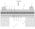
side operation)のために、図1Aの例示的な構造に例示される層は、基板24の上に逆の順序で配置されてよい。

11 第5の遮蔽層(fifth dielectric shielding layer)
12 光学的に整合する誘電体層(optically matching dielectric layer)
13 第4の誘電体遮蔽層(fourth dielectric shielding layer)
14 第3の誘電体遮蔽層(third dielectric shielding layer)
15 半透明金属層(semi−transparent metal layer)
17 自己支持誘電体遮蔽層(self−supporting dielectric shielding layer)
20 発熱抵抗体配線(heating resistor wiring)
21 コンタクト端子(contact terminal)
22 コンタクト端子(contact terminal)
24 シリコン基板(silicon substrate)
25 中央開口(central opening)
Claims (12)
- 2つ又はそれよりも多くの誘電体層の間に積み重ねられた少なくとも1つの金属層と、該少なくとも1つの金属層を所要の赤外線放射温度まで加熱するために、前記誘電体層のいずれかの内に又は間に配置される、電気加熱手段とを有する、層状構造を含み、
該層状構造内の各金属層は、半透明金属層であり、
前記誘電体層のうちの少なくとも1つは、前記少なくとも1つの半透明金属層を前記層状構造の放射外面に光学的に整合させるように構成され、該少なくとも1つの光学的に整合する誘電体層は、前記半透明金属層と前記放射外面との間に配置され、前記少なくとも1つの光学的に整合する誘電体層は、ポリシリコン材料又は高い屈折率を有する他の誘電体材料で作られる、
層状赤外線エミッタデバイス。 - 前記層状構造は、1つだけの金属層を含む、請求項1に記載の層状赤外線エミッタデバイス。
- 前記半透明金属層の厚さは、2nm〜50nmの範囲、3nm〜20nmの範囲、及び5nm〜15nmの範囲で構成される群から選択される、請求項1に記載の層状赤外線エミッタデバイス。
- 前記半透明金属層は、熱的に安定した金属で作られ、該金属は、モリブデン、タングステン、チタン、タンタル、パラジウム、白金、及びニオブで構成される群から選択される、請求項1に記載の層状赤外線エミッタデバイス。
- 前記少なくとも1つの光学的に整合する誘電体層の厚さは、前記少なくとも1つの半透明金属層の厚さよりも数倍大きい、請求項1に記載の層状赤外線エミッタデバイス。
- 前記誘電体層は、前記少なくとも1つの半透明層を取り囲んで、前記層状構造の他の層との並びに周囲の作用物質との化学反応を防止するように構成される、遮蔽層を含む、請求項1に記載の層状赤外線エミッタデバイス。
- 前記誘電体層は、前記層状構造の異なる層の間の並びに周囲の作用物質との化学反応を防止するように構成される遮蔽層を含み、該遮蔽層のうちの少なくとも1つは、窒化ケイ素、多結晶、及び酸化アルミニウムを含む金属酸化物で構成される群から選択される材料で作られる、請求項1に記載の層状赤外線エミッタデバイス。
- 前記層状構造は、放射側から反対側への順序において、
少なくとも1つの遮蔽誘電体層と、
高い屈折率を有する光学的に整合する誘電体層と、
少なくとも1つの遮蔽誘電体層と、
前記半透明金属層と、
少なくとも1つの遮蔽誘電体層とを含み、
前記電気加熱手段は、前記遮蔽誘電体層の内に又は間に配置される、
請求項1に記載の層状赤外線エミッタデバイス。 - 前記層状構造は、放射側から反対側への順序において、
第1の遮蔽誘電体層と、
高い屈折率を有する光学的に整合する誘電体層と、
第2の遮蔽誘電体層と、
第3の遮蔽誘電体層と、
前記層状構造における唯一の金属層である前記半透明金属層と、
第4の遮蔽誘電体層と、
第5の遮蔽誘電体層と、
前記遮蔽誘電体層のいずれか1つの内に又は間に配置される前記電気加熱手段とを含む、
請求項1に記載の層状赤外線エミッタデバイス。 - 前記所要の赤外線放射温度は、400℃〜1000℃の範囲内にある、請求項1に記載の赤外線エミッタデバイス。
- 分光学的又はNDIR気体、液体若しくは固体物質測定のための赤外線エミッタデバイスの使用であって、
該赤外線エミッタデバイスは、2つ又はそれよりも多くの誘電体層の間に積み重ねられた少なくとも1つの金属層と、該少なくとも1つの金属層を所要の赤外線放射温度まで加熱するために、前記誘電体層のいずれかの内に又は間に配置される、電気加熱手段とを有する、層状構造を含み、該層状構造内の各金属層は、半透明金属層であり、
前記誘電体層のうちの少なくとも1つは、前記少なくとも1つの半透明金属層を前記層状構造の放射外面に光学的に整合させるように構成され、該少なくとも1つの光学的に整合する誘電体層は、前記半透明金属層と前記放射外面との間に配置され、前記少なくとも1つの光学的に整合する誘電体層は、ポリシリコン材料又は高い屈折率を有する他の誘電体材料で作られる、
使用。 - 前記所要の赤外線放射温度は、400℃〜1000℃の範囲内にある、請求項11に記載の使用。
Applications Claiming Priority (2)
| Application Number | Priority Date | Filing Date | Title |
|---|---|---|---|
| FI20165816A FI127446B (en) | 2016-10-28 | 2016-10-28 | Infrared transmitter with layered structure |
| FI20165816 | 2016-10-28 |
Publications (2)
| Publication Number | Publication Date |
|---|---|
| JP2018073812A JP2018073812A (ja) | 2018-05-10 |
| JP6543674B2 true JP6543674B2 (ja) | 2019-07-10 |
Family
ID=60190660
Family Applications (1)
| Application Number | Title | Priority Date | Filing Date |
|---|---|---|---|
| JP2017193254A Active JP6543674B2 (ja) | 2016-10-28 | 2017-10-03 | 層状構造を有する赤外線エミッタ |
Country Status (5)
| Country | Link |
|---|---|
| US (1) | US10001409B2 (ja) |
| EP (1) | EP3315929B1 (ja) |
| JP (1) | JP6543674B2 (ja) |
| CN (1) | CN108012357B (ja) |
| FI (1) | FI127446B (ja) |
Families Citing this family (10)
| Publication number | Priority date | Publication date | Assignee | Title |
|---|---|---|---|---|
| DE102015119763A1 (de) * | 2015-11-16 | 2017-05-18 | Heraeus Quarzglas Gmbh & Co. Kg | Infrarotstrahler |
| US10680150B2 (en) * | 2017-08-15 | 2020-06-09 | Dragan Grubisik | Electrically conductive-semitransparent solid state infrared emitter apparatus and method of use thereof |
| EP3462149B1 (en) | 2017-09-28 | 2023-10-25 | Sensirion AG | Infrared device |
| US11402272B2 (en) | 2018-11-07 | 2022-08-02 | Teknologian Tutkimuskeskus Vtt Oy | Absorber structure for thermal detectors |
| EP3696523A1 (de) * | 2019-02-12 | 2020-08-19 | Hahn-Schickard-Gesellschaft für angewandte Forschung e.V. | Ir-emitter mit modulierbarem emissionsgrad auf basis von metamaterialien |
| EP3938747A2 (en) | 2019-03-11 | 2022-01-19 | Flir Commercial Systems, Inc. | Microbolometer systems and methods |
| CN111006773B (zh) * | 2019-11-26 | 2022-02-11 | 北京振兴计量测试研究所 | 一种空间环境下的mems红外辐射面均匀性提升系统 |
| US12106957B2 (en) * | 2020-04-30 | 2024-10-01 | Taiwan Nano & Micro-Photonics Co., Ltd. | Narrow band infrared emitter through thermal manner |
| JP7456903B2 (ja) | 2020-09-18 | 2024-03-27 | 旭化成エレクトロニクス株式会社 | 受発光装置 |
| FI130930B1 (fi) | 2021-08-02 | 2024-05-31 | Teknologian Tutkimuskeskus Vtt Oy | Laite ei-invasiiviseen seurantaan |
Family Cites Families (10)
| Publication number | Priority date | Publication date | Assignee | Title |
|---|---|---|---|---|
| JPH02284377A (ja) * | 1989-04-25 | 1990-11-21 | Unitika Ltd | 遠赤外線放射性透明面状発熱体 |
| JPH05266965A (ja) * | 1992-03-19 | 1993-10-15 | Satako Eng:Kk | 遠赤外線放射積層体 |
| FI112005B (fi) | 1995-11-24 | 2003-10-15 | Valtion Teknillinen | Sähköisesti moduloitavissa oleva terminen säteilylähde |
| WO2002080620A1 (en) | 2001-03-28 | 2002-10-10 | Ecole Polytechnique Federale De Lausanne (Epfl) | High temperature micro-hotplate |
| WO2006086117A2 (en) * | 2005-01-13 | 2006-08-17 | Massachusetts Institute Of Technology | Vertical-cavity enhanced resonant thermal emitter |
| JP5243817B2 (ja) * | 2008-02-29 | 2013-07-24 | パナソニック株式会社 | 赤外線放射素子 |
| US8859303B2 (en) | 2010-01-21 | 2014-10-14 | Cambridge Cmos Sensors Ltd. | IR emitter and NDIR sensor |
| JP2013017013A (ja) * | 2011-07-04 | 2013-01-24 | Seiko Epson Corp | 赤外線送信機及びプロジェクションシステム |
| WO2013168332A1 (ja) | 2012-05-09 | 2013-11-14 | パナソニック株式会社 | 赤外線放射素子 |
| US9733404B2 (en) | 2012-09-06 | 2017-08-15 | Vaisala Oyj | Layered structure for an infrared emitter, infrared emitter device and detector |
-
2016
- 2016-10-28 FI FI20165816A patent/FI127446B/en active
-
2017
- 2017-09-29 US US15/720,079 patent/US10001409B2/en active Active
- 2017-10-03 JP JP2017193254A patent/JP6543674B2/ja active Active
- 2017-10-26 EP EP17198638.3A patent/EP3315929B1/en active Active
- 2017-10-26 CN CN201711017933.1A patent/CN108012357B/zh active Active
Also Published As
| Publication number | Publication date |
|---|---|
| CN108012357A (zh) | 2018-05-08 |
| FI20165816L (fi) | 2018-04-29 |
| EP3315929B1 (en) | 2024-03-27 |
| US10001409B2 (en) | 2018-06-19 |
| FI20165816A7 (fi) | 2018-04-29 |
| US20180120158A1 (en) | 2018-05-03 |
| JP2018073812A (ja) | 2018-05-10 |
| EP3315929C0 (en) | 2024-03-27 |
| CN108012357B (zh) | 2020-09-22 |
| EP3315929A1 (en) | 2018-05-02 |
| FI127446B (en) | 2018-06-15 |
Similar Documents
| Publication | Publication Date | Title |
|---|---|---|
| JP6543674B2 (ja) | 層状構造を有する赤外線エミッタ | |
| US9733404B2 (en) | Layered structure for an infrared emitter, infrared emitter device and detector | |
| JP6316955B2 (ja) | 異方性熱電材料を利用するレーザーパワーおよびエネルギーセンサ | |
| WO2010150787A1 (ja) | 赤外線式ガス検知器および赤外線式ガス計測装置 | |
| JPWO2016031547A1 (ja) | 電磁波吸収及び輻射材料及びその製造方法並びに赤外線源 | |
| JP6868908B2 (ja) | 構造化シリコンベース熱エミッタ | |
| Guo et al. | Touchless thermosensation enabled by flexible infrared photothermoelectric detector for temperature prewarning function of electronic skin | |
| Konz et al. | Micromachined IR-source with excellent blackbody like behaviour | |
| JP5506514B2 (ja) | 赤外光源 | |
| JP2016065786A (ja) | 赤外線放射素子、及びその製造方法、並びにガス分析装置 | |
| JP7596130B2 (ja) | 電磁波センサ | |
| Svatoš et al. | In situ observation of carbon nanotube layer growth on microbolometers with substrates at ambient temperature | |
| JP5442648B2 (ja) | 赤外線センサ | |
| US8823250B2 (en) | High efficiency incandescent lighting | |
| CN114144643A (zh) | 监测辐射的方法和设备 | |
| WO2009086211A2 (en) | Shaped selective thermal emitter | |
| Li et al. | High‐Accuracy and Broadband Wavelength Sensor with Detection Region Ranging from Deep Ultraviolet to Near Infrared Light | |
| US20240285172A1 (en) | A device for non-invasive monitoring | |
| TWI860544B (zh) | 熱輻射感測器和溫度感測單元的製造方法 | |
| Liao et al. | MEMS-Based Planar Incandescent Microfilaments With Low Voltage Operation | |
| KR20180010059A (ko) | 온도 센서 | |
| Chernin | High-temperature miniature blackbody radiation sources | |
| JP2023033863A (ja) | 構造体及び電磁波センサ | |
| JP2018009898A (ja) | 測定セル及びガス分析装置 | |
| KR101410079B1 (ko) | 면상발열식 ndir 가스센서 |
Legal Events
| Date | Code | Title | Description |
|---|---|---|---|
| A131 | Notification of reasons for refusal |
Free format text: JAPANESE INTERMEDIATE CODE: A131 Effective date: 20180313 |
|
| A521 | Request for written amendment filed |
Free format text: JAPANESE INTERMEDIATE CODE: A523 Effective date: 20180606 |
|
| A131 | Notification of reasons for refusal |
Free format text: JAPANESE INTERMEDIATE CODE: A131 Effective date: 20180911 |
|
| A601 | Written request for extension of time |
Free format text: JAPANESE INTERMEDIATE CODE: A601 Effective date: 20181210 |
|
| A601 | Written request for extension of time |
Free format text: JAPANESE INTERMEDIATE CODE: A601 Effective date: 20190208 |
|
| A521 | Request for written amendment filed |
Free format text: JAPANESE INTERMEDIATE CODE: A523 Effective date: 20190308 |
|
| TRDD | Decision of grant or rejection written | ||
| A01 | Written decision to grant a patent or to grant a registration (utility model) |
Free format text: JAPANESE INTERMEDIATE CODE: A01 Effective date: 20190611 |
|
| A61 | First payment of annual fees (during grant procedure) |
Free format text: JAPANESE INTERMEDIATE CODE: A61 Effective date: 20190617 |
|
| R150 | Certificate of patent or registration of utility model |
Ref document number: 6543674 Country of ref document: JP Free format text: JAPANESE INTERMEDIATE CODE: R150 |
|
| R250 | Receipt of annual fees |
Free format text: JAPANESE INTERMEDIATE CODE: R250 |
|
| R250 | Receipt of annual fees |
Free format text: JAPANESE INTERMEDIATE CODE: R250 |
|
| R250 | Receipt of annual fees |
Free format text: JAPANESE INTERMEDIATE CODE: R250 |
|
| R250 | Receipt of annual fees |
Free format text: JAPANESE INTERMEDIATE CODE: R250 |