JP6522666B2 - On-Chip Dual-Supply Multi-Mode CMOS Regulator - Google Patents
On-Chip Dual-Supply Multi-Mode CMOS Regulator Download PDFInfo
- Publication number
- JP6522666B2 JP6522666B2 JP2016569919A JP2016569919A JP6522666B2 JP 6522666 B2 JP6522666 B2 JP 6522666B2 JP 2016569919 A JP2016569919 A JP 2016569919A JP 2016569919 A JP2016569919 A JP 2016569919A JP 6522666 B2 JP6522666 B2 JP 6522666B2
- Authority
- JP
- Japan
- Prior art keywords
- regulator
- voltage
- voltage regulator
- circuit
- vco
- Prior art date
- Legal status (The legal status is an assumption and is not a legal conclusion. Google has not performed a legal analysis and makes no representation as to the accuracy of the status listed.)
- Active
Links
Images


Classifications
-
- G—PHYSICS
- G05—CONTROLLING; REGULATING
- G05F—SYSTEMS FOR REGULATING ELECTRIC OR MAGNETIC VARIABLES
- G05F1/00—Automatic systems in which deviations of an electric quantity from one or more predetermined values are detected at the output of the system and fed back to a device within the system to restore the detected quantity to its predetermined value or values, i.e. retroactive systems
- G05F1/10—Regulating voltage or current
- G05F1/46—Regulating voltage or current wherein the variable actually regulated by the final control device is dc
- G05F1/56—Regulating voltage or current wherein the variable actually regulated by the final control device is dc using semiconductor devices in series with the load as final control devices
- G05F1/575—Regulating voltage or current wherein the variable actually regulated by the final control device is dc using semiconductor devices in series with the load as final control devices characterised by the feedback circuit
-
- H—ELECTRICITY
- H02—GENERATION; CONVERSION OR DISTRIBUTION OF ELECTRIC POWER
- H02M—APPARATUS FOR CONVERSION BETWEEN AC AND AC, BETWEEN AC AND DC, OR BETWEEN DC AND DC, AND FOR USE WITH MAINS OR SIMILAR POWER SUPPLY SYSTEMS; CONVERSION OF DC OR AC INPUT POWER INTO SURGE OUTPUT POWER; CONTROL OR REGULATION THEREOF
- H02M1/00—Details of apparatus for conversion
- H02M1/0067—Converter structures employing plural converter units, other than for parallel operation of the units on a single load
- H02M1/0077—Plural converter units whose outputs are connected in series
-
- H—ELECTRICITY
- H02—GENERATION; CONVERSION OR DISTRIBUTION OF ELECTRIC POWER
- H02M—APPARATUS FOR CONVERSION BETWEEN AC AND AC, BETWEEN AC AND DC, OR BETWEEN DC AND DC, AND FOR USE WITH MAINS OR SIMILAR POWER SUPPLY SYSTEMS; CONVERSION OF DC OR AC INPUT POWER INTO SURGE OUTPUT POWER; CONTROL OR REGULATION THEREOF
- H02M3/00—Conversion of dc power input into dc power output
- H02M3/02—Conversion of dc power input into dc power output without intermediate conversion into ac
- H02M3/04—Conversion of dc power input into dc power output without intermediate conversion into ac by static converters
- H02M3/10—Conversion of dc power input into dc power output without intermediate conversion into ac by static converters using discharge tubes with control electrode or semiconductor devices with control electrode
- H02M3/145—Conversion of dc power input into dc power output without intermediate conversion into ac by static converters using discharge tubes with control electrode or semiconductor devices with control electrode using devices of a triode or transistor type requiring continuous application of a control signal
- H02M3/155—Conversion of dc power input into dc power output without intermediate conversion into ac by static converters using discharge tubes with control electrode or semiconductor devices with control electrode using devices of a triode or transistor type requiring continuous application of a control signal using semiconductor devices only
- H02M3/156—Conversion of dc power input into dc power output without intermediate conversion into ac by static converters using discharge tubes with control electrode or semiconductor devices with control electrode using devices of a triode or transistor type requiring continuous application of a control signal using semiconductor devices only with automatic control of output voltage or current, e.g. switching regulators
Description
[0001]本願は、2014年5月30日に出願された「ON-CHIP DUAL-SUPPLY MULTI-MODE CMOS REGULATORS」と題する米国特許仮出願第62/005,765号及び2015年2月24日に出願された「ON-CHIP DUAL-SUPPLY MULTI-MODE CMOS REGULATORS」と題する米国特許出願第14/630,506号の利益を主張し、それらは、参照によって全体が本明細書に明確に組み込まれる。 [0001] This application claims the benefit of US Provisional Patent Application Ser. No. 62 / 005,765 entitled “ON-CHIP DUAL-SUPPLY MULTI-MODE CMOS REGULATORS” filed May 30, 2014 and Feb. 24, 2015. This application claims the benefit of US patent application Ser. No. 14 / 630,506, entitled “ON-CHIP DUAL-SUPPLY MULTI-MODE CMOS REGULATORS,” which are expressly incorporated herein by reference in their entirety.
[0002]本開示は一般に、通信システムに関し、より詳細には、電圧制御型発振器(VCO)のための電圧レギュレータに関する。 FIELD [0002] The present disclosure relates generally to communication systems, and more particularly to voltage regulators for voltage controlled oscillators (VCOs).
[0003]ワイヤレスデバイス(例えば、セルラ電話又はスマートフォン)は、ワイヤレス通信システムとの双方向通信ためにデータを送信及び受信し得る。ワイヤレスデバイスは、データ送信用の送信機と、データ受信用の受信機とを含み得る。データ送信では、送信機は、送信局部発振器(LO)信号をデータで変調して、変調された無線周波数(RF)信号を取得し、変調されたRF信号を増幅して所望の出力レベルを有する出力RF信号を取得し、それらの出力RF信号をアンテナを介して基地局に送信し得る。データ受信では、受信機は、アンテナを介して受信RF信号を取得し、受信RF信号を受信LO信号で増幅及びダウンコンバートし、ダウンコンバートされた信号を処理して、基地局によって送られたデータを復元し得る。 A wireless device (eg, a cellular telephone or smartphone) may transmit and receive data for two-way communication with a wireless communication system. The wireless device may include a transmitter for data transmission and a receiver for data reception. For data transmission, the transmitter modulates a transmit local oscillator (LO) signal with data to obtain a modulated radio frequency (RF) signal and amplifies the modulated RF signal to have a desired output level The output RF signals may be obtained and transmitted to the base station via the antennas. For data reception, the receiver obtains the received RF signal via the antenna, amplifies and downconverts the received RF signal with the received LO signal, processes the downconverted signal, and sends the data sent by the base station Can be restored.
[0004]ワイヤレスデバイスは、1つ又は複数の所望の周波数において1つ又は複数の発振信号を生成するために1つ又は複数の発振器を含み得る。発振信号は、送信機用の送信LO信号及び受信機用のLO信号を生成するために使用され得る。発振器は、ワイヤレスデバイスが通信するワイヤレス通信システムの要件を満たすために発振信号を生成する必要があり得る。 A wireless device may include one or more oscillators to generate one or more oscillating signals at one or more desired frequencies. The oscillating signal may be used to generate a transmit LO signal for the transmitter and an LO signal for the receiver. The oscillator may need to generate an oscillating signal to meet the requirements of the wireless communication system with which the wireless device communicates.
[0005]VCOは、送信LO信号及び受信LO信号を生成するために使用される。VCOは一般に、VCOへの入力電圧を提供するレギュレータに接続される。VCOの性能は、レギュレータに依存し得る。従って、VCOのための効率的なレギュレータが、最適性能及び低ノイズのために望まれる。 [0005] A VCO is used to generate the transmit LO signal and the receive LO signal. The VCO is generally connected to a regulator that provides an input voltage to the VCO. The performance of the VCO may depend on the regulator. Thus, an efficient regulator for the VCO is desired for optimal performance and low noise.
[0006]本開示のある態様では、方法及び装置が提供される。装置は、レギュレータ回路であり得る。レギュレータ回路は、第1の電圧レギュレータへの第1の入力電圧を調整するための第1の電圧レギュレータと、ここで、第1の電圧レギュレータは、P型金属酸化膜半導体(PMOS)を含み、第2の電圧レギュレータへの第2の入力電圧を調整するための第2の電圧レギュレータと、ここで、第2の電圧レギュレータは、N型金属酸化膜半導体(NMOS)を含み、を含む。ある態様では、第1の電圧レギュレータは、第2の電圧レギュレータに結合される。ある態様では、レギュレータ回路は、第1の電圧レギュレータ又は第2の電圧レギュレータのうちの少なくとも1つを選択的にアクティブにするための切替え回路を更に含み得る。ある態様では、第1の電圧レギュレータ及び第2の電圧レギュレータは、直列に接続される。ある態様では、第1の電圧レギュレータ及び第2の電圧レギュレータは、並列に接続される。ある態様では、第1の電圧レギュレータは、2つの段において第1の入力電圧を増幅するための二段式増幅器回路を含む。ある態様では、第2の電圧レギュレータ回路は、2つの段において第2の入力電圧を増幅するための二段式増幅器回路を含む。ある態様では、第2の電圧レギュレータは、ポールキャンセレーション回路(pole-cancelation circuit)を含む。ある態様では、第2の電圧レギュレータは、キャパシタ及び抵抗器を含み、抵抗器の一端は、キャパシタに接続され、抵抗器の別の端は、NMOSのソースに接続される。ある態様では、第1の電圧レギュレータ及び第2の電圧レギュレータは、入力電圧調整の程度(degree)を変更するように調節可能(tunable)である。 [0006] In an aspect of the present disclosure, a method and apparatus are provided. The device may be a regulator circuit. The regulator circuit comprises a first voltage regulator for regulating a first input voltage to a first voltage regulator, wherein the first voltage regulator comprises a P-type metal oxide semiconductor (PMOS), A second voltage regulator for regulating a second input voltage to a second voltage regulator, wherein the second voltage regulator comprises an N-type metal oxide semiconductor (NMOS). In one aspect, a first voltage regulator is coupled to a second voltage regulator. In one aspect, the regulator circuit may further include a switching circuit for selectively activating at least one of the first voltage regulator or the second voltage regulator. In one aspect, the first voltage regulator and the second voltage regulator are connected in series. In one aspect, the first voltage regulator and the second voltage regulator are connected in parallel. In one aspect, the first voltage regulator includes a two-stage amplifier circuit for amplifying a first input voltage in two stages. In one aspect, the second voltage regulator circuit includes a two-stage amplifier circuit for amplifying a second input voltage in two stages. In one aspect, the second voltage regulator includes a pole-cancelation circuit. In one aspect, the second voltage regulator includes a capacitor and a resistor, wherein one end of the resistor is connected to the capacitor and the other end of the resistor is connected to the source of the NMOS. In one aspect, the first voltage regulator and the second voltage regulator are tunable to change the degree of input voltage regulation.
[0022]添付の図面に関連して以下に示される詳細な説明は、様々な構成の説明を意図しており、本明細書で説明される概念が実施され得る唯一の構成を表すことを意図したものではない。詳細な説明は、様々な概念の完全な理解を提供するために特定の詳細を含む。しかしながら、これらの概念がこれらの特定の詳細なしに実施され得ることは当業者には明らかとなるであろう。幾つかの事例では、そのような概念を曖昧にしないために、周知の構造及び構成要素がブロック図の形式で示される。「例示的」という用語は、本明細書では、「実例、事例、又は例示としての役割を果たす」という意味で使用される。「例示的」として本明細書で説明される任意の設計は、必ずしも、他の設計よりも好ましい又は有利であると解釈されるべきではない。 [0022] The detailed description set forth below in connection with the appended drawings is intended to describe various configurations and is intended to represent the only configurations in which the concepts described herein may be practiced. It is not something that The detailed description includes specific details to provide a thorough understanding of the various concepts. However, it will be apparent to one skilled in the art that these concepts may be practiced without these specific details. In some instances, well-known structures and components are shown in block diagram form in order not to obscure such concepts. The term "exemplary" is used herein to mean "serving as an example, instance, or illustration." Any design described herein as "exemplary" is not necessarily to be construed as preferred or advantageous over other designs.
[0023]電気通信システムの幾つかの態様が、これより、様々な装置及び方法に関連して提示されるであろう。これらの装置及び方法は、以下の詳細な説明で説明され、様々なブロック、モジュール、構成要素、回路、ステップ、プロセス、アルゴリズム、等(総称して「要素」と呼ばれる)によって添付の図面で例示されるだろう。これらの要素は、電子ハードウェア、コンピュータソフトウェア、又はそれらの任意の組み合わせを使用して実装され得る。そのような要素がハードウェアとして実装されるかソフトウェアとして実装されるかは、特定の用途及びシステム全体に課される設計制約に依存する。 [0023] Several aspects of the telecommunication system will now be presented in connection with various apparatuses and methods. These devices and methods are described in the following detailed description and are illustrated in the accompanying drawings by the various blocks, modules, components, circuits, steps, processes, algorithms, etc. (collectively referred to as "elements") It will be done. These elements may be implemented using electronic hardware, computer software, or any combination thereof. Whether such elements are implemented as hardware or software depends upon the particular application and design constraints imposed on the overall system.
[0024]例として、1つの要素、又は1つの要素の任意の部分若しくは複数の要素の任意の組み合わせが、1つ又は複数のプロセッサを含む「処理システム」を用いて実装され得る。プロセッサの例には、マイクロプロセッサ、マイクロコントローラ、デジタルシグナルプロセッサ(DSP)、フィールドプログラマブルゲートアレイ(FPGA)、プログラマブル論理デバイス(PLD)、ステートマシン、ゲートロジック、ディスクリートハードウェア回路及び本開示全体を通して説明される様々な機能性を実行するように構成された他の適切なハードウェアが含まれる。処理システム内の1つ又は複数のプロセッサはソフトウェアを実行し得る。ソフトウェアは、ソフトウェア、ファームウェア、ミドルウェア、マイクロコード、ハードウェア記述言語と呼ばれても、それ以外の名称で呼ばれても、命令、命令のセット、コード、コードセグメント、プログラムコード、プログラム、サブプログラム、ソフトウェアモジュール、アプリケーション、ソフトウェアアプリケーション、ソフトウェアパッケージ、ルーチン、サブルーチン、オブジェクト、実行ファイル、実行スレッド、プロシージャ、関数、等を意味すると広く解釈されるものとする。 [0024] As an example, an element, or any portion of an element or any combination of elements may be implemented with a "processing system" that includes one or more processors. Examples of processors include microprocessors, microcontrollers, digital signal processors (DSPs), field programmable gate arrays (FPGAs), programmable logic devices (PLDs), state machines, gate logic, discrete hardware circuits and throughout the disclosure. And other suitable hardware configured to perform the various functionalities that are performed. One or more processors in the processing system may execute software. Software may be called software, firmware, middleware, microcode, hardware description language, or anything else called instructions, sets of instructions, codes, code segments, program codes, programs, subprograms , Software modules, applications, software applications, software packages, routines, subroutines, objects, executables, threads of execution, procedures, functions, etc. shall be interpreted broadly.
[0025]従って、1つ又は複数の例示的な実施形態では、説明される機能は、ハードウェア、ソフトウェア、ファームウェア、又はこれらの任意の組み合わせに実装され得る。ソフトウェアに実装される場合、これらの機能は、コンピュータ読取可能な媒体上の1つ又は複数の命令又はコードとして記憶又は符号化され得る。コンピュータ読取可能な媒体はコンピュータ記憶媒体を含む。記憶媒体は、コンピュータによりアクセスされることができる任意の利用可能な媒体であり得る。限定ではなく例として、このようなコンピュータ読取可能な媒体は、ランダムアクセスメモリ(RAM)、読取専用メモリ(ROM)、電気的消去可能プログラマブルROM(EEPROM(登録商標))、コンパクトディスク(CD)ROM(CD−ROM)又は他の光ディスク記憶装置、磁気ディスク記憶装置又は他の磁気記憶デバイス若しくはデータ構造又は命令の形式で所望のプログラムコードを搬送若しくは記憶するために使用されることができ、かつコンピュータによってアクセスされることができる任意の他の媒体を備えることができる。本明細書で使用される場合、ディスク(disk)及びディスク(disc)は、CD、レーザーディスク(登録商標)、光ディスク、デジタル多用途ディスク(DVD)、及びフロッピー(登録商標)ディスクを含み、ここで、ディスク(disk)は、通常磁気的にデータを再生し、ディスク(disc)は、レーザーを用いて光学的にデータを再生する。上記の組み合わせもまた、コンピュータ読取可能な媒体の範囲内に含まれるべきである。 Thus, in one or more exemplary embodiments, the functions described may be implemented in hardware, software, firmware, or any combination thereof. When implemented in software, these functions may be stored or encoded as one or more instructions or code on a computer readable medium. Computer-readable media includes computer storage media. A storage media may be any available media that can be accessed by a computer. By way of example and not limitation, such computer readable media may be random access memory (RAM), read only memory (ROM), electrically erasable programmable ROM (EEPROM), compact disc (CD) ROM. (CD-ROM) or other optical disk storage device, magnetic disk storage device or other magnetic storage device or data structure or data structure or instruction can be used to carry or store desired program code, and computer Can comprise any other medium that can be accessed by As used herein, discs and discs include CDs, laser discs, optical discs, digital versatile discs (DVDs), and floppy discs. The disc normally reproduces data magnetically, and the disc reproduces data optically using a laser. Combinations of the above should also be included within the scope of computer readable media.
[0026]図1は、異なるワイヤレス通信システム120,122と通信するワイヤレスデバイス110を例示する図100である。ワイヤレス通信システム120,122は各々、符号分割多元接続(CDMA)システム、モバイル通信のためのグローバルシステム(GSM(登録商標))システム、ロングタームエボリューション(LTE(登録商標))システム、ワイヤレスローカルエリアネットワーク(WLAN)システム又は何等かの他のワイヤレスシステムであり得る。CDMAシステムは、広帯域CDMA(WCDMA(登録商標))、CDMA 1X又はcdma2000、時分割同期符号分割多元接続(TD−SCDMA)又は他の何等かのバージョンのCDMAを実装し得る。TD−SCDMAは、ユニバーサル地上無線アクセス(UTRA)時分割複信(TDD)1.28Mcpsオプション又は低チップレート(LCR)とも呼ばれる。LTEは、周波数分割複信(FDD)及び時分割複信(TDD)の両方をサポートする。例えば、ワイヤレス通信システム120は、GSMシステムであり得、ワイヤレス通信システム122は、WCDMAシステムであり得る。別の例として、ワイヤレス通信システム120は、LTEシステムであり得、ワイヤレス通信システム122は、CDMAシステムであり得る。
[0026] FIG. 1 is a diagram 100 illustrating
[0027]簡単化のために、図100は、1つの基地局130及び1つのシステムコントローラ140を含むワイヤレス通信システム120と、1つの基地局132及び1つのシステムコントローラ142を含むワイヤレス通信システム122とを示す。一般に、各ワイヤレスシステムは、任意の数の基地局及び任意のセットのネットワークエンティティを含み得る。各基地局は、その基地局のカバレッジ内のワイヤレスデバイスのための通信をサポートし得る。基地局は、ノードB、発展型ノードB(eNB)、アクセスポイント、トランシーバ基地局、無線基地局、無線トランシーバ、トランシーバ機能、基本サービスセット(BSS)、拡張サービスセット(ESS)又は何等かの他の適切な用語でも呼ばれ得る。ワイヤレスデバイス110は、ユーザ機器(UE)、モバイルデバイス、リモートデバイス、ワイヤレスデバイス、ワイヤレス通信デバイス、局、モバイル局、加入者局、モバイル加入者局、端末、モバイル端末、リモート端末、ワイヤレス端末、アクセス端末、クライント、モバイルクライアント、モバイルユニット、加入者ユニット、ワイヤレスユニット、リモートユニット、ハンドセット、ユーザエージェント又は何等かの他の適切な用語でも呼ばれ得る。ワイヤレスデバイス110は、セルラ電話、スマートフォン、タブレット、ワイヤレスモデム、携帯情報端末(PDA)、ハンドヘルドデバイス、ラップトップコンピュータ、スマートブック、ネットブック、コードレス電話、ワイヤレスローカルループ(WLL)局又は何等かの他の同様に機能するデバイスであり得る。
[0027] For simplicity, the diagram 100 illustrates a
[0028]ワイヤレスデバイス110は、ワイヤレス通信システム120及び/又は122と通信することが可能であり得る。ワイヤレスデバイス110はまた、ブロードキャスト局134のようなブロードキャスト局から信号を受信することが可能であり得る。ワイヤレスデバイス110はまた、1つ又は複数の全地球的航法衛星システム(GNSS)において、衛星150のような衛星から信号を受信することが可能であり得る。ワイヤレスデバイス110は、GSM、WCDMA、cdma2000、LTE、802.11、等のような、ワイヤレス通信のための1つ又は複数の無線技術をサポートし得る。「無線技術」、「無線接続技術」、「エアインターフェース」及び「規格」という用語は、交換可能に使用され得る。
[0029]ワイヤレスデバイス110は、ダウンリンク及びアップリンクを介してワイヤレスシステムにおける基地局と通信し得る。ダウンリンク(即ち、順方向リンク)は、基地局からワイヤレスデバイスへの通信リンクを指し、アップリンク(即ち、逆方向リンク)は、ワイヤレスデバイスから基地局への通信リンクを指す。ワイヤレスシステムは、TDD及び/又はFDDを利用し得る。TDDの場合、ダウンリンク及びアップリンクは、同じ周波数を共有し、ダウンリンク送信及びアップリンク送信は、異なる時間期間において同じ周波数上で送られ得る。FDDの場合、ダウンリンク及びアップリンクは、個別の周波数が割り振られ得る。ダウンリンク送信は、ある周波数上で送られ、アップリンク送信は、別の周波数上で送られ得る。TDDをサポートする幾つかの例示的な無線技術には、GSM、LTE及びTD−SCDMAが含まれる。FDDをサポートする幾つかの例示的な無線技術には、WCDMA、cdma2000及びLTEが含まれる。ワイヤレスデバイス110及び/又は基地局130,132は、例示的なVCOレギュレータ160を含み得る。VCOレギュレータ160が以下に提供される。
[0030]図2は、ワイヤレスデバイス110のような例示的なワイヤレスデバイスのブロック図200である。ワイヤレスデバイスは、データプロセッサ/コントローラ210、トランシーバ218及びアンテナ290を含む。データプロセッサ/コントローラ210は、処理システムと呼ばれ得る。処理システムは、データプロセッサ/コントローラ210を、又は、データプロセッサ/コントローラ210及びメモリ216の両方を含み得る。トランシーバ218は、双方向通信をサポートする送信機220及び受信機250を含む。送信機220及び/又は受信機250は、スーパーヘテロダインアーキテクチャ又はダイレクト変換アーキテクチャで実装され得る。スーパーヘテロダインアーキテクチャでは、信号は、複数の段においてRFとベースバンドとの間で、例えば、1つの段でRFから中間周波数(IF)に、その後、受信機のために別の段でIFからベースバンドに周波数変換される。ゼロIFアーキテクチャとも呼ばれる、ダイレクト変換アーキテクチャでは、信号は、1つの段においてRFとベースバンドとの間で周波数変換される。スーパーヘテロダイン及びダイレクト変換アーキテクチャは、異なる回路ブロックを使用し得る、及び/又は、異なる要件を有し得る。図2に示される例示的な設計では、送信機220及び受信機250は、ダイレクト変換アーキテクチャで実装される。
[0030] FIG. 2 is a block diagram 200 of an exemplary wireless device, such as
[0031]送信経路では、データプロセッサ/コントローラ210は、送信されるべきデータを処理(例えば、符号化及び変調)し、このデータをデジタル/アナログ変換器(DAC)230に供給し得る。DAC230は、デジタル入力信号をアナログ出力信号へと変換する。アナログ出力信号は、DAC230による前のデジタル/アナログ変換によってもたらされるイメージを除去するためにこのアナログ出力信号をフィルタに掛け得る送信(TX)ベースバンド(ローパス)フィルタ232に供給される。増幅器(amp)234は、TXベースバンドフィルタ232からの信号を増幅し、増幅されたベースバンド信号を供給し得る。アップコンバータ(ミキサ)236は、増幅されたベースバンド信号と、TX LO信号ジェネレータ276からのTX LO信号とを受け得る。アップコンバータ236は、増幅されたベースバンド信号をTX LO信号でアップコンバートし、アップコンバートされた信号を供給し得る。フィルタ238は、周波数アップコンバージョンによってもたらされたイメージを除去するために、アップコンバートされた信号をフィルタに掛け得る。電力増幅器(PA)240は、フィルタ238からのフィルタに掛けられたRF信号を増幅して、所望の出力電力レベルを取得し、出力RF信号を供給する。出力RF信号は、デュプレクサ/スイッチプレクサ264を通してルーティングされ得る。
[0031] In the transmit path, data processor /
[0032]FDDの場合、送信機220及び受信機250は、送信機220用のTXフィルタと受信機250用の受信(RX)フィルタとを含み得る、デュプレクサ264に結合され得る。TXフィルタは、出力RF信号をフィルタに掛けて、送信帯域内の信号成分をパスし、受信帯域内の信号成分を減衰させる。TDDの場合、送信機220及び受信機250は、スイッチプレクサ264に結合され得る。スイッチプレクサ264は、アップリンク時間インターバル中、送信機220からアンテナ290に出力RF信号をパスし得る。FDD及びTDDの両方について、デュプレクサ/スイッチプレクサ264は、ワイヤレスチャネルを介した送信のために出力RF信号をアンテナ290に供給し得る。
For FDD,
[0033]受信経路では、アンテナ290が基地局及び/又は他の送信機局によって送信された信号を受信し得、受信RF信号を供給し得る。受信RF信号は、デュプレクサ/スイッチプレクサ264を介してルーティングされ得る。FDDの場合、デュプレクサ264内のRXフィルタは、受信帯域内の信号成分をパスし、送信帯域内の信号成分を減衰させるために、受信RF信号をフィルタに掛け得る。TDDの場合、スイッチプレクサ264は、ダウンリンク時間インターバル中、アンテナ290から受信機250に受信RF信号をパスし得る。FDD及びTDDの両方について、デュプレクサ/スイッチプレクサ264は、受信RF信号を受信機250に供給し得る。
[0033] In the receive path, an
[0034]受信機250内では、受信RF信号は、低ノイズ増幅器(LNA)252によって増幅され、フィルタ254によってフィルタに掛けられ、入力RF信号が取得され得る。ダウンコンバータ(ミキサ)256は、入力RF信号と、RX LO信号ジェネレータ286からのRX LO信号とを受け得る。ダウンコンバータ256は、入力RF信号をRX LO信号でダウンコンバートし、ダウンコンバートされた信号を供給し得る。ダウンコンバートされた信号は、増幅器258によって増幅され、RXベースバンド(ローパス)フィルタ260によって更にフィルタに掛けられて、アナログ入力信号が取得され得る。アナログ入力信号は、アナログ/デジタルコンバータ(ADC)262に供給され得る。ADC262は、アナログ入力信号をデジタル出力信号へと変換する。デジタル出力信号は、データプロセッサ/コントローラ210に供給され得る。
[0034] Within
[0035]TX周波数シンセサイザ270は、TX位相ロックドループ(PLL)272及びVCO274を含み得る。VCO274は、所望の周波数においてTX VCO信号を生成し得る。TX PLL272は、データプロセッサ/コントローラ210からタイミング情報を受け、VCO274のための制御信号を生成し得る。制御信号は、TX VCO信号のための所望の周波数を取得するためにVCO274の周波数及び/又は位相を調整し得る。。TX周波数シンセサイザ270は、TX LO信号ジェネレータ276にTX VCO信号を供給する。TX LO信号ジェネレータは、TX周波数シンセサイザ270から受けたTX VCO信号に基づいて、TX LO信号を生成し得る。
[0035]
[0036]RX周波数シンセサイザ280は、RX PLL282及びVCO284を含み得る。VCO284は、所望の周波数においてRX VCO信号を生成し得る。RX PLL282は、データプロセッサ/コントローラ210からタイミング情報を受け、VCO284のための制御信号を生成し得る。制御信号は、RX VCO信号のための所望の周波数を取得するためにVCO284の周波数及び/又は位相を調整し得る。。RX周波数シンセサイザ280は、RX LO信号ジェネレータ286にRX VCO信号を供給する。RX LO信号ジェネレータは、RX周波数シンセサイザ280から受けたRX VCO信号に基づいて、RX LO信号を生成し得る。
[0036]
[0037]LO信号ジェネレータ276,286は各々、分周器、バッファ、等を含み得る。LO信号ジェネレータ276,286は、それらが、それぞれTX周波数シンセサイザ270及びRX周波数シンセサイザ280によって供給される周波数を分周する場合、分周器と呼ばれ得る。PLL272,282は各々、位相/周波数検出器、ループフィルタ、チャージパンプ、分周器、等を含み得る。各VCO信号及び各LO信号は、特定の基本周波数(fundamental frequency)を有する周期的な信号であり得る。LO信号ジェネレータ276,286からのTX LO信号及びRX LO信号は、TDDの場合、同じ周波数を有し得、又は、FDDの場合、異なる周波数を有し得る。VCO274,284からのTX VCO信号及びRX VCO信号は、(例えば、TDDの場合)同じ周波数を有し得、又は、(例えば、FDD又はTDDの場合)異なる周波数を有し得る。
[0037] The
[0038]送信機220及び受信機250における信号の調整(conditioning)は、増幅器、フィルタ、アップコンバータ、ダウンコンバータ、等、のうちの1つ又は複数の段によって実行され得る。これら回路は、図2に示される構成とは違って配列され得る。更に、図2に示されない他の回路もまた、送信機220及び受信機250における信号を調整するために使用され得る。例えば、インピーダンス整合回路が、PA240の出力、LNA252の入力、アンテナ290とデュプレクサ/スイッチプレクサ264の間、等に位置し得る。図2の幾つかの回路はまた、省略され得る。例えば、フィルタ238及び/又はフィルタ254が省略され得る。トランシーバ218の全体又は一部は、1つ又は複数のアナログ集積回路(IC)、RF IC(RFIC)、混合信号IC、等の上に実装され得る。例えば、送信機220内のTXベースバンドフィルタ232からPA240、受信機250内のLNA252からRXベースバンドフィルタ260、PLL272,282、VCO274,284及びLO信号ジェネレータ276,286は、RFIC上に実装され得る。PA240及び場合によっては他の回路もまた、別個のIC又は回路モジュール上に実装され得る。
[0038] Signal conditioning at
[0039]データプロセッサ/コントローラ210は、ワイヤレスデバイスのための様々な機能を実行し得る。例えば、データプロセッサ/コントローラ210は、送信機220を介して送信され、受信機250を介して受信されているデータのための処理を実行し得る。データプロセッサ/コントローラ210は、送信機220及び受信機250内の様々な回路の動作を制御し得る。メモリ212及び/又はメモリ216は、データプロセッサ/コントローラ210のためのデータ及びプログラムコードを格納し得る。メモリは、データプロセッサ/コントローラ210の内部にある(例えば、メモリ212)か、又はデータプロセッサ/コントローラ210の外部にあり得る(例えば、メモリ216)。メモリは、コンピュータ読取可能な媒体とも呼ばれ得る。発振器214は、特定の周波数においてVCO信号を生成し得る。クロックジェネレータ215は、発振器214からVCO信号を受け得、データプロセッサ/コントローラ210内の様々なモジュールのためのクロック信号を生成し得る。データプロセッサ/コントローラ210は、1つ又は複数の特定用途向け集積回路(ASIC)及び/又は他のIC上に実装され得る。
Data processor /
[0040]LO信号ジェネレータ276,286内の分周器のような分周器は、LO信号を生成するために広く使用される。小さいチップエリア、良好な(good)位相ノイズ要件及び直角出力といった厳しいLO要件を満たす、マルチバンドセルラトランシーバにおいてLO信号を生成するためのプログラマブル分周器が必要である。
[0040] A divider, such as a divider within the
[0041]VCO(例えば、図2のVCO274又はVCO284)は、ノイズスパイク及びスパーに対して敏感である。故に、電力管理集積回路(PMIC)が一般に、そのような問題に取り組むためにVCOに対して使用される。PMICノイズ/スパープロファイルに基づいて、1MHzにおける少なくとも40dBの電源除去比(PSRR)が一般に望まれる。例えば、ノイズのスパー(例えば、スパイク)は、PMICノイズ/スパープロファイルにおいて100kHzと1MHzとの間で観察される。故に、良好な帯域幅(例えば、広帯域幅)を提供すること及びVCOのためにスパー(例えば、大きなスパイク)を減衰させることが可能な効率的なVCOレギュレータに対する需要がある。より広いPSRR帯域幅はVCOレギュレータの高められた性能を提供し得るが、PSRR帯域幅を増加させることはノイズ帯域幅も増加させ得ることに留意されたい。従って、PSRR帯域幅の増加と、望ましくないノイズ帯域幅の増加との間のトレードオフが存在する。
[0041] The VCO (eg,
[0042]VCOが所望の電力/位相ノイズ条件を取得するために、VCOは、電圧を供給するために二重供給構成を有するVCOレギュレータを実装し得る。二重供給構成は、VCOの供給/電磁引き(supply/electromagnetic pulling)を軽減し得る。例えば、二重供給構成は、GSMモードについては高電圧(HV)を供給し得、非GSMモードについては(例えば、CDMA、LTE、等については)低電圧(LV)を供給し得る。LV非GSMモードの場合、VCOレギュレータに供給される電圧がLV非GSMモードでは低いため、低電圧のための特定のLV PSRRは、VCOレギュレータの十分な性能(satisfactory performance)に対する懸念である。例えば、低電圧を供給するLV非GSMモードでは、PMICパルス−周波数変調(PFM)スパーを緩和するために、VCOレギュレータは、100mBV未満の低下電圧を伴って、数百KHzからMHzの範囲において略100dBのLV PSRRを提供する必要がある。例となるシミュレーション結果は、LV非GSMモードの場合、略100dBのPSRRが、PMIC PFMスパーを緩和するために100KHzにおいて望まれることを例示する。HV GSMモードの場合、VCOレギュレータに供給される高電圧がノイズ帯域幅を増加させ得るため、良好なノイズ性能は、VCOレギュレータの十分な性能に対する懸念である。例えば、高電圧を供給するHV GSMモードでは、VCOレギュレータは、高電圧に対して低ノイズを維持しつつ、数十のMHz範囲の周波数において特定のPSRRを供給する。 [0042] In order for the VCO to obtain the desired power / phase noise conditions, the VCO may implement a VCO regulator having a dual supply configuration to supply the voltage. The dual supply configuration may mitigate VCO supply / electromagnetic pulling. For example, the dual supply configuration may provide high voltage (HV) for GSM mode and low voltage (LV) for non-GSM mode (eg, for CDMA, LTE, etc.). In LV non-GSM mode, the voltage supplied to the VCO regulator is lower in LV non-GSM mode, so the particular LV PSRR for low voltage is a concern for the satisfactory performance of the VCO regulator. For example, in LV non-GSM mode supplying low voltage, to mitigate PMIC pulse-frequency modulation (PFM) spurs, the VCO regulator is approximately in the range of hundreds of KHz to MHz, with a reduced voltage of less than 100 mBV. It is necessary to provide an LV PSRR of 100 dB. Exemplary simulation results illustrate that for LV non-GSM mode, a PSRR of approximately 100 dB is desired at 100 KHz to mitigate PMIC PFM spurs. In the case of the HV GSM mode, good noise performance is a concern for sufficient performance of the VCO regulator, as the high voltage supplied to the VCO regulator can increase the noise bandwidth. For example, in HV GSM mode providing high voltage, the VCO regulator provides a specific PSRR at frequencies in the tens of MHz range while maintaining low noise for high voltages.
[0043]VCOレギュレータは、様々なPSRR/ノイズ規格を満たすように、及び、PSRRとノイズとの間のトレードオフに適合するように、プログラマブル(例えば、調節可能)であることが望まれる。例えば、VCOレギュレータは、用途別に異なるPSRR及びノイズ特性を提供するためにプログラマブルであるべきである。故に、例えば、VCOレギュレータは、モードがLVモードであるかHVモードであるかに依存して異なるPSRR及びノイズ特性を提供するために、プログラマブルであるべきである。 [0043] The VCO regulator is desired to be programmable (e.g., adjustable) to meet various PSRR / noise standards and to meet the trade-off between PSRR and noise. For example, the VCO regulator should be programmable to provide different PSRR and noise characteristics depending on the application. Thus, for example, the VCO regulator should be programmable to provide different PSRR and noise characteristics depending on whether the mode is LV or HV mode.
[0044]VCOレギュレータの性能が、パス素子(例えば、DCバイアス、入力/出力インピーダンス)のタイプに関することに留意されたい。一般に、N型金属酸化膜半導体(NMOS)レギュレータは、DCバイアス条件によって制限され、P型金属酸化膜半導体(PMOS)レギュレータは、NMOSレギュレータよりも悪いPSRRを有する。表1は、NMOSレギュレータとPMOSレギュレータとの比較を例示する。表1では、プラス符号(+)の数は、望ましい性能の程度を表し、マイナス符号(−)の数は、望ましくない性能の程度を表す。 Note that the performance of the VCO regulator relates to the type of pass element (eg, DC bias, input / output impedance). In general, N-type metal oxide semiconductor (NMOS) regulators are limited by DC bias conditions, and P-type metal oxide semiconductor (PMOS) regulators have worse PSRR than NMOS regulators. Table 1 illustrates a comparison of NMOS and PMOS regulators. In Table 1, the number of plus signs (+) represents the degree of desired performance, and the number of minus signs (-) represents the degree of undesired performance.

[0045]本開示に係るNMOSレギュレータは、望ましいPSRR(例えば、100dB)を取得するために二段式演算トランスコンダクタンス増幅器(OTA)回路を実装する。二段式OTA回路は、補償ネットワークを介して、100kHzにおいて100dBを取得するために帯域幅を制限し得る。二段式OTA回路内の補償ネットワークは、ポールキャンセレーションも提供する。図3は、本開示に係るNMOSレギュレータの例となる回路図300である。NMOSレギュレータ300は、NMOS302を含む。NMOS302は、ソース(S)、ドレイン(D)及びゲート(G)を有する。NMOSレギュレータ300は、二段式OTA回路を提供するために第1の増幅器304及び第2の増幅器306を含む。第2の増幅器306は、共通ソース増幅器であり得る。例えば、60−70dBのPSSRは、第1の増幅器304を介して一段目で達成され得、30−40dBのPSSRは、第2の増幅器306を介して二段目で達成され得、それによって、二段式OTA回路について合計で略100dBのPSSRを達成する。第1の増幅器304の出力は、第2の増幅器306の入力に接続され、第2の増幅器306の出力は、NMOS302のゲート(G)に接続される。第1の増幅器304の出力はまた、キャパシタ308の第1の端にキャパシタンスCMを有するキャパシタ308に接続される。キャパシタ308の第2の端は、抵抗RMを有する抵抗器310の第1の端に接続される。抵抗器310の第2の端は、NMOS302のソース及びVCO350(S)に接続される。VCO350は、図2のVCO274又はVCO284と等しいだろう。
[0045] An NMOS regulator according to the present disclosure implements a two-stage operational transconductance amplifier (OTA) circuit to obtain a desired PSRR (eg, 100 dB). The two stage OTA circuit may limit bandwidth to obtain 100 dB at 100 kHz via the compensation network. The compensation network in the two-stage OTA circuit also provides pole cancellation. FIG. 3 is an example circuit diagram 300 of an NMOS regulator according to the present disclosure. The
[0046]キャパシタ308及び抵抗器310は、第1の増幅器304を含む一段目OTA回路の出力へのレギュレータ出力312を補償するための補償ネットワークを形成する。キャパシタ308及び抵抗器310は、一段目OTA回路のトランスコンダクタンス(Gm)と整合され得る。例えば、キャパシタ308及び抵抗器310を含む補償ネットワークは、安定性のため、及び、ノイズを最小限にするために、一段目OTA回路のGmと整合するように調節可能であり得る。補償ネットワーク及び一段目OTA回路の両方が互いに整合するように調節可能であることに留意されたい。補償ネットワーク又は一段目OTA回路のうちの少なくとも1つが調節可能であるため、レギュレータは、良好な安定性、良好なレギュレータ帯域幅及びより低いノイズを維持することができる。一段目OTA Gmがより大きい場合、補償ネットワークが、より強い補償を提供すること、故に、より良好な安定性を提供することに留意されたい。
[0046] The
[0047]以下の式は、図3に例示される例に従ってPSRRの計算を提供する。Apathは、図3に示されるApathを通した利得である。sはjωである。Aは、電源(supply)からレギュレータ出力312へのDC利得である。A2は、第2の増幅器306におけるDC利得である。ro1は、第1の増幅器304の出力抵抗である。ωp1は、第1の増幅器304の出力におけるポールであり、ωp2は、第2の増幅器306の出力におけるポールであり、ωp3は、NMOSレギュレータの出力312におけるポールである。ωzは、抵抗器310及びキャパシタ308を有する補償ネットワークによって生成されるゼロである。ALPは、第1の増幅器304の入力からレギュレータ出力312への開ループDC利得である。
[0047] The following equations provide calculation of PSRR according to the example illustrated in FIG. A path is the gain through A path shown in FIG. s is jω. A is the DC gain from the supply to the regulator output 312. A2 is the DC gain in the
[0048]図4Aは、レギュレータにおける様々なケースのPSSR値の例となるPSSRプロット400である。PSSRプロット400は、ポールキャンセレーション(PC)二段式OTAレギュレータ回路が、一段式OTAレギュレータ及び従来の二段式OTAレギュレータのPSSRプロットよりも、−100dBという望ましいPSSRに近いPSSRプロットを提供することを例示する。故に、(例えば、図3のNMOSレギュレータを介して)本開示の二段式OTAレギュレータ回路によって提供されるポールキャンセレーションは、PSSRの帯域幅の拡張を助ける。二段式OTAレギュラー回路が提供する電力が多いほど、PSSR帯域幅は広くなる。図4Bは、様々なケースのノイズ値の例となるノイズプロット450である。例となるノイズプロット450によれば、PC二段式OTAレギュレータ回路のノイズプロットは、一部分452を除き、一段式OTAレギュレータ及び従来の二段式OTAレギュレータのノイズプロットに類似する。例となるノイズプロット450の一部分452は、拡大部454へと拡大される。拡大部454は、PC二段式OTAレギュレータ回路及び従来の二段式OTAレギュラー回路の両方が、一段式OTAレギュラー回路よりも僅かに高いノイズを経験することを示す。
[0048] FIG. 4A is an
[0049]図5は、本開示に係るNMOSレギュレータの例となる実装形態回路500である。NMOSレギュレータ500は、2つのOTAと、抵抗器及びキャパシタを有する補償ネットワークとを含む二段式OTA回路502を含む。ある態様では、二段式OTA回路502は、図3の第1の増幅器304及び第2の増幅器306を含む二段式OTA回路に等しいだろう。ある態様では、補償ネットワーク504は、図3のキャパシタ308及び抵抗器310を含む補償ネットワークに等しいだろう。補償ネットワーク504は、二段式OTA回路502の一段目OTA回路と整合するように調節可能であり得る。
[0049] FIG. 5 is an
[0050]本開示によれば、レギュレータ回路は、PMOSレギュレータ及びNMOSレギュレータを含む相補型金属酸化膜半導体(CMOS)レギュレータ回路であり得、ここで、NMOSレギュレータは、PMOSレギュレータに結合される。一態様では、PMOSレギュレータは、NMOSレギュレータに直列に(カスコードで)接続され得る。別の態様では、PMOSレギュレータは、NMOSレギュレータに並列に接続され得る。レギュレータ回路は、CMOSレギュレータ回路のためにHVモード又はLVモードを選択的に選ぶための切替え回路に接続され得る。一般に、VCOの場合、より低い引込み効果及びより良好な位相ノイズ性能の観点から、より良好な性能のために、HVモードが使用され得る。しかしながら、HVモードは、より高い電力消費を引き起こし得る。LVモードは一般に、HVモードよりも低い電力消費を引き起こす。HVモードではVCOが電磁気(EM)結合に対してそれ程敏感でないことに留意されたい。一態様では、切替え回路は、PMOSレギュレータに対してHVモードを選択し、NMOSレギュレータをバイパスし得る。別の態様では、LVモードの場合、切替え回路は、NMOSレギュレータを選択してPMOSレギュレータをバイパスし得るか、又はPMOSレギュレータ及びNMOSレギュレータの両方を選択し得る。加えて、PMOSレギュレータ及びNMOSレギュレータが、異なる入力インピーダンス及び出力インピーダンスを有することに留意されたい。PMOSレギュレータは一般に、NMOSレギュレータよりも低い入力インピーダンス及びそれよりも高い出力インピーダンスを有する。故に、一態様では、切替え回路は、VCOが周囲の構成要素ブロックへのアグレッサであるかビクティムであるかに依存して、PMOSレギュレータ又はNMOSレギュレータの何れかを選択するために使用され得る。例えば、切替え回路は、VCOが、(例えば、周囲の構成要素ブロックを引き込むことによって)周囲の構成要素ブロックに影響を及ぼし得るアグレッサである場合、PMOSレギュレータを選択し得る。例えば、切替え回路は、VCOが、(例えば、周囲の構成要素ブロックによって引き込まれることによって)周囲の構成要素ブロックから影響を受け得るビクティムである場合、NMOSレギュレータを選択し得る。直列に接続されたPMOSレギュレータ及びNMOSレギュレータの両方を選択することがまた、周囲の構成要素ブロックに影響を及ぼすこと及び/又はそれらから影響を受けることからの分離を提供するであろうことに更に留意されたい。 [0050] According to the present disclosure, the regulator circuit may be a complementary metal oxide semiconductor (CMOS) regulator circuit including a PMOS regulator and an NMOS regulator, where the NMOS regulator is coupled to the PMOS regulator. In one aspect, the PMOS regulator may be connected in series (cascode) to the NMOS regulator. In another aspect, the PMOS regulator can be connected in parallel to the NMOS regulator. The regulator circuit may be connected to a switching circuit for selectively selecting the HV mode or the LV mode for the CMOS regulator circuit. In general, in the case of a VCO, the HV mode may be used for better performance in terms of lower pull-in effects and better phase noise performance. However, HV mode can cause higher power consumption. LV mode generally causes lower power consumption than HV mode. It should be noted that in the HV mode the VCO is less sensitive to electromagnetic (EM) coupling. In one aspect, the switching circuit may select the HV mode for the PMOS regulator and bypass the NMOS regulator. In another aspect, in the LV mode, the switching circuit may select the NMOS regulator to bypass the PMOS regulator, or select both the PMOS regulator and the NMOS regulator. In addition, it should be noted that PMOS and NMOS regulators have different input and output impedances. PMOS regulators generally have lower input impedance and higher output impedance than NMOS regulators. Thus, in one aspect, the switching circuit can be used to select either a PMOS regulator or an NMOS regulator depending on whether the VCO is an aggressor or victim to the surrounding component block. For example, the switching circuit may select a PMOS regulator if the VCO is an aggressor that can affect surrounding component blocks (e.g., by pulling in surrounding component blocks). For example, the switching circuit may select an NMOS regulator if the VCO is a victim that can be affected by surrounding component blocks (e.g., by being pulled in by surrounding component blocks). Selecting both PMOS and NMOS regulators connected in series will also provide isolation from affecting and / or affecting the surrounding component blocks. Please keep in mind.
[0051]図6A−6Bは、CMOSレギュレータの例となる構造である。図6Aは、PMOSレギュレータ604及びNMOSレギュレータ606が直列に接続されるCMOSレギュレータの例となる構造600である。具体的には、切替え回路602は、NMOSレギュレータ606に直列に接続されるPMOSレギュレータ604に接続される。切替え回路602は、LVモード及びHVモードのうちの1つを選択するように構成される。上で説明したように、例えば、LVモードは、非GSMモードの場合に低電圧を供給するために使用され、HVモードは、GSMモードの場合に高電圧を供給するために使用される。示されてはいないが、別の例では、PMOSレギュレータ604及びNMOSレギュレータ606の順序は、図6Aの例となる構造600とは異なり得る。CMOSレギュレータは、PMOSレギュレータ及びNMOSレギュレータを含む。図6Bは、PMOSレギュレータ654及びNMOSレギュレータ658が並列に接続されるCMOSレギュレータの例となる構造650である。具体的には、第1の切替え回路652は、PMOSレギュレータ654に接続され、第2の切替え回路656は、NMOSレギュレータ658に接続され、ここで、PMOSレギュレータ654及びNMOSレギュレータ658は、並列に接続される。上で説明したように、例えば、LVモードは、非GSMモードの場合に低電圧を供給するために使用され、HVモードは、GSMモードの場合に高電圧を供給するために使用される。故に、LVモードが使用される場合、第1の切替え回路652及び第2の切替え回路656の両方は、低電圧を提供するように構成される。HVモードが使用される場合、第1の切替え回路652及び第2の切替え回路656の両方は、高電圧を提供するように構成される。
[0051] Figures 6A-6B are exemplary structures of CMOS regulators. FIG. 6A is an
[0052]図7は、カスコードCMOSレギュレータを含む例となる回路図700である。具体的には、切替え回路710は、PMOSレギュレータ730及びNMOSレギュレータ750を含むCMOSレギュレータに接続され、ここで、PMOSレギュレータ730及びNMOSレギュレータ750は、直列(カスコード)に接続される。CMOSレギュレータは、NMOSレギュレータ750を介してVCO回路770に接続される。VCO回路770は、図2のVCO274又はVCO284と等しいだろう。VCO回路770は、772において低周波数(LF)VCO出力を、774において高周波数(HF)VCO出力を有し得る。ある態様では、切替え回路710は、CMOSレギュレータに対して、HVモードの電圧又はLVモードの電圧の何れかを選択的に供給し得る。図7の例では、切替え回路710は、1.6VのHVモード電圧又は0.95VのLVモード電圧をCMOSレギュレータに供給し得る。切替え回路710は、以下のような様々な要因に依存して、HVモードの電圧又はLVモードの電圧の何れかを選択的に供給し得る。HVモードは、LVモードよりも良好なVCO位相ノイズ及び振幅に加え、それよりも良好なVCOバッファ位相ノイズ及び振幅を提供し得る。LVモードは、HVモードよりも少ない電力消費をもたらし得る。CMOSレギュレータに供給される電圧の電源電圧ドメインは、より低い供給結合(supply coupling)を受けるように構成される。VCOが、HVモードでは、EM結合に対してLVモードよりも敏感でないことにも留意されたい。
[0052] FIG. 7 is an example circuit diagram 700 including a cascode CMOS regulator. Specifically, the switching circuit 710 is connected to a CMOS regulator including a PMOS regulator 730 and an
[0053]ある態様では、NMOSレギュレータ750は、1000MHzにおいて、PMOSレギュレータ730よりも良好なPSRRを有する。ある態様では、PMOSレギュレータ730は、(例えば、GSM、HV及び低いPMOSレギュレータBWにおいて)100MHzではNMOSレギュレータ750よりも良好なノイズ性能(例えば、低ノイズ)を有し得る。図7の例では、PMOSレギュレータ730は、Vdd=50mVを出力することができる。図7の例では、NMOSレギュレータ750は、100mV低下を伴って、1MHzにおいて100dBのPSRRを達成することができる。例えば、NMOSレギュレータ750は、PFMスパーに対して、1MHzにおいて100dBのPSRRを達成するために、二段式OTA及びポールキャンセレーション機能を有する。
[0053] In an aspect, the
[0054]図8は、バッファ回路を含む例となる回路図800である。例となる回路図800では、切替え回路810は、バッファ回路830に接続される。ある態様では、切替え回路810は、HVモード又はLVモードの何れかを選択的に提供し得る。バッファ回路830は、図7のVCO回路770のようなVCOからの出力を受け、それら出力をバッファする。故に、バッファ回路830は、図7のVCO回路770に接続され得る。例えば、バッファ回路830へのLF VCO入力832は、図7のLF VCO出力772からのものであり得、バッファ回路830へのHF VCO入力834は、図7のHF VCO出力774からのものであり得る。
[0054] FIG. 8 is an exemplary circuit diagram 800 including a buffer circuit. In exemplary circuit diagram 800, switching
[0055]図9は、本開示に係る、システムレベルにおける例となる回路構造900である。例となる回路構造900は、送信(TX)VCOレギュレータ902、第1の受信(RX)キャリアアグリゲーション(CA)レギュレータ904及び第2のRX CAレギュレータ906を含む。第1のRX CAレギュレータ904は、第1の周波数においてキャリアアグリゲーションを受信するためのものであり、第2のRX CAレギュレータ906は、第2の周波数においてキャリアアグリゲーションを受信するためのものである。TX VCOレギュレータ902、第1のRX CAレギュレータ904及び第2のRX CAレギュレータ906の各1つは、NMOSレギュレータに結合されたPMOSレギュレータを有するCMOSレギュレータ構造を含む。
[0055] FIG. 9 is an
[0056]図10Aは、VCOにおける様々なケースのPSSR値の例となるPSSRプロット1000である。PSSRプロット1000は、二段式OTAレギュレータ回路が、一段式OTAレギュレータのPSSRプロットよりも、−100dBという望ましいPSSRに近いPSSRプロットをVCOに提供することを例示する。故に、100kHZにおける100dBのPSRRは、二段式OTAレギュレータによって達成される。更に、図10Aによれば、VCOはまた、二段式OTAレギュレータが使用されるとき、50dBの改善を受け得る。図10Bは、VCOにおける様々なケースのノイズ値の例となるノイズプロット1050である。例となるノイズプロット1050によれば、一段式OTAレギュレータのノイズプロットがスパー1052及び1054を有するのに対して、二段式OTAレギュレータのノイズプロットは、何れのスパーも有さない。故に、VCOは、二段式OTAレギュレータが使用されるとき、スパー低減を経験する。加えて、VCO VDDが、高供給ドメイン(high-supply domain)に切り替わると、4−5dBの基準サイドバンド(RSB)改善がもたらされ得る。
[0056] FIG. 10A is an
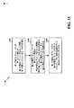
[0057]図11は、レギュレータ回路による方法のフローチャート1100である。方法は、レギュレータ回路(例えば、レギュレータ回路600,650、装置1202/1202’)によって実行され得る。1102において、レギュレータ回路は、第1の電圧レギュレータへの第1の入力電圧を、第1の電圧レギュレータを介して調整し、第1の電圧レギュレータは、PMOSを含む。1104において、レギュレータ回路は、第2の電圧レギュレータへの第2の入力電圧を、第2の電圧レギュレータを介して調整し、第2の電圧レギュレータは、NMOSを含み、ここにおいて、第1の電圧レギュレータは、第2の電圧レギュレータに接続される。1106において、レギュレータ回路は、第1の電圧レギュレータ又は第2の電圧レギュレータのうちの少なくとも1つを、切替え回路を介して選択的にアクティブにする。ある態様では、第1の電圧レギュレータ又は第2の電圧レギュレータのうちの少なくとも1つは、ノイズに基づいて選択的にアクティブにされる。
[0057] FIG. 11 is a
[0058]図12は、例示的な装置1202内の異なるモジュール/手段/構成要素間のデータフローを例示する概念的なデータフロー図1200である。装置は、レギュレータ回路であり得る。装置は、第1の電圧レギュレータモジュール1204と、第2の電圧レギュレータモジュール1206と、切替えモジュール1208とを含む。
[0058] FIG. 12 is a conceptual data flow diagram 1200 that illustrates data flow between different modules / means / components within the
[0059]第1の電圧レギュレータモジュール1204は、第1の電圧レギュレータモジュール1204への第1の入力電圧を調整する。ある態様では、第1の電圧レギュレータモジュール1204は、PMOSを含む。第2の電圧レギュレータモジュール1206は、第2の電圧レギュレータモジュール1206への第2の入力電圧を調整する。ある態様では、第2の電圧レギュレータモジュール1206は、NMOSを含む。ある態様では、第1の電圧レギュレータは、第2の電圧レギュレータに接続される。切替えモジュール1208は、第1の電圧レギュレータモジュール1204及び第2の電圧レギュレータモジュール1206のうちの少なくとも1つを選択的にアクティブにする。ある態様では、第1の電圧レギュレータモジュール1204及び第2の電圧レギュレータ1206うちの少なくとも1つは、ノイズに基づいて選択的にアクティブにされる。
The first
[0060]装置は、上述された図11のフローチャートにおけるアルゴリズムのブロックの各々を実行する追加のモジュールを含み得る。このように、上述された図11のフローチャートにおける各ブロックはモジュールによって実行され得、装置は、これらモジュールのうちの1つ又は複数を含み得る。モジュールは、説明されたプロセス/アルゴリズムを実行するように特に構成されるか、説明されたプロセス/アルゴリズムを行うように構成されたプロセッサによって実装されるか、プロセッサによる実装のためにコンピュータ読取可能な媒体内に格納されるか、又はそれらの何等かの組み合わせである、1つ又は複数のハードウェア構成要素であり得る。 [0060] The apparatus may include additional modules that perform each of the blocks of the algorithm in the flowchart of FIG. 11 described above. Thus, each block in the flowchart of FIG. 11 described above may be performed by a module, and an apparatus may include one or more of these modules. The module is specifically configured to execute the described process / algorithm, implemented by a processor configured to perform the described process / algorithm, or computer readable for implementation by the processor It may be one or more hardware components, stored in a medium or any combination thereof.
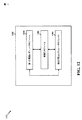
[0061]図13は、処理システム1314を用いる装置1202’のためのハードウェア実装形態の例を例示する図1300である。処理システム1314は、概してバス1324と表されるバスアーキテクチャを用いて実装され得る。バス1324は、処理システム1314の特定の用途と設計制約全体に依存して、任意の数の相互接続バス及びブリッジを含み得る。バス1324は、プロセッサ1304、モジュール1204,1206,1208及びコンピュータ読取可能な媒体/メモリ1306で表される、1つ又は複数のプロセッサ及び/又はハードウェアモジュールを含む様々な回路を互いにリンクさせる。バス1324はまた、タイミングソース、周辺機器、電圧レギュレータ及び電力管理回路のような様々な他の回路をリンクさせ得るが、これらは、当技術分野では周知であるためこれ以上説明されないであろう。
FIG. 13 is a diagram 1300 illustrating an example of a hardware implementation for an
[0062]処理システム1314は、トランシーバ1310に結合され得る。トランシーバ1310は、1つ又は複数のアンテナ1320に結合される。トランシーバ1310は、伝送媒体を通して様々な他の装置と通信するための手段を提供する。トランシーバ1310は、1つ又は複数のアンテナ1320から信号を受け、受けた信号から情報を抽出し、抽出された情報を処理システム1314に提供する。加えて、トランシーバ1310は、処理システム1314から情報を受け、受けた情報に基づいて、1つ又は複数のアンテナ1320に適用される信号を生成する。処理システム1314は、コンピュータ読取可能な媒体/メモリ1306に結合されたプロセッサ1304を含む。プロセッサ1304は、コンピュータ読取可能な媒体/メモリ1306に格納されたソフトウェアの実行を含む、汎用処理を担う。ソフトウェアは、プロセッサ1304によって実行されると、任意の特定の装置に関して先に述べた様々な機能を実行することを処理システム1314に行わせる。コンピュータ読取可能な媒体/メモリ1306はまた、ソフトウェアを実行するときにプロセッサ1304によって操作されるデータを格納するために使用され得る。処理システムは、モジュール1204,1206及び1208のうちの少なくとも1つを更に含む。これらのモジュールは、プロセッサ1304で実行しており、コンピュータ読取可能な媒体/メモリ1306に存在し/格納されたソフトウェアモジュールであるか、プロセッサ1304に結合された1つ又は複数のハードウェアモジュールであるか、又はそれらの何等かの組み合わせであり得る。
[0063]一構成では、装置1202/1202’は、第1の入力電圧を調整するための手段への第1の入力電圧を調整するための手段と、ここで、第1の入力電圧を調整するための手段は、PMOSを含む、第2の電圧を調整するための手段への第2の入力電圧を調整するための手段と、ここで、第2の電圧を調整するための手段は、NMOSを含み、第1の入力電圧を調整するための手段は、第2の電圧を調整するための手段に接続される、第1の入力電圧を調整するための手段又は第2の電圧を制御するための手段のうちの少なくとも1つを選択的にアクティブにするための手段とを含む。ある態様では、選択的にアクティブにするための手段は、第1の入力電圧を調整するための手段及び第2の電圧を調整するための手段のうちの少なくとも1つを、ノイズに基づいて選択的にアクティブにするように構成される。前述の手段は、前述の手段によって説明された機能を実行するように構成された、装置1202の前述のモジュール及び/又は装置1202’の処理システム1314のうちの1つ又は複数であり得る。
[0063] In one configuration, the
[0064]開示されたプロセスにおけるステップの特定の順序又は序列が例示的なアプローチの一例であることは理解されるべきである。設計の選好に基づいて、これらのプロセスにおけるステップの特定の順序又は序列が並べ替えられ得ることは理解される。更に、幾つかのステップは組み合されるか又は省略され得る。添付の方法の請求項は、様々なステップの要素を1つの例示的な順序で示すが、それらが提示された特定の順序又は序列に限定されることは意味されない。 [0064] It should be understood that the specific order or hierarchy of steps in the processes disclosed is an example of exemplary approaches. It is understood that based on design preferences, the particular order or order of steps in these processes may be rearranged. Furthermore, some steps may be combined or omitted. The appended method claims present elements of the various steps in a single illustrative order, and are not meant to be limited to the specific order or hierarchy in which they are presented.
[0065]先の説明は、当業者による、本明細書に説明された様々な態様の実施を可能にするために提供される。これらの態様に対する様々な修正は、当業者には容易に明らかとなり、本明細書において定義された包括的な原理は、他の態様に適用され得る。故に、特許請求の範囲は、本明細書で示された態様に限定されることを意図しておらず、特許請求の範囲の文言と一致する全範囲が付与されるべきものであり、ここにおいて、単数形の要素への参照は、そのように明記されていない限り、「1つ及び1つのみ」を意味することを意図するものではなく、「1つ又は複数」を意味する。別途明記されていない限り、「何等かの/幾つかの」という用語は、1つ又は複数を指す。当業者に知られているか又は後に知られることとなる、本開示全体にわたって説明された様々な態様の要素と構造的及び機能的に同等なものは全て、参照によって本明細書に明確に組み込まれ、そして特許請求の範囲によって包含されることが意図される。更に、本明細書に開示されたものは何れも、そのような開示が特許請求の範囲に明示的に記載されているかどうかに関わらず、公に献呈されることを意図するものではない。何れの請求項の要素も、その要素が「〜ための手段」という表現を使用して明記されていない限り、ミーンズプラスファンクション(means plus function)として解釈されるべきではない。
以下に本願発明の当初の特許請求の範囲に記載された発明を付記する。
[C1]
レギュレータ回路であって、
第1の電圧レギュレータへの第1の入力電圧を調整するための前記第1の電圧レギュレータと、ここで、前記第1の電圧レギュレータは、P型金属酸化膜半導体(PMOS)を含み、
第2の電圧レギュレータへの第2の入力電圧を調整するための前記第2の電圧レギュレータと、ここで、前記第2の電圧レギュレータは、N型金属酸化膜半導体(NMOS)を含み、前記第1の電圧レギュレータは、前記第2の電圧レギュレータに接続され、
前記第1の電圧レギュレータ又は前記第2の電圧レギュレータのうちの少なくとも1つを選択的にアクティブにするための切替え回路と
を備えるレギュレータ回路。
[C2]
前記切替え回路は、前記第1の電圧レギュレータ又は前記第2の電圧レギュレータのうちの少なくとも1つを、ノイズに基づいて選択的にアクティブにする、C1に記載のレギュレータ回路。
[C3]
前記第1の電圧レギュレータ及び前記第2の電圧レギュレータは、直列に接続される、C1に記載のレギュレータ回路。
[C4]
前記第1の電圧レギュレータ及び前記第2の電圧レギュレータは、並列に接続される、C1に記載のレギュレータ回路。
[C5]
前記第1の電圧レギュレータは、2つの段において前記第1の入力電圧を増幅するための二段式増幅器回路を含む、C1に記載のレギュレータ回路。
[C6]
前記第2の電圧レギュレータは、2つの段において前記第2の入力電圧を増幅するための二段式増幅器回路を含む、C1に記載のレギュレータ回路。
[C7]
前記第2の電圧レギュレータは、ポールキャンセレーション回路を含む、C1に記載のレギュレータ回路。
[C8]
前記第2の電圧レギュレータは、キャパシタ及び抵抗器を含み、前記抵抗器の一端は、前記キャパシタに接続され、前記抵抗器の別の端は、前記NMOSのソースに接続される、C1に記載のレギュレータ回路。
[C9]
前記第1の電圧レギュレータ及び前記第2の電圧レギュレータは、入力電圧調整の程度を変更するように調節可能である、C1に記載のレギュレータ回路。
[C10]
前記第1の電圧レギュレータ及び前記第2の電圧レギュレータは、異なる入力インピーダンス及び出力インピーダンスを有する、C1に記載のレギュレータ回路。
[C11]
レギュレータ回路による方法であって、
第1の電圧レギュレータへの第1の入力電圧を、前記第1の電圧レギュレータを介して調整することと、ここで、前記第1の電圧レギュレータは、P型金属酸化膜半導体(PMOS)を含む、
第2の電圧レギュレータへの第2の入力電圧を、前記第2の電圧レギュレータを介して調整することと、ここで、前記第2の電圧レギュレータは、N型金属酸化膜半導体(NMOS)を含み、前記第1の電圧レギュレータは、前記第2の電圧レギュレータに接続され、
前記第1の電圧レギュレータ又は前記第2の電圧レギュレータのうちの少なくとも1つを、切替え回路を介して選択的にアクティブにすることと
を備える方法。
[C12]
前記第1の電圧レギュレータ又は前記第2の電圧レギュレータのうちの前記少なくとも1つは、ノイズに基づいて選択的にアクティブにされる、C11に記載の方法。
[C13]
レギュレータ回路であって、
第1の入力電圧を調整するための手段への前記第1の入力電圧を調整するための前記手段と、ここで、前記第1の入力電圧を調整するための前記手段は、P型金属酸化膜半導体(PMOS)を含み、
第2の電圧を調整するための手段への前記第2の入力電圧を調整するための前記手段と、ここで、前記第2の電圧を調整するための前記手段は、N型金属酸化膜半導体(NMOS)を含み、前記第1の入力電圧を調整するための前記手段は、前記第2の電圧を調整するための前記手段に接続され、
前記第1の入力電圧を調整するための前記手段又は前記第2の電圧を調整するための前記手段のうちの少なくとも1つを選択的にアクティブにするための手段と
を備えるレギュレータ回路。
[C14]
選択的にアクティブにするための前記手段は、前記第1の入力電圧を調整するための前記手段又は前記第2の電圧を調整するための前記手段のうちの少なくとも1つを、ノイズに基づいて選択的にアクティブにするように構成される、C13に記載のレギュレータ回路。
[0065] The previous description is provided to enable any person skilled in the art to practice the various aspects described herein. Various modifications to these aspects will be readily apparent to those skilled in the art, and the generic principles defined herein may be applied to other aspects. Thus, the claims are not intended to be limited to the embodiments set forth herein, but should be given the full scope consistent with the wording of the claims, where Reference to an element in the singular form is not intended to mean "one and only one" unless specifically stated otherwise, and means "one or more". Unless otherwise stated, the term "something / some" refers to one or more. All structural and functional equivalents of the elements of the various embodiments described throughout the present disclosure, which will be known to those skilled in the art or as will be known later, are expressly incorporated herein by reference. And is intended to be encompassed by the following claims. Moreover, nothing disclosed herein is intended to be dedicated publicly, regardless of whether such disclosure is explicitly recited in the claims. Elements of any of the claims should not be construed as means plus function unless the element is specified using the phrase "means for."
The invention described in the original claim of this invention is appended to the following.
[C1]
A regulator circuit,
A first voltage regulator for adjusting a first input voltage to a first voltage regulator, wherein the first voltage regulator includes a P-type metal oxide semiconductor (PMOS);
A second voltage regulator for adjusting a second input voltage to a second voltage regulator, wherein the second voltage regulator includes an N-type metal oxide semiconductor (NMOS); A voltage regulator is connected to the second voltage regulator,
A switching circuit for selectively activating at least one of the first voltage regulator or the second voltage regulator;
Regulator circuit comprising:
[C2]
The regulator circuit according to C1, wherein the switching circuit selectively activates at least one of the first voltage regulator or the second voltage regulator based on noise.
[C3]
The regulator circuit according to C1, wherein the first voltage regulator and the second voltage regulator are connected in series.
[C4]
The regulator circuit according to C1, wherein the first voltage regulator and the second voltage regulator are connected in parallel.
[C5]
The regulator circuit of C1, wherein the first voltage regulator comprises a two-stage amplifier circuit for amplifying the first input voltage in two stages.
[C6]
The regulator circuit according to C1, wherein the second voltage regulator comprises a two-stage amplifier circuit for amplifying the second input voltage in two stages.
[C7]
The regulator circuit of C1, wherein the second voltage regulator comprises a pole cancellation circuit.
[C8]
The second voltage regulator includes a capacitor and a resistor, wherein one end of the resistor is connected to the capacitor, and the other end of the resistor is connected to a source of the NMOS. Regulator circuit.
[C9]
The regulator circuit of C1, wherein the first voltage regulator and the second voltage regulator are adjustable to change the degree of input voltage regulation.
[C10]
The regulator circuit according to C1, wherein the first voltage regulator and the second voltage regulator have different input and output impedances.
[C11]
A method by means of a regulator circuit,
Adjusting a first input voltage to a first voltage regulator via the first voltage regulator, wherein the first voltage regulator includes a P-type metal oxide semiconductor (PMOS) ,
Adjusting a second input voltage to a second voltage regulator via the second voltage regulator, wherein the second voltage regulator includes an N-type metal oxide semiconductor (NMOS) The first voltage regulator is connected to the second voltage regulator,
Selectively activating at least one of the first voltage regulator or the second voltage regulator via a switching circuit;
How to provide.
[C12]
The method of C11, wherein the at least one of the first voltage regulator or the second voltage regulator is selectively activated based on noise.
[C13]
A regulator circuit,
Means for adjusting the first input voltage to the means for adjusting the first input voltage, wherein the means for adjusting the first input voltage is P-type metal oxide Film semiconductor (PMOS),
Means for adjusting the second input voltage to the means for adjusting a second voltage, wherein the means for adjusting the second voltage comprises an N-type metal oxide semiconductor The means for adjusting the first input voltage, including (NMOS), connected to the means for adjusting the second voltage,
Means for selectively activating at least one of the means for adjusting the first input voltage or the means for adjusting the second voltage
Regulator circuit comprising:
[C14]
The means for selectively activating comprises noise based at least one of the means for adjusting the first input voltage or the means for adjusting the second voltage. The regulator circuit according to C13, configured to selectively activate.
Claims (9)
第1の電圧レギュレータへの第1の入力電圧を調整するための前記第1の電圧レギュレータと、ここで、前記第1の電圧レギュレータは、P型金属酸化膜半導体(PMOS)パス素子を含み、
第2の電圧レギュレータへの第2の入力電圧を調整するための前記第2の電圧レギュレータと、ここで、前記第2の電圧レギュレータは、N型金属酸化膜半導体(NMOS)パス素子を含み、前記第1の電圧レギュレータは、前記第2の電圧レギュレータに接続される、
を備え、
電圧モードを選択し、選択された前記電圧モードに基づいて、前記第1の電圧レギュレータ又は前記第2の電圧レギュレータのうちの少なくとも1つを選択的にアクティブにするための切替え回路
をさらに備えることを特徴とし、
前記切替え回路は、前記VCOレギュレータ回路に接続されたVCOの影響に基づいて前記電圧モードを選択するように、及び、前記影響に基づいて前記第1の電圧レギュレータ又は前記第2の電圧レギュレータのうちの前記少なくとも1つを選択的にアクティブにするように構成される、レギュレータ回路。 A voltage controlled oscillator (VCO) regulator circuit,
A first voltage regulator for adjusting a first input voltage to a first voltage regulator, wherein the first voltage regulator includes a P-type metal oxide semiconductor (PMOS) pass element ;
A second voltage regulator for adjusting a second input voltage to a second voltage regulator, wherein the second voltage regulator includes an N-type metal oxide semiconductor (NMOS) pass element ; the first voltage regulator, Ru is connected to the second voltage regulator,
Equipped with
It selects the voltage mode, based on the voltage mode is selected, further comprising a switching circuitry for selectively activating at least one of said first voltage regulator and the second voltage regulator It is characterized by
The switching circuit is configured to select the voltage mode based on an influence of a VCO connected to the VCO regulator circuit, and among the first voltage regulator or the second voltage regulator based on the influence. A regulator circuit configured to selectively activate said at least one of
第1の電圧レギュレータへの第1の入力電圧を、前記第1の電圧レギュレータを介して調整することと、ここで、前記第1の電圧レギュレータは、P型金属酸化膜半導体(PMOS)パス素子を含む、
第2の電圧レギュレータへの第2の入力電圧を、前記第2の電圧レギュレータを介して調整することと、ここで、前記第2の電圧レギュレータは、N型金属酸化膜半導体(NMOS)素子を含み、前記第1の電圧レギュレータは、前記第2の電圧レギュレータに接続される、
を備え、
選択された電圧モードに基づいて、前記第1の電圧レギュレータ又は前記第2の電圧レギュレータのうちの少なくとも1つを選択的にアクティブにするために、切替え回路を介して、前記電圧モードを選択すること
をさらに備えることを特徴とし、
前記電圧モードは、前記VCOレギュレータ回路に接続されたVCOの影響に基づいて、及び、前記影響に基づいて前記第1の電圧レギュレータ又は前記第2の電圧レギュレータのうちの前記少なくとも1つを選択的にアクティブにために、選択される、
方法。 Method by voltage controlled oscillator (VCO) regulator circuit, wherein
Adjusting a first input voltage to a first voltage regulator via the first voltage regulator, wherein the first voltage regulator is a P-type metal oxide semiconductor (PMOS) pass element including,
Adjusting a second input voltage to a second voltage regulator via the second voltage regulator, wherein the second voltage regulator comprises an N-type metal oxide semiconductor (NMOS) device ; wherein, the first voltage regulator, Ru is connected to the second voltage regulator,
Equipped with
Based on the voltage mode is selected, in order to activate the at least one channel selection択的of said first voltage regulator and the second voltage regulator, through the switching circuit, selects the voltage mode and further comprising a call for,
The voltage mode is selectively based on the effect of a VCO connected to the VCO regulator circuit and based on the effect selectively the at least one of the first voltage regulator or the second voltage regulator. Selected to be active on
Method.
Applications Claiming Priority (5)
| Application Number | Priority Date | Filing Date | Title |
|---|---|---|---|
| US201462005765P | 2014-05-30 | 2014-05-30 | |
| US62/005,765 | 2014-05-30 | ||
| US14/630,506 US11095216B2 (en) | 2014-05-30 | 2015-02-24 | On-chip dual-supply multi-mode CMOS regulators |
| US14/630,506 | 2015-02-24 | ||
| PCT/US2015/030948 WO2015183588A1 (en) | 2014-05-30 | 2015-05-15 | On-chip dual-supply multi-mode cmos regulators |
Publications (3)
| Publication Number | Publication Date |
|---|---|
| JP2017517073A JP2017517073A (en) | 2017-06-22 |
| JP2017517073A5 JP2017517073A5 (en) | 2018-06-07 |
| JP6522666B2 true JP6522666B2 (en) | 2019-05-29 |
Family
ID=53284554
Family Applications (1)
| Application Number | Title | Priority Date | Filing Date |
|---|---|---|---|
| JP2016569919A Active JP6522666B2 (en) | 2014-05-30 | 2015-05-15 | On-Chip Dual-Supply Multi-Mode CMOS Regulator |
Country Status (7)
| Country | Link |
|---|---|
| US (2) | US11095216B2 (en) |
| EP (2) | EP3149553B1 (en) |
| JP (1) | JP6522666B2 (en) |
| KR (1) | KR20170013248A (en) |
| CN (1) | CN106462175B (en) |
| BR (1) | BR112016028170A2 (en) |
| WO (1) | WO2015183588A1 (en) |
Families Citing this family (13)
| Publication number | Priority date | Publication date | Assignee | Title |
|---|---|---|---|---|
| US11095216B2 (en) * | 2014-05-30 | 2021-08-17 | Qualcomm Incorporated | On-chip dual-supply multi-mode CMOS regulators |
| US9588541B1 (en) | 2015-10-30 | 2017-03-07 | Qualcomm Incorporated | Dual loop regulator circuit |
| US9946283B1 (en) | 2016-10-18 | 2018-04-17 | Qualcomm Incorporated | Fast transient response low-dropout (LDO) regulator |
| US10411599B1 (en) | 2018-03-28 | 2019-09-10 | Qualcomm Incorporated | Boost and LDO hybrid converter with dual-loop control |
| US10444780B1 (en) | 2018-09-20 | 2019-10-15 | Qualcomm Incorporated | Regulation/bypass automation for LDO with multiple supply voltages |
| US10591938B1 (en) | 2018-10-16 | 2020-03-17 | Qualcomm Incorporated | PMOS-output LDO with full spectrum PSR |
| US10545523B1 (en) | 2018-10-25 | 2020-01-28 | Qualcomm Incorporated | Adaptive gate-biased field effect transistor for low-dropout regulator |
| KR20200145968A (en) | 2019-06-21 | 2020-12-31 | 삼성전자주식회사 | Electronic circuit for configuring amplifying circuit configured to output voltage including low noise |
| US11372436B2 (en) | 2019-10-14 | 2022-06-28 | Qualcomm Incorporated | Simultaneous low quiescent current and high performance LDO using single input stage and multiple output stages |
| US11429129B2 (en) * | 2020-05-13 | 2022-08-30 | Sensata Technologies, Inc. | Multi-deck circuits with common rails |
| US11280847B1 (en) * | 2020-10-30 | 2022-03-22 | Taiwan Semiconductor Manufacturing Company Ltd. | Circuit, semiconductor device and method for parameter PSRR measurement |
| US11803204B2 (en) * | 2021-04-23 | 2023-10-31 | Qualcomm Incorporated | Low-dropout (LDO) voltage regulator with voltage droop compensation circuit |
| KR20220169850A (en) * | 2021-06-21 | 2022-12-28 | 에스케이하이닉스 주식회사 | Electronic device performing a power switching operation |
Family Cites Families (59)
| Publication number | Priority date | Publication date | Assignee | Title |
|---|---|---|---|---|
| US5336986A (en) * | 1992-02-07 | 1994-08-09 | Crosspoint Solutions, Inc. | Voltage regulator for field programmable gate arrays |
| JP2839819B2 (en) * | 1993-05-28 | 1998-12-16 | 株式会社東芝 | Nonvolatile semiconductor memory device |
| US5528127A (en) | 1994-05-17 | 1996-06-18 | National Semiconductor Corporation | Controlling power dissipation within a linear voltage regulator circuit |
| JP2001159921A (en) | 1999-12-03 | 2001-06-12 | Seiko Epson Corp | Power supply circuit |
| JP2001282371A (en) | 2000-03-31 | 2001-10-12 | Seiko Instruments Inc | Voltage regulator |
| US6515880B1 (en) * | 2001-10-19 | 2003-02-04 | Texas Instruments Incorporated | Soft-start control for DC/DC switching regulators |
| US6677735B2 (en) | 2001-12-18 | 2004-01-13 | Texas Instruments Incorporated | Low drop-out voltage regulator having split power device |
| DE10215084A1 (en) | 2002-04-05 | 2003-10-30 | Infineon Technologies Ag | Circuit arrangement for voltage regulation |
| EP1437638B1 (en) | 2002-12-17 | 2016-02-24 | Infineon Technologies AG | Circuit for generating a voltage supply |
| DE10334066A1 (en) | 2003-07-25 | 2005-02-24 | Infineon Technologies Ag | Circuit arrangement for voltage regulation and method for operating a Schaltunsanordnung for Spannugsregelung |
| US7161339B2 (en) | 2003-08-20 | 2007-01-09 | Broadcom Corporation | High voltage power management unit architecture in CMOS process |
| US6879142B2 (en) | 2003-08-20 | 2005-04-12 | Broadcom Corporation | Power management unit for use in portable applications |
| US6894472B2 (en) | 2003-08-20 | 2005-05-17 | Broadcom Corporation | Low leakage CMOS power mux |
| US7145370B2 (en) * | 2003-09-05 | 2006-12-05 | Impinj, Inc. | High-voltage switches in single-well CMOS processes |
| US7177182B2 (en) * | 2004-03-30 | 2007-02-13 | Impinj, Inc. | Rewriteable electronic fuses |
| US6979983B2 (en) | 2004-04-28 | 2005-12-27 | Faraday Technology Corp. | Voltage regulator |
| US7268993B2 (en) | 2004-05-25 | 2007-09-11 | Sbc Knowledge Ventures, L.P. | Integrated protector and splitter |
| JP4396402B2 (en) * | 2004-06-03 | 2010-01-13 | ソニー株式会社 | Constant voltage power circuit |
| WO2006027831A1 (en) * | 2004-09-08 | 2006-03-16 | Fujitsu Limited | Pll frequency synthesizer |
| EP1669831A1 (en) | 2004-12-03 | 2006-06-14 | Dialog Semiconductor GmbH | Voltage regulator output stage with low voltage MOS devices |
| US7071664B1 (en) | 2004-12-20 | 2006-07-04 | Texas Instruments Incorporated | Programmable voltage regulator configurable for double power density and reverse blocking |
| US7106032B2 (en) | 2005-02-03 | 2006-09-12 | Aimtron Technology Corp. | Linear voltage regulator with selectable light and heavy load paths |
| US7064531B1 (en) | 2005-03-31 | 2006-06-20 | Micrel, Inc. | PWM buck regulator with LDO standby mode |
| US7253663B2 (en) | 2005-06-15 | 2007-08-07 | Ati Technologies Inc. | Apparatus and methods for self-biasing differential signaling circuitry having multimode output configurations for low voltage applications |
| US20070002596A1 (en) | 2005-06-29 | 2007-01-04 | Eaton Corporation | Two-stage, wide range power supply for a network protector control relay |
| JP4774247B2 (en) | 2005-07-21 | 2011-09-14 | Okiセミコンダクタ株式会社 | Voltage regulator |
| US7199565B1 (en) | 2006-04-18 | 2007-04-03 | Atmel Corporation | Low-dropout voltage regulator with a voltage slew rate efficient transient response boost circuit |
| US7531996B2 (en) | 2006-11-21 | 2009-05-12 | System General Corp. | Low dropout regulator with wide input voltage range |
| US7583116B2 (en) * | 2007-08-03 | 2009-09-01 | International Business Machines Corporation | High output resistance, wide swing charge pump |
| US7548093B1 (en) | 2008-03-05 | 2009-06-16 | Freescale Semiconductor, Inc. | Scheme of level shifter cell |
| TWI355801B (en) | 2008-04-01 | 2012-01-01 | Richtek Technology Corp | Dual power switch and voltage regulator using same |
| US7952900B2 (en) * | 2008-04-16 | 2011-05-31 | Analog Devices, Inc. | H-bridge buck-boost converter |
| US7863878B2 (en) | 2008-08-19 | 2011-01-04 | Oracle America, Inc. | Voltage regulator for write/read assist circuit |
| US8305056B2 (en) * | 2008-12-09 | 2012-11-06 | Qualcomm Incorporated | Low drop-out voltage regulator with wide bandwidth power supply rejection ratio |
| US7994759B2 (en) | 2009-04-13 | 2011-08-09 | Himax Technologies Limited | System and method for driving a power supply device in an initial activation stage |
| JP2010252094A (en) * | 2009-04-16 | 2010-11-04 | Renesas Electronics Corp | Pll circuit |
| US7961056B2 (en) | 2009-09-10 | 2011-06-14 | Intel Corporation | Low phase noise voltage controlled oscillator |
| EP2354881A1 (en) | 2010-02-05 | 2011-08-10 | Dialog Semiconductor GmbH | Domino voltage regulator (DVR) |
| WO2011099965A1 (en) | 2010-02-10 | 2011-08-18 | Skyworks Solutions, Inc. | Multi-mode power supply regulator for power amplifier control |
| US8774739B2 (en) * | 2010-02-10 | 2014-07-08 | Skyworks Solutions, Inc. | Multi-mode power supply regulator for power amplifier control |
| US8519771B1 (en) | 2010-12-22 | 2013-08-27 | Xilinx, Inc. | Methods and apparatus for receiving high and low voltage signals using a low supply voltage technology |
| CN102096434B (en) * | 2010-12-23 | 2012-11-28 | 东南大学 | High-slew-rate error amplifier-based high-accuracy and high-speed low dropout (LDO) regulator circuit |
| US8373446B2 (en) * | 2010-12-28 | 2013-02-12 | Texas Instruments Incorporated | Power supply detection circuit |
| JP2012147648A (en) | 2011-01-14 | 2012-08-02 | Sony Corp | Power control device and power control method |
| WO2013009418A1 (en) | 2011-07-08 | 2013-01-17 | Rambus Inc. | High-speed low-power stacked transceiver |
| CN102354245B (en) | 2011-08-05 | 2013-06-12 | 电子科技大学 | Band gap voltage reference source |
| US8476940B2 (en) | 2011-12-02 | 2013-07-02 | Stmicroelectronics International N.V. | Stress reduced cascoded CMOS output driver circuit |
| US20130169246A1 (en) | 2011-12-28 | 2013-07-04 | Skymedi Corporation | Linear voltage regulating circuit adaptable to a logic system |
| CN102609023B (en) | 2012-03-12 | 2013-11-20 | 北京经纬恒润科技有限公司 | Built-in analog power supply circuit |
| US8890610B2 (en) * | 2012-03-28 | 2014-11-18 | Texas Instruments Incorporated | Compensation circuitry and method for amplifiers driving large capacitive loads |
| JP6004836B2 (en) * | 2012-08-22 | 2016-10-12 | ルネサスエレクトロニクス株式会社 | Power supply device, semiconductor device, and wireless communication device |
| US8981739B2 (en) * | 2012-09-26 | 2015-03-17 | Nxp B.V. | Low power low dropout linear voltage regulator |
| JP6211822B2 (en) * | 2012-09-28 | 2017-10-11 | 旭化成エレクトロニクス株式会社 | Power supply circuit |
| US9170590B2 (en) | 2012-10-31 | 2015-10-27 | Qualcomm Incorporated | Method and apparatus for load adaptive LDO bias and compensation |
| US9235225B2 (en) | 2012-11-06 | 2016-01-12 | Qualcomm Incorporated | Method and apparatus reduced switch-on rate low dropout regulator (LDO) bias and compensation |
| US8890499B2 (en) | 2013-03-11 | 2014-11-18 | Micrel, Inc. | Buck DC-DC converter with improved accuracy |
| CN103647449B (en) | 2013-12-18 | 2016-08-17 | 嘉兴中润微电子有限公司 | A kind of boost-type charge pump circuit |
| US9231525B2 (en) * | 2014-02-28 | 2016-01-05 | Google Inc. | Compensating a two stage amplifier |
| US11095216B2 (en) * | 2014-05-30 | 2021-08-17 | Qualcomm Incorporated | On-chip dual-supply multi-mode CMOS regulators |
-
2015
- 2015-02-24 US US14/630,506 patent/US11095216B2/en active Active
- 2015-05-15 CN CN201580028351.6A patent/CN106462175B/en active Active
- 2015-05-15 EP EP15727151.1A patent/EP3149553B1/en active Active
- 2015-05-15 KR KR1020167033178A patent/KR20170013248A/en unknown
- 2015-05-15 BR BR112016028170A patent/BR112016028170A2/en not_active Application Discontinuation
- 2015-05-15 EP EP22197509.7A patent/EP4130925A1/en active Pending
- 2015-05-15 JP JP2016569919A patent/JP6522666B2/en active Active
- 2015-05-15 WO PCT/US2015/030948 patent/WO2015183588A1/en active Application Filing
-
2021
- 2021-07-20 US US17/443,093 patent/US11726513B2/en active Active
Also Published As
| Publication number | Publication date |
|---|---|
| EP3149553A1 (en) | 2017-04-05 |
| WO2015183588A1 (en) | 2015-12-03 |
| US20150349622A1 (en) | 2015-12-03 |
| JP2017517073A (en) | 2017-06-22 |
| US20210351696A1 (en) | 2021-11-11 |
| US11095216B2 (en) | 2021-08-17 |
| EP4130925A1 (en) | 2023-02-08 |
| BR112016028170A2 (en) | 2017-08-22 |
| CN106462175B (en) | 2018-03-16 |
| EP3149553B1 (en) | 2022-11-23 |
| CN106462175A (en) | 2017-02-22 |
| KR20170013248A (en) | 2017-02-06 |
| US11726513B2 (en) | 2023-08-15 |
Similar Documents
| Publication | Publication Date | Title |
|---|---|---|
| JP6522666B2 (en) | On-Chip Dual-Supply Multi-Mode CMOS Regulator | |
| CN107078693B (en) | Circuit for providing harmonic response suppression for mixer | |
| US9106234B2 (en) | Programmable frequency divider for local oscillator generation | |
| JP6328862B1 (en) | Ring oscillator architecture with controlled sensitivity to supply voltage | |
| US8988158B2 (en) | Hybrid voltage controlled oscillator | |
| JP2018532295A (en) | Low noise amplifier and notch filter | |
| JP6625564B2 (en) | Differential mode bandwidth extension technique using common mode compensation | |
| JP2018504020A (en) | Apparatus and method for generating a quadruple reference clock from a single-ended crystal oscillator | |
| US9608569B2 (en) | Linearizing scheme for baseband filter with active feedback | |
| US20160099729A1 (en) | Apparatus and method for quadrupling frequency of reference clock | |
| US9209771B1 (en) | EM coupling shielding |
Legal Events
| Date | Code | Title | Description |
|---|---|---|---|
| A521 | Request for written amendment filed |
Free format text: JAPANESE INTERMEDIATE CODE: A523 Effective date: 20180420 |
|
| A621 | Written request for application examination |
Free format text: JAPANESE INTERMEDIATE CODE: A621 Effective date: 20180420 |
|
| A977 | Report on retrieval |
Free format text: JAPANESE INTERMEDIATE CODE: A971007 Effective date: 20190320 |
|
| TRDD | Decision of grant or rejection written | ||
| A01 | Written decision to grant a patent or to grant a registration (utility model) |
Free format text: JAPANESE INTERMEDIATE CODE: A01 Effective date: 20190402 |
|
| A61 | First payment of annual fees (during grant procedure) |
Free format text: JAPANESE INTERMEDIATE CODE: A61 Effective date: 20190424 |
|
| R150 | Certificate of patent or registration of utility model |
Ref document number: 6522666 Country of ref document: JP Free format text: JAPANESE INTERMEDIATE CODE: R150 |
|
| R250 | Receipt of annual fees |
Free format text: JAPANESE INTERMEDIATE CODE: R250 |
|
| R250 | Receipt of annual fees |
Free format text: JAPANESE INTERMEDIATE CODE: R250 |