KR20170013248A - On-chip dual-supply multi-mode cmos regulators - Google Patents
On-chip dual-supply multi-mode cmos regulators Download PDFInfo
- Publication number
- KR20170013248A KR20170013248A KR1020167033178A KR20167033178A KR20170013248A KR 20170013248 A KR20170013248 A KR 20170013248A KR 1020167033178 A KR1020167033178 A KR 1020167033178A KR 20167033178 A KR20167033178 A KR 20167033178A KR 20170013248 A KR20170013248 A KR 20170013248A
- Authority
- KR
- South Korea
- Prior art keywords
- regulator
- voltage
- circuit
- voltage regulator
- regulating
- Prior art date
Links
Images


Classifications
-
- H—ELECTRICITY
- H02—GENERATION; CONVERSION OR DISTRIBUTION OF ELECTRIC POWER
- H02M—APPARATUS FOR CONVERSION BETWEEN AC AND AC, BETWEEN AC AND DC, OR BETWEEN DC AND DC, AND FOR USE WITH MAINS OR SIMILAR POWER SUPPLY SYSTEMS; CONVERSION OF DC OR AC INPUT POWER INTO SURGE OUTPUT POWER; CONTROL OR REGULATION THEREOF
- H02M3/00—Conversion of dc power input into dc power output
- H02M3/02—Conversion of dc power input into dc power output without intermediate conversion into ac
- H02M3/04—Conversion of dc power input into dc power output without intermediate conversion into ac by static converters
- H02M3/10—Conversion of dc power input into dc power output without intermediate conversion into ac by static converters using discharge tubes with control electrode or semiconductor devices with control electrode
- H02M3/145—Conversion of dc power input into dc power output without intermediate conversion into ac by static converters using discharge tubes with control electrode or semiconductor devices with control electrode using devices of a triode or transistor type requiring continuous application of a control signal
- H02M3/155—Conversion of dc power input into dc power output without intermediate conversion into ac by static converters using discharge tubes with control electrode or semiconductor devices with control electrode using devices of a triode or transistor type requiring continuous application of a control signal using semiconductor devices only
- H02M3/156—Conversion of dc power input into dc power output without intermediate conversion into ac by static converters using discharge tubes with control electrode or semiconductor devices with control electrode using devices of a triode or transistor type requiring continuous application of a control signal using semiconductor devices only with automatic control of output voltage or current, e.g. switching regulators
-
- G—PHYSICS
- G05—CONTROLLING; REGULATING
- G05F—SYSTEMS FOR REGULATING ELECTRIC OR MAGNETIC VARIABLES
- G05F1/00—Automatic systems in which deviations of an electric quantity from one or more predetermined values are detected at the output of the system and fed back to a device within the system to restore the detected quantity to its predetermined value or values, i.e. retroactive systems
- G05F1/10—Regulating voltage or current
- G05F1/46—Regulating voltage or current wherein the variable actually regulated by the final control device is dc
- G05F1/56—Regulating voltage or current wherein the variable actually regulated by the final control device is dc using semiconductor devices in series with the load as final control devices
- G05F1/575—Regulating voltage or current wherein the variable actually regulated by the final control device is dc using semiconductor devices in series with the load as final control devices characterised by the feedback circuit
-
- H—ELECTRICITY
- H02—GENERATION; CONVERSION OR DISTRIBUTION OF ELECTRIC POWER
- H02M—APPARATUS FOR CONVERSION BETWEEN AC AND AC, BETWEEN AC AND DC, OR BETWEEN DC AND DC, AND FOR USE WITH MAINS OR SIMILAR POWER SUPPLY SYSTEMS; CONVERSION OF DC OR AC INPUT POWER INTO SURGE OUTPUT POWER; CONTROL OR REGULATION THEREOF
- H02M1/00—Details of apparatus for conversion
- H02M1/0067—Converter structures employing plural converter units, other than for parallel operation of the units on a single load
- H02M1/0077—Plural converter units whose outputs are connected in series
-
- H02M2001/0077—
Abstract
방법, 장치 및 컴퓨터 프로그램 제품이 제공된다. 장치는 레귤레이터 회로일 수 있다. 레귤레이터 회로는 제 1 전압 레귤레이터에 대한 제 1 입력 전압을 레귤레이팅하는 제 1 전압 레귤레이터 ― 상기 제 1 전압 레귤레이터는 P-타입 금속-산화물-반도체(PMOS)를 포함함 ― ; 및 제 2 전압 레귤레이터에 대한 제 2 입력 전압을 레귤레이팅하는 제 2 전압 레귤레이터를 포함하며, 상기 제 2 전압 레귤레이터는 N-타입 금속-산화물-반도체(NMOS)를 포함한다. 일 양상에서, 제 1 전압 레귤레이터는 제 2 전압 레귤레이터에 커플링된다. A method, apparatus and computer program product are provided. The device may be a regulator circuit. A regulator circuit includes a first voltage regulator that regulates a first input voltage to a first voltage regulator, the first voltage regulator includes a P-type metal-oxide-semiconductor (PMOS); And a second voltage regulator for regulating a second input voltage to the second voltage regulator, wherein the second voltage regulator includes an N-type metal-oxide-semiconductor (NMOS). In an aspect, the first voltage regulator is coupled to the second voltage regulator.
Description
관련 출원들에 대한 교차-참조Cross-reference to related applications
[0001] 본 출원은 2014년 5월 30일 출원되고 발명의 명칭이 “ON-CHIP DUAL-SUPPLY MULTI-MODE CMOS REGULATORS”인 미국 가출원 일련 번호 제62/005,765호 및 2015년 2월 24일 출원되고 발명이 명칭이 "ON-CHIP DUAL-SUPPLY MULTI-MODE CMOS REGULATORS"인 미국 특허 출원 번호 제14/630,506호를 우선권으로 주장하며, 이들은 그 전체가 인용에 의해 본원에 명시적으로 포함된다. [0001] This application claims the benefit of U.S. Provisional Application Serial No. 62 / 005,765 filed on May 30, 2014 entitled " ON-CHIP DUAL-SUPPLY MULTI-MODE CMOS REGULATORS ", filed February 24, 2015, U.S. Patent Application Serial No. 14 / 630,506, entitled " ON-CHIP DUAL-SUPPLY MULTI-MODE CMOS REGULATORS ", which is expressly incorporated herein by reference in its entirety.
분야Field
[0002] 본 개시는 일반적으로 통신 시스템들에 관한 것으로서, 보다 상세하게는, 전압 제어 오실레이터(VCO)에 대한 전압 레귤레이터에 관한 것이다. [0002] [0001] This disclosure relates generally to communication systems, and more particularly, to a voltage regulator for a voltage controlled oscillator (VCO).
[0003] 무선 디바이스(예를 들어, 셀룰러 폰 또는 스마트 폰)은 무선 통신 시스템과의 양방향 통신을 위해 데이터를 송신 및 수신할 수 있다. 무선 디바이스는 데이터 송신을 위한 송신기 및 데이터 수신을 위한 수신기를 포함할 수 있다. 데이터 송신을 위해, 송신기는 데이터로 로컬 오실레이터(LO) 신호를 변조하여 변조된 라디오 주파수(RF) 신호를 획득하고, 변조된 RF 신호를 증폭하여 원하는 출력 전력 레벨을 갖는 출력 RF 신호를 획득하고, 안테나를 통해 기지국에 출력 RF 신호를 송신할 수 있다. 데이터 수신을 위해, 수신기는 안테나를 통해 수신된 RF 신호를 획득하고, 수신된 LO 신호로 수신된 RF 신호를 증폭 및 하향변환하고, 하향변환된 신호를 프로세싱하여 기지국에 의해 송신된 데이터를 복원할 수 있다. [0003] A wireless device (e.g., a cellular phone or smartphone) can transmit and receive data for two-way communication with a wireless communication system. The wireless device may include a transmitter for data transmission and a receiver for data reception. For data transmission, the transmitter modulates the local oscillator (LO) signal with data to obtain a modulated radio frequency (RF) signal, amplifies the modulated RF signal to obtain an output RF signal having a desired output power level, It is possible to transmit the output RF signal to the base station via the antenna. For data reception, the receiver acquires the RF signal received via the antenna, amplifies and downconverts the received RF signal with the received LO signal, and processes the down-converted signal to recover the data transmitted by the base station .
[0004] 무선 디바이스는 하나 또는 그 초과의 원하는 주파수들에서 하나 또는 그 초과의 오실레이터 신호들을 생성하기 위해 하나 또는 그 초과의 오실레이터들을 포함할 수 있다. 오실레이터 신호(들)는 송신기에 대한 송신 LO 신호 및 수신기에 대한 수신 LO 신호를 생성하는데 사용될 수 있다. 오실레이터(들)는 무선 디바이스가 통신하는 무선 통신 시스템의 요건들을 충족시키기 위해 오실레이터 신호(들)를 생성하도록 요구될 수 있다. [0004] A wireless device may include one or more oscillators to produce one or more oscillator signals at one or more desired frequencies. The oscillator signal (s) may be used to generate a transmit LO signal for the transmitter and a receive LO signal for the receiver. The oscillator (s) may be required to generate the oscillator signal (s) to meet the requirements of the wireless communication system with which the wireless device communicates.
[0005] VCO는 송신 LO 신호 및 수신 LO 신호를 생성하는데 사용된다. VCO는 일반적으로 VCO에 입력 전압을 제공하는 레귤레이터에 연결된다. VCO의 성능은 레귤레이터에 의존한다. 따라서, VCO에 대한 효과적인 레귤레이터가 최적의 성능과 낮은 노이즈를 위해 요구된다. [0005] The VCO is used to generate a transmit LO signal and a receive LO signal. The VCO is typically connected to a regulator that provides the input voltage to the VCO. The performance of the VCO depends on the regulator. Thus, an effective regulator for the VCO is required for optimum performance and low noise.
[0006] 본 발명의 일 양상에서, 방법 및 장치가 제공된다. 장치는 레귤레이터 회로일 수 있다. 레귤레이터 회로는 제 1 전압 레귤레이터에 대한 제 1 입력 전압을 레귤레이팅하는 제 1 전압 레귤레이터 ― 제 1 전압 레귤레이터는 P-타입 금속-산화물-반도체(PMOS)를 포함함 ― ; 및 제 2 전압 레귤레이터에 대한 제 2 입력 전압을 레귤레이팅하는 제 2 전압 레귤레이터를 포함하며, 제 2 전압 레귤레이터는 N-타입 금속-산화물-반도체(NMOS)를 포함한다. 일 양상에서, 제 1 전압 레귤레이터는 제 2 전압 레귤레이터에 커플링된다. 일 양상에서, 레귤레이터 회로는 추가로, 제 1 전압 레귤레이터 또는 제 2 전압 레귤레이터 중 적어도 하나를 선택적으로 활성화하는 스위치 회로를 포함할 수 있다. 일 양상에서, 제 1 전압 레귤레이터 및 제 2 전압 레귤레이터는 직렬로 연결된다. 일 양상에서, 제 1 전압 레귤레이터 및 제 2 전압 레귤레이터는 병렬로 연결된다. 일 양상에서, 제 1 전압 레귤레이터는 제 1 입력 전압을 2개의 스테이지들에서 증폭하기 위한 2-스테이지 증폭 회로를 포함한다. 일 양상에서, 제 2 전압 레귤레이터 회로는 제 2 입력 전압을 2개의 스테이지들에서 증폭하기 위한 2-스테이지 증폭 회로를 포함한다. 일 양상에서, 제 2 전압 레귤레이터는 극-소거 회로(pole-cancelation circuit)를 포함한다. 일 양상에서, 제 2 전압 레귤레이터는 커패시터 및 레지스터를 포함하고, 레지스터의 일 단부는 커패시터에 연결되고, 레지스터의 다른 단부는 NMOS의 소스에 연결된다. 일 양상에서, 제 1 전압 레귤레이터 및 제 2 전압 레귤레이터는 입력 전압 레귤레이션의 정도를 변경하도록 튜닝 가능하다. [0006] In one aspect of the invention, a method and apparatus are provided. The device may be a regulator circuit. A regulator circuit includes a first voltage regulator that regulates a first input voltage to a first voltage regulator, the first voltage regulator includes a P-type metal-oxide-semiconductor (PMOS); And a second voltage regulator for regulating a second input voltage to the second voltage regulator, wherein the second voltage regulator includes an N-type metal-oxide-semiconductor (NMOS). In an aspect, the first voltage regulator is coupled to the second voltage regulator. In an aspect, the regulator circuit may further include a switch circuit for selectively activating at least one of the first voltage regulator or the second voltage regulator. In an aspect, the first voltage regulator and the second voltage regulator are connected in series. In an aspect, the first voltage regulator and the second voltage regulator are connected in parallel. In an aspect, the first voltage regulator includes a two-stage amplification circuit for amplifying the first input voltage in two stages. In an aspect, the second voltage regulator circuit includes a two-stage amplification circuit for amplifying the second input voltage in two stages. In an aspect, the second voltage regulator includes a pole-cancelation circuit. In an aspect, the second voltage regulator includes a capacitor and a resistor, one end of the resistor is connected to the capacitor, and the other end of the resistor is connected to the source of the NMOS. In an aspect, the first voltage regulator and the second voltage regulator are tunable to change the degree of input voltage regulation.
[0007]
도 1은 상이한 무선 통신 시스템들과 통신하는 무선 디바이스를 예시한다.
[0008]
도 2는 무선 디바이스의 블록도이다.
[0009]
도 3은 본 개시에 따른 NMOS 레귤레이터의 예시적인 회로도이다.
[0010]
도 4a는 레귤레이터의 다양한 경우에서의 PSSR 값들의 예시적인 PSSR 플롯이다.
[0011]
도 4b는 다양한 경우에서의 노이즈 값들의 예시적인 노이즈 플롯이다.
[0012]
도 5는 본 개시에 따른 NMOS 레귤레이터의 예시적인 구현 회로이다.
[0013]
도 6a 및 도 6b는 CMOS 레귤레이터의 예시적인 구조들이다.
[0014]
도 7은 캐스코드 CMOS 레귤레이터를 포함하는 예시적인 회로도이다.
[0015]
도 8은 버퍼 회로를 포함하는 예시적인 회로도이다.
[0016]
도 9는 본 개시에 따른 시스템 레벨에서의 예시적인 회로 구조이다.
[0017]
도 10a는 VCO의 다양한 경우에서의 PSSR 값들의 예시적인 PSSR 플롯이다.
[0018]
도 10b는 VCO의 다양한 경우에서의 노이즈 값들의 예시적인 노이즈 플롯이다.
[0019]
도 11은 레귤레이터 회로에 의한 방법의 흐름도이다.
[0020]
도 12는 예시적인 장치 내의 상이한 모듈들/수단/컴포넌트들 사이의 데이터 흐름을 예시하는 개념적 데이터 흐름도이다.
[0021]
도 13은 프로세싱 시스템을 이용하는 장치에 대한 하드웨어 구현 예를 예시하는 도면이다. [0007] FIG. 1 illustrates a wireless device that communicates with different wireless communication systems.
[0008] Figure 2 is a block diagram of a wireless device.
[0009] FIG. 3 is an exemplary circuit diagram of an NMOS regulator in accordance with the present disclosure.
[0010] FIG. 4A is an exemplary PSSR plot of PSSR values in various cases of a regulator.
[0011] FIG. 4B is an exemplary noise plot of noise values in various cases.
[0012] FIG. 5 is an exemplary implementation of an NMOS regulator in accordance with the present disclosure;
[0013] FIGS. 6A and 6B are exemplary structures of a CMOS regulator.
[0014] FIG. 7 is an exemplary circuit diagram including a cascode CMOS regulator.
[0015] FIG. 8 is an exemplary circuit diagram including a buffer circuit.
[0016] FIG. 9 is an exemplary circuit architecture at the system level in accordance with the present disclosure.
[0017] FIG. 10A is an exemplary PSSR plot of PSSR values in various cases of a VCO.
[0018] FIG. 10B is an exemplary noise plot of noise values in various cases of a VCO.
[0019] FIG. 11 is a flowchart of a method using a regulator circuit.
[0020] FIG. 12 is a conceptual data flow diagram illustrating the flow of data between different modules / means / components within an exemplary apparatus.
[0021] FIG. 13 is a diagram illustrating a hardware implementation for an apparatus employing a processing system.
[0022] 첨부된 도면들과 관련하여 아래에서 기술되는 상세한 설명은 다양한 구성들의 설명으로서 의도되며 본원에서 설명되는 개념들이 실시될 수 있는 유일한 구성들만을 나타내도록 의도되는 것은 아니다. 상세한 설명은 다양한 개념들의 완전한 이해를 제공하기 위해서 특정 세부사항들을 포함한다. 그러나 이들 개념들이 이러한 특정 세부사항들 없이 실시될 수 있다는 것은 당업자들에게 명백할 것이다. 일부 경우들에서, 잘 알려진 구조들 및 컴포넌트들은 그와 같은 개념들을 모호하게 하는 것을 방지하기 위해 블록도 형태로 도시된다. "예시적인" 이란 용어는 "예, 인스턴스 또는 예시로서 작용하는 것"을 의미하도록 본원에서 이용된다. "예시적인" 것으로서 본원에서 설명되는 임의의 설계는 반드시 다른 설계들보다 선호되거나 유리한 것으로서 해석될 필요는 없다. [0022] The following detailed description, taken in conjunction with the accompanying drawings, is intended as a description of various configurations and is not intended to represent only the only constructions in which the concepts described herein may be practiced. The detailed description includes specific details in order to provide a thorough understanding of the various concepts. It will be apparent, however, to one skilled in the art, that these concepts may be practiced without these specific details. In some instances well known structures and components are shown in block diagram form in order to avoid obscuring such concepts. The word "exemplary" is used herein to mean "serving as an example, instance, or illustration. &Quot; Any design described herein as "exemplary " is not necessarily to be construed as preferred or advantageous over other designs.
[0023] 원격통신 시스템의 여러 양상들이 다양한 장치 및 방법들을 참조하여 이제 제시될 것이다. 이러한 장치 및 방법들은 다음의 상세한 설명에서 설명될 것이며 첨부 도면들에서 (통칭하여 "엘리먼트들"로 지칭되는) 다양한 블록들, 모듈들, 컴포넌트들, 회로들, 단계들, 프로세스들, 알고리즘들 등으로 예시될 것이다. 이러한 엘리먼트들은 전자 하드웨어, 컴퓨터 소프트웨어 또는 이들의 임의의 조합을 사용하여 구현될 수 있다. 그러한 엘리먼트들이 하드웨어로 또는 소프트웨어로 구현되는지 여부는 특정 애플리케이션 및 전체 시스템에 부과된 설계 제약들에 따른다. [0023] Various aspects of a telecommunication system will now be presented with reference to various apparatus and methods. Such apparatus and methods will be described in the following detailed description and will be described in connection with various blocks, modules, components, circuits, steps, processes, algorithms, etc. (collectively referred to as " . Such elements may be implemented using electronic hardware, computer software, or any combination thereof. Whether such elements are implemented in hardware or software depends on the design constraints imposed on the particular application and the overall system.
[0024] 예로서, 엘리먼트 또는 엘리먼트의 임의의 부분, 또는 엘리먼트들의 임의의 조합은 하나 또는 그 초과의 프로세서들을 포함하는 "프로세싱 시스템"으로 구현될 수 있다. 프로세서들의 예들로는 마이크로프로세서들, 마이크로제어기들, 디지털 신호 프로세서들(DSP들), 필드 프로그래밍 가능 게이트 어레이들(FPGA들), 프로그래밍 가능 로직 디바이스들(PLD들), 상태 머신들, 게이트 로직, 개별 하드웨어 회로들 및 본 개시 전반에 걸쳐서 설명된 다양한 기능성을 수행하도록 구성된 다른 적합한 하드웨어를 포함한다. 프로세싱 시스템의 하나 또는 그 초과의 프로세서들이 소프트웨어를 실행할 수 있다. 소프트웨어는, 소프트웨어, 펌웨어, 미들웨어, 마이크로코드, 하드웨어 기술 언어 또는 다른 식으로 지칭되든지 간에, 명령들, 명령 세트들, 코드, 코드 세그먼트들, 프로그램 코드, 프로그램들, 서브프로그램들, 소프트웨어 모듈들, 애플리케이션들, 소프트웨어 애플리케이션들, 소프트웨어 패키지들, 루틴들, 서브루틴들, 객체들, 실행 파일(executable)들, 실행 스레드들, 프로시저들, 함수들 등을 의미하는 것으로 광범위하게 해석될 것이다. [0024] By way of example, an element or any portion of an element, or any combination of the elements, may be implemented as a "processing system" comprising one or more processors. Examples of processors include microprocessors, microcontrollers, digital signal processors (DSPs), field programmable gate arrays (FPGAs), programmable logic devices (PLDs), state machines, gate logic, Hardware circuits and other suitable hardware configured to perform the various functionality described throughout this disclosure. One or more processors of the processing system may execute the software. The software may include instructions, instruction sets, code, code segments, program code, programs, subprograms, software modules, software components, firmware, middleware, microcode, But are to be construed broadly to mean applications, software applications, software packages, routines, subroutines, objects, executables, execution threads, procedures, functions,
[0025] 이에 따라, 하나 또는 그 초과의 예시적인 실시예들에서, 설명된 기능들은 하드웨어, 소프트웨어, 펌웨어, 또는 이들의 임의의 결합으로 구현될 수 있다. 소프트웨어로 구현되는 경우, 기능들은 하나 또는 그 초과의 명령들 또는 코드로서 컴퓨터 판독가능 매체 상에 저장되거나 이로서 인코딩될 수 있다. 컴퓨터-판독 가능 매체들은 컴퓨터 저장 매체들을 포함한다. 저장 매체는 컴퓨터에 의해 액세스될 수 있는 임의의 이용 가능한 매체일 수 있다. 한정이 아닌 예로서, 이러한 컴퓨터 판독 가능 매체는 랜덤 액세스 메모리(RAM: random-access memory), 판독 전용 메모리(ROM: read-only memory), 전기적으로 소거 가능한 프로그래밍 가능한 ROM(EEPROM: electrically erasable programmable ROM), 콤팩트 디스크 ROM(CD-ROM: compact disc ROM) 또는 다른 광 디스크 저장소, 자기 디스크 저장소 또는 다른 자기 저장 디바이스들, 또는 명령들이나 데이터 구조들의 형태로 원하는 프로그램 코드를 전달 또는 저장하는데 사용될 수 있으며 컴퓨터에 의해 액세스 가능한 임의의 다른 매체를 포함할 수 있다. 여기서 사용되는 디스크(disk 및 disc)는 CD, 레이저 디스크(disc), 광 디스크(disc), 디지털 다기능 디스크(disc)(DVD), 및 플로피 디스크(disk)를 포함하며, 여기서 디스크(disk)들은 대개 데이터를 자기적으로 재생하지만, 디스크(disc)들은 레이저들을 이용하여 광학적으로 데이터를 재생한다. 이들의 결합들은 또한 컴퓨터 판독 가능 매체들의 범위 내에 포함되어야 한다. [0025] Accordingly, in one or more exemplary embodiments, the functions described may be implemented in hardware, software, firmware, or any combination thereof. When implemented in software, the functions may be stored on or encoded on a computer readable medium as one or more instructions or code. Computer-readable media include computer storage media. The storage medium may be any available media that can be accessed by a computer. By way of example, and not limitation, such computer readable media may comprise random-access memory (RAM), read-only memory (ROM), electrically erasable programmable ROM (EEPROM) ), A compact disc ROM (CD-ROM) or other optical disk storage, magnetic disk storage or other magnetic storage devices, or any computer-readable medium that can be used to transfer or store desired program code in the form of instructions or data structures, Lt; RTI ID = 0.0 > accessible by < / RTI > The discs and discs used herein include CDs, laser discs, optical discs, digital versatile discs (DVD), and floppy discs, Usually, data is magnetically reproduced, but discs reproduce data optically using lasers. These combinations should also be included within the scope of computer readable media.
[0026]
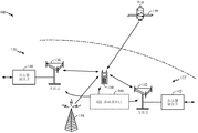
도 1은 상이한 무선 통신 시스템들(120, 122)과 통신하는 무선 디바이스(110)를 예시하는 도면(100)이다. 무선 통신 시스템들(120, 122)은 각각 CDMA(Code Division Multiple Access) 시스템, GSM(Global System for Mobile Communications) 시스템, LTE(Long Term Evolution) 시스템, WLAN(wireless local area network) 시스템, 또는 일부 다른 무선 시스템일 수 있다. CDMA 시스템은 WCDMA(Wideband CDMA), CDMA 1X 또는 cdma2000, TD-SCDMA(Time Division Synchronous Code Division Multiple Access), 또는 일부 다른 버전의 CDMA를 구현할 수 있다. TD-SCDMA는 또한 UTRA(Universal Terrestrial Radio Access) TDD(Time Division Duplex) 1.28 Mcps 옵션 또는 LCR(Low Chip Rate)로서 지칭된다. LTE는 FDD(Frequency Division Duplexing) 및 TDD(Time Division Duplexing) 둘 다를 지원한다. 예를 들어, 무선 통신 시스템(120)은 GSM 시스템일 수 있고, 무선 통신 시스템(122)은 WCDMA 시스템일 수 있다. 다른 예를 들면, 무선 통신 시스템(120)은 LTE 시스템일 수 있고, 무선 통신 시스템(122)는 CDMA 시스템일 수 있다. [0026]
FIG. 1 is a drawing 100 illustrating a
[0027]
단순함을 위해, 도면(100)은 하나의 기지국(130) 및 하나의 시스템 제어기(140)를 포함하는 무선 통신 시스템(120) 및 하나의 기지국(132) 및 하나의 시스템 제어기(142)를 포함하는 무선 통신 시스템(122)을 도시한다. 일반적으로, 각각의 무선 시스템은 임의의 수의 기지국들 및 임의의 세트의 네트워크 엔티티들을 포함할 수 있다. 각각의 기지국은 기지국의 커버리지 내의 무선 디바이스들을 위한 통신을 지원할 수 있다. 기지국들은 또한 노드 B, 이볼브드 노드 B(eNB), 액세스 포인트, 기지국 트랜시버, 무선 기지국, 무선 트랜시버 스테이션, 트랜시버 기능, 기본 서비스 세트(BSS: basic service set), 확장 서비스 세트(ESS: extended service set) 또는 다른 적합한 용어로 지칭될 수도 있다. 무선 디바이스(110)은 또한 UE(user equipment), 모바일 디바이스, 원격 디바이스, 무선 디바이스, 무선 통신 디바이스, 스테이션, 모바일 스테이션, 가입자 스테이션, 모바일 가입자 스테이션, 단말, 모바일 단말, 원격 단말, 무선 단말, 액세스 단말, 클라이언트, 모바일 클라이언트, 모바일 유닛, 가입자 유닛, 무선 유닛, 원격 유닛, 핸드셋, 사용자 에이전트 또는 일부 다른 적합한 용어로서 지칭될 수 있다. 무선 디바이스(110)는 셀룰러 전화, 스마트폰, 태블릿, 무선 모뎀, 개인용 디지털 보조기기(PDA), 핸드헬드 디바이스, 랩톱 컴퓨터, 스마트북, 넷북, 코드리스 전화, 무선 로컬 루프(WLL) 스테이션, 또는 일부 다른 유사한 기능 디바이스일 수 있다. [0027]
For simplicity, the drawing 100 includes a
[0028]
무선 디바이스(110)는 무선 통신 시스템(120 및/또는 122)과 통신 가능할 수 있다. 무선 디바이스(110)는 또한 브로드캐스트 스테이션(134)과 같은 브로드캐스트 스테이션으로부터 신호들을 수신 가능할 수 있다. 무선 디바이스(110)는 또한 하나 또는 그 초과의 글로벌 내비게이션 위성 시스템(GNSS)에서, 위성(150)과 같은 위성들로부터 신호들을 수신 가능할 수 있다. 무선 디바이스(110)는 GSM, WCDMA, cdma2000, LTE, 802.11 등과 같이 무선 통신 위한 하나 또는 그 초과의 라디오 기술들을 지원할 수 있다. "라디오 기술", "라디오 액세스 기술", "에어 인터페이스" 및 "표준"이란 용어들은 상호 교환 가능하게 이용될 수 있다. [0028]
The
[0029]
무선 디바이스(110)는 다운링크 및 업링크를 통해 무선 시스템의 기지국과 통신할 수 있다. 다운링크(또는 순방향 링크)는 기지국으로부터 무선 디바이스로의 통신 링크를 지칭하고, 업링크(또는 역방향 링크)는 무선 디바이스로부터 기지국으로의 통신 링크를 지칭한다. 무선 시스템은 TDD 및/또는 FDD를 활용할 수 있다. TDD의 경우, 다운링크 및 업링크는 동일한 주파수를 공유하고, 다운링크 전송들 및 업링크 전송들은 상이한 시간 기간들에서 동일한 주파수 상에서 전송될 수 있다. FDD의 경우, 다운링크 및 업링크에는 별개의 주파수들이 할당된다. 다운링크 전송들은 하나의 주파수 상에서 전송될 수 있고, 업링크 전송들은 다른 주파수 상에서 전송될 수 있다. TDD를 지원하는 일부 예시적인 라디오 기술은 GSM, LTE 및 TD-SCDMA를 포함한다. FDD를 지원하는 일부 예시적인 라디오 기술들은 WCDMA, cdma2000, 및 LTE를 포함한다. 무선 디바이스(110) 및/또는 기지국들(130, 132)은 예시적인 VCO 레귤레이터(160)를 포함할 수 있다. VCO 레귤레이터(160)는 이하에 제공된다. [0029]
The
[0030]
도 2는 무선 디바이스(110)와 같은 예시적인 무선 디바이스의 블록도(200)이다. 무선 디바이스는 데이터 프로세서/제어기(210), 트랜시버(218) 및 안테나(290)를 포함한다. 데이터 프로세서/제어기(210)는 프로세싱 시스템으로서 지칭될 수 있다. 프로세싱 시스템은 데이터 프로세서/제어기(210) 또는 데이터 프로세서/제어기(210) 및 메모리(216) 둘 다를 포함할 수 있다. 트랜시버(218)는 양-방향 통신을 지원하는 송신기(220) 및 수신기(250)를 포함한다. 송신기(220) 및/또는 수신기(250)는 수퍼-헤테로다인(super-heterodyne) 아키텍처 또는 직접-변환 아키텍처로 구현될 수 있다. 수퍼-헤테로다인 아키텍처에서, 신호는 다수의 스테이지들에서, 예를 들어, 일 스테이지에서 RF로부터 중간 주파수(IF)로 그리고 그 후, 수신기에 대한 다른 스테이지에서 IF로부터 기저대역으로 RF와 기저대역 간에 주파수-변환된다. 제로-IF 아키텍처로서 또한 지칭되는 직접-변환 아키텍처에서, 신호는 일 스테이지에서 RF와 기저대역 간에 주파수 변환된다. 수퍼-헤테로다인 및 직접-변환 아키텍처들은 상이한 회로 블록들을 이용하고 및/또는 상이한 요건들을 가질 수 있다. 도 2에 도시된 예시적인 설계에서, 송신기(220) 및 수신기(250)는 직접-변환 아키텍처로 구현된다. [0030]
FIG. 2 is a block diagram 200 of an exemplary wireless device, such as
[0031]
송신 경로에서, 데이터 프로세서/제어기(210)는 송신될 데이터를 프로세싱(예를 들어, 인코딩 및 변조)하고 데이터를 DAC(digital-to-analog converter)(230)에 제공할 수 있다. DAC(230)는 디지털 입력 신호를 아날로그 출력 신호로 변환한다. 아날로그 출력 신호는, DAC(230)에 의한 이전의 디지털-아날로그 변환에 의해 야기된 이미지를 제거하기 위해 아날로그 출력 신호를 필터링할 수 있는 송신(TX) 기저대역(저역통과) 필터(232)에 제공된다. 증폭기(amp)(234)는 TX 기저대역 필터(232)로부터의 신호를 증폭하고 증폭된 기저대역 신호를 제공할 수 있다. 상향변환기(믹서)(236)는 TX LO 신호 생성기(276)로부터의 TX LO 신호 및 증폭된 기저대역 신호를 수신할 수 있다. 상향 변환기(236)는 증폭된 기저대역 신호를 TX LO 신호로 상향 변환하고 상향변환된 신호를 제공할 수 있다. 필터(238)는 상향변환된 신호를 필터링하여 주파수 상향 변환에 의해 야기된 이미지들을 제거할 수 있다. 전력 증폭기(PA)(240)는, 원하는 출력 전력 레벨을 획득하고 출력 RF 신호를 제공하도록 필터(238)로부터의 필터링된 RF 신호를 증폭할 수 있다. 출력 RF 신호는 듀플렉서/스위치플렉서(264)를 통해 라우팅될 수 있다. [0031]
In the transmit path, the data processor /
[0032]
FDD의 경우, 송신기(220) 및 수신기(250)는 송신기(220)에 대한 TX 필터 및 수신기(250)에 대한 수신(RX) 필터를 포함할 수 있는 듀플렉서(264)에 커플링될 수 있다. TX 필터는 송신 대역의 신호 컴포넌트들을 통과시키고 수신 대역의 신호 컴포넌트들을 감쇠시키도록 출력 RF 신호를 필터링할 수 있다. TDD의 경우, 송신기(220) 및 수신기(250)는 스위치플렉서(264)에 커플링될 수 있다. 스위치플렉서(264)는 업링크 시간 인터벌들 동안 송신기(220)로부터의 출력 RF 신호를 안테나(290)로 전달할 수 있다. FDD 및 TDD 둘 다에 대해, 듀플렉서/스위치플렉서(264)는 무선 채널을 통한 송신을 위해 출력 RF 신호를 안테나(290)에 제공할 수 있다. [0032]
For FDD, the
[0033]
수신 경로에서, 안테나(290)는 기지국들 및/또는 다른 송신기 스테이션들에 의해 송신된 신호들을 수신할 수 있고 수신된 RF 신호를 제공할 수 있다. 수신된 RF 신호는 듀플렉서/스위치플렉서(264)를 통해 라우팅될 수 있다. FDD의 경우, 듀플렉서(264) 내의 RX 필터는 수신 대역의 신호 컴포넌트를 통과시키고 송신 대역의 신호 컴포넌트를 감쇠시키도록 수신된 RF 신호를 필터링할 수 있다. TDD의 경우, 스위치플렉서(264)는 다운링크 시간 인터벌들 동안 안테나(290)로부터의 수신된 RF 신호를 수신기(250)에 전달할 수 있다. FDD 및 TDD 둘 다에 대해, 듀플렉서/스위치플렉서(264)는 수신된 RF 신호를 수신기(250)에 제공할 수 있다. [0033]
In the receive path, the
[0034]
수신기(250) 내에서, 수신된 RF 신호는 LNA(low noise amplifier)(252)에 의해 증폭되고 필터(254)에 의해 필터링되어 입력 RF 신호를 획득할 수 있다. 하향변환기(믹서)(256)는 RX LO 신호 생성기(286)로부터 RX LO 신호 및 입력 RF 신호를 수신할 수 있다. 하향변환기(256)는 RX LO 신호로 입력 RF 신호를 하향변환하고 하향변환된 신호를 제공할 수 있다. 하향변환된 신호는 증폭기(258)에 의해 증폭되고, RX 기저대역(저역 통과) 필터(260)에 의해 추가로 필터링되어 아날로그 입력 신호를 획득할 수 있다. 아날로그 입력 신호는 ADC(analog-to-digital converter)(262)에 제공된다. ADC(262)는 아날로그 입력 신호를 디지털 출력 신호로 변환한다. 디지털 출력 신호는 데이터 프로세서/제어기(210)에 제공된다. [0034]
Within the
[0035]
TX 주파수 합성기(270)는 TX 위상 로킹 루프(PLL)(272) 및 VCO(274)를 포함할 수 있다. VCO(274)는 원하는 주파수의 TX VCO 신호를 생성할 수 있다. TX PLL(272)은 데이터 프로세서/제어기(210)로부터 타이밍 정보를 수신하고 VCO(274)에 대한 제어 신호를 생성할 수 있다. 제어 신호는 TX VCO 신호에 대한 원하는 주파수를 획득하기 위해 VCO(274)의 위상 및/또는 주파수를 조정할 수 있다. TX 주파수 합성기(270)는 TX VCO 신호를 TX LO 신호 생성기(276)에 제공한다. TX LO 신호 생성기는 TX 주파수 합성기(270)로부터 수신된 TX VCO 신호에 기초하여 TX LO 신호를 생성할 수 있다. [0035]
[0036]
RX 주파수 합성기(280)는 RX PLL(282) 및 VCO(284)를 포함할 수 있다. VCO(284)는 원하는 주파수의 RX VCO 신호를 생성할 수 있다. RX PLL(282)은 데이터 프로세서/제어기(210)로부터 타이밍 정보를 수신하고 VCO(284)에 대한 제어 신호를 생성할 수 있다. 제어 신호는 RX VCO 신호에 대한 원하는 주파수를 획득하기 위해 VCO(284)의 위상 및/또는 주파수를 조정할 수 있다. RX 주파수 합성기(280)는 RX LO 신호 생성기(286)에 RX VCO 신호를 제공한다. RX LO 신호 생성기는 RX 주파수 합성기(280)로부터 수신된 RX VCO 신호에 기초하여 RX LO 신호를 생성할 수 있다. [0036]
The
[0037]
LO 신호 생성기들(276, 286)은 각각 주파수 분할기, 버퍼 등을 포함할 수 있다. LO 신호 생성기들(276, 286)은 각각, 이들이 TX 주파수 합성기(270) 및 RX 주파수 합성기(280)에 의해 제공된 주파수를 분할하는 경우 주파수 분할기들로서 지칭될 수 있다. PLL들(272, 282)은 각각 위상/주파수 검출기, 루프 필터, 전하 펌프, 주파수 분할기 등을 포함할 수 있다. 각각의 VCO 신호 및 각각의 LO 신호는 특정 기본 주파수를 갖는 주기적 신호일 수 있다. LO 신호 생성기들(276, 286)로부터의 TX LO 신호 및 RX LO 신호는 TDD에 대해 동일한 주파수 또는 FDD에 대해 상이한 주파수를 가질 수 있다. VCO들(274, 284)로부터의 TX VCO 신호 및 RX VCO 신호는 동일한 주파수(예를 들어, TDD의 경우) 또는 상이한 주파수들(예를 들어, FDD 또는 TDD의 경우)을 가질 수 있다. [0037]
[0038]
송신기(220) 및 수신기(250)에서 신호들의 컨디셔닝은 증폭기, 필터, 상향변환기, 하향변환기 등의 하나 또는 그 초과의 스테이지들에 의해 수행될 수 있다. 이들 회로들은 도 2에서 도시된 구성과 상이하게 배열될 수 있다. 또한, 도 2에서 도시되지 않은 다른 회로들이 또한 송신기(220) 및 수신기(250)에서 신호들을 컨디셔닝하는데 이용될 수 있다. 예를 들어, 임피던스 매칭 회로는 PA(240)의 출력에, LNA(252)의 입력에, 안테나(290)와 듀플렉서/스위치플렉서(264) 사이 등에 로케이팅될 수 있다. 도 2의 일부 회로들은 또한 생략될 수 있다. 예를 들어, 필터(238) 및/또는 필터(254)는 생략될 수 있다. 트랜시버들(218) 중 일부 또는 모두 다는 하나 또는 그 초과의 아날로그 집적 회로들(IC들), RF IC들(RFIC들), 믹싱된-신호 IC들 등 상에서 구현될 수 있다. 예를 들어, 송신기(220)의 TX 기저대역 필터(232) 내지 PA(240), 수신기(250)의 LNA(252) 내지 RX 기저대역 필터(260), PLL들(272, 282), VCO들(274, 284) 및 LO 신호 생성기들(276, 286)은 RFIC 상에 구현될 수 있다. PA(240) 및 가능하게는 다른 회로들이 또한 별개의 IC 또는 회로 모듈 상에서 구현될 수 있다. [0038]
Conditioning of signals at
[0039]
데이터 프로세서/제어기(210)는 무선 디바이스에 대한 다양한 기능들을 수행할 수 있다. 예를 들어, 데이터 프로세서/제어기(210)는 송신기(220)를 통해 송신되고 수신기(250)를 통해 수신되는 데이터에 대한 프로세싱을 수행할 수 있다. 데이터 프로세서/제어기(210)는 송신기(220) 및 수신기(250) 내의 다양한 회로들의 동작을 제어할 수 있다. 메모리(212) 및/또는 메모리(216)는 데이터 프로세서/제어기(210)에 대한 프로그램 코드들 및 데이터를 저장할 수 있다. 메모리는 데이터 프로세서/제어기(210) 내부 (예를 들어, 메모리(212)) 또는 데이터 프로세서/제어기(210) 외부 (예를 들어, 메모리(216))에 있을 수 있다. 메모리는 컴퓨터-판독 가능 매체로서 지칭될 수 있다. 오실레이터(214)는 특정 주파수의 VCO 신호를 생성할 수 있다. 클록 생성기(215)는 오실레이터(214)로부터 VCO 신호를 수신할 수 있고 데이터 프로세서/제어기(210) 내의 다양한 모듈들에 대한 클럭 신호들을 생성할 수 있다. 데이터 프로세서/제어기(210)는 하나 또는 그 초과의 주문형 집적 회로들(ASIC들) 및/또는 다른 IC들 상에 구현될 수 있다. [0039]
The data processor /
[0040]
LO 신호 발생기들(276, 286)의 주파수 분할기들과 같은 주파수 분할기들은 LO 신호들을 생성하기 위해 광범위하게 사용된다. 작은 칩 면적, 양호한 위상 노이즈 요건 및 직교 출력(quadrature output)과 같은 엄격한 LO 요건들을 충족하는 다중-대역 셀룰러 트랜시버들에서 LO 신호들을 생성하기 위한 프로그래밍 가능 주파수 분할기에 대한 필요성이 존재한다. [0040]
Frequency dividers, such as frequency dividers of
[0041]
VCO(예를 들어, 도 2의 VCO(274) 또는 VCO(284))는 노이즈 스파이크들 및 스퍼들(spurs)에 민감하다. 따라서, PMIC(power management integrated circuit)는 일반적으로 이러한 문제를 해결하기 위해 VCO에 대해 사용된다. PMIC 노이즈/스퍼 프로파일에 기초하여, 1MHz에서 적어도 40dB의 PSRR(Power Supply Rejection Ratio)이 일반적으로 바람직하다. 예를 들어, 노이즈의 스퍼(예를 들어, 스파이크)는 PMIC 노이즈/스퍼 프로파일에서 100kHz 내지 1MHz에서 관찰된다. 따라서, 양호한 대역폭(예를 들어, 넓은 대역폭)을 제공하고 VCO에 대한 스퍼(예를 들어, 큰 스파이크)를 감쇠시킬 수 있는 효과적인 VCO 레귤레이터에 대한 요구가 존재한다. 보다 넓은 PSRR 대역폭이 VCO 레귤레이터의 개선된 성능을 제공할 수는 있지만, PSRR 대역폭을 증가시키는 것은 또한 노이즈 대역폭을 증가시킬 수 있다는 점에 유의해야 한다. 따라서, PSRR 대역폭을 증가시키는 것과 바람직하지 않은 노이즈 대역폭을 증가시키는 것 간의 트레이드-오프가 있다. [0041]
The VCO (e.g.,
[0042] VCO가 원하는 전력/위상 노이즈 조건들을 획득하기 위해, VCO는 전압을 공급하는 이중 공급 구성을 갖는 VCO 레귤레이터를 구현할 수 있다. 이중 공급 구성은 VCO의 공급/전자기 풀링(pulling)을 완화할 수 있다. 예를 들어, 이중 전압 공급 구성은 GSM 모드에 대해 고전압(HV)을 공급할 수 있고, 비-GSM 모드(예를 들어, CDMA, LTE 등)에 대해 저전압(LV)을 공급할 수 있다. LV 비-GNS 모드의 경우, LV 비-GSM 모드에서 VCO 레귤레이터에 공급된 전압이 낮기 때문에, 저전압에 대한 특정 LV PSRR은 VCO 레귤레이터의 만족스러운 성능에 대한 관심사이다. 예를 들어, 저전압을 공급하는 LV 비-GSM 모드에서, PMIC 펄스-주파수 변조(PFM) 스퍼들을 완화하기 위해, VCO 레귤레이터는 100mV 미만의 드롭아웃 전압으로 수백 KHz 내지 MHz 범위에서 약 100dB의 LV PSRR을 제공해야 한다. 예시적인 시뮬레이션 결과들은, LV 비-GSM 모드에 대해, PMIC PFM 스퍼들을 완화하기 위해 100KHz에서 약 100dB의 PSRR이 요구된다는 것을 예시한다. HV GSM 모드에 대해, VCO 레귤레이터에 공급되는 고전압이 노이즈 대역폭을 증가시킬 수 있기 때문에, 양호한 노이즈 성능은 VCO 레귤레이터의 만족스러운 성능에 대한 관심사이다. 예를 들어, 고전압을 공급하는 HV GSM 모드에서, VCO 레귤레이터는 고전압에 대해 낮은 노이즈를 유지하면서, 수십 MHz 범위의 주파수에서 특정 PSRR을 제공한다. [0042] To obtain the desired power / phase noise conditions of the VCO, the VCO may implement a VCO regulator having a dual supply configuration that supplies a voltage. The dual supply configuration can mitigate the supply / electromagnetic pulling of the VCO. For example, a dual voltage supply configuration can supply a high voltage (HV) for the GSM mode and a low voltage (LV) for a non-GSM mode (e.g., CDMA, LTE, etc.). In the LV non-GNS mode, the specific LV PSRR for the low voltage is a concern for the satisfactory performance of the VCO regulator, since the voltage supplied to the VCO regulator in the LV non-GSM mode is low. For example, to mitigate PMIC pulse-frequency modulation (PFM) spurs in an LV non-GSM mode that provides a low voltage, the VCO regulator has an LV PSRR of about 100 dB at a dropout voltage of less than 100 mV and in the range of hundreds of KHz to MHz . Exemplary simulation results illustrate that for the LV non-GSM mode, a PSRR of about 100 dB at 100 KHz is required to mitigate PMIC PFM spurs. For the HV GSM mode, good noise performance is a concern for the satisfactory performance of the VCO regulator because the high voltage supplied to the VCO regulator can increase the noise bandwidth. For example, in the HV GSM mode, which supplies a high voltage, the VCO regulator provides a specific PSRR at frequencies in the range of tens of MHz, while maintaining low noise for high voltages.
[0043] VCO 레귤레이터는 다양한 PSRR/노이즈 규격을 만족시키고 PSRR과 노이즈 간의 트레이드 오프에 대해 적응하도록 프로그래밍 가능(예를 들어, 튜닝 가능)한 것이 바람직하다. 예를 들어, VCO 레귤레이터는 다른 용도들을 위해 상이한 PSRR 및 노이즈 특성들을 제공하도록 프로그래밍 가능해야 한다. 따라서, 예를 들어, VCO 레귤레이터는 모드가 LV 모드인지 또는 HV 모드 여부에 의존하여 상이한 PSRR 및 노이즈 특성들을 제공하도록 프로그래밍 가능해야 한다. [0043] The VCO regulator is preferably programmable (e.g., tunable) to meet various PSRR / noise specifications and to adapt for trade-off between PSRR and noise. For example, a VCO regulator should be programmable to provide different PSRR and noise characteristics for different uses. Thus, for example, the VCO regulator must be programmable to provide different PSRR and noise characteristics depending on whether the mode is the LV mode or the HV mode.
[0044] VCO 레귤레이터의 성능은 패스(pass) 엘리먼트의 타입(예를 들어, DC 바이어스, 입력/출력 임피던스)과 관련된다는 것에 유념한다. 일반적으로, N-타입 금속-산화물-반도체(NMOS) 레귤레이터는 DC 바이어스 조건에 의해 제한되며, P-형 금속-산화물-반도체(PMOS) 레귤레이터는 NMOS 레귤레이터보다 더 안 좋은 PSRR을 갖는다. 표 1은 NMOS 레귤레이터와 PMOS 레귤레이터 간의 비교를 예시한다. 표 1에서, 플러스 부호들(+)의 수는 바람직한 성능의 정도를 나타내고, 마이너스 부호들(-)의 수는 바람직하지 않은 성능의 정도를 나타낸다. [0044] Note that the performance of the VCO regulator is related to the type of pass element (e.g., DC bias, input / output impedance). In general, an N-type metal-oxide-semiconductor (NMOS) regulator is limited by DC bias conditions and a P-type metal-oxide-semiconductor (PMOS) regulator has a worse PSRR than an NMOS regulator. Table 1 illustrates a comparison between an NMOS regulator and a PMOS regulator. In Table 1, the number of plus signs (+) represents the degree of desired performance and the number of minus signs (-) represents the degree of undesirable performance.

표 1 : NMOS 레귤레이터와 PMOS 레귤레이터 간의 비교Table 1: Comparison between NMOS regulators and PMOS regulators
[0045]
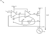
본 개시에 따른 NMOS 레귤레이터는 바람직한 PSRR(예를 들어, 100dB)을 획득하기 위해 2-스테이지 동작 트랜스컨덕턴스 증폭기(OTA) 회로를 구현한다. 2-스테이지 OTA 회로는 보상 네트워크를 통해 100kHz에서 100dB를 획득하도록 대역폭을 제한할 수 있다. 2-스테이지 OTA 회로의 보상 네트워크는 또한 극 소거(pole cancellation)를 제공한다. 도 3은 본 개시에 따른 NMOS 레귤레이터의 예시적인 회로도(300)이다. NMOS 레귤레이터(300)는 NMOS(302)를 포함한다. NMOS(302)는 소스(S), 드레인(D) 및 게이트(G)를 갖는다. NMOS 레귤레이터(300)는 2-스테이지 OTA 회로를 제공하기 위해 제 1 증폭기(304) 및 제 2 증폭기(306)를 포함한다. 제 2 증폭기(306)는 공통 소스 증폭기일 수 있다. 예를 들어, 60-70dB의 PSSR은 제 1 증폭기(304)를 통해 제 1 스테이지에서 달성될 수 있고, 30-40dB의 PSSR은 제 2 증폭기(306)를 통해 제 2 스테이지에서 달성될 수 있으며, 그에 의해 2-스테이지 OTA 회로에 대해 대략 100dB의 총 PSSR이 달성된다. 제 1 증폭기(304)의 출력은 제 2 증폭기(306)의 입력에 연결되고, 제 2 증폭기(306)의 출력은 NMOS(302)의 게이트(G)에 연결된다. 제 1 증폭기(304)의 출력은 또한 커패시터(308)의 제 1 단부에서 커패시턴스(CM)를 갖는 커패시터(308)에 연결된다. 커패시터(308)의 제 2 단부는 저항(RM)을 갖는 레지스터(310)의 제 1 단부에 연결된다. 레지스터(310)의 제 2 단부는 NMOS(302)의 소스(S) 및 VCO(350)에 연결된다. VCO(350)는 도 2의 VCO(274) 또는 VCO(284)와 등가일 수 있다. [0045]
An NMOS regulator in accordance with the present disclosure implements a two-stage operational transconductance amplifier (OTA) circuit to obtain a desired PSRR (e.g., 100 dB). The 2-stage OTA circuit can limit the bandwidth to achieve 100dB at 100kHz through the compensation network. The compensation network of the two-stage OTA circuit also provides pole cancellation. 3 is an exemplary circuit diagram 300 of an NMOS regulator in accordance with the present disclosure. The
[0046]
커패시터(308) 및 레지스터(310)는 제 1 증폭기(304)를 포함하는 제 1 스테이지 OTA 회로의 출력으로 레귤레이터 출력(312)을 보상하기 위한 보상 네트워크를 형성한다. 커패시터(308) 및 레지스터(310)는 제 1 스테이지 OTA 회로의 트랜스컨덕턴스(Gm)와 매칭될 수 있다. 예를 들어, 커패시터(308) 및 레지스터(310)를 포함하는 보상 네트워크는 노이즈를 최소화하고 안정성을 위해 제 1 스테이지 OTA 회로의 Gm과 매칭하도록 튜닝 가능할 수 있다. 보상 네트워크 및 제 1 스테이지 OTA 회로 둘 다는 서로 매칭하도록 튜닝 가능하다는 것에 유념한다. 보상 네트워크 또는 제 1 스테이지 OTA 회로 중 적어도 하나가 튜닝 가능하기 때문에, 레귤레이터는 양호한 안정성, 양호한 레귤레이터 대역폭 및 낮은 노이즈를 유지할 수 있다. 제 1 스테이지 OTA Gm이 더 큰 경우, 보상 네트워크가 더 강한 보정을 제공하고, 이에 따라 더 양호한 안정성을 제공한다는 것에 유념한다. [0046]
The
[0047]
다음의 수식들은 도 3에 예시된 예에 따른 PSRR의 계산을 제공한다. Apath는 도 3에서 도시된 Apath를 통한 이득이다. s는 jω이다. A는 레귤레이터 출력(312)에 대한 공급부(supply)로부터의 DC 이득이다. A2는 제 2 증폭기(306)에서의 DC 이득이다. ro1은 제 1 증폭기(304)의 출력 저항이다. ωp1은 제 1 증폭기(304)의 출력에서의 극(pole)이고, ωp2는 제 2 증폭기(306)의 출력에서의 극이고, ωp3은 NMOS 레귤레이터의 출력(312)에서의 극이다. ωz는 레지스터(310) 및 커패시터(308)를 갖는 보상 네트워크에 의해 생성된 0이다. ALP는 제 1 증폭기(304)의 입력으로부터 레귤레이터 출력(312)까지의 개방 루프 DC 이득이다. [0047] The following equations provide a calculation of the PSRR according to the example illustrated in FIG. A path is a gain through A path shown in FIG. s is jω. A is the DC gain from the supply to the


[0048]
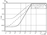
도 4a는 레귤레이터의 다양한 경우에서의 PSSR 값들의 예시적인 PSSR 플롯(400)이다. PSSR 플롯(400)은, 극 소거(PC) 2-스테이지 OTA 레귤레이터 회로가 1-스테이지 OTA 레귤레이터 및 종래의 2-스테이지 OTA 레귤레이터의 PSSR 플롯보다 -100dB의 바람직한 PSSR에 더 가까운 PSSR 플롯을 제공한다는 것을 예시한다. 따라서, (예를 들어, 도 3의 NMOS 레귤레이터를 통해) 본 개시의 2-스테이지 OTA 레귤레이터 회로에 의해 제공되는 극 소거는 PSSR의 대역폭을 확장하는 것을 돕는다. 2-스테이지 OTA 정규 회로가 제공하는 전력이 많을수록, PSSR 대역폭은 더 넓다. 도 4b는 다양한 경우에서의 노이즈 값들의 예시적인 노이즈 플롯(450)이다. 예시적인 노이즈 플롯(450)에 따라, PC 2-스테이지 OTA 레귤레이터 회로의 노이즈 플롯은, 부분(452)을 제외하면, 1-스테이지 OTA 레귤레이터 및 종래의 2-스테이지 OTA 레귤레이터의 노이즈 플롯들과 유사하다. 예시적인 노이즈 플롯(450)의 부분(452)은 획대된 부분(454)에서 확대된다. 확대된 부분(454)은 PC 2-스테이지 OTA 레귤레이터 회로 및 종래의 2-스테이지 OTA 정규 회로 둘 다가 1-스테이지 OTA 정규 회로보다 약간 더 높은 노이즈를 경험한다는 것을 나타낸다. [0048]
4A is an
[0049]
도 5는 본 개시에 따른 NMOS 레귤레이터의 예시적인 구현 회로(500)이다. NMOS 레귤레이터(500)는 레지스터 및 커패시터를 포함하는 보상 네트워크 및 2개의 OTA들을 포함하는 2-스테이지 OTA 회로(502)를 포함한다. 일 양상에서, 2-스테이지 OTA 회로(502)는 도 3의 제 1 증폭기(304) 및 제 2 증폭기(306)를 포함하는 2-스테이지 OTA 회로와 등가일 수 있다. 일 양상에서, 보상 네트워크(504)는 도 3의 커패시터(308) 및 레지스터(310)를 포함하는 보상 네트워크와 등가일 수 있다. 보상 네트워크(504)는 2-스테이지 OTA 회로(502)의 제 1 스테이지 OTA 회로와 매칭하도록 튜닝 가능할 수 있다. [0049]
5 is an
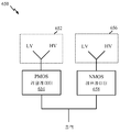
[0050] 본 개시에 따라, 레귤레이터 회로는 PMOS 레귤레이터 및 NMOS 레귤레이터를 포함하는 상보적 금속-산화물-반도체(CMOS) 레귤레이터 회로일 수 있으며, 여기서 NMOS 레귤레이터는 PMOS 레귤레이터에 커플링된다. 일 양상에서, PMOS 레귤레이터는 NMOS 레귤레이터에 직렬로(캐스코드로) 연결될 수 있다. 다른 양상에서, PMOS 레귤레이터는 NMOS 레귤레이터에 병렬로 연결될 수 있다. 레귤레이터 회로는 스위치 회로에 연결되어 CMOS 레귤레이터 회로에 대해 HV 모드 또는 LV 모드를 선택적으로 선택할 수 있다. 일반적으로, VCO에 대해, HV 모드는 보다 적은 풀링 효과 및 보다 양호한 위상 노이즈 성능의 관점에서 보다 양호한 성능을 위해 사용될 수 있다. 그러나 HV 모드는 더 높은 전력 소모를 유발할 수 있다. LV 모드는 일반적으로 HV 모드보다 더 낮은 전력 소비를 유발한다. VCO는 HV 모드에서 전자기(EM) 커플링에 덜 민감하다는 점에 또한 유념한다. 일 양상에서, 스위치 회로는 PMOS 레귤레이터에 대해 HV 모드를 선택하고 NMOS 레귤레이터를 우회할 수 있다. 다른 양상에서, LV 모드에 대해, 스위치 회로는 NMOS 레귤레이터를 선택하고 PMOS 레귤레이터를 우회할 수 있거나, PMOS 레귤레이터 및 NMOS 레귤레이터를 둘 다를 선택할 수 있다. 또한, PMOS 레귤레이터 및 NMOS 레귤레이터는 상이한 입력 임피던스 및 출력 임피던스를 갖는다는 것에 유념한다. PMOS 레귤레이터는 일반적으로 NMOS 레귤레이터보다 더 낮은 입력 임피던스 및 더 높은 출력 임피던스를 갖는다. 따라서, 일 양상에서, 스위치 회로는 VCO가 주변 빌딩 블록들에 대한 침입자(aggressor)인지 희생자(victim)인지에 의존하여 PMOS 레귤레이터 또는 NMOS 레귤레이터 중 어느 하나를 선택하는데 사용될 수 있다. 예를 들어, 스위치 회로는, (예를 들어, 주변 빌딩 블록들을 풀링함으로써) VCO가 주변 빌딩 블록에 영향을 줄 수 있는 침입자인 경우, PMOS 레귤레이터를 선택할 수 있다. 예를 들어, 스위치 회로는, (예를 들어, 주변 빌딩 블록들에 의해 풀링됨으로써) VCO가 주변 빌딩 블록들에 의해 영향을 받을 수 있는 희생자인 경우, NMOS 레귤레이터를 선택할 수 있다. 직렬로 연결된 PMOS 레귤레이터 및 NMOS 레귤레이터 둘 다를 선택하는 것은 또한 주변 빌딩 블록들로부터 영향을 받는 것 및/또는 주변 빌딩 블록들에 영향을 미치는 것으로부터 격리를 제공할 것이란 점에 추가로 유념한다. [0050] According to the present disclosure, the regulator circuit may be a complementary metal-oxide-semiconductor (CMOS) regulator circuit including a PMOS regulator and an NMOS regulator, wherein the NMOS regulator is coupled to the PMOS regulator. In an aspect, a PMOS regulator may be coupled (in cascade) in series with the NMOS regulator. In another aspect, the PMOS regulator may be connected in parallel to the NMOS regulator. The regulator circuit is connected to the switch circuit so that the HV mode or the LV mode can be selectively selected for the CMOS regulator circuit. In general, for a VCO, the HV mode can be used for better performance in terms of less pulling effect and better phase noise performance. However, HV mode can lead to higher power consumption. LV mode generally causes lower power consumption than HV mode. It is also noted that the VCO is less sensitive to electromagnetic (EM) coupling in HV mode. In an aspect, the switch circuit may select the HV mode for the PMOS regulator and bypass the NMOS regulator. In another aspect, for LV mode, the switch circuit may select an NMOS regulator and bypass the PMOS regulator, or both a PMOS regulator and an NMOS regulator. It should also be noted that the PMOS regulator and the NMOS regulator have different input and output impedances. PMOS regulators generally have lower input impedance and higher output impedance than NMOS regulators. Thus, in an aspect, a switch circuit may be used to select either a PMOS regulator or an NMOS regulator depending on whether the VCO is an aggressor or a victim to neighboring building blocks. For example, a switch circuit may select a PMOS regulator if the VCO is an intruder that may affect surrounding building blocks (e.g., by pooling surrounding building blocks). For example, the switch circuit may select an NMOS regulator if the VCO is a victim to be affected by neighboring building blocks (e.g., by being pulled by neighboring building blocks). It is further noted that the selection of both a series connected PMOS regulator and an NMOS regulator will also provide isolation from being affected by surrounding building blocks and / or affecting neighboring building blocks.
[0051]
도 6a 및 도 6b는 CMOS 레귤레이터의 예시적인 구조들이다. 도 6a는 PMOS 레귤레이터(604) 및 NMOS 레귤레이터(606)가 직렬로 연결된 CMOS 레귤레이터의 예시적인 구조(600)이다. 특히, 스위치 회로(602)는 NMOS 레귤레이터(606)에 직렬로 연결되는 PMOS 레귤레이터(604)에 연결된다. 스위치 회로(602)는 LV 모드 및 HV 모드 중 하나를 선택하도록 구성된다. 위에서 논의된 바와 같이, 예를 들어, LV 모드는 비-GSM 모드에 대해 저전압을 공급하는데 사용되고, HV 모드는 GSM 모드에 대해 고전압을 공급하는데 사용된다. 도시되지는 않았지만, 다른 예에서, PMOS 레귤레이터(604) 및 NMOS 레귤레이터(606)의 순서는 도 6a의 예시적인 구조(600)와 다를 수 있다. CMOS 레귤레이터는 PMOS 레귤레이터 및 NMOS 레귤레이터를 포함한다. 도 6b는 PMOS 레귤레이터(654) 및 NMOS 레귤레이터(658)가 병렬로 연결된 CMOS 레귤레이터의 예시적인 구조(650)이다. 특히, 제 1 스위치 회로(652)는 PMOS 레귤레이터(654)에 연결되고, 제 2 스위치 회로(656)는 NMOS 레귤레이터(658)에 연결되며, 여기서 PMOS 레귤레이터(654)와 NMOS 레귤레이터(658)는 병렬로 연결된다. 위에서 논의된 바와 같이, 예를 들어, LV 모드는 비-GSM 모드에 대해 저전압을 공급하는데 사용되고, HV 모드는 GSM 모드에 대해 고전압을 공급하는데 사용된다. 따라서, LV 모드가 사용되면, 제 1 스위치 회로(652) 및 제 2 스위치 회로(656) 둘 다는 저전압을 제공하도록 구성된다. HV 모드가 사용되면, 제 1 스위치 회로(652) 및 제 2 스위치 회로(656) 둘 다는 고전압을 제공하도록 구성된다. [0051]
6A and 6B are exemplary structures of a CMOS regulator. 6A is an
[0052]
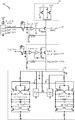
도 7은 캐스코드 CMOS 레귤레이터를 포함하는 예시적인 회로도(700)이다. 특히, 스위치 회로(710)는 PMOS 레귤레이터(730) 및 NMOS 레귤레이터(750)를 포함하는 CMOS 레귤레이터에 연결되며, 여기서 PMOS 레귤레이터(730) 및 NMOS 레귤레이터(750)는 직렬로(캐스코드) 연결된다. CMOS 레귤레이터는 NMOS 레귤레이터(750)를 통해 VCO 회로(770)에 연결된다. VCO 회로(770)는 도 2의 VCO(274) 또는 VCO(284)와 등가일 수 있다. VCO 회로(770)는 772에서의 저주파수(LF) VCO 출력을 그리고 774에서의 고주파수(HF) VCO 출력을 가질 수 있다. 일 양상에서, 스위치 회로(710)는 CMOS 레귤레이터에 대해 HV 모드의 전압 또는 LV 모드의 전압 중 어느 하나를 선택적으로 공급할 수 있다. 도 7의 예에서, 스위치 회로(710)는 1.6V의 HV 모드 전압 또는 0.95V의 LV 모드 전압을 CMOS 레귤레이터에 공급할 수 있다. 스위치 회로(710)는 다음과 같이 다양한 팩터들에 의존하여 HV 모드의 전압 또는 LV 모드의 전압 중 어느 하나를 선택적으로 공급할 수 있다. HV 모드는 LV 모드보다 더 양호한 VCO 위상 노이즈 및 스윙뿐만 아니라 더 양호한 VCO 버퍼 위상 노이즈 및 스윙을 제공할 수 있다. LV 모드는 HV 모드보다 더 낮은 전력 소비를 유발한다. CMOS 레귤레이터에 공급되는 전압의 공급 전압 도메인은 더 적은 공급 커플링을 경험하도록 구성될 수 있다. VCO는 LV 모드에서 보다 HV 모드에서 EM 커플링에 덜 민감하다는 점에 또한 유념한다. [0052]
7 is an exemplary circuit diagram 700 that includes a cascode CMOS regulator. In particular, the
[0053]
일 양상에서, NMOS 레귤레이터(750)는 PMOS 레귤레이터(730)보다 100MHz에서 더 양호한 PSRR을 갖는다. 일 양상에서, PMOS 레귤레이터(730)는 NMOS 레귤레이터(750)보다 100MHz에서(예를 들어, GSM에서, HV 및 낮은 PMOS 레귤레이터 BW) 더 양호한 노이즈 성능(예를 들어, 낮은 노이즈)을 가질 수 있다. 도 7의 예에서, PMOS 레귤레이터(730)는 Vdd = -50mV를 출력할 수 있다. 도 7의 예에서, NMOS 레귤레이터(750)는 100mV 드롭-아웃으로 1MHz에서 100dB의 PSRR을 달성할 수 있다. 예를 들어, NMOS 레귤레이터(750)는 PFM 스퍼들에 대해 1MHz에서 100dB의 PSRR을 달성하기 위해 2-스테이지 OTA 및 극 소거 특징들을 갖는다. [0053]
In an aspect,
[0054]
도 8은 버퍼 회로를 포함하는 예시적인 회로도(800)이다. 예시적인 회로도(800)에서, 스위치 회로(810)는 버퍼 회로(830)에 접속된다. 일 양상에서, 스위치 회로(810)는 HV 모드 또는 LV 모드 중 어느 하나를 선택적으로 제공할 수 있다. 버퍼 회로(830)는 도 7의 VCO 회로(770)와 같은 VCO로부터의 출력들을 수신하고 출력들을 버퍼링한다. 따라서, 버퍼 회로(830)는 도 7의 VCO 회로(770)에 연결될 수 있다. 예를 들어, 버퍼 회로(830)로의 LF VCO 입력(832)은 도 7의 LF VCO 출력(772)으로부터 올 수 있고 버퍼 회로(830)로의 HF VCO 입력(834)은 도 7의 HF VCO 출력(774)으로부터 올 수 있다. [0054]
8 is an exemplary circuit diagram 800 that includes a buffer circuit. In the exemplary circuit diagram 800, the
[0055]
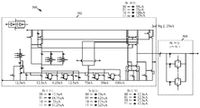
도 9는 본 개시에 따른 시스템 레벨에서의 예시적인 회로 구조(900)이다. 예시적인 회로 구조(900)는 송신(TX) VCO 레귤레이터(902), 제 1 수신(RX) 캐리어 어그리게이션(CA) 레귤레이터(904) 및 제 2 RX CA 레귤레이터(906)를 포함한다. 제 1 RX CA 레귤레이터(904)는 제 1 주파수에서 캐리어 어그리게이션을 수신하기 위한 것이고, 제 2 RX CA 레귤레이터(906)는 제 2 주파수에서 캐리어 어그리게이션을 수신하기 위한 것이다. TX VCO 레귤레이터(902), 제 1 RX CA 레귤레이터(904) 및 제 2 RX CA 레귤레이터(906) 각각의 것은 NMOS 레귤레이터에 커플링된 PMOS 레귤레이터를 갖는 CMOS 레귤레이터 구조를 포함한다. [0055]
9 is an
[0056]
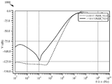
도 10a는 VCO의 다양한 경우에서의 PSSR 값들의 예시적인 PSSR 플롯(1000)이다. PSSR 플롯(1000)은, 2-스테이지 OTA 레귤레이터 회로가 1-스테이지 OTA 레귤레이터의 PSSR 플롯보다 -100dB의 바람직한 PSSR에 더 가까운 VCO에 대한 PSSR 플롯을 제공한다는 것을 예시한다. 따라서, 100kHz에서 100dB의 PSRR은 2-스테이지 OTA 레귤레이터에 의해 달성된다. 또한, 도 10a에 따라, 2-스테이지 OTA 레귤레이터가 사용될 때, VCO는 또한 50dB 개선을 경험할 수 있다. 도 10b는 VCO의 다양한 경우에서의 노이즈 값들의 예시적인 노이즈 플롯(1050)이다. 예시적인 노이즈 플롯(1050)에 따라, 1-스테이지 OTA 레귤레이터의 노이즈 플롯은 스퍼들(1052 및 1054)을 갖는 반면, 2-스테이지 OTA 레귤레이터의 노이즈 플롯은 스퍼들을 갖지 않는다. 따라서, 2-스테이지 OTA 레귤레이터가 사용될 때, VCO는 스퍼 감소를 경험한다. 또한, VCO VDD가 높은-공급 도메인(high-supply domain)으로 스위칭하는 경우, 4-5dB RSB(reference side band) 개선이 제공될 수 있다. [0056]
10A is an
[0057]
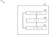
도 11은 레귤레이터 회로에 의한 방법의 흐름도(1100)이다. 이 방법은 레귤레이터 회로(예를 들어, 레귤레이터 회로(600, 650), 장치(1202/1202'))에 의해 수행될 수 있다. 1102에서, 레귤레이터 회로는 제 1 전압 레귤레이터를 통해, 제 1 전압 레귤레이터에 대한 제 1 입력 전압을 레귤레이팅하며, 제 1 전압 레귤레이터는 PMOS를 포함한다. 1104에서, 레귤레이터 회로는 제 2 전압 레귤레이터를 통해, 제 2 전압 레귤레이터에 대한 제 2 입력 전압을 레귤레이팅하며, 제 2 전압 레귤레이터는 NMOS를 포함하고, 여기서 제 1 전압 레귤레이터는 제 2 전압 레귤레이터에 연결된다. 1106에서, 레귤레이터 회로는 스위치 회로를 통해, 제 1 전압 레귤레이터 또는 제 2 전압 레귤레이터 중 적어도 하나를 선택적으로 활성화한다. 일 양상에서, 제 1 전압 레귤레이터 또는 제 2 전압 레귤레이터 중 적어도 하나는 노이즈에 기초하여 선택적으로 활성화된다. [0057]
11 is a
[0058]
도 12는 예시적인 장치(1202) 내의 상이한 모듈들/수단/컴포넌트들 사이의 데이터 흐름을 예시하는 개념적 데이터 흐름도(1200)이다. 장치는 레귤레이터 회로일 수 있다. 장치는 제 1 전압 레귤레이터 모듈(1204), 제 2 전압 레귤레이터 모듈(1206) 및 스위칭 모듈(1208)을 포함한다. [0058]
12 is a conceptual data flow diagram 1200 illustrating the flow of data between different modules / means / components in the
[0059]
제 1 전압 레귤레이터 모듈(1204)은 제 1 전압 레귤레이터 모듈(1204)에 대한 제 1 입력 전압을 레귤레이팅한다. 일 양상에서, 제 1 전압 레귤레이터 모듈(1204)은 PMOS를 포함한다. 제 2 전압 레귤레이터 모듈(1206)은 제 2 전압 레귤레이터 모듈(1206)에 대한 제 2 입력 전압을 레귤레이팅한다. 일 양상에서, 제 2 전압 레귤레이터 모듈(1206)은 NMOS를 포함한다. 일 양상에서, 제 1 전압 레귤레이터는 제 2 전압 레귤레이터에 연결된다. 스위칭 모듈(1208)은 제 1 전압 레귤레이터 모듈(1204) 또는 제 2 전압 레귤레이터 모듈(1206) 중 적어도 하나를 선택적으로 활성화시킨다. 일 양상에서, 제 1 전압 레귤레이터 모듈(1204) 또는 제 2 전압 레귤레이터(1206) 중 적어도 하나는 노이즈에 기초하여 선택적으로 활성화된다. [0059]
The first
[0060] 장치는 도 11의 상술된 흐름도들에서의 알고리즘의 블록들 각각을 수행하는 부가적인 모듈들을 포함할 수 있다. 이와 같이, 도 11의 상술된 흐름도들의 각각의 블록은 모듈에 의해 수행될 수 있고, 장치는 이들 모듈들 중 하나 또는 그 초과를 포함할 수 있다. 모듈들은 언급된 프로세스/알고리즘을 수행하도록 특별히 구성되고, 언급된 프로세스/알고리즘을 수행하도록 구성된 프로세서에 의해 구현되고, 프로세서에 의한 구현을 위해 컴퓨터-판독 가능 매체 내에 저장되거나, 또는 이들의 조합에 의해 이루어지는 하나 또는 그 초과의 하드웨어 컴포넌트들일 수 있다. [0060] The apparatus may comprise additional modules for performing each of the blocks of the algorithm in the flowcharts described above in Fig. As such, each block of the above-described flowcharts of FIG. 11 may be performed by a module, and the device may include one or more of these modules. The modules may be implemented by a processor configured to perform the described process / algorithm and configured to perform the mentioned process / algorithm, stored in a computer-readable medium for implementation by a processor, or a combination thereof Lt; / RTI > may be one or more hardware components.
[0061]
도 13은 프로세싱 시스템(1314)을 이용하는 장치(1202')에 대한 하드웨어 구현의 예를 예시하는 도면(1300)이다. 프로세싱 시스템(1314)은, 개괄적으로 버스(1324)로 표현되는 버스 아키텍쳐로 구현될 수 있다. 버스(1324)는 프로세싱 시스템(1314)의 특정 애플리케이션 및 전체적인 설계 제약들에 의존하여, 임의의 개수의 상호연결 버스들 및 브리지들을 포함할 수 있다. 버스(1324)는 프로세서(1304), 모듈들(1204, 1206, 1208), 및 컴퓨터-판독 가능 매체/메모리(1306)로 표현되는 하나 또는 그 초과의 프로세서들 및/또는 하드웨어 모듈들을 포함하는 다양한 회로들을 함께 링크한다. 버스(1324)는 또한 해당 기술분야에 잘 알려진, 그리고 이에 따라 더는 설명되지 않을, 타이밍 소스들, 주변 장치들, 전압 조정기들 및 전력 관리 회로들과 같은 다양한 다른 회로들을 링크할 수 있다. [0061]
13 is a drawing 1300 illustrating an example of a hardware implementation for an apparatus 1202 ' using a
[0062]
프로세싱 시스템(1314)는 트랜시버(1310)에 커플링될 수 있다. 트랜시버(1310)는 하나 또는 그 초과의 안테나들(1320)에 커플링된다. 트랜시버(1310)는 송신 매체를 통해 다양한 다른 장치와 통신하기 위한 수단을 제공한다. 트랜시버(1310)는 하나 또는 그 초과의 안테나들(1320)로부터 신호를 수신하고, 수신된 신호로부터 정보를 추출하고, 추출된 정보를 프로세싱 시스템(1314)에 제공한다. 또한, 트랜시버(1310)는 프로세싱 시스템(1314)으로부터 정보를 수신하고, 수신된 정보에 기초하여 하나 또는 그 초과의 안테나들(1320)에 인가될 신호를 생성한다. 프로세싱 시스템(1314)은 컴퓨터-판독 가능 매체/메모리(1306)에 커플링된 프로세서(1304)를 포함한다. 프로세서(1304)는 컴퓨터-판독 가능 매체/메모리(1306) 상에 저장된 소프트웨어의 실행을 비롯한 일반적인 프로세싱을 담당한다. 소프트웨어는 프로세서(1304)에 의해 실행될 때, 처리 시스템(1314)으로 하여금, 임의의 특정 장치에 대해 앞서 설명한 다양한 기능들을 수행하게 한다. 컴퓨터 판독 가능 매체/메모리(1306)는 또한 소프트웨어 실행시 프로세서(1304)에 의해 조작되는 데이터를 저장하기 위해 사용될 수도 있다. 프로세싱 시스템은 추가로 모듈들(1204, 1206 및 1208) 중 적어도 하나를 포함한다. 모듈들은 컴퓨터 판독 가능 매체/메모리(1306)에 상주/저장되어 프로세서(1304)에서 구동하는 소프트웨어 모듈들, 프로세서(1304)에 연결된 하나 또는 그 초과의 하드웨어 모듈들, 또는 이들의 임의의 조합일 수 있다. [0062]
The
[0063]
일 구성에서, 장치(1202/1202')는 제 1 입력 전압을 레귤레이팅하기 위한 수단에 대한 제 1 입력 전압을 레귤레이팅하기 위한 수단(제 1 입력 전압을 레귤레이팅하기 위한 수단은 PMOS를 포함함), 제 2 전압을 레귤레이팅하기 위한 수단에 대한 제 2 입력 전압을 레귤레이팅하기 위한 수단(제 2 전압을 레귤레이팅하기 위한 수단은 NMOS를 포함하고, 제 1 입력 전압을 레귤레이팅하기 위한 수단은 제 2 전압을 레귤레이팅하기 위한 수단에 연결됨), 및 제 1 입력 전압을 레귤레이팅하기 위한 수단 또는 제 2 전압을 레귤레이팅하기 위한 수단 중 적어도 하나를 선택적으로 활성화하기 위한 수단을 포함한다. 일 양상에서, 선택적으로 활성화하기 위한 수단은 노이즈에 기초하여 제 1 입력 전압을 레귤레이팅하기 위한 수단 또는 제 2 전압을 레귤레이팅하기 위한 수단 중 적어도 하나를 선택적으로 활성화시키도록 구성된다. 상술된 수단은 상술된 수단에 의해 기술된 기능들을 수행하도록 구성된 장치(1202')의 프로세싱 시스템(1314) 및/또는 장치(1202)의 상술된 모듈들 중 하나 또는 그 초과일 수 있다. [0063]
In one configuration, the
[0064] 개시된 프로세스들에서의 단계들의 특정 순서 또는 계층은 예시적인 방식들의 설명임이 이해된다. 설계 선호도들에 기초하여, 프로세스들의 단계들의 특정 순서 또는 계층이 재배열 될 수 있음을 이해할 수 있다. 또한, 일부 단계들은 조합되거나 생략될 수 있다. 첨부되는 방법 청구항들은 샘플 순서로 다양한 단계들의 엘리먼트들을 제시하며, 제시되는 특정 순서 또는 계층에 제한되는 것을 의미하지 않는다. [0064] It is understood that the particular order or hierarchy of steps in the disclosed processes is illustrative of the exemplary schemes. It will be appreciated that, based on design preferences, a particular order or hierarchy of steps of the processes may be rearranged. Also, some steps may be combined or omitted. The appended method claims present elements of the various steps in a sample order and are not meant to be limited to the particular order or hierarchy presented.
[0065] 이전의 설명은 임의의 당업자가 본원에서 설명되는 다양한 양상들을 실시하는 것을 가능케 하도록 제공된다. 이들 양상들에 대한 다양한 변형들은 당업자에게 쉽게 명백하게 될 것이며, 본원에서 정의되는 일반적인 원리들은 다른 양상들에 적용될 수 있다. 따라서, 청구범위는 본 명세서에 도시되는 양상들에 제한되도록 의도되지 않으며, 청구항 문언에 일치되는 전체 범위에 부합될 것이며, 여기서 단수의 엘리먼트에 대한 참조는 구체적으로 그렇게 서술되지 않는 한 "하나 및 단지 하나"가 아닌, 오히려 "하나 또는 그 초과"를 의미하도록 의도된다. 구체적으로 달리 언급되지 않는 한, 용어 "일부"는 하나 또는 그 초과를 지칭한다. 당업자에게 알려지거나 이후에 알려지게 될 본 발명을 통해 설명되는 다양한 양상들의 엘리먼트들에 대한 모든 구조적 및 기능적 등가물들은 명시적으로 본 명세서에 참조로 통합되며 청구범위에 의해 포함되도록 의도된다. 더욱이, 본원에서 개시되는 내용은, 청구항들에 이러한 개시가 명시적으로 기재되어 있는지 여부에 관계없이, 공중이 사용하도록 의도되는 것은 아니다. 청구항 엘리먼트가 명백히 "~을 위한 수단"이라는 문구를 사용하여 언급되지 않는 한, 어떠한 청구항 엘리먼트도 수단 + 기능으로서 해석되어야 하는 것은 아니다. [0065] The previous description is provided to enable any person skilled in the art to practice the various aspects described herein. Various modifications to these aspects will be readily apparent to those skilled in the art, and the generic principles defined herein may be applied to other aspects. Accordingly, the claims are not intended to be limited to the aspects shown herein, but are to be accorded the full scope consistent with the language of the claims, wherein references to the singular elements, unless specifically so stated, Quot; one " rather than "one ". Unless specifically stated otherwise, the term "part" refers to one or more. All structural and functional equivalents to the elements of the various aspects set forth herein, which will become apparent to those skilled in the art or which will become apparent to those skilled in the art, are expressly incorporated herein by reference and are intended to be encompassed by the claims. Moreover, the disclosure herein is not intended to be used by the public, whether or not such disclosure is expressly stated in the claims. No claim element is to be construed as a means + function, unless the claim element is expressly recited using the phrase "means for ".
Claims (14)
제 1 전압 레귤레이터에 대한 제 1 입력 전압을 레귤레이팅하는 제 1 전압 레귤레이터 ― 상기 제 1 전압 레귤레이터는 P-타입 금속-산화물-반도체(PMOS)를 포함함 ― ;
제 2 전압 레귤레이터에 대한 제 2 입력 전압을 레귤레이팅하는 제 2 전압 레귤레이터 ― 상기 제 2 전압 레귤레이터는 N-타입 금속-산화물-반도체(NMOS)를 포함하고, 상기 제 1 전압 레귤레이터는 상기 제 2 전압 레귤레이터에 연결됨 ― ; 및
상기 제 1 전압 레귤레이터 또는 상기 제 2 전압 레귤레이터 중 적어도 하나를 선택적으로 활성화하는 스위치 회로
를 포함하는,
레귤레이터 회로.
As a regulator circuit,
A first voltage regulator for regulating a first input voltage to a first voltage regulator, the first voltage regulator including a P-type metal-oxide-semiconductor (PMOS);
A second voltage regulator for regulating a second input voltage to a second voltage regulator, the second voltage regulator including an N-type metal-oxide-semiconductor (NMOS) Connected to regulator -; And
A switch circuit for selectively activating at least one of the first voltage regulator and the second voltage regulator;
/ RTI >
Regulator circuit.
상기 스위치 회로는 노이즈(noise)에 기초하여 상기 제 1 전압 레귤레이터 또는 상기 제 2 전압 레귤레이터 중 적어도 하나를 선택적으로 활성화하는,
레귤레이터 회로.
The method according to claim 1,
Wherein the switch circuit selectively activates at least one of the first voltage regulator or the second voltage regulator based on noise,
Regulator circuit.
상기 제 1 전압 레귤레이터 및 상기 제 2 전압 레귤레이터는 직렬로 연결되는,
레귤레이터 회로.
The method according to claim 1,
Wherein the first voltage regulator and the second voltage regulator are connected in series,
Regulator circuit.
상기 제 1 전압 레귤레이터 및 상기 제 2 전압 레귤레이터는 병렬로 연결되는,
레귤레이터 회로.
The method according to claim 1,
Wherein the first voltage regulator and the second voltage regulator are connected in parallel,
Regulator circuit.
상기 제 1 전압 레귤레이터는 상기 제 1 입력 전압을 2개의 스테이지들에서 증폭하는 2-스테이지 증폭 회로를 포함하는,
레귤레이터 회로.
The method according to claim 1,
Wherein the first voltage regulator includes a two-stage amplifying circuit that amplifies the first input voltage in two stages,
Regulator circuit.
상기 제 2 전압 레귤레이터는 상기 제 2 입력 전압을 2개의 스테이지들에서 증폭하는 2-스테이지 증폭 회로를 포함하는,
레귤레이터 회로.
The method according to claim 1,
The second voltage regulator including a two-stage amplifying circuit for amplifying the second input voltage in two stages,
Regulator circuit.
상기 제 2 전압 레귤레이터는 극-소거 회로(pole-cancelation circuit)를 포함하는,
레귤레이터 회로.
The method according to claim 1,
Wherein the second voltage regulator includes a pole-cancelation circuit.
Regulator circuit.
상기 제 2 전압 레귤레이터는 커패시터 및 레지스터를 포함하고, 상기 레지스터의 일 단부는 상기 커패시터에 연결되고, 상기 레지스터의 다른 단부는 상기 NMOS의 소스에 연결되는,
레귤레이터 회로.
The method according to claim 1,
Wherein the second voltage regulator includes a capacitor and a resistor, one end of the resistor is coupled to the capacitor, and the other end of the resistor is connected to a source of the NMOS.
Regulator circuit.
상기 제 1 전압 레귤레이터 및 상기 제 2 전압 레귤레이터는 입력 전압 레귤레이션의 정도를 변경하도록 튜닝 가능한,
레귤레이터 회로.
The method according to claim 1,
Wherein the first voltage regulator and the second voltage regulator are tunable to change the degree of input voltage regulation,
Regulator circuit.
상기 제 1 전압 레귤레이터 및 상기 제 2 전압 레귤레이터는 상이한 입력 임피던스 및 출력 임피던스를 갖는,
레귤레이터 회로.
The method according to claim 1,
Wherein the first voltage regulator and the second voltage regulator have different input and output impedances,
Regulator circuit.
제 1 전압 레귤레이터를 통해, 상기 제 1 전압 레귤레이터에 대한 제 1 입력 전압을 레귤레이팅하는 단계 ― 상기 제 1 전압 레귤레이터는 P-타입 금속-산화물-반도체(PMOS)를 포함함 ― ;
제 2 전압 레귤레이터를 통해, 상기 제 2 전압 레귤레이터에 대한 제 2 입력 전압을 레귤레이팅하는 단계 ― 상기 제 2 전압 레귤레이터는 N-타입 금속-산화물-반도체(NMOS)를 포함하고, 상기 제 1 전압 레귤레이터는 상기 제 2 전압 레귤레이터에 연결됨 ― ; 및
스위치 회로를 통해, 상기 제 1 전압 레귤레이터 또는 상기 제 2 전압 레귤레이터 중 적어도 하나를 선택적으로 활성화하는 단계
를 포함하는,
레귤레이터 회로에 의한 방법.
As a method using a regulator circuit,
Regulating a first input voltage to the first voltage regulator via a first voltage regulator, the first voltage regulator including a P-type metal-oxide-semiconductor (PMOS);
Regulating a second input voltage to the second voltage regulator via a second voltage regulator, the second voltage regulator including an N-type metal-oxide-semiconductor (NMOS), the first voltage regulator Is coupled to the second voltage regulator; And
Selectively activating, via a switch circuit, at least one of the first voltage regulator or the second voltage regulator
/ RTI >
Method by regulator circuit.
상기 제 1 전압 레귤레이터 또는 상기 제 2 전압 레귤레이터 중 적어도 하나는 노이즈에 기초하여 선택적으로 활성화되는,
레귤레이터 회로에 의한 방법.
12. The method of claim 11,
Wherein at least one of the first voltage regulator or the second voltage regulator is selectively activated based on noise,
Method by regulator circuit.
제 1 입력 전압을 레귤레이팅하기 위한 수단에 대한 제 1 입력 전압을 레귤레이팅하기 위한 수단 ― 상기 제 1 입력 전압을 레귤레이팅하기 위한 수단은 P-타입 금속-산화물-반도체(PMOS)를 포함함 ― ;
제 2 전압을 레귤레이팅하기 위한 수단에 대한 제 2 입력 전압을 레귤레이팅하기 위한 수단 ― 상기 제 2 전압을 레귤레이팅하기 위한 수단은 N-타입 금속-산화물-반도체(NMOS)를 포함하고, 상기 제 1 입력 전압을 레귤레이팅하기 위한 수단은 상기 제 2 전압을 레귤레이팅하기 위한 수단에 연결됨 ― ; 및
상기 제 1 입력 전압을 레귤레이팅하기 위한 수단 또는 상기 제 2 전압을 레귤레이팅하기 위한 수단 중 적어도 하나를 선택적으로 활성화하기 위한 수단
을 포함하는,
레귤레이터 회로.
As a regulator circuit,
Means for regulating a first input voltage for a means for regulating a first input voltage, the means for regulating the first input voltage comprises a P-type metal-oxide-semiconductor (PMOS) ;
Means for regulating a second input voltage to a means for regulating a second voltage, the means for regulating the second voltage comprises an N-type metal-oxide-semiconductor (NMOS) Wherein the means for regulating one input voltage is coupled to the means for regulating the second voltage; And
Means for selectively activating at least one of the means for regulating the first input voltage or the means for regulating the second voltage,
/ RTI >
Regulator circuit.
상기 선택적으로 활성화하기 위한 수단은 노이즈에 기초하여 상기 제 1 입력 전압을 레귤레이팅하기 위한 수단 또는 상기 제 2 전압을 레귤레이팅하기 위한 수단 중 적어도 하나를 선택적으로 활성화시키도록 구성되는,
레귤레이터 회로.
14. The method of claim 13,
Wherein the means for selectively activating is configured to selectively activate at least one of means for regulating the first input voltage or means for regulating the second voltage based on noise.
Regulator circuit.
Applications Claiming Priority (5)
| Application Number | Priority Date | Filing Date | Title |
|---|---|---|---|
| US201462005765P | 2014-05-30 | 2014-05-30 | |
| US62/005,765 | 2014-05-30 | ||
| US14/630,506 | 2015-02-24 | ||
| US14/630,506 US11095216B2 (en) | 2014-05-30 | 2015-02-24 | On-chip dual-supply multi-mode CMOS regulators |
| PCT/US2015/030948 WO2015183588A1 (en) | 2014-05-30 | 2015-05-15 | On-chip dual-supply multi-mode cmos regulators |
Publications (1)
| Publication Number | Publication Date |
|---|---|
| KR20170013248A true KR20170013248A (en) | 2017-02-06 |
Family
ID=53284554
Family Applications (1)
| Application Number | Title | Priority Date | Filing Date |
|---|---|---|---|
| KR1020167033178A KR20170013248A (en) | 2014-05-30 | 2015-05-15 | On-chip dual-supply multi-mode cmos regulators |
Country Status (7)
| Country | Link |
|---|---|
| US (2) | US11095216B2 (en) |
| EP (2) | EP4130925A1 (en) |
| JP (1) | JP6522666B2 (en) |
| KR (1) | KR20170013248A (en) |
| CN (1) | CN106462175B (en) |
| BR (1) | BR112016028170A2 (en) |
| WO (1) | WO2015183588A1 (en) |
Families Citing this family (13)
| Publication number | Priority date | Publication date | Assignee | Title |
|---|---|---|---|---|
| US11095216B2 (en) * | 2014-05-30 | 2021-08-17 | Qualcomm Incorporated | On-chip dual-supply multi-mode CMOS regulators |
| US9588541B1 (en) | 2015-10-30 | 2017-03-07 | Qualcomm Incorporated | Dual loop regulator circuit |
| US9946283B1 (en) | 2016-10-18 | 2018-04-17 | Qualcomm Incorporated | Fast transient response low-dropout (LDO) regulator |
| US10411599B1 (en) | 2018-03-28 | 2019-09-10 | Qualcomm Incorporated | Boost and LDO hybrid converter with dual-loop control |
| US10444780B1 (en) | 2018-09-20 | 2019-10-15 | Qualcomm Incorporated | Regulation/bypass automation for LDO with multiple supply voltages |
| US10591938B1 (en) | 2018-10-16 | 2020-03-17 | Qualcomm Incorporated | PMOS-output LDO with full spectrum PSR |
| US10545523B1 (en) | 2018-10-25 | 2020-01-28 | Qualcomm Incorporated | Adaptive gate-biased field effect transistor for low-dropout regulator |
| KR20200145968A (en) | 2019-06-21 | 2020-12-31 | 삼성전자주식회사 | Electronic circuit for configuring amplifying circuit configured to output voltage including low noise |
| US11372436B2 (en) | 2019-10-14 | 2022-06-28 | Qualcomm Incorporated | Simultaneous low quiescent current and high performance LDO using single input stage and multiple output stages |
| US11429129B2 (en) * | 2020-05-13 | 2022-08-30 | Sensata Technologies, Inc. | Multi-deck circuits with common rails |
| US11280847B1 (en) * | 2020-10-30 | 2022-03-22 | Taiwan Semiconductor Manufacturing Company Ltd. | Circuit, semiconductor device and method for parameter PSRR measurement |
| US11803204B2 (en) * | 2021-04-23 | 2023-10-31 | Qualcomm Incorporated | Low-dropout (LDO) voltage regulator with voltage droop compensation circuit |
| KR20220169850A (en) * | 2021-06-21 | 2022-12-28 | 에스케이하이닉스 주식회사 | Electronic device performing a power switching operation |
Family Cites Families (59)
| Publication number | Priority date | Publication date | Assignee | Title |
|---|---|---|---|---|
| US5336986A (en) * | 1992-02-07 | 1994-08-09 | Crosspoint Solutions, Inc. | Voltage regulator for field programmable gate arrays |
| JP2839819B2 (en) * | 1993-05-28 | 1998-12-16 | 株式会社東芝 | Nonvolatile semiconductor memory device |
| US5528127A (en) | 1994-05-17 | 1996-06-18 | National Semiconductor Corporation | Controlling power dissipation within a linear voltage regulator circuit |
| JP2001159921A (en) | 1999-12-03 | 2001-06-12 | Seiko Epson Corp | Power supply circuit |
| JP2001282371A (en) | 2000-03-31 | 2001-10-12 | Seiko Instruments Inc | Voltage regulator |
| US6515880B1 (en) * | 2001-10-19 | 2003-02-04 | Texas Instruments Incorporated | Soft-start control for DC/DC switching regulators |
| US6677735B2 (en) | 2001-12-18 | 2004-01-13 | Texas Instruments Incorporated | Low drop-out voltage regulator having split power device |
| DE10215084A1 (en) | 2002-04-05 | 2003-10-30 | Infineon Technologies Ag | Circuit arrangement for voltage regulation |
| EP1437638B1 (en) | 2002-12-17 | 2016-02-24 | Infineon Technologies AG | Circuit for generating a voltage supply |
| DE10334066A1 (en) | 2003-07-25 | 2005-02-24 | Infineon Technologies Ag | Circuit arrangement for voltage regulation and method for operating a Schaltunsanordnung for Spannugsregelung |
| US7161339B2 (en) | 2003-08-20 | 2007-01-09 | Broadcom Corporation | High voltage power management unit architecture in CMOS process |
| US6879142B2 (en) | 2003-08-20 | 2005-04-12 | Broadcom Corporation | Power management unit for use in portable applications |
| US6894472B2 (en) | 2003-08-20 | 2005-05-17 | Broadcom Corporation | Low leakage CMOS power mux |
| US7145370B2 (en) * | 2003-09-05 | 2006-12-05 | Impinj, Inc. | High-voltage switches in single-well CMOS processes |
| US7177182B2 (en) * | 2004-03-30 | 2007-02-13 | Impinj, Inc. | Rewriteable electronic fuses |
| US6979983B2 (en) | 2004-04-28 | 2005-12-27 | Faraday Technology Corp. | Voltage regulator |
| US7268993B2 (en) | 2004-05-25 | 2007-09-11 | Sbc Knowledge Ventures, L.P. | Integrated protector and splitter |
| JP4396402B2 (en) * | 2004-06-03 | 2010-01-13 | ソニー株式会社 | Constant voltage power circuit |
| JP4094045B2 (en) * | 2004-09-08 | 2008-06-04 | 富士通株式会社 | PLL frequency synthesizer |
| EP1669831A1 (en) | 2004-12-03 | 2006-06-14 | Dialog Semiconductor GmbH | Voltage regulator output stage with low voltage MOS devices |
| US7071664B1 (en) | 2004-12-20 | 2006-07-04 | Texas Instruments Incorporated | Programmable voltage regulator configurable for double power density and reverse blocking |
| US7106032B2 (en) | 2005-02-03 | 2006-09-12 | Aimtron Technology Corp. | Linear voltage regulator with selectable light and heavy load paths |
| US7064531B1 (en) | 2005-03-31 | 2006-06-20 | Micrel, Inc. | PWM buck regulator with LDO standby mode |
| US7253663B2 (en) | 2005-06-15 | 2007-08-07 | Ati Technologies Inc. | Apparatus and methods for self-biasing differential signaling circuitry having multimode output configurations for low voltage applications |
| US20070002596A1 (en) | 2005-06-29 | 2007-01-04 | Eaton Corporation | Two-stage, wide range power supply for a network protector control relay |
| JP4774247B2 (en) | 2005-07-21 | 2011-09-14 | Okiセミコンダクタ株式会社 | Voltage regulator |
| US7199565B1 (en) | 2006-04-18 | 2007-04-03 | Atmel Corporation | Low-dropout voltage regulator with a voltage slew rate efficient transient response boost circuit |
| US7531996B2 (en) | 2006-11-21 | 2009-05-12 | System General Corp. | Low dropout regulator with wide input voltage range |
| US7583116B2 (en) * | 2007-08-03 | 2009-09-01 | International Business Machines Corporation | High output resistance, wide swing charge pump |
| US7548093B1 (en) * | 2008-03-05 | 2009-06-16 | Freescale Semiconductor, Inc. | Scheme of level shifter cell |
| TWI355801B (en) | 2008-04-01 | 2012-01-01 | Richtek Technology Corp | Dual power switch and voltage regulator using same |
| US7952900B2 (en) * | 2008-04-16 | 2011-05-31 | Analog Devices, Inc. | H-bridge buck-boost converter |
| US7863878B2 (en) | 2008-08-19 | 2011-01-04 | Oracle America, Inc. | Voltage regulator for write/read assist circuit |
| US8305056B2 (en) * | 2008-12-09 | 2012-11-06 | Qualcomm Incorporated | Low drop-out voltage regulator with wide bandwidth power supply rejection ratio |
| US7994759B2 (en) * | 2009-04-13 | 2011-08-09 | Himax Technologies Limited | System and method for driving a power supply device in an initial activation stage |
| JP2010252094A (en) * | 2009-04-16 | 2010-11-04 | Renesas Electronics Corp | Pll circuit |
| US7961056B2 (en) | 2009-09-10 | 2011-06-14 | Intel Corporation | Low phase noise voltage controlled oscillator |
| EP2354881A1 (en) | 2010-02-05 | 2011-08-10 | Dialog Semiconductor GmbH | Domino voltage regulator (DVR) |
| WO2011099965A1 (en) | 2010-02-10 | 2011-08-18 | Skyworks Solutions, Inc. | Multi-mode power supply regulator for power amplifier control |
| US8774739B2 (en) * | 2010-02-10 | 2014-07-08 | Skyworks Solutions, Inc. | Multi-mode power supply regulator for power amplifier control |
| US8519771B1 (en) | 2010-12-22 | 2013-08-27 | Xilinx, Inc. | Methods and apparatus for receiving high and low voltage signals using a low supply voltage technology |
| CN102096434B (en) * | 2010-12-23 | 2012-11-28 | 东南大学 | High-slew-rate error amplifier-based high-accuracy and high-speed low dropout (LDO) regulator circuit |
| US8373446B2 (en) * | 2010-12-28 | 2013-02-12 | Texas Instruments Incorporated | Power supply detection circuit |
| JP2012147648A (en) | 2011-01-14 | 2012-08-02 | Sony Corp | Power control device and power control method |
| US9035677B2 (en) | 2011-07-08 | 2015-05-19 | Rambus Inc. | High-speed low power stacked transceiver |
| CN102354245B (en) | 2011-08-05 | 2013-06-12 | 电子科技大学 | Band gap voltage reference source |
| US8476940B2 (en) | 2011-12-02 | 2013-07-02 | Stmicroelectronics International N.V. | Stress reduced cascoded CMOS output driver circuit |
| US20130169246A1 (en) | 2011-12-28 | 2013-07-04 | Skymedi Corporation | Linear voltage regulating circuit adaptable to a logic system |
| CN102609023B (en) | 2012-03-12 | 2013-11-20 | 北京经纬恒润科技有限公司 | Built-in analog power supply circuit |
| US8890610B2 (en) * | 2012-03-28 | 2014-11-18 | Texas Instruments Incorporated | Compensation circuitry and method for amplifiers driving large capacitive loads |
| JP6004836B2 (en) * | 2012-08-22 | 2016-10-12 | ルネサスエレクトロニクス株式会社 | Power supply device, semiconductor device, and wireless communication device |
| US8981739B2 (en) * | 2012-09-26 | 2015-03-17 | Nxp B.V. | Low power low dropout linear voltage regulator |
| JP6211822B2 (en) * | 2012-09-28 | 2017-10-11 | 旭化成エレクトロニクス株式会社 | Power supply circuit |
| US9170590B2 (en) | 2012-10-31 | 2015-10-27 | Qualcomm Incorporated | Method and apparatus for load adaptive LDO bias and compensation |
| US9235225B2 (en) | 2012-11-06 | 2016-01-12 | Qualcomm Incorporated | Method and apparatus reduced switch-on rate low dropout regulator (LDO) bias and compensation |
| US8890499B2 (en) | 2013-03-11 | 2014-11-18 | Micrel, Inc. | Buck DC-DC converter with improved accuracy |
| CN103647449B (en) | 2013-12-18 | 2016-08-17 | 嘉兴中润微电子有限公司 | A kind of boost-type charge pump circuit |
| US9231525B2 (en) * | 2014-02-28 | 2016-01-05 | Google Inc. | Compensating a two stage amplifier |
| US11095216B2 (en) * | 2014-05-30 | 2021-08-17 | Qualcomm Incorporated | On-chip dual-supply multi-mode CMOS regulators |
-
2015
- 2015-02-24 US US14/630,506 patent/US11095216B2/en active Active
- 2015-05-15 EP EP22197509.7A patent/EP4130925A1/en active Pending
- 2015-05-15 WO PCT/US2015/030948 patent/WO2015183588A1/en active Application Filing
- 2015-05-15 KR KR1020167033178A patent/KR20170013248A/en unknown
- 2015-05-15 JP JP2016569919A patent/JP6522666B2/en active Active
- 2015-05-15 EP EP15727151.1A patent/EP3149553B1/en active Active
- 2015-05-15 BR BR112016028170A patent/BR112016028170A2/en not_active Application Discontinuation
- 2015-05-15 CN CN201580028351.6A patent/CN106462175B/en active Active
-
2021
- 2021-07-20 US US17/443,093 patent/US11726513B2/en active Active
Also Published As
| Publication number | Publication date |
|---|---|
| BR112016028170A2 (en) | 2017-08-22 |
| CN106462175A (en) | 2017-02-22 |
| US20210351696A1 (en) | 2021-11-11 |
| JP6522666B2 (en) | 2019-05-29 |
| US11726513B2 (en) | 2023-08-15 |
| WO2015183588A1 (en) | 2015-12-03 |
| US20150349622A1 (en) | 2015-12-03 |
| US11095216B2 (en) | 2021-08-17 |
| EP4130925A1 (en) | 2023-02-08 |
| CN106462175B (en) | 2018-03-16 |
| JP2017517073A (en) | 2017-06-22 |
| EP3149553B1 (en) | 2022-11-23 |
| EP3149553A1 (en) | 2017-04-05 |
Similar Documents
| Publication | Publication Date | Title |
|---|---|---|
| US11726513B2 (en) | On-chip dual-supply multi-mode CMOS regulators | |
| CN107078693B (en) | Circuit for providing harmonic response suppression for mixer | |
| CN107580755B (en) | Ring oscillator architecture with controlled sensitivity to supply voltage | |
| US8988158B2 (en) | Hybrid voltage controlled oscillator | |
| US9160388B2 (en) | Receiver architecture with complementary passive mixer and complementary common-gate tia with low-noise gain control | |
| US20140009236A1 (en) | Configurable multi-mode oscillators | |
| JP6625564B2 (en) | Differential mode bandwidth extension technique using common mode compensation | |
| CN107005203B (en) | Low power operational transconductance amplifier | |
| US8138844B1 (en) | System and method for crystal oscillator frequency tuning | |
| US9608569B2 (en) | Linearizing scheme for baseband filter with active feedback |