JP2018504020A - Apparatus and method for generating a quadruple reference clock from a single-ended crystal oscillator - Google Patents
Apparatus and method for generating a quadruple reference clock from a single-ended crystal oscillator Download PDFInfo
- Publication number
- JP2018504020A JP2018504020A JP2017530262A JP2017530262A JP2018504020A JP 2018504020 A JP2018504020 A JP 2018504020A JP 2017530262 A JP2017530262 A JP 2017530262A JP 2017530262 A JP2017530262 A JP 2017530262A JP 2018504020 A JP2018504020 A JP 2018504020A
- Authority
- JP
- Japan
- Prior art keywords
- transistor
- coupled
- digital signal
- drain
- signal
- Prior art date
- Legal status (The legal status is an assumption and is not a legal conclusion. Google has not performed a legal analysis and makes no representation as to the accuracy of the status listed.)
- Pending
Links
Images


Classifications
-
- H—ELECTRICITY
- H03—ELECTRONIC CIRCUITRY
- H03K—PULSE TECHNIQUE
- H03K5/00—Manipulating of pulses not covered by one of the other main groups of this subclass
- H03K5/00006—Changing the frequency
-
- H—ELECTRICITY
- H03—ELECTRONIC CIRCUITRY
- H03B—GENERATION OF OSCILLATIONS, DIRECTLY OR BY FREQUENCY-CHANGING, BY CIRCUITS EMPLOYING ACTIVE ELEMENTS WHICH OPERATE IN A NON-SWITCHING MANNER; GENERATION OF NOISE BY SUCH CIRCUITS
- H03B19/00—Generation of oscillations by non-regenerative frequency multiplication or division of a signal from a separate source
- H03B19/06—Generation of oscillations by non-regenerative frequency multiplication or division of a signal from a separate source by means of discharge device or semiconductor device with more than two electrodes
- H03B19/08—Generation of oscillations by non-regenerative frequency multiplication or division of a signal from a separate source by means of discharge device or semiconductor device with more than two electrodes by means of a discharge device
- H03B19/10—Generation of oscillations by non-regenerative frequency multiplication or division of a signal from a separate source by means of discharge device or semiconductor device with more than two electrodes by means of a discharge device using multiplication only
-
- H—ELECTRICITY
- H03—ELECTRONIC CIRCUITRY
- H03B—GENERATION OF OSCILLATIONS, DIRECTLY OR BY FREQUENCY-CHANGING, BY CIRCUITS EMPLOYING ACTIVE ELEMENTS WHICH OPERATE IN A NON-SWITCHING MANNER; GENERATION OF NOISE BY SUCH CIRCUITS
- H03B19/00—Generation of oscillations by non-regenerative frequency multiplication or division of a signal from a separate source
- H03B19/06—Generation of oscillations by non-regenerative frequency multiplication or division of a signal from a separate source by means of discharge device or semiconductor device with more than two electrodes
- H03B19/14—Generation of oscillations by non-regenerative frequency multiplication or division of a signal from a separate source by means of discharge device or semiconductor device with more than two electrodes by means of a semiconductor device
-
- H—ELECTRICITY
- H03—ELECTRONIC CIRCUITRY
- H03K—PULSE TECHNIQUE
- H03K5/00—Manipulating of pulses not covered by one of the other main groups of this subclass
- H03K5/156—Arrangements in which a continuous pulse train is transformed into a train having a desired pattern
- H03K5/1565—Arrangements in which a continuous pulse train is transformed into a train having a desired pattern the output pulses having a constant duty cycle
Abstract
方法、装置、およびコンピュータプログラム製品が提供される。装置は、第1のクロック周波数にしたがって、正弦波信号を出力し、正弦波信号に基づいて、25%のデューティサイクルを有する第1のデジタル信号を生成し、正弦波信号に基づいて、25%のデューティサイクルを有する第2のデジタル信号を生成し、50%のデューティサイクルと第1のクロック周波数の2倍である第2のクロック周波数を有する組み合わされたデジタル信号を生成するために、第1のデジタル信号および第2のデジタル信号を組み合わせ、第1のクロック周波数の4倍である第3のクロック周波数を有する出力信号を生成するために、組み合わされたデジタル信号の第2のクロック周波数を2倍化する。装置はさらに、出力信号に基づいて、第1のバッファのための第1の制御電圧および第2の制御電圧、および第2のバッファのための第3の制御電圧を生成する。【選択図】図3Methods, apparatus, and computer program products are provided. The device outputs a sine wave signal according to the first clock frequency, generates a first digital signal having a 25% duty cycle based on the sine wave signal, and 25% based on the sine wave signal. To generate a second digital signal having a duty cycle of 50% and a combined digital signal having a second clock frequency that is 50% duty cycle and twice the first clock frequency. And combining the second digital signal with a second clock frequency of the combined digital signal to produce an output signal having a third clock frequency that is four times the first clock frequency. Double. The apparatus further generates a first control voltage and a second control voltage for the first buffer and a third control voltage for the second buffer based on the output signal. [Selection] Figure 3
Description
[0001]本出願は、「シングルエンドクリスタル発振器から4倍化された基準クロックを生成するための装置および方法(APPARATUS AND METHOD FOR GENERATING QUADRUPLED REFERENCE CLOCK FROM SINGLE-ENDED CRYSTAL OSCILLATOR)」と題され、2014年12月9日に出願された米国仮出願第62/089,497号、および「シングルエンドクリスタル発振器から4倍化された基準クロックを生成するための装置および方法(APPARATUS AND METHOD FOR GENERATING QUADRUPLED REFERENCE CLOCK FROM SINGLE-ENDED CRYSTAL OSCILLATOR)」と題され、2015年3月6日に出願された米国出願第14/640,672号の利益を主張し、参照によって、本明細書に、それらの全体が明示的に組み込まれる。 [0001] This application is entitled “APPARATUS AND METHOD FOR GENERATING QUADRUPLED REFERENCE CLOCK FROM SINGLE-ENDED CRYSTAL OSCILLATOR”, 2014. US Provisional Application No. 62 / 089,497, filed December 9, 2000, and “Apparatus and Method for Generating Quadrature Reference”. CLOCK FROM SINGLE-ENDED CRYSTAL OSCILLATOR) and claims the benefit of US Application No. 14 / 640,672, filed March 6, 2015, which is hereby incorporated by reference in its entirety. Included explicitly.
[0002]本開示は、一般的に、通信システムに関し、より詳細には、クロック周波数を4倍化するための装置および方法に関する。 [0002] The present disclosure relates generally to communication systems, and more particularly to an apparatus and method for quadrupling a clock frequency.
[0003]ワイヤレスデバイス(たとえば、セルラ電話またはスマートフォン)は、ワイヤレス通信システムとの2方向通信のためのデータを送信および受信し得る。ワイヤレスデバイスは、データ送信のための送信機、およびデータ受信のための受信機を含み得る。データ送信について、送信機は、変調された無線周波数(RF)信号を取得するために、データで送信局部発振器(LO)信号を変調し、所望の出力電力レベルを有する出力RF信号を取得するために、変調されたRF信号を増幅し、アンテナを介して基地局に出力RF信号を送信し得る。データ受信について、受信機は、アンテナを介して受信されたRF信号を取得し、受信されたRF信号を受信LO信号でダウンコンバートし、基地局によって送られたデータを復元するために、ダウンコンバートされた信号を処理し得る。 [0003] A wireless device (eg, a cellular phone or a smartphone) may transmit and receive data for two-way communication with a wireless communication system. A wireless device may include a transmitter for data transmission and a receiver for data reception. For data transmission, the transmitter modulates a transmit local oscillator (LO) signal with data to obtain a modulated radio frequency (RF) signal and obtains an output RF signal having a desired output power level. In addition, the modulated RF signal may be amplified and the output RF signal transmitted to the base station via the antenna. For data reception, the receiver acquires the RF signal received via the antenna, downconverts the received RF signal with the received LO signal, and downconverts to recover the data sent by the base station. Processed signals may be processed.
[0004]ワイヤレスデバイスは、1つまたは複数の所望の周波数で、1つまたは複数の発振器信号を生成するために、1つまたは複数の発振器を含み得る。発振器信号は、送信機のための送信LO信号および受信機のための受信LO信号を生成するために使用され得る。発振器は、ワイヤレスデバイスが、そのシステムで通信する、ワイヤレス通信システムの要請に合うように、発振器信号を生成することが要請され得る。 [0004] A wireless device may include one or more oscillators to generate one or more oscillator signals at one or more desired frequencies. The oscillator signal may be used to generate a transmit LO signal for the transmitter and a receive LO signal for the receiver. The oscillator may be required to generate an oscillator signal to meet the requirements of the wireless communication system with which the wireless device communicates with the system.
[0005]クロックジェネレータは発振器から発振器信号を受け取り得、ワイヤレスデバイス内の様々なモジュールのためのクロック信号を生成し得る。特定のデバイスモジュールの位相ノイズ(PN)性能を改良する方法は、クロックジェネレータからの基準クロック信号の周波数を増加することである。しかしながら、基準クロック信号周波数を増加する以前の試みは、より大きな電力消費、より大きなデバイスエリア使用、および月並みなPN性能による損失となった。従って、大きな電力消費やデバイスエリア使用を被ることなく、PN性能を改良するように基準クロック信号周波数を増加するための装置および方法が必要である。 [0005] A clock generator may receive an oscillator signal from an oscillator and may generate clock signals for various modules within the wireless device. A way to improve the phase noise (PN) performance of a particular device module is to increase the frequency of the reference clock signal from the clock generator. However, previous attempts to increase the reference clock signal frequency resulted in higher power consumption, larger device area usage, and loss due to monthly PN performance. Accordingly, there is a need for an apparatus and method for increasing the reference clock signal frequency to improve PN performance without incurring significant power consumption or device area usage.
[0006]本開示のある態様において、方法、および装置が提供される。装置は、第1のクロック周波数にしたがって、電圧制御発振器(VCO)を介して、正弦波信号を出力し、正弦波信号に基づいて、第1のバッファを介して、25%のデューティサイクルを有する第1のデジタル信号を生成し、正弦波信号に基づいて、第2のバッファを介して、25%のデューティサイクルを有する第2のデジタル信号を生成し、50%のデューティサイクルを有する組み合わされたデジタル信号を生成するために、組み合わせモジュールを介して、第1のデジタル信号と第2のデジタル信号とを組み合わせ、組み合わされたデジタル信号は、第1のクロック周波数の2倍である第2のクロック周波数を有し、第1のクロック周波数の4倍である第3のクロック周波数を有する出力信号を生成するために、周波数2倍化モジュールを介して、組み合わされたデジタル信号の第2のクロック周波数を2倍化する、ように構成される。 [0006] In certain aspects of the present disclosure, methods and apparatus are provided. The device outputs a sine wave signal via a voltage controlled oscillator (VCO) according to a first clock frequency and has a duty cycle of 25% via a first buffer based on the sine wave signal. A first digital signal is generated, and based on the sine wave signal, a second digital signal having a 25% duty cycle is generated via a second buffer and combined with a 50% duty cycle. The first digital signal and the second digital signal are combined via a combination module to generate a digital signal, and the combined digital signal is a second clock that is twice the first clock frequency. A frequency doubling module for generating an output signal having a third clock frequency that is four times the first clock frequency. Via Lumpur, doubling the second clock frequency of the combined digital signals, as configured.
[0007]装置は、さらに、出力信号に基づいて、フィードバックモジュールを介して、第1のバッファのための第1の制御電圧および第2の制御電圧と、第2のバッファのための第3の制御電圧とを生成し、ここにおいて、第1の制御電圧は、第1のバッファが第1のデジタル信号の立ち上がりエッジを制御することを容易にする、第1のバッファの第1のしきい値を制御し、ここにおいて、第2の制御電圧は、第1のバッファが第1のデジタル信号の立ち下がりエッジを制御することを容易にする、第1のバッファの第2のしきい値を制御し、ここにおいて、第3の制御電圧は、第2のバッファが第2のデジタル信号の立ち上がりエッジを制御することを容易にする、第2のバッファのしきい値を制御する、ように構成される。 [0007] The apparatus further includes a first control voltage and a second control voltage for the first buffer and a third for the second buffer via the feedback module based on the output signal. A first threshold voltage of the first buffer that facilitates the first buffer to control the rising edge of the first digital signal. Wherein the second control voltage controls the second threshold of the first buffer, facilitating the first buffer to control the falling edge of the first digital signal. Wherein the third control voltage is configured to control a threshold value of the second buffer, which facilitates the second buffer to control the rising edge of the second digital signal. The
[0008]装置はまた、第1のバッファから出力された第1のデジタル信号を受け取ることと、受け取られた第1のデジタル信号に基づいて、第1の遅延を決定することと、第1の遅延に基づいて、第1のイネーブル制御信号を第4のトランジスタのゲートに送ることにより第1のセクションをアクティブ化することと、受け取られた第1のデジタル信号に基づいて、第2の遅延を決定することと、第2の遅延に基づいて、第2のイネーブル制御信号を第7のトランジスタのゲートに送ることにより第2のセクションをアクティブ化することとによって、遅延モジュールを介して、第1のバッファの、第1のセクションおよび第2のセクションのアクティブ状態を制御するように構成される。 [0008] The apparatus also receives a first digital signal output from the first buffer, determines a first delay based on the received first digital signal, Based on the delay, activating the first section by sending a first enable control signal to the gate of the fourth transistor; and, based on the received first digital signal, a second delay Determining and activating the second section by sending a second enable control signal to the gate of the seventh transistor based on the second delay, through the delay module, the first Configured to control the active state of the first section and the second section of the first buffer.
[0016]添付された図面に関連した以下の記載の詳細な説明は、様々な構成の説明として意図され、本明細書において説明される概念が実施され得る唯一の構成を表すことを意図するものではない。詳細な説明は、様々な概念の完全な理解を提供することを目的とした特定の詳細を含む。しかしながら、これらの概念が、これらの特定の詳細なしに実施され得ることは当業者にとって明らかであろう。いくつかの事例において、そのような概念をあいまいにすることを避けるために、よく知られた構造およびコンポーネントがブロック図形式で差し示される。用語「例示的」は、本明細書において、「例、事例、または例証としての役割を果たすこと」を意味するように使用される。「例示的」とここで説明された任意の設計は、他の設計よりも好適または利点があると必ずしも解釈されるべきではない。 [0016] The following detailed description in conjunction with the accompanying drawings is intended as a description of various configurations and is intended to represent the only configurations in which the concepts described herein can be implemented. is not. The detailed description includes specific details that are intended to provide a thorough understanding of various concepts. However, it will be apparent to those skilled in the art that these concepts may be practiced without these specific details. In some instances, well-known structures and components are shown in block diagram form in order to avoid obscuring such concepts. The term “exemplary” is used herein to mean “serving as an example, instance, or illustration”. Any design described herein as "exemplary" is not necessarily to be construed as preferred or advantageous over other designs.
[0017]これより、電気通信システムのいくつかの態様が様々な装置および方法に関連して提示されることになる。これらの装置および方法は、以下の詳細な説明において説明され、(集合的に「要素」と呼ばれる)様々なブロック、モジュール、コンポーネント、回路、ステップ、プロセス、アルゴリズム、等によって添付の図面において例証される。これらの要素は、電子ハードウェア、コンピュータソフトウェア、あるいはそれらの任意の組み合わせを使用してインプリメントされ得る。そのような要素がハードウェアとしてまたはソフトウェアとしてインプリメントされるかどうかは、特定のアプリケーションおよびシステム全体上に課せられる設計制約に依存する。 [0017] Thus, some aspects of a telecommunications system will be presented in connection with various apparatus and methods. These devices and methods are described in the following detailed description and illustrated in the accompanying drawings by various blocks, modules, components, circuits, steps, processes, algorithms, etc. (collectively referred to as “elements”). The These elements may be implemented using electronic hardware, computer software, or any combination thereof. Whether such elements are implemented as hardware or software depends on the particular application and design constraints imposed on the overall system.
[0018]例として、要素、または要素の任意の一部、または要素の任意の組み合わせは、1つまたは複数のプロセッサを含む「処理システム」を用いてインプリメントされ得る。プロセッサの例は、マイクロプロセッサ、マイクロコントローラ、デジタル信号プロセッサ(DSP)、フィールドプログラマブルゲートアレイ(FPGA)、プログラマブル論理デバイス(PLD)、状態機械、ゲート論理、ディスクリートハードウェア回路、および本開示全体にわたって説明される様々な機能を実行するように構成された他の適切なハードウェアを含む。処理システム中の1つまたは複数のプロセッサは、ソフトウェアを実行し得る。ソフトウェアは、ソフトウェア、ファームウェア、ミドルウェア、マイクロコード、ハードウェア記述言語、またはその他の名称で呼ばれるかどうかにかかわらず、命令、命令セット、コード、コードセグメント、プログラムコード、プログラム、サブプログラム、ソフトウェアモジュール、アプリケーション、ソフトウェアアプリケーション、ソフトウェアパッケージ、ルーチン、サブルーチン、オブジェクト、実行ファイル、実行スレッド、プロシージャ、関数、等を意味するように広く解釈されるべきである。 By way of example, an element, or any portion of an element, or any combination of elements may be implemented using a “processing system” that includes one or more processors. Examples of processors are described in microprocessors, microcontrollers, digital signal processors (DSPs), field programmable gate arrays (FPGAs), programmable logic devices (PLDs), state machines, gate logic, discrete hardware circuits, and throughout this disclosure. Other suitable hardware configured to perform the various functions to be performed. One or more processors in the processing system may execute software. Software, whether called by software, firmware, middleware, microcode, hardware description language, or other names, instructions, instruction sets, code, code segments, program code, programs, subprograms, software modules, It should be interpreted broadly to mean applications, software applications, software packages, routines, subroutines, objects, executables, threads of execution, procedures, functions, etc.
[0019]従って、1つまたは複数の例示的な実施形態において、説明された機能は、ハードウェア、ソフトウェア、ファームウェア、またはそれらの任意の組み合わせ中においてインプリメントされ得る。ソフトウェア中でインプリメントされる場合、機能は、コンピュータ可読媒体上で1つまたは複数の命令あるいはコードとして記憶もしくは符号化され得る。コンピュータ可読媒体は、コンピュータ記憶媒体を含む。記憶媒体は、コンピュータによってアクセスされることができる任意の利用可能な媒体であり得る。限定ではなく例として、そのようなコンピュータ可読媒体は、ランダムアクセスメモリ(RAM)、読み出し専用メモリ(ROM)、電子的消去可能プログラマブルROM(EEPROM(登録商標))、コンパクトディスク(CD)ROM(CD−ROM)または他の光ディスク記憶装置、磁気ディスク記憶装置または他の磁気記憶デバイス、あるいはデータ構造または命令の形式で所望のプログラムコードを搬送または記憶するために使用されることができ、かつコンピュータによってアクセスされることができる任意の他の媒体を備えることができる。本明細書で使用される場合、ディスク(disk)およびディスク(disc)は、CD、レーザーディスク(登録商標)、光ディスク、デジタル多目的ディスク(DVD)、フロッピー(登録商標)ディスクを含み、ここで、ディスク(disk)は、通常磁気的にデータを再生し、一方ディスク(disc)は、レーザーを用いて光学的にデータを再生する。上記の組み合わせはまた、コンピュータ可読媒体の範囲内に含まれるべきである。 [0019] Thus, in one or more exemplary embodiments, the functions described may be implemented in hardware, software, firmware, or any combination thereof. If implemented in software, the functions may be stored or encoded as one or more instructions or code on a computer-readable medium. Computer-readable media includes computer storage media. A storage media may be any available media that can be accessed by a computer. By way of example, and not limitation, such computer-readable media includes random access memory (RAM), read only memory (ROM), electronically erasable programmable ROM (EEPROM®), compact disk (CD) ROM (CD ROM) or other optical disk storage device, magnetic disk storage device or other magnetic storage device, or can be used to carry or store the desired program code in the form of data structures or instructions and by a computer Any other medium that can be accessed may be provided. As used herein, disks and discs include CDs, laser discs, optical discs, digital multipurpose discs (DVDs), floppy discs, where A disk normally reproduces data magnetically, while a disc optically reproduces data using a laser. Combinations of the above should also be included within the scope of computer-readable media.
[0020]図1は、異なるワイヤレス通信システム120、122と通信するワイヤレスデバイス110を例証する図である。ワイヤレスシステム120および122は各々、符号分割多元接続(CDMA)システム、モバイル通信のためのグローバルシステム(GSM(登録商標))システム、ロングタームエボリューション(LTE(登録商標))システム、ワイヤレスローカルエリアネットワーク(WLAN)システム、または何らかの他のワイヤレスシステムであり得る。CDMAシステムは、広帯域CDMA(WCDMA(登録商標))、CDMA 1Xまたはcdma2000、時分割同期符号分割多元接続(TD−SCDMA)、または他の何らかのバージョンのCDMAを実現し得る。TD−SCDMAはまた、ユニバーサル地上無線アクセス(UTRA)時分割デュプレックス(TDD)1.28Mcpsオプションまたはローチップレート(LCR)とも呼ばれる。LTEは、周波数分割デュプレックス(FDD)および時分割デュプレックス(TDD)の両方をサポートする。例えば、ワイヤレスシステム120は、GSMシステムであり得、ワイヤレスシステム122は、WCDMAシステムであり得る。別の例として、ワイヤレスシステム120は、LTEシステムであり得、ワイヤレスシステム122は、CDMAシステムであり得る。
[0020] FIG. 1 is a diagram illustrating a
[0021]簡潔化のために、図形100は、1つの基地局130および1つのシステムコントローラ140を含むワイヤレスシステム120と、1つの基地局132および1つのシステムコントローラ142を含むワイヤレスシステム122とを差し示す。一般に、各ワイヤレスシステムは、任意の数の基地局および任意のセットのネットワークエンティティを含み得る。各基地局は、そのカバレッジ内におけるワイヤレスデバイスに対する通信をサポートし得る。基地局はまた、ノードB、発展型ノードB(eNB)、アクセスポイント、基地トランシーバ局、無線基地局、無線トランシーバ、トランシーバ機能、基本サービスセット(BSS)、拡張サービスセット(ESS)、または何らかの他の適切な専門用語で呼ばれ得る。ワイヤレスデバイス110はまた、ユーザ機器(UE)、モバイルデバイス、遠隔デバイス、ワイヤレスデバイス、ワイヤレス通信デバイス、局、モバイル局、加入者局、モバイル加入者局、端末、モバイル端末、遠隔端末、ワイヤレス端末、アクセス端末、クライアント、モバイルクライアント、モバイルユニット、加入者ユニット、ワイヤレスユニット、遠隔ユニット、ハンドセット、ユーザエージェント、または他の適切な専門用語で呼ばれ得る。ワイヤレスデバイス110は、セルラ電話、スマートフォン、タブレット、ワイヤレスモデム、携帯情報端末(PDA)、ハンドヘルドデバイス、ラップトップコンピュータ、スマートブック、ネットブック、コードレス電話、ワイヤレスローカルループ(WLL)局、または何らかの他の同様な機能デバイスであり得る。
[0021] For simplicity, the graphic 100 represents a
[0022]ワイヤレスデバイス110は、ワイヤレスシステム120および/または122と通信することが可能であり得る。ワイヤレスデバイス110はまた、ブロードキャスト局134のような、ブロードキャスト局から信号を受信することが可能であり得る。ワイヤレスデバイス110はまた、衛星150のような、1つまたは複数の全地球航法衛星システム(GNSS)における衛星から信号を受信することが可能であり得る。ワイヤレスデバイス110は、GSM、WCDMA、cdma2000、LTE、802.11、等のようなワイヤレス通信のための1つまたは複数の無線技術をサポートし得る。用語「無線技術」、「無線アクセス技術」、「エアインターフェース」、および「規格」は、交換可能に使用され得る。
[0022] The
[0023]ワイヤレスデバイス110は、ダウンリンクおよびアップリンクを介して、ワイヤレスシステムにおける基地局と通信し得る。ダウンリンク(または順方向リンク)は、基地局からワイヤレスデバイスへの通信リンクを指し、アップリンク(または逆方向リンク)は、ワイヤレスデバイスから基地局への通信リンクを指す。ワイヤレスシステムは、TDDおよび/またはFDDを利用し得る。TDDについて、ダウンリンクおよびアップリンクは、同一の周波数を共有し、ダウンリンク送信およびアップリンク送信は、異なる時間期間において同一の周波数上で送られ得る。FDDについて、ダウンリンクおよびアップリンクは、別々の周波数が割り当てられ得る。ダウンリンク送信は、1つの周波数上で送られ、アップリンク送信は、別の周波数上で送られ得る。TDDをサポートしているいくつかの例示的無線技術は、GSM、LTE、およびTD−SCDMAを含む。FDDをサポートしているいくつかの例示的無線技術は、WCDMA、cdma2000、およびLTEを含む。ワイヤレスデバイス110および/または基地局130、132は、例示的基準クロック4倍器160を含み得る。以下に、例示的基準クロック4倍器160が提供される。
[0023] The
[0024]図2は、ワイヤレスデバイス110のような、例示的ワイヤレスデバイスのブロック図200である。ワイヤレスデバイスは、データプロセッサ/コントローラ210、トランシーバ218、およびアンテナ290を含む。データプロセッサ/コントローラ210は、処理システムと呼ばれ得る。処理システムは、データプロセッサ/コントローラ210、またはデータプロセッサ/コントローラ210とメモリ216の両方を含み得る。トランシーバ218は、双方向通信をサポートする送信機220および受信機250を含む。送信機220および/または受信機250は、スーパーヘテロダインアーキテクチャまたはダイレクトコンバージョンアーキテクチャを用いてインプリメントされ得る。スーパーヘテロダインアーキテクチャにおいて、信号は、多数の段内においてRFとベースバンドとの間で、たとえば、1つの段内においてRFから中間周波数(IF)に、その後、受信機のために別の段内においてIFからベースバンドに、周波数変換される。ゼロIFアーキテクチャとも呼ばれる、ダイレクトコンバージョンアーキテクチャにおいて、信号は、1つの段内においてRFとベースバンドとの間で周波数変換される。スーパーヘテロダインおよびダイレクトコンバージョンアーキテクチャは、異なる回路ブロックを使用し得、および/または、異なる要件を有し得る。図2内において指し示される例示的設計において、送信機220および受信機250は、ダイレクトコンバージョンアーキテクチャを用いてインプリメントされる。
FIG. 2 is a block diagram 200 of an exemplary wireless device, such as
[0025]送信経路において、データプロセッサ/コントローラ210は、送信されるデータを処理(たとえば、符号化および変調)し、データをデジタルアナログ変換器(DAC)230に提供し得る。DAC230は、デジタル入力信号をアナログ出力信号に変換する。アナログ出力信号は、送信(TX)ベースバンド(ローパス)フィルタ232に提供され、フィルタ232は、アナログ出力信号をフィルタし、DAC230による前のデジタル−アナログ変換によって生じた像を除去し得る。増幅器(amp)234は、TXベースバンドフィルタ232からの信号を増幅し、増幅されたベースバンド信号を提供し得る。アップコンバータ(ミキサ)236は、増幅されたベースバンド信号、およびTX LO信号ジェネレータ276からのTX LO信号を受け取り得る。アップコンバータ236は、増幅されたベースバンド信号を、TX LO信号でアップコンバートし、アップコンバートされた信号を提供し得る。フィルタ238は、周波数アップコンバージョンによって生じた像を除去するように、アップコンバートされた信号をフィルタし得る。電力増幅器(PA)240は、所望の出力電力レベルを取得し、出力RF信号を提供するために、フィルタ238からのフィルタされたRF信号を増幅し得る。出力RF信号は、デュプレクサ/スイッチプレクサ264を通してルーティングされ得る。
[0025] In the transmission path, the data processor /
[0026]FDDについて、送信機220および受信機250は、送信機220のためのTXフィルタ、および受信機250のための受信機(RX)フィルタを含み得る、デュプレクサ264に結合され得る。TXフィルタは、送信帯域における信号成分を通し、受信帯域における信号成分を減衰させるために、出力RF信号をフィルタし得る。TDDについて、送信機220および受信機250は、スイッチプレクサ264に結合され得る。スイッチプレクサ264は、アップリンク時間期間中に、出力RF信号を、送信機220からアンテナ290に通し得る。FDDおよびTDDの両方について、デュプレクサ/スイッチプレクサ264は、ワイヤレスチャネルを介した通信のために、出力RF信号をアンテナ290に提供し得る。
[0026] For FDD,
[0027]受信経路において、アンテナ290は、基地局および/または他の送信機局によって送信された信号を受信し得、受信されたRF信号を提供し得る。受信されたRF信号は、デュプレクサ/スイッチプレクサ264を通してルーティングされ得る。FDDについて、デュプレクサ264内のRXフィルタは、受信帯域における信号成分を通し、送信帯域における信号成分を減衰させるために、受信されたRF信号をフィルタし得る。TDDについて、スイッチプレクサ264は、ダウンリンク時間期間中に、受信されたRF信号を、アンテナ290から受信機250に通し得る。FDDおよびTDDの両方について、デュプレクサ/スイッチプレクサ264は、受信されたRF信号を受信機250に提供し得る。
[0027] In the receive path,
[0028]受信機250内で、受信されたRF信号は、入力RF信号を取得するために、低ノイズ増幅器(LNA)252によって増幅され、フィルタ254によってフィルタされ得る。ダウンコンバータ(ミキサ)256は、入力RF信号およびRX LO信号ジェネレータ286からのRX LO信号を受け取り得る。ダウンコンバータ256は、入力RF信号をRX LO信号でダウンコンバートし、ダウンコンバートされた信号を提供し得る。アナログ入力信号を取得するために、ダウンコンバートされた信号は、増幅器258によって増幅され、さらにRXベースバンド(ローパス)フィルタ260によってフィルタされ得る。アナログ入力信号は、アナログ−デジタル変換器(ADC)262に提供される。ADC262は、アナログ入力信号をデジタル出力信号に変換する。デジタル出力信号は、データプロセッサ/コントローラ210に提供される。
[0028] Within the
[0029]TX周波数シンセサイザ270は、TX位相ロックループ(PLL)272およびVCO274を含み得る。VCO274は、所望の周波数で、TX VCO信号を生成し得る。TX PLL272は、データプロセッサ/コントローラ210から、タイミング情報を受け取り、VCO274のための制御信号を生成し得る。制御信号は、TX VCO信号のための所望の周波数を取得するために、VCO274の周波数および/または位相を調整し得る。TX周波数シンセサイザ270は、TX VCO信号をTX LO信号ジェネレータ276に提供する。TX LO信号ジェネレータ276は、TX周波数シンセサイザ270から受け取られたTX VCO信号に基づいて、TX LO信号を生成し得る。
[0029] The
[0030]RX周波数シンセサイザ280は、RX PLL282およびVCO284を含み得る。VCO284は、所望の周波数で、RX VCO信号を生成し得る。RX PLL282は、データプロセッサ/コントローラ210からタイミング情報を受け取り、VCO284のための制御信号を生成し得る。制御信号は、RX VCO信号のための所望の周波数を取得するために、VCO284の周波数および/または位相を調整し得る。RX周波数シンセサイザ280は、RX VCO信号をRX LO信号ジェネレータ286に提供する。RX LO信号ジェネレータは、RX周波数シンセサイザ280から受け取られたRX VCO信号に基づいて、RX LO信号を生成し得る。
[0030]
[0031]LO信号ジェネレータ276、286は各々、周波数分周器、バッファ、等を含み得る。LO信号ジェネレータ276、286は、それぞれがTX周波数シンセサイザ270およびRX周波数シンセサイザ280によって提供される周波数を分周する場合、周波数分周器と呼ばれ得る。PLL272、282は各々、位相/周波数検出器、ループフィルタ、チャージポンプ、周波数分周器、等を含み得る。各VCO信号および各LO信号は、特定の基礎周波数を持った周期的信号であり得る。LOジェネレータ276、286からのTX LO信号およびRX LO信号は、TDDについては同一の周波数を、またはFDDについては異なる周波数を有し得る。VCO274、284からのTX VCO信号およびRX VCO信号は、(たとえば、TDDについては)同一の周波数を、または(FDDまたはTDDについては)異なる周波数を有し得る。
[0031] The
[0032]送信機220および受信機250における信号の調整は、増幅器、フィルタ、アップコンバータ、ダウンコンバータ、等、の内の1つまたは複数の段によって実行され得る。これらの回路は、図2内において差し示される構成とは異なって配置され得る。さらにまた、図2内において差し示されない他の回路も、送信機220および受信機250内における信号を調整するために使用され得る。例えば、インピーダンス整合回路は、PA240の出力に、LNA252の入力に、アンテナ290およびデュプレクサ/スイッチプレクサ264間等に、位置され得る。図2内におけるいくつかの回路はまた、省略され得る。例えば、フィルタ238および/またはフィルタ254は、省略され得る。トランシーバ218の全体または一部は、1つまたは複数のアナログ集積回路(IC)、RF IC(RFIC)、混合信号IC、等上にインプリメントされ得る。例えば、送信機220中のTXベースバンドフィルタ232からPA 240まで、受信機250中のLNA252からRXベースバンドフィルタ260まで、PLL272、282、VCO274、284、およびLO信号ジェネレータ276、286は、RFIC上にインプリメントされ得る。PA240および場合によっては他の回路もまた、別のICまたは回路モジュール上でインプリメントされ得る。
[0032] Signal conditioning at
[0033]データプロセッサ/コントローラ210は、ワイヤレスデバイスについて様々な機能を実行し得る。例えば、データプロセッサ/コントローラ210は、送信機220を介して送信されるデータと、受信機250を介して受信されるデータのための処理を実行し得る。データプロセッサ/コントローラ210は、送信機220および受信機250内の様々な回路の動作を制御し得る。メモリ212および/またはメモリ216は、データプロセッサ/コントローラ210のためのプログラムコードおよびデータを記憶し得る。メモリは、データプロセッサ/コントローラ210の内部(たとえば、メモリ212)、またはデータプロセッサ/コントローラ210の外部(たとえば、メモリ216)であり得る。メモリは、コンピュータ可読媒体と呼ばれ得る。発振器214は、特定の周波数でVCO信号を生成し得る。1つの態様において、発振器214は、特定のクロック周波数で正弦波信号を出力するシングルエンドVCOであり得る。クロックジェネレータ215は、発振器214からVCO信号を受け取り得、データプロセッサ/コントローラ210および/またはトランシーバ218内の様々なモジュールのためのクロック信号を生成し得る。1つの態様において、発振器214およびクロックジェネレータ215は、例示的基準クロック4倍器160の一部である。データプロセッサ/コントローラ210は、1つまたは複数の特定用途向け集積回路(ASIC)および/または他のIC上においてインプリメントされ得る。
[0033] Data processor /
[0034]1つの態様において、フラクショナル(fractional)N RFシンセサイザまたは任意のPLL(たとえば、TX周波数シンセサイザ270またはRX周波数シンセサイザ280)の位相ノイズ(PN)性能を改良する方法は、基準クロック信号周波数を増加することを含む。例えば、遅延ロックループ(DLL)または整数N PLLの基準クロック周波数が、乗ぜられ得る。しかしながら、乗ずることは、大きな電力消費、大きなデバイスエリアの使用、および/または月並みなPN性能を被り得る。従って、本開示は、より少なく電力消費し、より小さなデバイスエリアを利用し、およびPN性能を改良しつつ、正弦波信号源(たとえば、クリスタル発振器、シングルエンドVCO、等)からの信号のクロック周波数を4倍化する装置および方法を提供する。
[0034] In one aspect, a method for improving the phase noise (PN) performance of a fractional N RF synthesizer or any PLL (eg,
[0035]1つの態様において、本開示は、整数N PLL/DLLを必要とせず、シングルエンド発振器を使用することによって、クロック周波数を4倍化する回路を提供する。回路は、クリスタル発振器から出力された正弦波信号に基づいて、2つの25%のデューティサイクルクロック信号を生成するために、2つのスキューバッファ(skewed buffers)を利用し得る。排他的論理和演算(XOR)は、2つの25%のデューティサイクルクロック信号上で実行され得、2倍クロック信号が生成される。次に、2倍クロック信号に基づいて、4倍クロック信号を生成するために、周波数2倍器が、使用され得る。 [0035] In one aspect, the present disclosure provides a circuit that does not require an integer N PLL / DLL and quadruples the clock frequency by using a single-ended oscillator. The circuit may utilize two skewed buffers to generate two 25% duty cycle clock signals based on the sinusoidal signal output from the crystal oscillator. An exclusive OR operation (XOR) may be performed on the two 25% duty cycle clock signals to generate a double clock signal. A frequency doubler can then be used to generate a quadruple clock signal based on the double clock signal.
[0036]1つの態様において、2つのスキューバッファは、NMOSスキューバッファ(NSB)およびPMOSスキューバッファ(PSB)であり得る。NMOSスキューバッファは、IO PMOSトランジスタおよびネイティブ(native)NMOSトランジスタを含み得る。PMOSスキューバッファは、低電圧しきい値(LVT)PMOSトランジスタおよびIO NMOSトランジスタを含み得る。 [0036] In one aspect, the two skew buffers may be an NMOS skew buffer (NSB) and a PMOS skew buffer (PSB). The NMOS skew buffer may include an IO PMOS transistor and a native NMOS transistor. The PMOS skew buffer may include a low voltage threshold (LVT) PMOS transistor and an IO NMOS transistor.
[0037]NMOSスキューバッファは、25%のデューティサイクルを有する適切な同相(I)クロック信号を生成するように構成され、一方、PMOSスキューバッファは、25%のデューティサイクルを有する適切な直角位相(Q)クロック信号を生成するように構成される。NMOSスキューバッファは、2つのセクションを含む。NMOSスキューバッファの第1のセクションは、Iクロック信号の立ち上がりエッジを制御するために、遅延モジュールからの第1のイネーブル制御信号出力によって、イネーブルされ得る。NMOSスキューバッファの第2のセクションは、Iクロック信号の立ち下がりエッジを制御するために、遅延モジュールからの第2のイネーブル制御信号出力によって、イネーブルされ得る。NMOSスキューバッファの出力へのいかなる電荷注入も回避するために、第1のイネーブル制御信号および第2のイネーブル制御信号が、NMOSスキューバッファの最終段に入力され得る。 [0037] The NMOS skew buffer is configured to generate a suitable in-phase (I) clock signal with a 25% duty cycle, while the PMOS skew buffer has a suitable quadrature with a 25% duty cycle ( Q) It is configured to generate a clock signal. The NMOS skew buffer includes two sections. The first section of the NMOS skew buffer can be enabled by a first enable control signal output from the delay module to control the rising edge of the I clock signal. The second section of the NMOS skew buffer can be enabled by a second enable control signal output from the delay module to control the falling edge of the I clock signal. In order to avoid any charge injection to the output of the NMOS skew buffer, a first enable control signal and a second enable control signal may be input to the final stage of the NMOS skew buffer.
[0038]1つの態様において、回路は、3つの別々のアナログ制御電圧を出力する、3つの別々のデューティサイクル補正(DCC)モジュールを含んでいるフィードバックモジュールを含み得る。2つの別々のアナログ制御電圧を出力する2つのDCCモジュールは、Iクロック信号の立ち上がりエッジおよび立ち下がりエッジを制御するために、NMOSスキューバッファの電圧しきい値を、制御/スキューし得る。例えば、第1のDCCモジュールは、25%のデューティサイクルを有するようにIクロック信号の立ち上がりエッジを制御するために使用され、第2のDCCモジュールは、25%のデューティサイクルを有するようにIクロック信号の立ち下がりエッジを制御するために使用され得る。アナログ制御電圧を出力する第3のDCCモジュールは、25%のデューティサイクルを有するようにQクロック信号の立ち上がりエッジを制御するために、PMOSスキューバッファの電圧しきい値を、制御/スキューし得る。 [0038] In one aspect, the circuit may include a feedback module that includes three separate duty cycle correction (DCC) modules that output three separate analog control voltages. Two DCC modules that output two separate analog control voltages can control / skew the voltage threshold of the NMOS skew buffer to control the rising and falling edges of the I clock signal. For example, the first DCC module is used to control the rising edge of the I clock signal to have a 25% duty cycle, and the second DCC module is used to control the I clock to have a 25% duty cycle. It can be used to control the falling edge of the signal. A third DCC module that outputs an analog control voltage may control / skew the voltage threshold of the PMOS skew buffer to control the rising edge of the Q clock signal to have a 25% duty cycle.
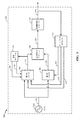
[0039]図3は、基準クロック4倍器160を例証するブロック図300である。基準クロック4倍器160は、第1のバッファ304、第2のバッファ306、組み合わせモジュール308、周波数2倍化モジュール310、フィードバックモジュール312、および遅延モジュール314を含み得る。基準クロック4倍器160はさらに、電圧制御発振器214のような発振器を含む。
[0039] FIG. 3 is a block diagram 300 illustrating a
[0040]図3を参照すれば、発振器(たとえば、シングルエンド電圧制御発振器(VCO))214は、正弦波信号320を第1のバッファ304および第2のバッファ306に出力する。正弦波信号320は、第1のクロック周波数(たとえば、基準クロック周波数)にしたがって出力され得る。
Referring to FIG. 3, an oscillator (eg, a single-ended voltage controlled oscillator (VCO)) 214 outputs a
[0041]第1のバッファ304は、正弦波信号320を受け取り、正弦波信号320に基づいて、25%のデューティサイクルを有する第1のデジタル信号を生成する。次に、第1のバッファ304は、25%のデューティサイクルを有する第1のデジタル信号324を、組み合わせモジュール308に出力する。第2のバッファ306は、正弦波信号320を受け取り、正弦波信号320に基づいて、25%のデューティサイクルを有する第2のデジタル信号を生成する。次に、第2のバッファ306は、25%のデューティサイクルを有する第2のデジタル信号326を、組み合わせモジュール308に出力する。一つの態様において、第1のバッファ304および第2のバッファ306は、25%のデューティサイクルを有するデジタル信号を生成するために、電圧しきい値がスキューされるインバータである。さらなる態様において、第1のバッファ304は、NMOSデュアルエッジスキューバッファであり得、第2のバッファ306は、PMOSスキューバッファであり得る。
[0041] The
[0042]1つの態様において、第1のバッファ304は、第1のセクションおよび第2のセクションを含む。従って、第1のセクションおよび第2のセクションのアクティブ状態は、遅延モジュール314によって制御され得る。例えば、遅延モジュール314は、第1のデジタル信号324を受け取り、第1のデジタル信号324に基づいて、第1の遅延を決定し得る。次に、遅延モジュール314は、第1の遅延に基づいて、第1のセクションに、第1のイネーブル制御信号338を送ることによって、第1のセクションのアクティブ状態を制御し得る。別の例において、遅延モジュール314は、第1のデジタル信号324に基づいて、第2の遅延を決定し得る。その後、遅延モジュール314は、第2の遅延に基づいて、第2のセクションに、第2のイネーブル制御信号340を送ることによって、第2のセクションのアクティブ状態を制御し得る。
[0042] In one aspect, the
[0043]組み合わせモジュール308は、第1のデジタル信号324および第2のデジタル信号326を受け取り、50%のデューティサイクル、および第1のクロック周波数の2倍である(2倍クロック)第2のクロック周波数を有する組み合わされたデジタル信号を生成するために、信号を組み合わせる。次に、組み合わせモジュール308は、組み合わされたデジタル信号328を周波数2倍化モジュール310に出力する。1つの態様において、組み合わせモジュール308は、1サイクルの間に最小位相ノイズ劣化を伴う4つのクリーンエッジ(たとえば、高い完全性を持った立ち上がりおよび/または立ち下がりエッジ)を有するように、組み合わされたデジタル信号を生成する。次に、4つのクリーンエッジは、周波数2倍化モジュール310に入力され得る。
[0043] The
[0044]1つの態様において、組み合わせモジュール308は、以下の動作にしたがって組み合わされたデジタル信号328を生成するために、第1のデジタル信号324および第2のデジタル信号326を組み合わせる、排他的論理和(XOR)ゲートとしてインプリメントされ得る。組み合わせモジュール308は、第1の入力として、第1のバッファ304から第1のデジタル信号324を受け取る。次に、組み合わせモジュール308は、第2の入力として、第2のバッファ306から第2のデジタル信号326を受け取る。その後、組み合わせモジュール308は、第1の入力および第2の入力を使用して、排他的論理和演算を実行し、組み合わされたデジタル信号328として他的論理和演算の結果を出力し得る。XORゲートは組み合わせモジュール308に関して説明されるが、本開示は、それに限定されない。例えば、組み合わせモジュール308はまた、XORゲートの代わりに、ORゲートとしてインプリメントされ得る。
[0044] In one aspect, the
[0045]周波数2倍化モジュール310は、組み合わされたデジタル信号328(たとえば、4つのクリーンエッジ)を受け取り、第1のクロック周波数の4倍の周波数(4倍クロック)である第3のクロック周波数を有する出力信号を生成するために、組み合わされたデジタル信号328の第2のクロック周波数を2倍化する。次に、周波数2倍化モジュール310は、出力信号330を、(TX PLL272を介して)TX周波数シンセサイザ270、および/または、(RX PLL282を介して)RX周波数シンセサイザ280、のようなトランシーバ218の様々なモジュールに出力し得る。
[0045] The
[0046]1つの態様において、周波数2倍化モジュール310は、以下の動作にしたがって出力信号330を生成するために、組み合わされたデジタル信号328の第2のクロック周波数を2倍化する、2倍器としてインプリメントされ得る。最初に、周波数2倍化モジュール310は、組み合わせモジュール308から組み合わされたデジタル信号328を受け取る。その後、周波数2倍化モジュール310は、(たとえば、XORゲートを介して)組み合わされたデジタル信号328を第1の入力として、および、組み合わされたデジタル信号328の遅延バージョンを第2の入力として排他的論理和演算を実行する。次に、周波数2倍化モジュール310は、出力信号330として、排他的論理和演算の結果を出力する。
[0046] In one aspect, the
[0047]フィードバックモジュール312は、出力信号330を受け取る。出力信号330に基づいて、フィードバックモジュール312は、第1のバッファ304を駆動するために、第1の制御電圧332および第2の制御電圧334を生成する。フィードバックモジュール312はまた、第2のバッファ306を駆動するために、出力信号330に基づいて、第3の制御電圧336を生成する。フィードバックモジュール312は、第1の制御電圧332および第2の制御電圧334を第1のバッファ304に出力し、第3の制御電圧336を第2のバッファ306に出力する。1つの態様において、第1の制御電圧332は、第1のバッファ304が第1のデジタル信号324の立ち上がりエッジを制御することを容易にする、第1のバッファ304の第1の電圧しきい値を制御/スキューする。さらなる態様において、第2の制御電圧334は、第1のバッファ304が第1のデジタル信号324の立ち下がりエッジを制御することを容易にする、第1のバッファ304の第2の電圧しきい値を制御/スキューする。別の態様において、第3の制御電圧336は、第2のバッファ306が第2のデジタル信号326の立ち上がりエッジを制御することを容易にする、第2のバッファ306の電圧しきい値を制御/スキューする。
[0047] The
[0048]第1のバッファ304に提供される第1の制御電圧332および第2の制御電圧334、および第2のバッファ306に提供される第3の制御電圧336は、50%のデューティサイクル信号328を出力する組み合わせモジュール308の能力を保証する。すなわち、フィードバックモジュール312によって提供される制御電圧は、1サイクルの間に4つのクリーンエッジを伴うデジタル信号を生成する組み合わせモジュール308の能力を保証する。それに応じて、(4つのクリーンエッジを伴うデジタル信号)50%のデューティサイクル信号328は、4倍クロックを有するスパーの無い(spur-free)出力信号330を出力する周波数2倍化モジュール310の能力を保証する。4倍クロックを有するスパーの無い出力信号330は、(TX PLL272を介して)TX周波数シンセサイザ270に、および/または、(RX PLL282を介して)RX周波数シンセサイザ280に入力されたとき、PN性能を改善する。
[0048] The
[0049]図4は、図3のフィードバックモジュール312を例証する図400である。図3および4を参照すれば、フィードバックモジュール312は、位相周波数検知器402、デマルチプレクサ408、第1のデューティサイクル補正(DCC)モジュール410、第2のDCCモジュール412、および第3のDCCモジュール336を含み得る。
[0049] FIG. 4 is a diagram 400 illustrating the
[0050]位相周波数検知器402は、周波数2倍化モジュール310から出力信号330を受け取り、出力信号330のエッジに基づいて、アップ/ダウン信号を生成する。1つの態様において、位相周波数検知器402は、4倍クロックを有する出力信号330のレプリカを生成し、出力信号330の全エッジ変動を平均化するように構成された位相ロックループ(PLL)の一部であり得る。PLLは、チャージポンプおよびローパスフィルタ(CPおよびPF)406および発振器404を含み得る。アップ/ダウン信号416は、デマルチプレクサ408および/またはCPおよびLPF406に出力され得る。
[0050] The
[0051]デマルチプレクサ408は、アップ/ダウン信号416を受け取り、出力信号330のエッジに対応するアップ/ダウン信号416のパルスを分離する。デマルチプレクサ408は、第1の分離されたパルス418を第1のDCCモジュール410に、第2の分離されたパルス420を第2のDCCモジュール412に、および第3の分離されたパルス422を第3のDCCモジュール414に出力する。第1のDCCモジュール410は、第1の分離されたパルス418に基づいて、第1の制御電圧332を生成し、出力する。第2のDCCモジュール412は、第2の分離されたパルス420に基づいて、第2の制御電圧334を生成し、出力する。第3のDCCモジュール414は、第3の分離されたパルス422に基づいて、第3の制御電圧336を生成し、出力する。
[0051]
[0052]1つの態様において、上記に説明された何れのDCCモジュール410、412、または414も、インバータ、第1のローパスフィルタ(LPF)、第2のLPF、および演算増幅器を含み得る。インバータは、反転パルスを生成するために、分離されたパルス(たとえば、第1の分離されたパルス418、第2の分離されたパルス420、または第3の分離されたパルス422)を反転し得る。第1のLPFは、反転パルスの平均を生成する。第2のLPFは、分離されたパルスの平均を生成する。演算増幅器は、非反転入力を介して反転パルスの平均を受け取り、反転入力を介して、分離されたパルスの平均を受け取る。演算増幅器はさらに、反転パルスの平均および分離されたパルスの平均間の電圧の差を決定し、制御電圧(たとえば、第1の制御電圧332、第2の制御電圧334、または第3の制御電圧336)を生成するために、電圧差を増幅する。上記で言及した特定の要素を含めるためにDCCモジュールが説明されたが、本開示にしたがって、クロックデューティサイクルを検知することの可能ないかなるタイプのDCCフィードバックシステムも使用し得るので、本開示のDCCモジュールは、これに限定されない。
[0052] In one aspect, any of the
[0053]図5は、図3の遅延モジュール314に結合された第1のバッファ304を例証する、例となる図式的回路図500である。図3および5を参照すれば、第1のバッファ304は、フィードバックモジュール312から受け取られた第1の制御電圧332にしたがって、第1のバッファ304から出力された第1のデジタル信号324の立ち上がりエッジを制御するための第1のセクションを含む。第1のバッファ304はまた、フィードバックモジュール312から受け取られた第2の制御電圧334にしたがって、第1のバッファ304から出力された第1のデジタル信号324の立ち下がりエッジを制御するための第2のセクションを含む。遅延モジュール314は、第1のセクションおよび第2のセクション間のスイッチングが第1のデジタル信号324の出力に影響を与えないように、遅延を調整するように動作される。
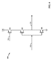
[0053] FIG. 5 is an exemplary schematic circuit diagram 500 illustrating the
[0054]第1のバッファ304の第1のセクションは、第1のトランジスタ502、第2のトランジスタ504、第3のトランジスタ506、および第4のトランジスタ508を含む。第1のトランジスタ502のゲートは、正弦波信号320を出力するVCO214の出力に結合される。第1のトランジスタ502のドレインは、第2のトランジスタ504のドレイン、組み合わせモジュール308の第1の入力、および遅延モジュール314の入力に結合される。第1のトランジスタ502のソースは、電圧源Vddに結合される。
[0054] The first section of the
[0055]第2のトランジスタ504のゲートは、正弦波信号320を出力するVCO214の出力に結合される。第2のトランジスタ504のドレインは、第1のトランジスタ502のドレインに結合される。第2のトランジスタ504のソースは、第3のトランジスタ506のドレインに結合される。
[0055] The gate of the
[0056]第3のトランジスタ506のゲートは、第1の制御電圧332を出力するフィードバックモジュール312の第1の出力に結合される。第3のトランジスタ506のドレインは、第2のトランジスタ504のソースに結合される。第3のトランジスタ506のソースは、第4のトランジスタ508のドレインに結合される。
[0056] The gate of the
[0057]第4のトランジスタ508のゲートは、遅延モジュール314の第1の出力338に結合される。第4のトランジスタ508のドレインは、第3のトランジスタ506のソースに結合される。第4のトランジスタ508のソースは、接地ノードに結合される。
[0057] The gate of the
[0058]第1のバッファ304の第2のセクションは、第1のトランジスタ502、第5のトランジスタ510、第6のトランジスタ512、および第7のトランジスタ514を含む。第1のトランジスタ502のドレインは、第5のトランジスタ510のドレインに結合される。
[0058] The second section of the
[0059]第5のトランジスタのゲートは、正弦波信号320を出力するVCO214の出力に結合される。第5のトランジスタ510のドレインは、第1のトランジスタ502のドレインに結合される。第5のトランジスタ510のソースは、第6のトランジスタ512のドレインに結合される。
[0059] The gate of the fifth transistor is coupled to the output of the
[0060]第6のトランジスタ512のゲートは、第2の制御電圧334を出力するフィードバックモジュール312の第2の出力に結合される。第6のトランジスタ512のドレインは、第5のランジスタ510のソースに結合される。第6のトランジスタ512のソースは、第7のランジスタ514のドレインに結合される。
[0060] The gate of the
[0061]第7のトランジスタ514のゲートは、遅延モジュール314の第2の出力340に結合される。第7のトランジスタ514のドレインは、第6のトランジスタ512のソースに結合される。第7のトランジスタ514のソースは、接地ノードに結合される。
[0061] The gate of the
[0062]1つの態様において、遅延モジュール314は、第1のセクションのアクティブ状態を制御し得る。例えば、遅延モジュール314は、第1のバッファ304によって出力される第1のデジタル信号324を受け取り、受け取られた第1のデジタル信号324に基づいて、第1の遅延を決定し得る。その後、遅延モジュール314は、第1の遅延に基づいて、第4のトランジスタ508のゲートに、第1のイネーブル制御信号338を送ることによって、第1のセクションをアクティブ化し得る。
[0062] In one aspect, the
[0063]別の態様において、遅延モジュール314は、第1のバッファ304の第2のセクションのアクティブ状態を制御し得る。例えば、遅延モジュール314は、受け取られた第1のデジタル信号324に基づいて、第2の遅延を決定し、その後、第2の遅延に基づいて、第2のイネーブル制御信号340を第7のトランジスタ514のゲートに送ることによって、第2のセクションをアクティブ化し得る。
[0063] In another aspect, the
[0064]図6は、図3の第2のバッファ306を例証する、例となる図式的回路図600である。図3および6を参照すれば、第2のバッファ306は、フィードバックモジュール312から受け取られた第3の制御電圧336にしたがって、出力された第2のデジタル信号326の立ち上がりエッジを制御する。第2のバッファ306は、第8のトランジスタ602、第9のトランジスタ604、および第10のトランジスタ606を含む。
[0064] FIG. 6 is an exemplary schematic circuit diagram 600 illustrating the
[0065]第8のトランジスタ602のゲートは、第3の制御電圧336を出力するフィードバックモジュール312の第3の出力に結合される。第8のトランジスタ602のドレインは第9のトランジスタ604のソースに結合される。第8のトランジスタ602のソースは、電圧源Vddに結合される。
[0065] The gate of the eighth transistor 602 is coupled to a third output of the
[0066]第9のトランジスタ604のゲートは、正弦波信号320を出力するVCO214の出力に結合される。第9のトランジスタ604のソースは、第8のトランジスタ602のドレインに結合される。第9のトランジスタ604のドレインは、第10のトランジスタ606のドレインおよび組み合わせモジュール308の第2の入力に結合される。
[0066] The gate of the ninth transistor 604 is coupled to the output of the
[0067]第10のトランジスタ606のゲートは、正弦波信号320を出力するVCO214の出力に結合される。第10のトランジスタ606のドレインは、第9のトランジスタ604のドレインに結合される。第10のトランジスタ606のソースは、接地ノードに結合される。
[0067] The gate of the
[0068]図7は、クロック周波数を4倍化する方法のフローチャート700である。方法は、発振器214、第1のバッファ304、第2のバッファ306、組み合わせモジュール308、周波数2倍化モジュール310、フィードバックモジュール312、または遅延モジュール314の内の1つまたは複数を介して、装置(たとえば、基準クロック4倍器160)によって実行され得る。
[0068] FIG. 7 is a
[0069]ブロック702において、装置は、第1のクロック周波数にしたがって、発振器214を介して、正弦波信号を出力する。ブロック704において、装置は、正弦波信号に基づいて、第1のバッファ304を介して、25%のデューティサイクルを有する第1のデジタル信号を生成する。
[0069] In
[0070]ブロック706において、装置は、遅延モジュール314を介して、第1のバッファ304の第1のセクションおよび第2のセクションのアクティブ状態を制御する。ブロック708において、装置は、第2のバッファ306を介して、正弦波信号に基づいて、25%のデューティサイクルを有する第2のデジタル信号を生成する。
[0070] In
[0071]ブロック710において、装置は、組み合わせモジュール308を介して、50%のデューティサイクルを有する組み合わされたデジタル信号を生成するために、第1のデジタル信号および第2のデジタル信号を組み合わせる。組み合わされたデジタル信号は、第1のクロック周波数の2倍である第2のクロック周波数を有する。1つの態様において、組み合わせモジュール308は、第1のバッファ304から第1の入力として第1のデジタル信号を受け取ること、第2のバッファ306から第2の入力として第2のデジタル信号を受け取ること、第1の入力および第2の入力を使用して排他的論理和演算を実行すること、および組み合わされたデジタル信号として排他的論理和演算の結果を出力することとによって、組み合わされたデジタル信号を生成する。
[0071] At
[0072]ブロック712において、装置は、第1のクロック周波数の4倍である第3のクロック周波数を有する出力信号を生成するために、周波数2倍化モジュール310を介して、組み合わされたデジタル信号の第2のクロック周波数を2倍化する。1つの態様において、周波数2倍化モジュール310は、組み合わせモジュール308から組み合わされたデジタル信号を受け取ること、組み合わされたデジタル信号を第1の入力として、および組み合わされたデジタル信号の遅延されたバージョンを第2の入力として使用して、排他的論理和演算を実行すること、および出力信号として排他的論理和演算の結果を出力することとによって、出力信号を生成する。
[0072] At
[0073]ブロック714において、装置は、フィードバックモジュール312を介して、出力信号に基づいて、第1のバッファ304のための第1の制御電圧および第2の制御電圧と、第2のバッファ306のための第3の制御電圧とを生成する。第1の制御電圧は、第1のバッファ304が第1のデジタル信号の立ち上がりエッジを制御することを容易にする、第1のバッファ304の第1のしきい値を制御する。第2の制御電圧は、第1のバッファ304が第1のデジタル信号の立ち下がりエッジを制御することを容易にする、第1のバッファ304の第2のしきい値を制御する。第3の制御電圧は、第2のバッファ306が第2のデジタル信号の立ち上がりエッジを制御することを容易にする、第2のバッファ306のしきい値を制御する。
[0073] In
[0074]1つの態様において、装置は、以下の動作にしたがって、第1の制御電圧、第2の制御電圧、および第3の制御電圧を生成する。装置は、位相周波数検出器(PFD)を介して、出力信号のエッジに基づいて、アップ/ダウンパルス信号を生成する。次に、装置は、デマルチプレクサを介して、出力信号のエッジに対応して、アップ/ダウンパルス信号のパルスをそれぞれ分離する。その後、装置は、第1のデューティサイクル補正(DCC)モジュールを介して、第1の分離されたパルスに基づいて、第1の制御電圧を、第2のDCCモジュールを介して、第2の分離されたパルスに基づいて、第2の制御電圧を、および第3のDCCモジュールを介して、第3の分離されたパルスに基づいて、第3の制御電圧を生成する。 [0074] In one aspect, the apparatus generates a first control voltage, a second control voltage, and a third control voltage according to the following operations. The device generates an up / down pulse signal based on the edge of the output signal via a phase frequency detector (PFD). Next, the device separates each pulse of the up / down pulse signal through the demultiplexer corresponding to the edge of the output signal. Thereafter, the device sends a first control voltage to the second isolation via the second DCC module based on the first isolated pulse via the first duty cycle correction (DCC) module. A second control voltage is generated based on the generated pulse, and a third control voltage is generated based on the third separated pulse via the third DCC module.
[0075]1つの態様において、第1のバッファ304は、第1のセクションおよび第2のセクションを備える。第1のセクションは、第1のトランジスタ、第2のトランジスタ、第3のトランジスタ、および第4のトランジスタを含む。第1のトランジスタのソースは、電圧源に結合される。第1のトランジスタのゲートは、正弦波信号を出力する発振器214の出力に結合される。第1のトランジスタのドレインは、第2のトランジスタのドレイン、組み合わせモジュール308の第1の入力、および遅延モジュール314の入力に結合される。第2のトランジスタのゲートは、正弦波信号を出力する発振器214の出力に結合される。第2のトランジスタのドレインは、第1のトランジスタのドレインに結合される。第2のトランジスタのソースは、第3のトランジスタのドレインに結合される。第3のトランジスタのゲートは、第1の制御電圧を出力するフィードバックモジュール312の第1の出力に結合される。第3のトランジスタのドレインは、第2のトランジスタのソースに結合される。第3のトランジスタのソースは、第4のトランジスタのドレインに結合される。第4のトランジスタのゲートは、遅延モジュール314の第1の出力に結合される。第4のトランジスタのドレインは、第3のトランジスタのソースに結合される。第4のトランジスタのソースは、接地ノードに結合される。
[0075] In one aspect, the
[0076]第2のセクションは、第1のトランジスタ、第5のトランジスタ、第6のトランジスタ、および第7のトランジスタを含む。第1のトランジスタのドレインは、第5のトランジスタのドレインに結合される。第5のトランジスタのゲートは、正弦波信号を出力する発振器214の出力に結合される。第5のトランジスタのドレインは、第1のトランジスタのドレインに結合される。第5のトランジスタのソースは、第6のトランジスタのドレインに結合される。第6のトランジスタのゲートは、第2の制御電圧を出力するフィードバックモジュール312の第2の出力に結合される。第6のトランジスタのドレインは、第5のトランジスタのソースに結合される。第6のトランジスタのソースは、第7のトランジスタのドレインに結合される。第7のトランジスタのゲートは、遅延モジュール314の第2の出力に結合される。第7のトランジスタのドレインは、第6のトランジスタのソースに結合される。第7のトランジスタのソースは、接地ノードに結合される。
[0076] The second section includes a first transistor, a fifth transistor, a sixth transistor, and a seventh transistor. The drain of the first transistor is coupled to the drain of the fifth transistor. The gate of the fifth transistor is coupled to the output of an
[0077]1つの態様において、遅延モジュール314は、第1のバッファ304から出力された第1のデジタル信号を受け取ること、受け取られた第1のデジタル信号に基づいて、第1の遅延を決定すること、および第1の遅延に基づいて、第4のトランジスタのゲートに第1のイネーブル制御信号を送ることにより第1のセクションをアクティブ化することとによって、第1のバッファ304の第1のセクションのアクティブ状態を制御する。さらなる態様において、遅延モジュール314は、受け取られた第1のデジタル信号に基づいて、第2の遅延を決定すること、および第2の遅延に基づいて、第2のイネーブル制御信号を第7のトランジスタのゲートに送ることにより第2のセクションをアクティブ化することとによって、第1のバッファ304の第2のセクションのアクティブ状態を制御する。
[0077] In one aspect, the
[0078]1つの態様において、第2のバッファ306は、第8のトランジスタ、第9のトランジスタ、および第10のトランジスタを含む。第8のトランジスタのソースは、電圧源に結合される。第8のトランジスタのゲートは、第3の制御電圧を出力するフィードバックモジュール312の第3の出力に結合される。第8のトランジスタのドレインは、第9のトランジスタのソースに結合される。第9のトランジスタのゲートは、正弦波信号を出力する発振器214の出力に結合される。第9のトランジスタのソースは、第8のトランジスタのドレインに結合される。第9のトランジスタのドレインは、第10のトランジスタのドレインおよび組み合わせモジュール308の第2の入力に結合される。第10のトランジスタのゲートは、正弦波信号を出力する発振器214の出力に結合される。第10のトランジスタのドレインは、第9のトランジスタのドレインに結合される。第10のトランジスタのソースは、接地ノードに結合される。
[0078] In one aspect, the
[0079]図3を再び参照すれば、装置(たとえば、基準クロック4倍器160)は、発振器214、第1のバッファ304、第2のバッファ306、組み合わせモジュール308、周波数2倍化モジュール310、フィードバックモジュール312、および遅延モジュール314を含み得る。装置は、第1のクロック周波数にしたがって、正弦波信号を出力するための手段を含む。装置はまた、正弦波信号に基づいて25%のデューティサイクを有する第1のデジタル信号を生成するための手段を含む。装置はさらに、正弦波信号に基づいて、25%のデューティサイクルを有する第2のデジタル信号を生成するための手段を含む。装置は、50%のデューティサイクルを有する組み合わされたデジタル信号を生成するために、第1のデジタル信号および第2のデジタル信号を組み合わせるための手段を含み、組み合わされたデジタル信号は、第1のクロック周波数の2倍である第2のクロック周波数を有する。装置はさらに、第1のクロック周波数の4倍である第3のクロック周波数を有する出力信号を生成するために、組み合わされたデジタル信号の第2のクロック周波数を2倍化するための手段を含む。装置はまた、出力信号に基づいて、第1のバッファのための第1の制御電圧および第2の制御電圧、および第2のバッファのための第3の制御電圧を生成するように構成されたフィードバックを提供するための手段を含む。装置は、第1のバッファの第1のセクションおよび第2のセクションのアクティブ状態を制御するように構成された遅延するための手段を含む。前述した手段は、発振器214、第1のバッファ304、第2のバッファ306、組み合わせモジュール308、周波数2倍化モジュール310、フィードバックモジュール312、遅延モジュール314、データプロセッサ/コントローラ210、前述の手段によって引用された機能を実行するように構成された、コンピュータ可読媒体、即ちメモリ212、および/またはコンピュータ可読媒体、即ちメモリ216の内の1つまたは複数であり得る。
[0079] Referring back to FIG. 3, the device (eg, reference clock quadrupler 160) includes an
[0080]開示されたプロセスおけるステップの特定の順序または階層は、例示的アプローチの例証であることが理解される。設計の好みに基づいて、プロセスにおけるステップの特定の順序または階層は再配置され得ることが理解される。さらに、いくつかのステップは、組み合わされ得るか、または省略され得る。添付の方法の特許請求の範囲は、サンプルの順序で様々なステップの要素を提示しており、提示された特定の順序または階層に限定されるようには意味されない。 [0080] It is understood that the specific order or hierarchy of steps in the disclosed processes is illustrative of an exemplary approach. It is understood that a specific order or hierarchy of steps in the process can be rearranged based on design preferences. In addition, some steps may be combined or omitted. The accompanying method claims present elements of the various steps in a sample order, and are not meant to be limited to the specific order or hierarchy presented.
[0081]先の説明は、いかなる当業者であっても、本明細書で説明された様々な態様を実施することを可能にするために提供される。これらの態様への様々な修正は、当業者にとって容易に明らかとなり、本明細書に定義された包括的な原理は、他の態様に適用され得る。よって、特許請求の範囲は、本明細書に差し示される態様に限定されるように意図されたものではなく、特許請求の範囲の文言と一貫する最大範囲であると認められるべきであり、ここにおいて、単数における要素の参照は、そのように明確に述べられていない限りは「1つおよび1つのみ」を意味するのではなく、むしろ「1つまたは複数」を意味するように意図される。そうでないと具体的に記載されない限り、「何らかの/いくつかの」という用語は、1つまたは複数を指す。当業者に既知の、または後に周知となる、本開示全体にわたって説明された様々な態様の要素と構造的および機能的に同等な物はすべて、参照によって本明細書に明確に組み込まれ、特許請求の範囲に包含されるよう意図される。さらに、本明細書で開示されたものが、特許請求の範囲の中に明示的に記載されているか否かに関わらず、公に捧げられることを意図していない。要素が「〜のための手段」というフレーズを使用して明確に記載されていない限り、どの請求項の要素もミーンズプラスファンクションとして解釈されるべきではない。 [0081] The previous description is provided to enable any person skilled in the art to practice the various aspects described herein. Various modifications to these aspects will be readily apparent to those skilled in the art, and the generic principles defined herein may be applied to other aspects. Thus, the claims are not intended to be limited to the embodiments presented herein, but are to be accorded the greatest scope consistent with the language of the claims, In the singular, reference to an element in the singular is not intended to mean “one and only one” unless expressly stated otherwise, but rather to mean “one or more”. . Unless otherwise specifically stated, the term “some / some” refers to one or more. All structurally and functionally equivalent to the elements of the various aspects described throughout this disclosure that are known to those skilled in the art or that will be well known later are expressly incorporated herein by reference and are It is intended to be included in the scope of Moreover, nothing disclosed in this specification is intended to be dedicated to the public regardless of whether or not explicitly stated in the claims. No claim element should be construed as a means plus function unless the element is expressly recited using the phrase “means for”.
Claims (30)
第1のクロック周波数にしたがって、正弦波信号を出力するように構成された電圧制御発振器(VCO)と、
前記正弦波信号に基づいて、25%のデューティサイクルを有する第1のデジタル信号を生成するように構成された第1のバッファと、
前記正弦波信号に基づいて、25%のデューティサイクルを有する第2のデジタル信号を生成するように構成された第2のバッファと、
50%のデューティサイクルを有する組み合わされたデジタル信号を生成するために、前記第1のデジタル信号と前記第2のデジタル信号とを組み合わせるように構成された組み合わせモジュールと、前記組み合わされたデジタル信号は、前記第1のクロック周波数の2倍である第2のクロック周波数を有し、
前記第1のクロック周波数の4倍である第3のクロック周波数を有する出力信号を生成するために、前記組み合わされたデジタル信号の前記第2のクロック周波数を2倍化するように構成された周波数2倍化モジュールと、を備える、装置。 A device for quadrupling the clock frequency,
A voltage controlled oscillator (VCO) configured to output a sinusoidal signal according to a first clock frequency;
A first buffer configured to generate a first digital signal having a 25% duty cycle based on the sinusoidal signal;
A second buffer configured to generate a second digital signal having a 25% duty cycle based on the sinusoidal signal;
A combination module configured to combine the first digital signal and the second digital signal to generate a combined digital signal having a 50% duty cycle; and A second clock frequency that is twice the first clock frequency;
A frequency configured to double the second clock frequency of the combined digital signal to produce an output signal having a third clock frequency that is four times the first clock frequency. And a doubling module.
前記第1の制御電圧は、前記第1のバッファが前記第1のデジタル信号の立ち上がりエッジを制御することを容易にする、前記第1のバッファの第1のしきい値を制御し、
前記第2の制御電圧は、前記第1のバッファが前記第1のデジタル信号の立ち下がりエッジを制御することを容易にする、前記第1のバッファの第2のしきい値を制御し、
前記第3の制御電圧は、前記第2のバッファが前記第2のデジタル信号の立ち上がりエッジを制御することを容易にする、前記第2のバッファのしきい値を制御する、請求項1に記載の装置。 Based on the output signal, configured to generate a first control voltage and a second control voltage for the first buffer, and a third control voltage for the second buffer A feedback module,
The first control voltage controls a first threshold of the first buffer that facilitates the first buffer to control a rising edge of the first digital signal;
The second control voltage controls a second threshold of the first buffer that facilitates the first buffer to control a falling edge of the first digital signal;
The third control voltage controls a threshold of the second buffer that facilitates the second buffer to control a rising edge of the second digital signal. Equipment.
前記出力信号のエッジに基づいて、アップ/ダウンパルス信号を生成するように構成された位相周波数検出器(PFD)と、
前記出力信号の前記エッジにそれぞれ対応する前記アップ/ダウンパルス信号のパルスを分離するように構成されたデマルチプレクサと、
第1の分離されたパルスに基づいて、前記第1の制御電圧を生成するように構成された第1のデューティサイクル補正(DCC)モジュールと、
第2の分離されたパルスに基づいて、前記第2の制御電圧を生成するように構成された第2のDCCモジュールと、
第3の分離されたパルスに基づいて、前記第3の制御電圧を生成するように構成された第3のDCCモジュールと、を備える、請求項2に記載の装置。 The feedback module is
A phase frequency detector (PFD) configured to generate an up / down pulse signal based on an edge of the output signal;
A demultiplexer configured to separate pulses of the up / down pulse signal corresponding respectively to the edges of the output signal;
A first duty cycle correction (DCC) module configured to generate the first control voltage based on a first separated pulse;
A second DCC module configured to generate the second control voltage based on a second separated pulse;
The apparatus of claim 2, comprising: a third DCC module configured to generate the third control voltage based on a third separated pulse.
前記第1のセクションは、第1のトランジスタ、第2のトランジスタ、第3のトランジスタ、および第4のトランジスタを備え、
前記第1のトランジスタのゲートは、前記正弦波信号を出力する前記VCOの出力に結合され、前記第1のトランジスタのドレインは、前記第2のトランジスタのドレイン、前記組み合わせモジュールの第1の入力、および遅延モジュールの入力に結合され、
前記第2のトランジスタのゲートは、前記正弦波信号を出力する前記VCOの前記出力に結合され、前記第2のトランジスタの前記ドレインは、前記第1のトランジスタの前記ドレインに結合され、前記第2のトランジスタのソースは、前記第3のトランジスタのドレインに結合され、
前記第3のトランジスタのゲートは、前記第1の制御電圧を出力する前記フィードバックモジュールの第1の出力に結合され、前記第3のトランジスタの前記ドレインは、前記第2のトランジスタの前記ソースに結合され、前記第3のトランジスタのソースは、前記第4のトランジスタのドレインに結合され、
前記第4のトランジスタのゲートは、前記遅延モジュールの第1の出力に結合され、前記第4のトランジスタの前記ドレインは、前記第3のトランジスタの前記ソースに結合される、請求項2に記載の装置。 The first buffer comprises a first section and a second section;
The first section comprises a first transistor, a second transistor, a third transistor, and a fourth transistor;
The gate of the first transistor is coupled to the output of the VCO that outputs the sinusoidal signal, the drain of the first transistor is the drain of the second transistor, the first input of the combination module, And coupled to the input of the delay module,
The gate of the second transistor is coupled to the output of the VCO that outputs the sinusoidal signal, the drain of the second transistor is coupled to the drain of the first transistor, and the second transistor The source of the transistor is coupled to the drain of the third transistor;
The gate of the third transistor is coupled to a first output of the feedback module that outputs the first control voltage, and the drain of the third transistor is coupled to the source of the second transistor. And the source of the third transistor is coupled to the drain of the fourth transistor;
The gate of the fourth transistor is coupled to a first output of the delay module, and the drain of the fourth transistor is coupled to the source of the third transistor. apparatus.
前記第1のトランジスタの前記ドレインは、前記第5のトランジスタのドレインに結合され、
前記第5のトランジスタのゲートは、前記正弦波信号を出力する前記VCOの前記出力に結合され、前記第5のトランジスタの前記ドレインは、前記第1のトランジスタの前記ドレインに結合され、前記第5のトランジスタのソースは、前記第6のトランジスタのドレインに結合され、
前記第6のトランジスタのゲートは、前記第2の制御電圧を出力する前記フィードバックモジュールの第2の出力に結合され、前記第6のトランジスタの前記ドレインは、前記第5のトランジスタの前記ソースに結合され、前記第6のトランジスタのソースは、前記第7のトランジスタのドレインに結合され、
前記第7のトランジスタのゲートは、前記遅延モジュールの第2の出力に結合され、前記第7のトランジスタの前記ドレインは、前記第6のトランジスタの前記ソースに結合される、請求項4に記載の装置。 The second section comprises the first transistor, the fifth transistor, the sixth transistor, and the seventh transistor;
The drain of the first transistor is coupled to the drain of the fifth transistor;
The gate of the fifth transistor is coupled to the output of the VCO that outputs the sine wave signal, the drain of the fifth transistor is coupled to the drain of the first transistor, and the fifth transistor The source of the transistor is coupled to the drain of the sixth transistor;
The gate of the sixth transistor is coupled to a second output of the feedback module that outputs the second control voltage, and the drain of the sixth transistor is coupled to the source of the fifth transistor. The source of the sixth transistor is coupled to the drain of the seventh transistor;
The gate of the seventh transistor is coupled to a second output of the delay module, and the drain of the seventh transistor is coupled to the source of the sixth transistor. apparatus.
前記第4のトランジスタのソースおよび前記第7のトランジスタのソースは、接地ノードに結合される、請求項5に記載の装置。 The source of the first transistor is coupled to a voltage source;
The apparatus of claim 5, wherein a source of the fourth transistor and a source of the seventh transistor are coupled to a ground node.
前記第1のバッファから出力された前記第1のデジタル信号を受け取ることと、
前記受け取られた第1のデジタル信号に基づいて、第1の遅延を決定することと、
前記第1の遅延に基づいて、第1のイネーブル制御信号を前記第4のトランジスタの前記ゲートに送ることによって前記第1のセクションをアクティブ化することと、
前記受け取られた第1のデジタル信号に基づいて、第2の遅延を決定することと、
前記第2の遅延に基づいて、第2のイネーブル制御信号を前記第7のトランジスタの前記ゲートに送ることにより前記第2のセクションをアクティブ化することとによって、前記第1のセクションおよび前記第2のセクションのアクティブ状態を制御するように構成される、請求項5に記載の装置。 The delay module is
Receiving the first digital signal output from the first buffer;
Determining a first delay based on the received first digital signal;
Activating the first section based on the first delay by sending a first enable control signal to the gate of the fourth transistor;
Determining a second delay based on the received first digital signal;
Based on the second delay, activating the second section by sending a second enable control signal to the gate of the seventh transistor, thereby enabling the first section and the second section to be activated. The apparatus of claim 5, wherein the apparatus is configured to control an active state of a section of the.
前記第8のトランジスタのゲートは、前記第3の制御電圧を出力する前記フィードバックモジュールの第3の出力に結合され、前記第8のトランジスタのドレインは、前記第9のトランジスタのソースに結合され、
前記第9のトランジスタのゲートは、前記正弦波信号を出力する前記VCOの前記出力に結合され、前記第9のトランジスタの前記ソースは、前記第8のトランジスタの前記ドレインに結合され、前記第9のトランジスタのドレインは、前記第10のトランジスタのドレインおよび前記組み合わせモジュールの第2の入力に結合され、
前記第10のトランジスタのゲートは、前記正弦波信号を出力する前記VCOの前記出力に結合され、前記第10のトランジスタの前記ドレインは、前記第9のトランジスタの前記ドレインに結合される、請求項5に記載の装置。 The second buffer includes an eighth transistor, a ninth transistor, and a tenth transistor,
A gate of the eighth transistor is coupled to a third output of the feedback module that outputs the third control voltage; a drain of the eighth transistor is coupled to a source of the ninth transistor;
The gate of the ninth transistor is coupled to the output of the VCO that outputs the sinusoidal signal, the source of the ninth transistor is coupled to the drain of the eighth transistor, and the ninth transistor A drain of the transistor coupled to a drain of the tenth transistor and a second input of the combination module;
The gate of the tenth transistor is coupled to the output of the VCO that outputs the sinusoidal signal, and the drain of the tenth transistor is coupled to the drain of the ninth transistor. 5. The apparatus according to 5.
前記第10のトランジスタのソースは、接地ノードに結合される、請求項8に記載の装置。 The source of the eighth transistor is coupled to a voltage source;
The apparatus of claim 8, wherein a source of the tenth transistor is coupled to a ground node.
前記第1のデジタル信号を前記第1のバッファから第1の入力として受け取ることと、
前記第2のデジタル信号を前記第2のバッファから第2の入力として受け取ることと、
前記第1の入力および前記第2の入力を使用して、排他的論理和演算を実行することと、
前記排他的論理和演算の結果を前記組み合わせされたデジタル信号として出力することとによって、前記組み合わされたデジタル信号を生成するために、前記第1のデジタル信号と前記第2のデジタル信号とを組み合わせるように構成される、請求項1に記載の装置。 The combination module is
Receiving the first digital signal from the first buffer as a first input;
Receiving the second digital signal from the second buffer as a second input;
Performing an exclusive OR operation using the first input and the second input;
Combining the first digital signal and the second digital signal to generate the combined digital signal by outputting the result of the exclusive OR operation as the combined digital signal; The apparatus of claim 1, configured as follows.
前記組み合わされたデジタル信号を前記組み合わせモジュールから受け取ることと、
第1の入力として前記組み合わされたデジタル信号と、第2の入力として前記組み合わされたデジタル信号の遅延されたバージョンとを使用して、排他的論理和演算を実行することと、
前記排他的論理和演算の結果を前記出力信号として出力することとによって、前記出力信号を生成するために、前記組み合わされたデジタル信号の前記第2のクロック周波数を2倍化するように構成される、請求項1に記載の装置。 The frequency doubling module includes:
Receiving the combined digital signal from the combination module;
Performing an exclusive OR operation using the combined digital signal as a first input and a delayed version of the combined digital signal as a second input;
The second clock frequency of the combined digital signal is doubled to produce the output signal by outputting the result of the exclusive OR operation as the output signal. The apparatus of claim 1.
電圧制御発振器(VCO)を介して、第1のクロック周波数にしたがって、正弦波信号を出力することと、
第1のバッファを介して、前記正弦波信号に基づいて、25%のデューティサイクルを有する第1のデジタル信号を生成することと、
第2のバッファを介して、前記正弦波信号に基づいて、25%のデューティサイクルを有する第2のデジタル信号を生成することと、
組み合わせモジュールを介して、50%のデューティサイクルを有する組み合わされたデジタル信号を生成するために、前記第1のデジタル信号と前記第2のデジタル信号とを組み合わせることと、前記組み合わされたデジタル信号は、前記第1のクロック周波数の2倍である第2のクロック周波数を有し、
周波数2倍化モジュールを介して、前記第1のクロック周波数の4倍である第3のクロック周波数を有する出力信号を生成するために、前記組み合わされたデジタル信号の前記第2のクロック周波数を2倍化することと、を備える、方法。 A method of quadrupling the clock frequency,
Outputting a sinusoidal signal according to a first clock frequency via a voltage controlled oscillator (VCO);
Generating a first digital signal having a 25% duty cycle based on the sinusoidal signal via a first buffer;
Generating a second digital signal having a duty cycle of 25% based on the sinusoidal signal via a second buffer;
Combining the first digital signal and the second digital signal to produce a combined digital signal having a 50% duty cycle via a combination module, the combined digital signal is A second clock frequency that is twice the first clock frequency;
To generate an output signal having a third clock frequency that is four times the first clock frequency via a frequency doubling module, the second clock frequency of the combined digital signal is 2 Doubling the method.
前記第1の制御電圧は、前記第1のバッファが前記第1のデジタル信号の立ち上がりエッジを制御することを容易にする、前記第1のバッファの第1のしきい値を制御し、
前記第2の制御電圧は、前記第1のバッファが前記第1のデジタル信号の立ち下がりエッジを制御することを容易にする、前記第1のバッファの第2のしきい値を制御し、
前記第3の制御電圧は、前記第2のバッファが前記第2のデジタル信号の立ち上がりエッジを制御することを容易にする、前記第2のバッファのしきい値を制御する、請求項12に記載の方法。 Generate a first control voltage and a second control voltage for the first buffer and a third control voltage for the second buffer based on the output signal via a feedback module More to do,
The first control voltage controls a first threshold of the first buffer that facilitates the first buffer to control a rising edge of the first digital signal;
The second control voltage controls a second threshold of the first buffer that facilitates the first buffer to control a falling edge of the first digital signal;
13. The third control voltage controls a threshold of the second buffer that facilitates the second buffer to control a rising edge of the second digital signal. the method of.
位相周波数検出器(PFD)を介して、前記出力信号のエッジに基づいて、アップ/ダウンパルス信号を生成することと、
デマルチプレクサを介して、前記出力信号の前記エッジにそれぞれ対応する前記アップ/ダウンパルス信号のパルスを分離することと、
第1のデューティサイクル補正(DCC)モジュールを介して、第1の分離されたパルスに基づいて、前記第1の制御電圧を生成することと、
第2のDCCモジュールを介して、第2の分離されたパルスに基づいて、前記第2の制御電圧を生成することと、
第3のDCCモジュールを介して、第3の分離されたパルスに基づいて、前記第3の制御電圧を生成することと、を備える、請求項13に記載の方法。 Generating the first control voltage, the second control voltage, and the third control voltage;
Generating an up / down pulse signal based on an edge of the output signal via a phase frequency detector (PFD);
Separating pulses of the up / down pulse signal corresponding respectively to the edges of the output signal via a demultiplexer;
Generating the first control voltage based on a first isolated pulse via a first duty cycle correction (DCC) module;
Generating the second control voltage based on a second separated pulse via a second DCC module;
The method of claim 13, comprising generating the third control voltage based on a third separated pulse via a third DCC module.
前記第1のセクションは、第1のトランジスタ、第2のトランジスタ、第3のトランジスタ、および第4のトランジスタを備え、
前記第1のトランジスタのゲートは、前記正弦波信号を出力する前記VCOの出力に結合され、前記第1のトランジスタのドレインは、前記第2のトランジスタのドレイン、前記組み合わせモジュールの第1の入力、および遅延モジュールの入力に結合され、
前記第2のトランジスタのゲートは、前記正弦波信号を出力する前記VCOの前記出力に結合され、前記第2のトランジスタの前記ドレインは、前記第1のトランジスタの前記ドレインに結合され、前記第2のトランジスタのソースは、前記第3のトランジスタのドレインに結合され、
前記第3のトランジスタのゲートは、前記第1の制御電圧を出力する前記フィードバックモジュールの第1の出力に結合され、前記第3のトランジスタの前記ドレインは、前記第2のトランジスタの前記ソースに結合され、前記第3のトランジスタのソースは、前記第4のトランジスタのドレインに結合され、
前記第4のトランジスタのゲートは、前記遅延モジュールの第1の出力に結合され、前記第4のトランジスタの前記ドレインは、前記第3のトランジスタの前記ソースに結合される、請求項13に記載の方法。 The first buffer comprises a first section and a second section;
The first section comprises a first transistor, a second transistor, a third transistor, and a fourth transistor;
The gate of the first transistor is coupled to the output of the VCO that outputs the sinusoidal signal, the drain of the first transistor is the drain of the second transistor, the first input of the combination module, And coupled to the input of the delay module,
The gate of the second transistor is coupled to the output of the VCO that outputs the sinusoidal signal, the drain of the second transistor is coupled to the drain of the first transistor, and the second transistor The source of the transistor is coupled to the drain of the third transistor;
The gate of the third transistor is coupled to a first output of the feedback module that outputs the first control voltage, and the drain of the third transistor is coupled to the source of the second transistor. And the source of the third transistor is coupled to the drain of the fourth transistor;
The gate of the fourth transistor is coupled to a first output of the delay module, and the drain of the fourth transistor is coupled to the source of the third transistor. Method.
前記第1のトランジスタの前記ドレインは、前記第5のトランジスタのドレインに結合され、
前記第5のトランジスタのゲートは、前記正弦波信号を出力する前記VCOの前記出力に結合され、前記第5のトランジスタの前記ドレインは、前記第1のトランジスタの前記ドレインに結合され、前記第5のトランジスタのソースは、前記第6のトランジスタのドレインに結合され、
前記第6のトランジスタのゲートは、前記第2の制御電圧を出力する前記フィードバックモジュールの第2の出力に結合され、前記第6のトランジスタの前記ドレインは、前記第5のトランジスタの前記ソースに結合され、前記第6のトランジスタのソースは、前記第7のトランジスタのドレインに結合され、
前記第7のトランジスタのゲートは、前記遅延モジュールの第2の出力に結合され、前記第7のトランジスタの前記ドレインは、前記第6のトランジスタの前記ソースに結合される、請求項15に記載の方法。 The second section comprises the first transistor, the fifth transistor, the sixth transistor, and the seventh transistor;
The drain of the first transistor is coupled to the drain of the fifth transistor;
The gate of the fifth transistor is coupled to the output of the VCO that outputs the sine wave signal, the drain of the fifth transistor is coupled to the drain of the first transistor, and the fifth transistor The source of the transistor is coupled to the drain of the sixth transistor;
The gate of the sixth transistor is coupled to a second output of the feedback module that outputs the second control voltage, and the drain of the sixth transistor is coupled to the source of the fifth transistor. The source of the sixth transistor is coupled to the drain of the seventh transistor;
The gate of the seventh transistor is coupled to a second output of the delay module, and the drain of the seventh transistor is coupled to the source of the sixth transistor. Method.
前記第4のトランジスタのソースおよび前記第7のトランジスタのソースは、接地ノードに結合される、請求項16に記載の方法。 The source of the first transistor is coupled to a voltage source;
The method of claim 16, wherein a source of the fourth transistor and a source of the seventh transistor are coupled to a ground node.
前記制御することは、
前記第1のバッファから出力された前記第1のデジタル信号を受け取ることと、
前記受け取られた第1のデジタル信号に基づいて、第1の遅延を決定することと、
前記第1の遅延に基づいて、第1のイネーブル制御信号を前記第4のトランジスタの前記ゲートに送ることにより、前記第1のセクションをアクティブ化することと、
前記受け取られた第1のデジタル信号に基づいて、第2の遅延を決定することと、
前記第2の遅延に基づいて、第2のイネーブル制御信号を前記第7のトランジスタの前記ゲートに送ることにより、前記第2のセクションをアクティブ化することと、を備える、請求項16に記載の方法。 Controlling the active state of the first section and the second section via the delay module;
Said controlling is
Receiving the first digital signal output from the first buffer;
Determining a first delay based on the received first digital signal;
Activating the first section based on the first delay by sending a first enable control signal to the gate of the fourth transistor;
Determining a second delay based on the received first digital signal;
17. Activating the second section based on the second delay by sending a second enable control signal to the gate of the seventh transistor. Method.
前記第8のトランジスタのゲートは、前記第3の制御電圧を出力する前記フィードバックモジュールの第3の出力に結合され、前記第8のトランジスタのドレインは、前記第9のトランジスタのソースに結合され、
前記第9のトランジスタのゲートは、前記正弦波信号を出力する前記VCOの前記出力に結合され、前記第9のトランジスタの前記ソースは、前記第8のトランジスタの前記ドレインに結合され、前記第9のトランジスタのドレインは、前記第10のトランジスタのドレインおよび前記組み合わせモジュールの第2の入力に結合され、
前記第10のトランジスタのゲートは、前記正弦波信号を出力する前記VCOの前記出力に結合され、前記第10のトランジスタの前記ドレインは、前記第9のトランジスタの前記ドレインに結合され、
前記第8のトランジスタのソースは、電圧源に結合され、
前記第10のトランジスタのソースは、接地ノードに結合される、請求項16に記載の方法。 The second buffer includes an eighth transistor, a ninth transistor, and a tenth transistor,
A gate of the eighth transistor is coupled to a third output of the feedback module that outputs the third control voltage; a drain of the eighth transistor is coupled to a source of the ninth transistor;
The gate of the ninth transistor is coupled to the output of the VCO that outputs the sinusoidal signal, the source of the ninth transistor is coupled to the drain of the eighth transistor, and the ninth transistor A drain of the transistor coupled to a drain of the tenth transistor and a second input of the combination module;
The gate of the tenth transistor is coupled to the output of the VCO that outputs the sinusoidal signal, the drain of the tenth transistor is coupled to the drain of the ninth transistor,
The source of the eighth transistor is coupled to a voltage source;
The method of claim 16, wherein a source of the tenth transistor is coupled to a ground node.
前記第1のデジタル信号を前記第1のバッファから第1の入力として受け取ることと、
前記第2のデジタル信号を前記第2のバッファから第2の入力として受け取ることと、
前記第1の入力および前記第2の入力を使用して、排他的論理和演算を実行することと、
前記排他的論理和演算の結果を前記組み合わせされたデジタル信号として出力することと、を備える、請求項12に記載の方法。 Combining the first digital signal and the second digital signal to produce the combined digital signal comprises:
Receiving the first digital signal from the first buffer as a first input;
Receiving the second digital signal from the second buffer as a second input;
Performing an exclusive OR operation using the first input and the second input;
13. The method of claim 12, comprising outputting the result of the exclusive OR operation as the combined digital signal.
前記組み合わされたデジタル信号を前記組み合わせモジュールから受け取ることと、
第1の入力として前記組み合わされたデジタル信号と、第2の入力として前記組み合わされたデジタル信号の遅延されたバージョンとを使用して、排他的論理和演算を実行することと、
前記排他的論理和演算の結果を前記出力信号として出力することと、を備える、請求項12に記載の方法。 Doubling the second clock frequency of the combined digital signal to produce the output signal,
Receiving the combined digital signal from the combination module;
Performing an exclusive OR operation using the combined digital signal as a first input and a delayed version of the combined digital signal as a second input;
The method according to claim 12, comprising outputting the result of the exclusive OR operation as the output signal.
第1のクロック周波数にしたがって、正弦波信号を出力するための手段と、
前記正弦波信号に基づいて、25%のデューティサイクルを有する第1のデジタル信号を生成するための手段と、
前記正弦波信号に基づいて、25%のデューティサイクルを有する第2のデジタル信号を生成するための手段と、
50%のデューティサイクルを有する組み合わされたデジタル信号を生成するために、前記第1のデジタル信号と前記第2のデジタル信号とを組み合わせるための手段と、前記組み合わされたデジタル信号は、前記第1のクロック周波数の2倍である第2のクロック周波数を有し、
前記第1のクロック周波数の4倍である第3のクロック周波数を有する出力信号を生成するために、前記組み合わされたデジタル信号の前記第2のクロック周波数を2倍化するための手段と、を備える、装置。 A device for quadrupling the clock frequency,
Means for outputting a sinusoidal signal according to a first clock frequency;
Means for generating a first digital signal having a 25% duty cycle based on the sinusoidal signal;
Means for generating a second digital signal having a 25% duty cycle based on the sinusoidal signal;
Means for combining the first digital signal and the second digital signal to generate a combined digital signal having a 50% duty cycle; and the combined digital signal comprises the first digital signal A second clock frequency that is twice the clock frequency of
Means for doubling the second clock frequency of the combined digital signal to produce an output signal having a third clock frequency that is four times the first clock frequency; A device comprising.
前記第1の制御電圧は、前記第1のデジタル信号の立ち上がりエッジの制御を容易にする、前記第1のデジタル信号を生成するための手段の第1のしきい値を制御し、
前記第2の制御電圧は、前記第1のデジタル信号の立ち下がりエッジの制御を容易にする、前記第1のデジタル信号を生成するための手段の第2のしきい値を制御し、
前記第3の制御電圧は、前記第2のデジタル信号の立ち上がりエッジの制御を容易にする、前記第2のデジタル信号を生成するための手段のしきい値を制御する、請求項22に記載の装置。 Based on the output signal, configured to generate a first control voltage and a second control voltage for the first buffer, and a third control voltage for the second buffer Further comprising means for providing feedback,
The first control voltage controls a first threshold of means for generating the first digital signal that facilitates control of a rising edge of the first digital signal;
The second control voltage controls a second threshold of means for generating the first digital signal, facilitating control of falling edges of the first digital signal;
23. The method of claim 22, wherein the third control voltage controls a threshold of means for generating the second digital signal that facilitates control of rising edges of the second digital signal. apparatus.
前記出力信号のエッジに基づいて、アップ/ダウンパルス信号を生成し、
前記出力信号の前記エッジにそれぞれ対応する前記アップ/ダウンパルス信号のパルスを分離し、
第1の分離されたパルスに基づいて、前記第1の制御電圧を生成し、
第2の分離されたパルスに基づいて、前記第2の制御電圧を生成し、
第3の分離されたパルスに基づいて、前記第3の制御電圧を生成するように構成される、請求項23に記載の装置。 Means for providing said feedback are:
Generating an up / down pulse signal based on an edge of the output signal;
Separating the pulses of the up / down pulse signal corresponding respectively to the edges of the output signal;
Generating the first control voltage based on a first separated pulse;
Generating the second control voltage based on a second separated pulse;
24. The apparatus of claim 23, configured to generate the third control voltage based on a third separated pulse.
前記第1のセクションは、第1のトランジスタ、第2のトランジスタ、第3のトランジスタ、および第4のトランジスタを備え、
前記第1のトランジスタのゲートは、前記正弦波信号を出力するための手段の出力に結合され、前記第1のトランジスタのドレインは、前記第2のトランジスタのドレイン、前記組み合わせるための手段の第1の入力、および遅延するための手段の入力に結合され、
前記第2のトランジスタのゲートは、前記正弦波信号を出力するための手段の前記出力に結合され、前記第2のトランジスタの前記ドレインは、前記第1のトランジスタの前記ドレインに結合され、前記第2のトランジスタのソースは、前記第3のトランジスタのドレインに結合され、
前記第3のトランジスタのゲートは、前記第1の制御電圧を出力するフィードバックを提供するための手段の第1の出力に結合され、前記第3のトランジスタの前記ドレインは、前記第2のトランジスタの前記ソースに結合され、前記第3のトランジスタのソースは、前記第4のトランジスタのドレインに結合され、
前記第4のトランジスタのゲートは、前記遅延するための手段の第1の出力に結合され、前記第4のトランジスタの前記ドレインは、前記第3のトランジスタの前記ソースに結合される、請求項23に記載の装置。 The means for generating the first digital signal comprises a first section and a second section;
The first section comprises a first transistor, a second transistor, a third transistor, and a fourth transistor;
The gate of the first transistor is coupled to the output of the means for outputting the sinusoidal signal, the drain of the first transistor is the drain of the second transistor, the first of the means for combining. And an input of means for delaying, and
The gate of the second transistor is coupled to the output of the means for outputting the sinusoidal signal, the drain of the second transistor is coupled to the drain of the first transistor, and the second transistor The source of the second transistor is coupled to the drain of the third transistor;
The gate of the third transistor is coupled to a first output of means for providing feedback for outputting the first control voltage, and the drain of the third transistor is coupled to the second transistor. Coupled to the source, the source of the third transistor coupled to the drain of the fourth transistor;
24. The gate of the fourth transistor is coupled to a first output of the means for delaying, and the drain of the fourth transistor is coupled to the source of the third transistor. The device described in 1.
前記第1のトランジスタの前記ドレインは、前記第5のトランジスタのドレインに結合され、
前記第5のトランジスタのゲートは、前記正弦波信号を出力するための手段の前記出力に結合され、前記第5のトランジスタの前記ドレインは、前記第1のトランジスタの前記ドレインに結合され、前記第5のトランジスタのソースは、前記第6のトランジスタのドレインに結合され、
前記第6のトランジスタのゲートは、前記第2の制御電圧を出力する前記フィードバックを提供するための手段の第2の出力に結合され、前記第6のトランジスタの前記ドレインは、前記第5のトランジスタの前記ソースに結合され、前記第6のトランジスタのソースは、前記第7のトランジスタのドレインに結合され、
前記第7のトランジスタのゲートは、前記遅延するための手段の第2の出力に結合され、前記第7のトランジスタの前記ドレインは、前記第6のトランジスタの前記ソースに結合され、
前記第1のトランジスタのソースは、電圧源に結合され、
前記第4のトランジスタのソースおよび前記第7のトランジスタのソースは、接地ノードに結合される、請求項25に記載の装置。 The second section comprises the first transistor, the fifth transistor, the sixth transistor, and the seventh transistor;
The drain of the first transistor is coupled to the drain of the fifth transistor;
The gate of the fifth transistor is coupled to the output of the means for outputting the sinusoidal signal, the drain of the fifth transistor is coupled to the drain of the first transistor, and The source of the fifth transistor is coupled to the drain of the sixth transistor;
The gate of the sixth transistor is coupled to a second output of the means for providing the feedback to output the second control voltage, and the drain of the sixth transistor is the fifth transistor And the source of the sixth transistor is coupled to the drain of the seventh transistor;
The gate of the seventh transistor is coupled to a second output of the means for delaying, the drain of the seventh transistor is coupled to the source of the sixth transistor;
The source of the first transistor is coupled to a voltage source;
26. The apparatus of claim 25, wherein a source of the fourth transistor and a source of the seventh transistor are coupled to a ground node.
前記第1のデジタル信号を生成するための手段から出力された前記第1のデジタル信号を受け取ることと、
前記受け取られた第1のデジタル信号に基づいて、第1の遅延を決定することと、
前記第1の遅延に基づいて、第1のイネーブル制御信号を前記第4のトランジスタの前記ゲートに送ることにより前記第1のセクションをアクティブ化することと、
前記受け取られた第1のデジタル信号に基づいて、第2の遅延を決定することと、
前記第2の遅延に基づいて、第2のイネーブル制御信号を前記第7のトランジスタの前記ゲートに送ることにより前記第2のセクションをアクティブ化することとによって、前記第1のセクションおよび前記第2のセクションのアクティブ状態を制御するように構成される、請求項26に記載の装置。 The means for delaying is
Receiving the first digital signal output from the means for generating the first digital signal;
Determining a first delay based on the received first digital signal;
Activating the first section based on the first delay by sending a first enable control signal to the gate of the fourth transistor;
Determining a second delay based on the received first digital signal;
Based on the second delay, activating the second section by sending a second enable control signal to the gate of the seventh transistor, thereby enabling the first section and the second section to be activated. 27. The apparatus of claim 26, wherein the apparatus is configured to control an active state of a section of the.
前記第8のトランジスタのゲートは、前記第3の制御電圧を出力する前記フィードバックを提供するための手段の第3の出力に結合され、前記第8のトランジスタのドレインは、前記第9のトランジスタのソースに結合され、
前記第9のトランジスタのゲートは、前記正弦波信号を出力するための手段の前記出力に結合され、前記第9のトランジスタの前記ソースは、前記第8のトランジスタの前記ドレインに結合され、前記第9のトランジスタのドレインは、前記第10のトランジスタのドレインおよび前記組み合わせするための手段の第2の入力に結合され、
前記第10のトランジスタのゲートは、前記正弦波信号を出力するための手段の前記出力に結合され、前記第10のトランジスタの前記ドレインは、前記第9のトランジスタの前記ドレインに結合され、
前記第8のトランジスタのソースは、電圧源に結合され、
前記第10のトランジスタのソースは、接地ノードに結合される、請求項26に記載の装置。 The means for generating the second digital signal comprises an eighth transistor, a ninth transistor, and a tenth transistor;
The gate of the eighth transistor is coupled to a third output of the means for providing the feedback to output the third control voltage, and the drain of the eighth transistor is coupled to the ninth transistor. Coupled to the source,
The gate of the ninth transistor is coupled to the output of the means for outputting the sinusoidal signal, the source of the ninth transistor is coupled to the drain of the eighth transistor, and The drain of the ninth transistor is coupled to the drain of the tenth transistor and the second input of the means for combining;
The gate of the tenth transistor is coupled to the output of the means for outputting the sinusoidal signal, the drain of the tenth transistor is coupled to the drain of the ninth transistor;
The source of the eighth transistor is coupled to a voltage source;
27. The apparatus of claim 26, wherein a source of the tenth transistor is coupled to a ground node.
前記第1のデジタル信号を前記第1のデジタル信号を生成するための手段から第1の入力として受け取ることと、
前記第2のデジタル信号を前記第2のデジタル信号を生成するための手段から第2の入力として受け取ることと、
前記第1の入力および前記第2の入力を使用して、排他的論理和演算を実行することと、
前記排他的論理和演算の結果を前記組み合わせされたデジタル信号として出力することとによって、前記組み合わされたデジタル信号を生成する、請求項22に記載の装置。 The means for combining is
Receiving the first digital signal as a first input from means for generating the first digital signal;
Receiving the second digital signal as a second input from means for generating the second digital signal;
Performing an exclusive OR operation using the first input and the second input;
23. The apparatus of claim 22, wherein the combined digital signal is generated by outputting a result of the exclusive OR operation as the combined digital signal.
前記組み合わされたデジタル信号を組み合わせるための手段から受け取ることと、
第1の入力として前記組み合わされたデジタル信号と、第2の入力として前記組み合わされたデジタル信号の遅延されたバージョンとを使用して、排他的論理和演算を実行することと、
前記排他的論理和演算の結果を前記出力信号として出力することとによって、前記出力信号を生成する、請求項22に記載の装置。 The means for doubling is:
Receiving from the means for combining the combined digital signals;
Performing an exclusive OR operation using the combined digital signal as a first input and a delayed version of the combined digital signal as a second input;
The apparatus according to claim 22, wherein the output signal is generated by outputting a result of the exclusive OR operation as the output signal.
Applications Claiming Priority (5)
| Application Number | Priority Date | Filing Date | Title |
|---|---|---|---|
| US201462089497P | 2014-12-09 | 2014-12-09 | |
| US62/089,497 | 2014-12-09 | ||
| US14/640,672 US9490784B2 (en) | 2014-12-09 | 2015-03-06 | Apparatus and method for generating quadrupled reference clock from single ended crystal oscillator |
| US14/640,672 | 2015-03-06 | ||
| PCT/US2015/063815 WO2016094196A1 (en) | 2014-12-09 | 2015-12-03 | Apparatus and method for generating quadrupled reference clock from single-ended crystal oscillator |
Publications (2)
| Publication Number | Publication Date |
|---|---|
| JP2018504020A true JP2018504020A (en) | 2018-02-08 |
| JP2018504020A5 JP2018504020A5 (en) | 2018-12-20 |
Family
ID=56095255
Family Applications (1)
| Application Number | Title | Priority Date | Filing Date |
|---|---|---|---|
| JP2017530262A Pending JP2018504020A (en) | 2014-12-09 | 2015-12-03 | Apparatus and method for generating a quadruple reference clock from a single-ended crystal oscillator |
Country Status (5)
| Country | Link |
|---|---|
| US (1) | US9490784B2 (en) |
| EP (1) | EP3231089A1 (en) |
| JP (1) | JP2018504020A (en) |
| CN (1) | CN107005230B (en) |
| WO (1) | WO2016094196A1 (en) |
Families Citing this family (3)
| Publication number | Priority date | Publication date | Assignee | Title |
|---|---|---|---|---|
| CN107991553B (en) * | 2017-11-21 | 2019-12-31 | 中国电子科技集团公司第四十一研究所 | Vector network analyzer clock system and optimization method thereof |
| US10749473B2 (en) * | 2017-12-20 | 2020-08-18 | Globalfoundries Inc. | Methods, apparatus, and system for a frequency doubler for a millimeter wave device |
| KR20220154482A (en) | 2021-05-13 | 2022-11-22 | 삼성전자주식회사 | Clock generating circuit and wireless communication device including the same |
Family Cites Families (21)
| Publication number | Priority date | Publication date | Assignee | Title |
|---|---|---|---|---|
| US5828250A (en) * | 1994-09-06 | 1998-10-27 | Intel Corporation | Differential delay line clock generator with feedback phase control |
| US5963071A (en) * | 1998-01-22 | 1999-10-05 | Nanoamp Solutions, Inc. | Frequency doubler with adjustable duty cycle |
| JP3495311B2 (en) | 2000-03-24 | 2004-02-09 | Necエレクトロニクス株式会社 | Clock control circuit |
| US6480045B2 (en) * | 2001-01-05 | 2002-11-12 | Thomson Licensing S.A. | Digital frequency multiplier |
| KR20040034985A (en) * | 2002-10-18 | 2004-04-29 | 엘지전자 주식회사 | Circuit for generating clock signal |
| KR100493046B1 (en) * | 2003-02-04 | 2005-06-07 | 삼성전자주식회사 | Frequency multiplier of clock capable of adjusting duty cycle of the clock and method thereof |
| TW200427224A (en) * | 2003-05-21 | 2004-12-01 | Myson Century Inc | Clock multiplier |
| US6967508B2 (en) * | 2004-03-04 | 2005-11-22 | Texas Instruments Incorporated | Compact frequency doubler/multiplier circuitry |
| US7865756B2 (en) | 2007-03-12 | 2011-01-04 | Mosaid Technologies Incorporated | Methods and apparatus for clock signal synchronization in a configuration of series-connected semiconductor devices |
| US7786780B2 (en) | 2007-07-10 | 2010-08-31 | Jennic Limited | Clock doubler circuit and method |
| CN101378259A (en) * | 2007-08-31 | 2009-03-04 | 锐迪科微电子(上海)有限公司 | Phase selection programmable frequency divider |
| US7898309B1 (en) | 2009-05-14 | 2011-03-01 | Atheros Communications, Inc. | Analog duty cycle correction loop for clocks |
| CN102664608B (en) * | 2010-12-28 | 2015-03-11 | 博通集成电路(上海)有限公司 | Frequency multiplier and frequency multiplication method |
| CN102361453B (en) | 2011-08-15 | 2013-01-23 | 中国电子科技集团公司第二十四研究所 | High-speed duty ratio adjustment and double-end-to-single-end circuit for phase-locked loop |
| TWI448081B (en) | 2012-01-20 | 2014-08-01 | Nat Univ Chung Cheng | All-digital clock correction circuit and method thereof |
| US8629708B2 (en) | 2012-01-22 | 2014-01-14 | International Business Machines Corporation | High conversion gain high suppression balanced cascode frequency quadrupler |
| US8736329B1 (en) | 2013-02-06 | 2014-05-27 | Qualcomm Incorporated | Systems and methods for providing duty cycle correction |
| EP2765474B1 (en) | 2013-02-12 | 2015-05-20 | Nxp B.V. | Clock buffer |
| US8988121B2 (en) * | 2013-05-20 | 2015-03-24 | Qualcomm Incoporated | Method and apparatus for generating a reference signal for a fractional-N frequency synthesizer |
| JP6465270B2 (en) * | 2014-07-23 | 2019-02-06 | セイコーエプソン株式会社 | Frequency multiplication circuit, electronic device and moving body |
| US20160099729A1 (en) * | 2014-10-02 | 2016-04-07 | Qualcomm Incorporated | Apparatus and method for quadrupling frequency of reference clock |
-
2015
- 2015-03-06 US US14/640,672 patent/US9490784B2/en active Active
- 2015-12-03 JP JP2017530262A patent/JP2018504020A/en active Pending
- 2015-12-03 WO PCT/US2015/063815 patent/WO2016094196A1/en active Application Filing
- 2015-12-03 EP EP15813214.2A patent/EP3231089A1/en not_active Withdrawn
- 2015-12-03 CN CN201580066418.5A patent/CN107005230B/en active Active
Also Published As
| Publication number | Publication date |
|---|---|
| CN107005230A (en) | 2017-08-01 |
| WO2016094196A1 (en) | 2016-06-16 |
| EP3231089A1 (en) | 2017-10-18 |
| US20160164507A1 (en) | 2016-06-09 |
| US9490784B2 (en) | 2016-11-08 |
| CN107005230B (en) | 2021-03-09 |
Similar Documents
| Publication | Publication Date | Title |
|---|---|---|
| US11726513B2 (en) | On-chip dual-supply multi-mode CMOS regulators | |
| JP6328862B1 (en) | Ring oscillator architecture with controlled sensitivity to supply voltage | |
| US9106234B2 (en) | Programmable frequency divider for local oscillator generation | |
| JP6437518B2 (en) | Local oscillator (LO) generator having a multi-phase divider (MULTI-PHASEDIDIDER) and a phase-locked loop | |
| WO2016130255A1 (en) | A method to pre-charge crystal oscillators for fast start-up | |
| CN107005230B (en) | Apparatus and method for generating a quad reference clock from a single-ended crystal oscillator | |
| US20160099729A1 (en) | Apparatus and method for quadrupling frequency of reference clock | |
| US9455716B2 (en) | Reconfigurable fractional divider | |
| US10534025B2 (en) | Phase frequency detector linearization using switching supply | |
| US9608569B2 (en) | Linearizing scheme for baseband filter with active feedback |
Legal Events
| Date | Code | Title | Description |
|---|---|---|---|
| A521 | Written amendment |
Free format text: JAPANESE INTERMEDIATE CODE: A523 Effective date: 20181108 |
|
| A621 | Written request for application examination |
Free format text: JAPANESE INTERMEDIATE CODE: A621 Effective date: 20181108 |
|
| A977 | Report on retrieval |
Free format text: JAPANESE INTERMEDIATE CODE: A971007 Effective date: 20190925 |
|
| A131 | Notification of reasons for refusal |
Free format text: JAPANESE INTERMEDIATE CODE: A131 Effective date: 20191015 |
|
| A02 | Decision of refusal |
Free format text: JAPANESE INTERMEDIATE CODE: A02 Effective date: 20200602 |