JP6516513B2 - ワイヤレス温度センサ及びその製造方法 - Google Patents
ワイヤレス温度センサ及びその製造方法 Download PDFInfo
- Publication number
- JP6516513B2 JP6516513B2 JP2015042968A JP2015042968A JP6516513B2 JP 6516513 B2 JP6516513 B2 JP 6516513B2 JP 2015042968 A JP2015042968 A JP 2015042968A JP 2015042968 A JP2015042968 A JP 2015042968A JP 6516513 B2 JP6516513 B2 JP 6516513B2
- Authority
- JP
- Japan
- Prior art keywords
- temperature sensor
- wireless temperature
- electrode
- lid
- container body
- Prior art date
- Legal status (The legal status is an assumption and is not a legal conclusion. Google has not performed a legal analysis and makes no representation as to the accuracy of the status listed.)
- Active
Links
Images


Classifications
-
- H—ELECTRICITY
- H01—ELECTRIC ELEMENTS
- H01L—SEMICONDUCTOR DEVICES NOT COVERED BY CLASS H10
- H01L2224/00—Indexing scheme for arrangements for connecting or disconnecting semiconductor or solid-state bodies and methods related thereto as covered by H01L24/00
- H01L2224/01—Means for bonding being attached to, or being formed on, the surface to be connected, e.g. chip-to-package, die-attach, "first-level" interconnects; Manufacturing methods related thereto
- H01L2224/10—Bump connectors; Manufacturing methods related thereto
- H01L2224/15—Structure, shape, material or disposition of the bump connectors after the connecting process
- H01L2224/16—Structure, shape, material or disposition of the bump connectors after the connecting process of an individual bump connector
- H01L2224/161—Disposition
- H01L2224/16151—Disposition the bump connector connecting between a semiconductor or solid-state body and an item not being a semiconductor or solid-state body, e.g. chip-to-substrate, chip-to-passive
- H01L2224/16221—Disposition the bump connector connecting between a semiconductor or solid-state body and an item not being a semiconductor or solid-state body, e.g. chip-to-substrate, chip-to-passive the body and the item being stacked
- H01L2224/16225—Disposition the bump connector connecting between a semiconductor or solid-state body and an item not being a semiconductor or solid-state body, e.g. chip-to-substrate, chip-to-passive the body and the item being stacked the item being non-metallic, e.g. insulating substrate with or without metallisation
-
- H—ELECTRICITY
- H01—ELECTRIC ELEMENTS
- H01L—SEMICONDUCTOR DEVICES NOT COVERED BY CLASS H10
- H01L2224/00—Indexing scheme for arrangements for connecting or disconnecting semiconductor or solid-state bodies and methods related thereto as covered by H01L24/00
- H01L2224/01—Means for bonding being attached to, or being formed on, the surface to be connected, e.g. chip-to-package, die-attach, "first-level" interconnects; Manufacturing methods related thereto
- H01L2224/42—Wire connectors; Manufacturing methods related thereto
- H01L2224/47—Structure, shape, material or disposition of the wire connectors after the connecting process
- H01L2224/48—Structure, shape, material or disposition of the wire connectors after the connecting process of an individual wire connector
- H01L2224/481—Disposition
- H01L2224/48151—Connecting between a semiconductor or solid-state body and an item not being a semiconductor or solid-state body, e.g. chip-to-substrate, chip-to-passive
- H01L2224/48221—Connecting between a semiconductor or solid-state body and an item not being a semiconductor or solid-state body, e.g. chip-to-substrate, chip-to-passive the body and the item being stacked
- H01L2224/48225—Connecting between a semiconductor or solid-state body and an item not being a semiconductor or solid-state body, e.g. chip-to-substrate, chip-to-passive the body and the item being stacked the item being non-metallic, e.g. insulating substrate with or without metallisation
- H01L2224/48227—Connecting between a semiconductor or solid-state body and an item not being a semiconductor or solid-state body, e.g. chip-to-substrate, chip-to-passive the body and the item being stacked the item being non-metallic, e.g. insulating substrate with or without metallisation connecting the wire to a bond pad of the item
-
- H—ELECTRICITY
- H01—ELECTRIC ELEMENTS
- H01L—SEMICONDUCTOR DEVICES NOT COVERED BY CLASS H10
- H01L2224/00—Indexing scheme for arrangements for connecting or disconnecting semiconductor or solid-state bodies and methods related thereto as covered by H01L24/00
- H01L2224/73—Means for bonding being of different types provided for in two or more of groups H01L2224/10, H01L2224/18, H01L2224/26, H01L2224/34, H01L2224/42, H01L2224/50, H01L2224/63, H01L2224/71
- H01L2224/732—Location after the connecting process
- H01L2224/73251—Location after the connecting process on different surfaces
- H01L2224/73253—Bump and layer connectors
-
- H—ELECTRICITY
- H01—ELECTRIC ELEMENTS
- H01L—SEMICONDUCTOR DEVICES NOT COVERED BY CLASS H10
- H01L2224/00—Indexing scheme for arrangements for connecting or disconnecting semiconductor or solid-state bodies and methods related thereto as covered by H01L24/00
- H01L2224/80—Methods for connecting semiconductor or other solid state bodies using means for bonding being attached to, or being formed on, the surface to be connected
- H01L2224/81—Methods for connecting semiconductor or other solid state bodies using means for bonding being attached to, or being formed on, the surface to be connected using a bump connector
- H01L2224/8119—Arrangement of the bump connectors prior to mounting
- H01L2224/81191—Arrangement of the bump connectors prior to mounting wherein the bump connectors are disposed only on the semiconductor or solid-state body
-
- H—ELECTRICITY
- H01—ELECTRIC ELEMENTS
- H01L—SEMICONDUCTOR DEVICES NOT COVERED BY CLASS H10
- H01L2224/00—Indexing scheme for arrangements for connecting or disconnecting semiconductor or solid-state bodies and methods related thereto as covered by H01L24/00
- H01L2224/91—Methods for connecting semiconductor or solid state bodies including different methods provided for in two or more of groups H01L2224/80 - H01L2224/90
- H01L2224/92—Specific sequence of method steps
- H01L2224/922—Connecting different surfaces of the semiconductor or solid-state body with connectors of different types
- H01L2224/9222—Sequential connecting processes
- H01L2224/92222—Sequential connecting processes the first connecting process involving a bump connector
- H01L2224/92225—Sequential connecting processes the first connecting process involving a bump connector the second connecting process involving a layer connector
-
- H—ELECTRICITY
- H01—ELECTRIC ELEMENTS
- H01L—SEMICONDUCTOR DEVICES NOT COVERED BY CLASS H10
- H01L2224/00—Indexing scheme for arrangements for connecting or disconnecting semiconductor or solid-state bodies and methods related thereto as covered by H01L24/00
- H01L2224/93—Batch processes
- H01L2224/95—Batch processes at chip-level, i.e. with connecting carried out on a plurality of singulated devices, i.e. on diced chips
- H01L2224/97—Batch processes at chip-level, i.e. with connecting carried out on a plurality of singulated devices, i.e. on diced chips the devices being connected to a common substrate, e.g. interposer, said common substrate being separable into individual assemblies after connecting
-
- H—ELECTRICITY
- H01—ELECTRIC ELEMENTS
- H01L—SEMICONDUCTOR DEVICES NOT COVERED BY CLASS H10
- H01L2924/00—Indexing scheme for arrangements or methods for connecting or disconnecting semiconductor or solid-state bodies as covered by H01L24/00
- H01L2924/15—Details of package parts other than the semiconductor or other solid state devices to be connected
- H01L2924/161—Cap
- H01L2924/1615—Shape
- H01L2924/16152—Cap comprising a cavity for hosting the device, e.g. U-shaped cap
Landscapes
- Measuring Temperature Or Quantity Of Heat (AREA)
Description
特に、蓋に用いられるLTCCの焼成温度は低温であるので、アンテナ機構の導体として電気伝導度が高い銀(Ag)や銅(Cu)を使用することが可能であり、アンテナ機構を構成する上で極めて有利となる。
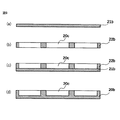
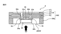
1b 集合ワイヤレス温度センサ
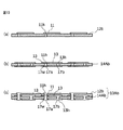
10、10A、10P 蓋
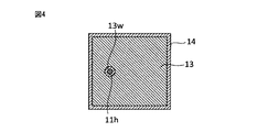
11 アンテナ電極
11h アンテナビアホール
12 上層体
12b 上層体集合基板
13 GND電極
13h GNDビアホール
13w GNDパターン開口部
14 内層体
14b 内層体集合基板
15a、15b 蓋ボンディングパッド
15m、15ma 蓋実装面
16 保護層
16b 集合保護層
17w 配線電極層開口部
17a 第一の配線電極
17b 第二の配線電極
20、20A、20B 容器本体
20AW 開口部
20b 集合容器本体
20c 本体キャビティ
21b 本体底部集合基板
22b 本体側部集合基板
30 温度検出素子
31 弾性表面波素子基板
32a,32b 櫛形電極
33 反射体
34a、34b 素子ボンディングパッド
35a ボンディングワイヤ
40 温度表示装置
50、50A、50P 容器
Tw 励起弾性表面波
Rw 反射弾性表面波
Rwp 反射弾性表面波強度
T1、T2、T3 時刻
d、d1、d2、d3 電極間距離
f1,f2,f3 高周波信号
t 伝搬時間
ST1 容器本体組み立て及び高温焼成工程
ST2 蓋組み立て及び低温焼成工程
ST3 温度検出素子実装及び全体組み立て工程
dc 裁断線
Claims (22)
- ワイヤレス温度センサの製造方法であって、
第一のセラミックグリーンシートと、第二のセラミックグリーンシートと、を用意する工程と、
前記第二のセラミックグリーンシートよりも熱伝導率が高い前記第一のセラミックグリーンシートを焼成して容器本体を形成する工程と、
前記第二のセラミックグリーンシートにアンテナ電極及びGND電極を配置し、前記アンテナ電極及び前記GND電極が配置された前記第二のセラミックグリーンシートを、前記第一のセラミックグリーンシートよりも低い焼成温度で焼成してアンテナを有する蓋を形成する工程と、
温度検出素子を、前記アンテナ電極及び前記GND電極に電気的に接続する工程と、
前記温度検出素子が前記容器本体及び前記蓋の内部に固定されるように、前記容器本体と前記蓋とを貼り合わせる工程と、
を有することを特徴とするワイヤレス温度センサの製造方法。 - 前記貼り合わせる工程は、前記温度検出素子が前記容器本体の内側に接触するように、前記容器本体と前記蓋とを貼り合わせる、請求項1に記載のワイヤレス温度センサの製造方法。
- 前記容器本体は、前記蓋と貼り合わされる側と反対側に開口部を有する、請求項1に記載のワイヤレス温度センサの製造方法。
- 前記容器本体と前記蓋とを貼り合わせる工程は、前記容器本体と前記温度検出素子との間に熱伝導体を配置するように、前記容器本体と前記蓋とを貼り合わせる、請求項1に記載のワイヤレス温度センサの製造方法。
- 前記容器本体は、ポーラス構造又はメッシュ構造を有する、請求項1に記載のワイヤレス温度センサの製造方法。
- 前記蓋を形成する工程は、
前記第二のセラミックグリーンシートの一方の面上に前記アンテナ電極となる導体パターンを配置し、
前記第二のセラミックグリーンシートの内層に前記GND電極となる導体パターンを配置し、
前記第二のセラミックグリーンシートに、前記アンテナ電極と導通する第一のビアホール及び前記GND電極と導通する第二のビアホールを形成し、
前記第二のセラミックグリーンシートの他方の面上に、前記第一のビアホールと導通する第一の電極パッド及び前記第二のビアホールと導通する第二の電極パッドを形成する、
請求項1〜5の何れか一項に記載のワイヤレス温度センサの製造方法。 - 前記蓋を形成する工程は、前記第二のセラミックグリーンシートの前記他方の面上に、前記第二の電極パッドと導通し、且つ、前記温度検出素子及び前記容器本体に熱的に接続する熱伝導層を形成する、請求項6に記載のワイヤレス温度センサの製造方法。
- 前記温度検出素子を前記熱伝導層上の前記第二のビアホールの上に固定する工程をさらに有する、請求項7に記載のワイヤレス温度センサの製造方法。
- 前記アンテナ電極を覆う保護層を前記第二のセラミックグリーンシート上に形成する工程を更に有する、請求項1〜8の何れか一項に記載のワイヤレス温度センサの製造方法。
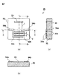
- 第一のセラミック基板から形成された容器本体と、
前記第一のセラミック基板よりも焼成温度が低い第二のセラミック基板で形成された蓋と、
アンテナと、
温度検出素子と、を備え、
前記第一のセラミック基板は、前記第二のセラミック基板よりも熱伝導率が高く、
前記アンテナは、前記蓋に一体的に形成されたアンテナ電極及びGND電極を含み、
前記温度検出素子は、前記アンテナ電極及び前記GND電極に電気的に接続され、前記容器本体と前記蓋とが貼り合わされることによって前記容器本体及び前記蓋の内部に固定されている、
ことを特徴とするワイヤレス温度センサ。 - 前記温度検出素子は、前記容器本体の内側に接触するように、前記容器本体及び前記蓋の内部に固定されている、請求項10に記載のワイヤレス温度センサ。
- 前記容器本体は、前記蓋と貼り合わされる側と反対側に開口部を有する、請求項10に記載のワイヤレス温度センサ。
- 前記容器本体と前記温度検出素子との間に配置された熱伝導体をさらに備える、請求項10に記載のワイヤレス温度センサ。
- 前記容器本体は、ポーラス構造又はメッシュ構造を有する、請求項10に記載のワイヤレス温度センサ。
- 前記第一のセラミック基板は、HTCC(High Temperature Cofired Ceramics)であり、
前記第二のセラミック基板は、LTCC(Low Temperature Cofired Ceramics)である、請求項10〜14の何れか一項に記載のワイヤレス温度センサ。 - 前記アンテナのアンテナ電極の材料は、銀(Ag)又は銅(Cu)である、請求項10〜15の何れか一項に記載のワイヤレス温度センサ。
- 前記容器本体と前記蓋とは熱的に接続され、前記温度検出素子と前記蓋とは熱的に接続されている、請求項10〜16の何れか一項に記載のワイヤレス温度センサ。
- 前記アンテナ電極は前記第二のセラミック基板の表面に形成され、前記GND電極は前記第二のセラミック基板の内層に形成される、請求項10〜17の何れか一項に記載のワイヤレス温度センサ。
- 前記第二のセラミック基板の裏面に形成された第一の配線電極及び第二の配線電極をさらに備え、
前記第一の配線電極は前記温度検出素子と前記アンテナ電極とにそれぞれ電気的に接続され、
前記第二の配線電極は前記温度検出素子と前記GND電極とにそれぞれ電気的に接続されている、請求項10〜18の何れか一項に記載のワイヤレス温度センサ。 - 前記第二の配線電極は前記温度検出素子及び前記容器本体に熱的に接続されている、請求項19に記載のワイヤレス温度センサ。
- 前記第二のセラミック基板内に形成され、前記GND電極及び前記第二の配線電極と導通するビアホールをさらに備え、
前記温度検出素子は、前記第二の配線電極上の前記ビアホールの上に固定される請求項20に記載のワイヤレス温度センサ。 - 前記アンテナ電極を覆う保護層をさらに備える、請求項10〜21の何れか一項に記載のワイヤレス温度センサ。
Priority Applications (1)
| Application Number | Priority Date | Filing Date | Title |
|---|---|---|---|
| JP2015042968A JP6516513B2 (ja) | 2014-03-06 | 2015-03-04 | ワイヤレス温度センサ及びその製造方法 |
Applications Claiming Priority (3)
| Application Number | Priority Date | Filing Date | Title |
|---|---|---|---|
| JP2014043932 | 2014-03-06 | ||
| JP2014043932 | 2014-03-06 | ||
| JP2015042968A JP6516513B2 (ja) | 2014-03-06 | 2015-03-04 | ワイヤレス温度センサ及びその製造方法 |
Publications (3)
| Publication Number | Publication Date |
|---|---|
| JP2015180871A JP2015180871A (ja) | 2015-10-15 |
| JP2015180871A5 JP2015180871A5 (ja) | 2018-02-08 |
| JP6516513B2 true JP6516513B2 (ja) | 2019-05-22 |
Family
ID=54329175
Family Applications (1)
| Application Number | Title | Priority Date | Filing Date |
|---|---|---|---|
| JP2015042968A Active JP6516513B2 (ja) | 2014-03-06 | 2015-03-04 | ワイヤレス温度センサ及びその製造方法 |
Country Status (1)
| Country | Link |
|---|---|
| JP (1) | JP6516513B2 (ja) |
Families Citing this family (2)
| Publication number | Priority date | Publication date | Assignee | Title |
|---|---|---|---|---|
| JP6852289B2 (ja) * | 2016-06-20 | 2021-03-31 | 富士電機株式会社 | ワイヤレスセンサシステム |
| KR20210005335A (ko) * | 2019-07-03 | 2021-01-14 | 주식회사 에스아이피 | 무선 데이터 송신형 센서 시스템 |
Family Cites Families (3)
| Publication number | Priority date | Publication date | Assignee | Title |
|---|---|---|---|---|
| US6796187B2 (en) * | 2000-12-08 | 2004-09-28 | The Johns Hopkins University | Wireless multi-functional sensor platform, system containing same and method for its use |
| JP2006259156A (ja) * | 2005-03-16 | 2006-09-28 | Fuji Xerox Co Ltd | 画像形成装置 |
| US8730681B2 (en) * | 2011-09-23 | 2014-05-20 | Infineon Technologies Ag | Power semiconductor module with wireless saw temperature sensor |
-
2015
- 2015-03-04 JP JP2015042968A patent/JP6516513B2/ja active Active
Also Published As
| Publication number | Publication date |
|---|---|
| JP2015180871A (ja) | 2015-10-15 |
Similar Documents
| Publication | Publication Date | Title |
|---|---|---|
| WO2015133541A1 (ja) | ワイヤレス温度センサ | |
| JP6170349B2 (ja) | 弾性波デバイス | |
| US8384486B2 (en) | Piezoelectric oscillator and transmitter | |
| US8730681B2 (en) | Power semiconductor module with wireless saw temperature sensor | |
| JP6541375B2 (ja) | ワイヤレス温度センサ及びその製造方法 | |
| JP2018207144A (ja) | 弾性波デバイス | |
| JP2017156123A (ja) | ワイヤレス温度センサ | |
| JP2006047085A (ja) | 赤外線センサ装置およびその製造方法 | |
| JP2010177732A (ja) | 恒温型圧電発振器 | |
| JP6516513B2 (ja) | ワイヤレス温度センサ及びその製造方法 | |
| JP2019161408A (ja) | 弾性波デバイス、モジュールおよびマルチプレクサ | |
| KR101616639B1 (ko) | 표면 탄성파 소자 및 그 실장 장치, 이를 이용한 측정 센서 | |
| US10367510B2 (en) | Crystal oscillator and method for manufacturing crystal oscillator | |
| JP7119119B2 (ja) | 配線基板、電子部品搭載用パッケージおよび電子装置 | |
| JP7340344B2 (ja) | 弾性波デバイス、フィルタおよびマルチプレクサ | |
| JP7426196B2 (ja) | 弾性波デバイスおよびその製造方法、フィルタ及びマルチプレクサ | |
| US20180219526A1 (en) | Component with improved heat dissipation | |
| JP4175085B2 (ja) | ワイヤレス温度計測モジュール | |
| JP2017133849A (ja) | ワイヤレス温度センサ | |
| JP6208543B2 (ja) | パッケージおよび電子装置 | |
| JP6279857B2 (ja) | 電子装置、多数個取り枠体および多数個取り電子装置 | |
| JP7235378B2 (ja) | 弾性表面波センサおよびそれを用いた計測システム | |
| JP5705491B2 (ja) | 電子部品搭載用パッケージおよびそれを用いた電子装置 | |
| JP4511207B2 (ja) | 圧力センサモジュール | |
| JP2006337135A (ja) | 圧電センサモジュール及び圧電センサシステム |
Legal Events
| Date | Code | Title | Description |
|---|---|---|---|
| A521 | Request for written amendment filed |
Free format text: JAPANESE INTERMEDIATE CODE: A523 Effective date: 20171219 |
|
| A621 | Written request for application examination |
Free format text: JAPANESE INTERMEDIATE CODE: A621 Effective date: 20171219 |
|
| A977 | Report on retrieval |
Free format text: JAPANESE INTERMEDIATE CODE: A971007 Effective date: 20181024 |
|
| A131 | Notification of reasons for refusal |
Free format text: JAPANESE INTERMEDIATE CODE: A131 Effective date: 20181106 |
|
| A601 | Written request for extension of time |
Free format text: JAPANESE INTERMEDIATE CODE: A601 Effective date: 20181226 |
|
| A521 | Request for written amendment filed |
Free format text: JAPANESE INTERMEDIATE CODE: A523 Effective date: 20190304 |
|
| TRDD | Decision of grant or rejection written | ||
| A01 | Written decision to grant a patent or to grant a registration (utility model) |
Free format text: JAPANESE INTERMEDIATE CODE: A01 Effective date: 20190319 |
|
| A61 | First payment of annual fees (during grant procedure) |
Free format text: JAPANESE INTERMEDIATE CODE: A61 Effective date: 20190416 |
|
| R150 | Certificate of patent or registration of utility model |
Ref document number: 6516513 Country of ref document: JP Free format text: JAPANESE INTERMEDIATE CODE: R150 |
|
| R250 | Receipt of annual fees |
Free format text: JAPANESE INTERMEDIATE CODE: R250 |