JP6469554B2 - 半導体装置 - Google Patents
半導体装置 Download PDFInfo
- Publication number
- JP6469554B2 JP6469554B2 JP2015179683A JP2015179683A JP6469554B2 JP 6469554 B2 JP6469554 B2 JP 6469554B2 JP 2015179683 A JP2015179683 A JP 2015179683A JP 2015179683 A JP2015179683 A JP 2015179683A JP 6469554 B2 JP6469554 B2 JP 6469554B2
- Authority
- JP
- Japan
- Prior art keywords
- word line
- voltage
- semiconductor device
- pmos transistor
- driver
- Prior art date
- Legal status (The legal status is an assumption and is not a legal conclusion. Google has not performed a legal analysis and makes no representation as to the accuracy of the status listed.)
- Active
Links
Images


Classifications
-
- G—PHYSICS
- G11—INFORMATION STORAGE
- G11C—STATIC STORES
- G11C11/00—Digital stores characterised by the use of particular electric or magnetic storage elements; Storage elements therefor
- G11C11/21—Digital stores characterised by the use of particular electric or magnetic storage elements; Storage elements therefor using electric elements
- G11C11/34—Digital stores characterised by the use of particular electric or magnetic storage elements; Storage elements therefor using electric elements using semiconductor devices
- G11C11/40—Digital stores characterised by the use of particular electric or magnetic storage elements; Storage elements therefor using electric elements using semiconductor devices using transistors
- G11C11/41—Digital stores characterised by the use of particular electric or magnetic storage elements; Storage elements therefor using electric elements using semiconductor devices using transistors forming static cells with positive feedback, i.e. cells not needing refreshing or charge regeneration, e.g. bistable multivibrator or Schmitt trigger
- G11C11/413—Auxiliary circuits, e.g. for addressing, decoding, driving, writing, sensing, timing or power reduction
- G11C11/417—Auxiliary circuits, e.g. for addressing, decoding, driving, writing, sensing, timing or power reduction for memory cells of the field-effect type
- G11C11/419—Read-write [R-W] circuits
-
- G—PHYSICS
- G11—INFORMATION STORAGE
- G11C—STATIC STORES
- G11C8/00—Arrangements for selecting an address in a digital store
- G11C8/08—Word line control circuits, e.g. drivers, boosters, pull-up circuits, pull-down circuits, precharging circuits, for word lines
-
- G—PHYSICS
- G11—INFORMATION STORAGE
- G11C—STATIC STORES
- G11C11/00—Digital stores characterised by the use of particular electric or magnetic storage elements; Storage elements therefor
- G11C11/21—Digital stores characterised by the use of particular electric or magnetic storage elements; Storage elements therefor using electric elements
- G11C11/34—Digital stores characterised by the use of particular electric or magnetic storage elements; Storage elements therefor using electric elements using semiconductor devices
- G11C11/40—Digital stores characterised by the use of particular electric or magnetic storage elements; Storage elements therefor using electric elements using semiconductor devices using transistors
- G11C11/41—Digital stores characterised by the use of particular electric or magnetic storage elements; Storage elements therefor using electric elements using semiconductor devices using transistors forming static cells with positive feedback, i.e. cells not needing refreshing or charge regeneration, e.g. bistable multivibrator or Schmitt trigger
- G11C11/413—Auxiliary circuits, e.g. for addressing, decoding, driving, writing, sensing, timing or power reduction
- G11C11/417—Auxiliary circuits, e.g. for addressing, decoding, driving, writing, sensing, timing or power reduction for memory cells of the field-effect type
- G11C11/418—Address circuits
-
- G—PHYSICS
- G11—INFORMATION STORAGE
- G11C—STATIC STORES
- G11C7/00—Arrangements for writing information into, or reading information out from, a digital store
- G11C7/10—Input/output [I/O] data interface arrangements, e.g. I/O data control circuits, I/O data buffers
- G11C7/1075—Input/output [I/O] data interface arrangements, e.g. I/O data control circuits, I/O data buffers for multiport memories each having random access ports and serial ports, e.g. video RAM
-
- H—ELECTRICITY
- H10—SEMICONDUCTOR DEVICES; ELECTRIC SOLID-STATE DEVICES NOT OTHERWISE PROVIDED FOR
- H10B—ELECTRONIC MEMORY DEVICES
- H10B10/00—Static random access memory [SRAM] devices
- H10B10/12—Static random access memory [SRAM] devices comprising a MOSFET load element
-
- H—ELECTRICITY
- H10—SEMICONDUCTOR DEVICES; ELECTRIC SOLID-STATE DEVICES NOT OTHERWISE PROVIDED FOR
- H10B—ELECTRONIC MEMORY DEVICES
- H10B10/00—Static random access memory [SRAM] devices
- H10B10/18—Peripheral circuit regions
-
- H—ELECTRICITY
- H01—ELECTRIC ELEMENTS
- H01L—SEMICONDUCTOR DEVICES NOT COVERED BY CLASS H10
- H01L27/00—Devices consisting of a plurality of semiconductor or other solid-state components formed in or on a common substrate
- H01L27/02—Devices consisting of a plurality of semiconductor or other solid-state components formed in or on a common substrate including semiconductor components specially adapted for rectifying, oscillating, amplifying or switching and having at least one potential-jump barrier or surface barrier; including integrated passive circuit elements with at least one potential-jump barrier or surface barrier
- H01L27/0203—Particular design considerations for integrated circuits
- H01L27/0207—Geometrical layout of the components, e.g. computer aided design; custom LSI, semi-custom LSI, standard cell technique
Description
[第1の実施形態]
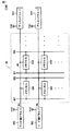
図1は、第1の実施形態の半導体装置の構成を表わす図である。
ワード線WLは、メモリアレイ98の各行に対応して設けられる。ワード線WLは、対応する行のメモリセル500と接続する。
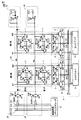
図2は、第2の実施形態の半導体装置の構成を表わす図である。
PMOSトランジスタP3,P4,P4,P20がオンとなり、第0列のビット線対BT,BBが電圧Vddでプリチャージされる。
PMOSトランジスタP3,P4,P4,P20がオフとなり、第0列のビット線対BT,BBのプリチャージが終了する。PMOSトランジスタP5,P6とNMOSトランジスタN5,N6がオンとなり、第0列のビット線対BT,BBがライトドライバ5およびセンスアンプ6と接続される。
PMOSトランジスタP3,P4,P4,P20がオンとなり、第1列のビット線対BT,BBが電圧Vddでプリチャージされる。
PMOSトランジスタP3,P4,P4,P20がオフとなり、第1列のビット線対BT,BBのプリチャージが終了する。PMOSトランジスタP5,P6とNMOSトランジスタN5,N6がオンとなり、第1列のビット線対BT,BBがライトドライバ5およびセンスアンプ6と接続される。
PMOSトランジスタP8は、ワード線WLの末端Yと、電源Vddとの間に設けられる。インバータIV3の入力は、ワード線WLの末端Yに接続され、インバータIV3の出力は、PMOSトランジスタP8のゲートに接続される。
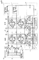
図4は、第3の実施形態の半導体装置の構成を表わす図である。
アシスト制御回路12は、2段のインバータIV4,IV5を備える。
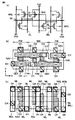
図6は、第4の実施形態の半導体装置の構成を表わす図である。
アシストドライバ13は、NAND回路NAN3と、PMOSトランジスタP8と、遅延回路DLとを備える。遅延回路DLは、3段のインバータIV6,IV7,IV8を含む。
上述の実施形態のメモリセル1は、縦長型メモリセルである。本実施の形態の半導体装置は、メモリセルとして、横長型メモリセルを含む。
Claims (11)
- 行列状に配置された複数のメモリセルを含むメモリアレイと、
前記メモリアレイの各行に対応して設けられたワード線と、
前記ワード線の一端に接続されて、対応する行が選択されたときに、前記ワード線の一端を第1の電源に接続することによってワード線を活性化するワード線ドライバと、
前記ワード線の他端に接続されて、前記ワード線の他端の電圧に応じて、前記ワード線の他端を前記第1の電源に接続するアシストドライバと、
を備え、
前記アシストドライバは、
前記第1の電源と前記ワード線の他端との間に設けられたPMOSトランジスタと、
前記ワード線の他端に接続された遅延回路と、
一方の入力が前記ワード線の他端に接続され、他方の入力が前記遅延回路の出力を受け、出力が前記PMOSトランジスタのゲートに接続されたNAND回路と、
を含む、半導体装置。 - 前記遅延回路は、奇数個の直列接続されたインバータからなる、請求項1記載の半導体装置。
- 前記ワード線ドライバは、出力が、前記ワード線の一端に接続されるインバータを含む、請求項1記載の半導体装置。
- 前記メモリセルは、SRAMセルである、請求項1記載の半導体装置。
- 前記メモリセルは、横長型セルである、請求項4記載の半導体装置。
- 前記メモリアレイの各列に対応して設けられたビット線対と、
隣接する複数の列のビット線対と接続され、前記メモリセルへのデータの書込み時に、前記隣接する複数の列のうちの選択された列のビット線対へ書込みデータに応じた電圧を出力する、請求項1記載の半導体装置。 - 前記メモリアレイの各列に対応して設けられたビット線対と、
隣接する複数の列のビット線対と接続され、前記メモリセルからのデータの読出し時に、前記隣接する複数の列のうちの選択された列のビット線対の電圧を増幅するセンスアンプとを備える、請求項1記載の半導体装置。 - 行列状に配置された複数のメモリセルを含むメモリアレイと、
前記メモリアレイの各行に対応して設けられたワード線と、
前記ワード線の一端に接続されて、対応する行が選択されたときに、前記ワード線の一端を第1の電源に接続するワード線ドライバと、
前記第1の電源と前記ワード線の他端との間に設けられたPMOSトランジスタと、
前記ワード線の他端に接続された遅延回路と、
一方の入力が前記ワード線の他端に接続され、他方の入力が前記遅延回路の出力を受け、出力が前記PMOSトランジスタのゲートに接続されたNAND回路と、
を備え、
前記PMOSトランジスタは、前記ワード線の立ち上がり時に、前記ワード線の他端の電圧が所定値まで増加するとオンとなり、前記ワード線の立下り時に、制御信号によってオフとなる、半導体装置。 - 前記遅延回路は、奇数個の直列接続されたインバータからなる、請求項8記載の半導体装置。
- 行列状に配置された複数のメモリセルを含むメモリアレイと、
前記メモリアレイの各行に対応して設けられたワード線と、
前記ワード線の一端に接続されて、対応する行が選択されたときに、前記ワード線の一端を第1の電源に接続するワード線ドライバと、
前記第1の電源と前記ワード線の他端との間に設けられたPMOSトランジスタと、
前記ワード線の他端に接続された遅延回路と、
一方の入力が前記ワード線の他端に接続され、他方の入力が前記遅延回路の出力を受け、出力が前記PMOSトランジスタのゲートに接続されたNAND回路と、
を備え、
前記PMOSトランジスタは、前記ワード線の立ち上がり時に、前記ワード線の他端の電圧が所定値まで立ち上がった時から所定時間だけロウレベルとなるワンショットパルスによって、オンとなる、半導体装置。 - 前記遅延回路は、奇数個の直列接続されたインバータからなる、請求項10記載の半導体装置。
Priority Applications (5)
| Application Number | Priority Date | Filing Date | Title |
|---|---|---|---|
| JP2015179683A JP6469554B2 (ja) | 2015-09-11 | 2015-09-11 | 半導体装置 |
| US15/212,162 US9721647B2 (en) | 2015-09-11 | 2016-07-15 | Semiconductor device |
| CN201610704791.5A CN106531206B (zh) | 2015-09-11 | 2016-08-22 | 半导体器件 |
| US15/627,535 US10255970B2 (en) | 2015-09-11 | 2017-06-20 | Semiconductor device |
| US16/145,342 US10354722B2 (en) | 2015-09-11 | 2018-09-28 | Semiconductor device |
Applications Claiming Priority (1)
| Application Number | Priority Date | Filing Date | Title |
|---|---|---|---|
| JP2015179683A JP6469554B2 (ja) | 2015-09-11 | 2015-09-11 | 半導体装置 |
Publications (3)
| Publication Number | Publication Date |
|---|---|
| JP2017054570A JP2017054570A (ja) | 2017-03-16 |
| JP2017054570A5 JP2017054570A5 (ja) | 2018-06-28 |
| JP6469554B2 true JP6469554B2 (ja) | 2019-02-13 |
Family
ID=58238935
Family Applications (1)
| Application Number | Title | Priority Date | Filing Date |
|---|---|---|---|
| JP2015179683A Active JP6469554B2 (ja) | 2015-09-11 | 2015-09-11 | 半導体装置 |
Country Status (3)
| Country | Link |
|---|---|
| US (3) | US9721647B2 (ja) |
| JP (1) | JP6469554B2 (ja) |
| CN (1) | CN106531206B (ja) |
Families Citing this family (8)
| Publication number | Priority date | Publication date | Assignee | Title |
|---|---|---|---|---|
| JP6469554B2 (ja) * | 2015-09-11 | 2019-02-13 | ルネサスエレクトロニクス株式会社 | 半導体装置 |
| US9786363B1 (en) * | 2016-11-01 | 2017-10-10 | Taiwan Semiconductor Manufacturing Co., Ltd. | Word-line enable pulse generator, SRAM and method for adjusting word-line enable time of SRAM |
| US10943645B2 (en) * | 2018-07-31 | 2021-03-09 | Taiwan Semiconductor Manufacturing Company, Ltd | Memory device with a booster word line |
| JP7270451B2 (ja) | 2019-04-26 | 2023-05-10 | ルネサスエレクトロニクス株式会社 | 半導体装置および半導体装置の駆動方法 |
| JP2021108307A (ja) * | 2019-12-27 | 2021-07-29 | キオクシア株式会社 | 半導体記憶装置 |
| US11170830B2 (en) * | 2020-02-11 | 2021-11-09 | Taiwan Semiconductor Manufacturing Company Limited | Word line driver for low voltage operation |
| KR20220058284A (ko) | 2020-10-30 | 2022-05-09 | 삼성전자주식회사 | 워드 라인 보조 셀을 갖는 셀 어레이를 포함하는 집적 회로 |
| US11521670B2 (en) * | 2020-11-12 | 2022-12-06 | Micron Technology, Inc. | Word lines coupled to pull-down transistors, and related devices, systems, and methods |
Family Cites Families (15)
| Publication number | Priority date | Publication date | Assignee | Title |
|---|---|---|---|---|
| JPS55150189A (en) | 1979-05-10 | 1980-11-21 | Nec Corp | Memory circuit |
| JPS60226095A (ja) * | 1984-04-25 | 1985-11-11 | Hitachi Micro Comput Eng Ltd | 半導体記憶装置 |
| JPS63276793A (ja) * | 1987-05-07 | 1988-11-15 | Nec Ic Microcomput Syst Ltd | ワ−ド線駆動回路 |
| JPH06203579A (ja) * | 1993-01-08 | 1994-07-22 | Fujitsu Ltd | 出力回路及び記憶装置 |
| JP3908493B2 (ja) * | 2001-08-30 | 2007-04-25 | 株式会社東芝 | 電子回路及び半導体記憶装置 |
| JP4439167B2 (ja) * | 2002-08-30 | 2010-03-24 | 株式会社ルネサステクノロジ | 半導体記憶装置 |
| US7064981B2 (en) * | 2004-08-04 | 2006-06-20 | Micron Technology, Inc. | NAND string wordline delay reduction |
| JP4912016B2 (ja) * | 2005-05-23 | 2012-04-04 | ルネサスエレクトロニクス株式会社 | 半導体記憶装置 |
| JP4631743B2 (ja) | 2006-02-27 | 2011-02-16 | ソニー株式会社 | 半導体装置 |
| US7379354B2 (en) * | 2006-05-16 | 2008-05-27 | Texas Instruments Incorporated | Methods and apparatus to provide voltage control for SRAM write assist circuits |
| US7733686B2 (en) * | 2006-12-30 | 2010-06-08 | Texas Instruments Incorporated | Pulse width control for read and write assist for SRAM circuits |
| US8014226B2 (en) * | 2009-12-22 | 2011-09-06 | Arm Limited | Integrated circuit memory with word line driving helper circuits |
| JP2014067942A (ja) * | 2012-09-27 | 2014-04-17 | Toshiba Corp | 不揮発性半導体記憶装置 |
| JP2014099225A (ja) | 2012-11-14 | 2014-05-29 | Renesas Electronics Corp | 半導体装置 |
| JP6469554B2 (ja) * | 2015-09-11 | 2019-02-13 | ルネサスエレクトロニクス株式会社 | 半導体装置 |
-
2015
- 2015-09-11 JP JP2015179683A patent/JP6469554B2/ja active Active
-
2016
- 2016-07-15 US US15/212,162 patent/US9721647B2/en active Active
- 2016-08-22 CN CN201610704791.5A patent/CN106531206B/zh active Active
-
2017
- 2017-06-20 US US15/627,535 patent/US10255970B2/en active Active
-
2018
- 2018-09-28 US US16/145,342 patent/US10354722B2/en active Active
Also Published As
| Publication number | Publication date |
|---|---|
| CN106531206B (zh) | 2022-05-27 |
| US10354722B2 (en) | 2019-07-16 |
| JP2017054570A (ja) | 2017-03-16 |
| US20190035456A1 (en) | 2019-01-31 |
| US10255970B2 (en) | 2019-04-09 |
| US20170287553A1 (en) | 2017-10-05 |
| CN106531206A (zh) | 2017-03-22 |
| US20170076785A1 (en) | 2017-03-16 |
| US9721647B2 (en) | 2017-08-01 |
Similar Documents
| Publication | Publication Date | Title |
|---|---|---|
| JP6469554B2 (ja) | 半導体装置 | |
| JP4553185B2 (ja) | 半導体集積回路装置 | |
| US7697320B2 (en) | Semiconductor memory device | |
| TWI415126B (zh) | 半導體記憶體 | |
| JP2009070480A (ja) | 半導体記憶装置 | |
| JP4598420B2 (ja) | 半導体記憶装置、及びタイミング制御方法 | |
| US20130258794A1 (en) | Memory device having control circuitry for sense amplifier reaction time tracking | |
| US8144523B2 (en) | Semiconductor storage device | |
| JP2012128895A (ja) | 半導体記憶装置 | |
| JP2008219232A5 (ja) | ||
| JP4245147B2 (ja) | 階層ワード線方式の半導体記憶装置と、それに使用されるサブワードドライバ回路 | |
| US7489581B2 (en) | Semiconductor memory | |
| JP5586038B2 (ja) | 半導体集積回路装置 | |
| JP5456571B2 (ja) | 半導体集積回路装置 | |
| JP5867275B2 (ja) | 半導体記憶装置およびそのデータ書き込み方法 | |
| US8125820B2 (en) | Semiconductor memory device | |
| TWI751845B (zh) | 記憶體裝置以及用於操作記憶體裝置的方法 | |
| US20230282274A1 (en) | Memory device and method of operating the same | |
| JP7270451B2 (ja) | 半導体装置および半導体装置の駆動方法 | |
| JP2015111489A (ja) | 半導体集積回路装置 | |
| JP2013041663A (ja) | 半導体集積回路装置 | |
| JP2014139860A (ja) | 半導体集積回路装置 | |
| JP2006085785A (ja) | 半導体集積回路装置 |
Legal Events
| Date | Code | Title | Description |
|---|---|---|---|
| A521 | Request for written amendment filed |
Free format text: JAPANESE INTERMEDIATE CODE: A523 Effective date: 20180514 |
|
| A621 | Written request for application examination |
Free format text: JAPANESE INTERMEDIATE CODE: A621 Effective date: 20180514 |
|
| A977 | Report on retrieval |
Free format text: JAPANESE INTERMEDIATE CODE: A971007 Effective date: 20180919 |
|
| A131 | Notification of reasons for refusal |
Free format text: JAPANESE INTERMEDIATE CODE: A131 Effective date: 20181002 |
|
| A521 | Request for written amendment filed |
Free format text: JAPANESE INTERMEDIATE CODE: A523 Effective date: 20181203 |
|
| TRDD | Decision of grant or rejection written | ||
| A01 | Written decision to grant a patent or to grant a registration (utility model) |
Free format text: JAPANESE INTERMEDIATE CODE: A01 Effective date: 20181218 |
|
| A61 | First payment of annual fees (during grant procedure) |
Free format text: JAPANESE INTERMEDIATE CODE: A61 Effective date: 20190116 |
|
| R150 | Certificate of patent or registration of utility model |
Ref document number: 6469554 Country of ref document: JP Free format text: JAPANESE INTERMEDIATE CODE: R150 |