JP6469554B2 - Semiconductor device - Google Patents
Semiconductor device Download PDFInfo
- Publication number
- JP6469554B2 JP6469554B2 JP2015179683A JP2015179683A JP6469554B2 JP 6469554 B2 JP6469554 B2 JP 6469554B2 JP 2015179683 A JP2015179683 A JP 2015179683A JP 2015179683 A JP2015179683 A JP 2015179683A JP 6469554 B2 JP6469554 B2 JP 6469554B2
- Authority
- JP
- Japan
- Prior art keywords
- word line
- voltage
- semiconductor device
- pmos transistor
- driver
- Prior art date
- Legal status (The legal status is an assumption and is not a legal conclusion. Google has not performed a legal analysis and makes no representation as to the accuracy of the status listed.)
- Active
Links
Images


Classifications
-
- G—PHYSICS
- G11—INFORMATION STORAGE
- G11C—STATIC STORES
- G11C11/00—Digital stores characterised by the use of particular electric or magnetic storage elements; Storage elements therefor
- G11C11/21—Digital stores characterised by the use of particular electric or magnetic storage elements; Storage elements therefor using electric elements
- G11C11/34—Digital stores characterised by the use of particular electric or magnetic storage elements; Storage elements therefor using electric elements using semiconductor devices
- G11C11/40—Digital stores characterised by the use of particular electric or magnetic storage elements; Storage elements therefor using electric elements using semiconductor devices using transistors
- G11C11/41—Digital stores characterised by the use of particular electric or magnetic storage elements; Storage elements therefor using electric elements using semiconductor devices using transistors forming static cells with positive feedback, i.e. cells not needing refreshing or charge regeneration, e.g. bistable multivibrator or Schmitt trigger
- G11C11/413—Auxiliary circuits, e.g. for addressing, decoding, driving, writing, sensing, timing or power reduction
- G11C11/417—Auxiliary circuits, e.g. for addressing, decoding, driving, writing, sensing, timing or power reduction for memory cells of the field-effect type
- G11C11/419—Read-write [R-W] circuits
-
- G—PHYSICS
- G11—INFORMATION STORAGE
- G11C—STATIC STORES
- G11C8/00—Arrangements for selecting an address in a digital store
- G11C8/08—Word line control circuits, e.g. drivers, boosters, pull-up circuits, pull-down circuits, precharging circuits, for word lines
-
- G—PHYSICS
- G11—INFORMATION STORAGE
- G11C—STATIC STORES
- G11C11/00—Digital stores characterised by the use of particular electric or magnetic storage elements; Storage elements therefor
- G11C11/21—Digital stores characterised by the use of particular electric or magnetic storage elements; Storage elements therefor using electric elements
- G11C11/34—Digital stores characterised by the use of particular electric or magnetic storage elements; Storage elements therefor using electric elements using semiconductor devices
- G11C11/40—Digital stores characterised by the use of particular electric or magnetic storage elements; Storage elements therefor using electric elements using semiconductor devices using transistors
- G11C11/41—Digital stores characterised by the use of particular electric or magnetic storage elements; Storage elements therefor using electric elements using semiconductor devices using transistors forming static cells with positive feedback, i.e. cells not needing refreshing or charge regeneration, e.g. bistable multivibrator or Schmitt trigger
- G11C11/413—Auxiliary circuits, e.g. for addressing, decoding, driving, writing, sensing, timing or power reduction
- G11C11/417—Auxiliary circuits, e.g. for addressing, decoding, driving, writing, sensing, timing or power reduction for memory cells of the field-effect type
- G11C11/418—Address circuits
-
- G—PHYSICS
- G11—INFORMATION STORAGE
- G11C—STATIC STORES
- G11C7/00—Arrangements for writing information into, or reading information out from, a digital store
- G11C7/10—Input/output [I/O] data interface arrangements, e.g. I/O data control circuits, I/O data buffers
- G11C7/1075—Input/output [I/O] data interface arrangements, e.g. I/O data control circuits, I/O data buffers for multiport memories each having random access ports and serial ports, e.g. video RAM
-
- H—ELECTRICITY
- H10—SEMICONDUCTOR DEVICES; ELECTRIC SOLID-STATE DEVICES NOT OTHERWISE PROVIDED FOR
- H10B—ELECTRONIC MEMORY DEVICES
- H10B10/00—Static random access memory [SRAM] devices
- H10B10/12—Static random access memory [SRAM] devices comprising a MOSFET load element
-
- H—ELECTRICITY
- H10—SEMICONDUCTOR DEVICES; ELECTRIC SOLID-STATE DEVICES NOT OTHERWISE PROVIDED FOR
- H10B—ELECTRONIC MEMORY DEVICES
- H10B10/00—Static random access memory [SRAM] devices
- H10B10/18—Peripheral circuit regions
-
- H—ELECTRICITY
- H01—ELECTRIC ELEMENTS
- H01L—SEMICONDUCTOR DEVICES NOT COVERED BY CLASS H10
- H01L27/00—Devices consisting of a plurality of semiconductor or other solid-state components formed in or on a common substrate
- H01L27/02—Devices consisting of a plurality of semiconductor or other solid-state components formed in or on a common substrate including semiconductor components specially adapted for rectifying, oscillating, amplifying or switching and having at least one potential-jump barrier or surface barrier; including integrated passive circuit elements with at least one potential-jump barrier or surface barrier
- H01L27/0203—Particular design considerations for integrated circuits
- H01L27/0207—Geometrical layout of the components, e.g. computer aided design; custom LSI, semi-custom LSI, standard cell technique
Description
本発明は、半導体装置に関し、たとえば、ワード線の活性化によってデータの書込みおよび読出しが実行されるメモリセルを有する半導体装置に関する。 The present invention relates to a semiconductor device, for example, a semiconductor device having a memory cell in which data is written and read by activation of a word line.
従来から、行列状に配置された複数のメモリセルを含むメモリアレイと、メモリアレイの各行に設けられたワード線と、メモリセルからのデータの読出し時および書込み時におおいて、選択された行のワード線を活性化するワード線ドライバを備えた半導体装置が知られている(たとえば、特許文献1を参照)。 Conventionally, a memory array including a plurality of memory cells arranged in a matrix, a word line provided in each row of the memory array, and a selected row at the time of reading and writing data from the memory cell A semiconductor device including a word line driver that activates a word line is known (see, for example, Patent Document 1).
しかしながら、近年、トランジスタの駆動力向上および配線の微細化が進み、配線の抵抗成分の影響が顕在化している。 However, in recent years, the driving force of transistors and the miniaturization of wiring have progressed, and the influence of resistance components of wiring has become obvious.
メモリアレイを含む半導体装置においては、ワード線の抵抗成分の影響によって、ワード線の活性化時において、ワード線ドライバに近い箇所の電圧の立ち上がり速度に比べて、ワード線ドライバから遠い箇所の電圧の立ち上がり速度が遅いという問題が生じている。その結果、ワード線ドライバから遠い箇所のメモリセルでは、ワード線ドライバから近い箇所のメモリセルに比べて、セル電流が流れ始めるのが遅くなり、メモリセルへのデータの書込みおよびメモリセルからのデータの読出しが遅れる。 In a semiconductor device including a memory array, due to the influence of the resistance component of the word line, when the word line is activated, the voltage at a location far from the word line driver is higher than the rising speed of the voltage near the word line driver. There is a problem that the rising speed is slow. As a result, in the memory cell far from the word line driver, the cell current starts to flow more slowly than in the memory cell near the word line driver, so that data is written to and read from the memory cell. Is delayed.
その他の課題と新規な特徴は、本明細書の記述および添付図面から明らかであろう。 Other problems and novel features will be apparent from the description of this specification and the accompanying drawings.
一実施形態の半導体装置は、ワード線ドライバが接続されていない側のワード線の他端に接続されて、ワード線の他端の電圧に応じて、ワード線の他端を第1の電源に接続するアシストドライバを備える。 In one embodiment, the semiconductor device is connected to the other end of the word line to which the word line driver is not connected, and the other end of the word line is used as a first power supply according to the voltage at the other end of the word line. An assist driver for connection is provided.
一実施形態の半導体装置によれば、ワード線の活性化時において、ワード線ドライバに近い箇所の電圧の立ち上がり速度に比べて、ワード線ドライバから遠い箇所の電圧の立ち上がり速度が遅くなるのを回避できる。 According to the semiconductor device of one embodiment, when the word line is activated, it is avoided that the rising speed of the voltage at a location far from the word line driver is slow compared to the rising speed of the voltage at a location near the word line driver. it can.
以下、本発明の実施形態について図面を用いて説明する。
[第1の実施形態]
図1は、第1の実施形態の半導体装置の構成を表わす図である。
Hereinafter, embodiments of the present invention will be described with reference to the drawings.
[First Embodiment]
FIG. 1 is a diagram illustrating the configuration of the semiconductor device according to the first embodiment.
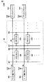
図1を参照して、この半導体装置1000は、メモリアレイ98と、複数個のワード線WLと、複数個のビット線対BT,BBと、複数個のワード線ドライバ502と、第1の電源Vddと、複数個のアシストドライバ504とを備える。
Referring to FIG. 1, a
メモリアレイ98は、行列状に配置された複数個のメモリセル500を含む。
ワード線WLは、メモリアレイ98の各行に対応して設けられる。ワード線WLは、対応する行のメモリセル500と接続する。
Word line WL is provided corresponding to each row of
ビット線対BT,BBは、メモリアレイ98の各列に対応して設けられる。ビット線対BT,BBは、対応する列のメモリセル500と接続する。
Bit line pair BT, BB is provided corresponding to each column of
ワード線ドライバ502は、ワード線WLの一端に接続されて、対応する行が選択されたときに、ワード線WLの一端を第1の電源Vddに接続する。
The
アシストドライバ504は、ワード線WLの他端に接続されて、ワード線WLの他端の電圧に応じて、ワード線WLの他端を第1の電源Vddに接続する。
The
以上のように、本実施の形態によれば、アシストドライバ504によって、ワード線WLの他端の電圧が立ち上げられるので、ワード線WLの活性化時において、ワード線ドライバ502に近い箇所の電圧の立ち上がり速度に比べて、ワード線ドライバ502から遠い箇所の電圧の立ち上がり速度が遅くなるのを回避できる。
As described above, according to the present embodiment, the voltage at the other end of the word line WL is raised by the
[第2の実施形態]
図2は、第2の実施形態の半導体装置の構成を表わす図である。
[Second Embodiment]
FIG. 2 is a diagram illustrating the configuration of the semiconductor device according to the second embodiment.
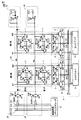
半導体装置100は、メモリアレイ62と、複数個のワード線WLと、複数個のビット線対BT,BBと、複数個のワード線ドライバ22と、複数個のアシストドライバ10と、複数個のカラムセレクタ4と、複数個のプリチャージ回路3と、制御回路・アドレスデコーダ21と、複数個のライトドライバ5と、複数個のセンスアンプ6とを備える。
The
メモリアレイ62は、行列状に配置された複数個のメモリセル1を含む。図2では、複数個のメモリセル1を代表して2行2列のメモリセルを示す。メモリセル1は、SRAM(Static Random Access Memory)セルである。
メモリセル1は、負荷トランジスタであるPMOS(Metal-Oxide-Semiconductor)トランジスタP1,P2と、ドライバトランジスタであるNMOトランジスタN1,N2と、アクセストランジスタであるNMOSトランジスタN20,N21とを含む。
The
負荷トランジスタP1,P2のソースはともに内部電源電圧Vddに接続され、それらのドレインはそれぞれ記憶ノードA,Bに接続され、それらのゲートはそれぞれ記憶ノードB,Aに接続される。 The sources of load transistors P1 and P2 are both connected to internal power supply voltage Vdd, their drains are connected to storage nodes A and B, respectively, and their gates are connected to storage nodes B and A, respectively.
ドライバトランジスタN1,N2のソースはともに接地電源(グランド)に接続され、それらのドレインはそれぞれ記憶ノードA,Bに接続され、それらのゲートはそれぞれ記憶ノードB,Aに接続される。 The sources of driver transistors N1 and N2 are both connected to a ground power supply (ground), their drains are connected to storage nodes A and B, respectively, and their gates are connected to storage nodes B and A, respectively.
アクセストランジスタN20,N21のソースはそれぞれ記憶ノードA,Bに接続され、それらのドレインはそれぞれ対応のビット線BT,BBに接続され、それらのゲートはともに対応のワード線WLに接続される。 The sources of access transistors N20 and N21 are connected to storage nodes A and B, respectively, their drains are connected to corresponding bit lines BT and BB, respectively, and their gates are connected to a corresponding word line WL.
PMOSトランジスタP1およびNMOSトランジスタN1は、インバータを構成し、記憶ノードBに書込まれたデータの反転信号を記憶ノードAに出力する。PMOSトランジスタP2およびNMOSトランジスタN2は、インバータを構成し、記憶ノードAに書込まれたデータの反転信号を記憶ノードBに出力する。したがって、PMOSトランジスタP1,P2およびNMOSトランジスタN1,N2は、記憶ノードA,Bに書込まれたデータを保持するラッチ回路を構成する。 PMOS transistor P1 and NMOS transistor N1 form an inverter, and output an inverted signal of data written to storage node B to storage node A. PMOS transistor P2 and NMOS transistor N2 form an inverter, and output an inverted signal of data written in storage node A to storage node B. Therefore, PMOS transistors P1 and P2 and NMOS transistors N1 and N2 form a latch circuit that holds data written to storage nodes A and B.
ワード線WLは、メモリアレイ62の各行に対応して設けられる。ワード線WLは、対応する行のメモリセル500と接続する。
The word line WL is provided corresponding to each row of the
ビット線対BT,BBは、メモリアレイ62の各列に対応して設けられる。ビット線対BT,BBは、対応する列のメモリセル500と接続する。
Bit line pair BT, BB is provided corresponding to each column of
制御回路・アドレスデコーダ21は、アドレス指定されたワード線WLを選択状態に駆動するために、行アドレス信号に従って行選択信号を生成する行デコーダと、列アドレス信号に従って選択列に対応するビット線対を選択する列デコーダとを含む。
The control circuit /
具体的には、行デコーダは、読出動作時または書込動作時に、行アドレス信号をデコードして行選択信号を生成する。たとえば、行デコーダは、図2に示す第0行を選択するときには、セレクト信号XU0およびXL0をハイレベルに活性化し、図2に示す第1行を選択するときには、セレクト信号XU1およびXL1をハイレベルに活性化する。 Specifically, the row decoder decodes a row address signal and generates a row selection signal during a read operation or a write operation. For example, when the row decoder selects the 0th row shown in FIG. 2, the select signals XU0 and XL0 are activated to a high level, and when the first row shown in FIG. 2 is selected, the select signals XU1 and XL1 are set to a high level. Activated.
列デコーダは、読出動作または書込動作時に、列アドレス信号をデコードして列選択信号を生成する。たとえば、列デコーダは、図2に示す第0列を選択するときには、セレクト信号Y0をハイレベルに活性化し、図2に示す第1列を選択するときには、セレクト信号Y1をハイレベルに活性化する。 The column decoder decodes the column address signal and generates a column selection signal during a read operation or a write operation. For example, the column decoder activates the select signal Y0 to a high level when selecting the 0th column shown in FIG. 2, and activates the select signal Y1 to a high level when selecting the first column shown in FIG. .
カラムセレクタ4は、インバータIV1と、インバータIV2と、PMOSトランジスタP5,P6と、NMOSトランジスタN5,N6とを備える。第0列のカラムセレクタ4のインバータIV1は、セレクト信号Y0を受ける。第1列のカラムセレクタ4のインバータIV1は、セレクト信号Y1を受ける。インバータIV2は、インバータIV1の出力を受ける。PMOSトランジスタP5とNMOSトランジスタN5は、ビット線BTと、ライトドライバ5の出力ノードOおよびセンスアンプ6の入力ノードIの間に設けられる。PMOSトランジスタP5のゲートは、インバータIV1の出力を受ける。NMOSトランジスタN5のゲートは、インバータIV2の出力を受ける。PMOSトランジスタP6とNMOSトランジスタN6は、ビット線BBと、ライトドライバ5の反転出力ノードNOおよびセンスアンプ6の反転入力ノードNIの間に設けられる。PMOSトランジスタP6のゲートは、インバータIV1の出力を受ける。NMOSトランジスタN6のゲートは、インバータIV2の出力を受ける。
The
プリチャージ回路3は、PMOSトランジスタP3,P4,P20を備える。PMOSトランジスタP3は、電源Vddと、ビット線BTの間に設けられる。PMOSトランジスタP3は、インバータIV2の出力を受ける。PMOSトランジスタP4は、電源Vddと、ビット線BBの間に設けられる。PMOSトランジスタP4は、インバータIV2の出力を受ける。PMOSトランジスタP20は、ビット線BTとビット線BBの間に設けられる。PMOSトランジスタP20のゲートは、インバータIV2の出力を受ける。
The
第0列を選択するセレクト信号Y0がロウレベルのときには、以下が実行される。
PMOSトランジスタP3,P4,P4,P20がオンとなり、第0列のビット線対BT,BBが電圧Vddでプリチャージされる。
When the select signal Y0 for selecting the 0th column is at the low level, the following is executed.
The PMOS transistors P3, P4, P4 and P20 are turned on, and the bit line pair BT and BB in the 0th column is precharged with the voltage Vdd.
第0列を選択するセレクト信号Y0がハイレベルとなると、以下が実行される。
PMOSトランジスタP3,P4,P4,P20がオフとなり、第0列のビット線対BT,BBのプリチャージが終了する。PMOSトランジスタP5,P6とNMOSトランジスタN5,N6がオンとなり、第0列のビット線対BT,BBがライトドライバ5およびセンスアンプ6と接続される。
When the select signal Y0 for selecting the 0th column becomes high level, the following is executed.
The PMOS transistors P3, P4, P4 and P20 are turned off, and the precharge of the bit line pair BT and BB in the 0th column is completed. The PMOS transistors P5 and P6 and the NMOS transistors N5 and N6 are turned on, and the bit line pair BT and BB in the 0th column is connected to the
第1列を選択するセレクト信号Y1がロウレベルのときには、以下が実行される。
PMOSトランジスタP3,P4,P4,P20がオンとなり、第1列のビット線対BT,BBが電圧Vddでプリチャージされる。
When the select signal Y1 for selecting the first column is at the low level, the following is executed.
The PMOS transistors P3, P4, P4, P20 are turned on, and the bit line pair BT, BB in the first column is precharged with the voltage Vdd.
第1列を選択するセレクト信号Y1がハイレベルとなると、以下が実行される。
PMOSトランジスタP3,P4,P4,P20がオフとなり、第1列のビット線対BT,BBのプリチャージが終了する。PMOSトランジスタP5,P6とNMOSトランジスタN5,N6がオンとなり、第1列のビット線対BT,BBがライトドライバ5およびセンスアンプ6と接続される。
When the select signal Y1 for selecting the first column becomes high level, the following is executed.
The PMOS transistors P3, P4, P4 and P20 are turned off, and the precharge of the bit line pairs BT and BB in the first column is completed. The PMOS transistors P5 and P6 and the NMOS transistors N5 and N6 are turned on, and the bit line pair BT and BB in the first column is connected to the
ライトドライバ5およびセンスアンプ6は、隣接する2つの列ごとに設けられ、隣接する2つの列のビット線対BT,BBと接続する。ライトドライバ5およびセンスアンプ6が2つの列で共通に利用されることによって、メモリアレイ62が横長型となる。よって、ワード線WLが長くなり、本実施の形態の効果がより大きくなる。
The
ライトドライバ5は、メモリセル1へのデータの書込み時に、第0列と第1列のうちの選択された列のビット線対BT,BBへ書込みデータに応じた電圧、すなわち(ハイレベル,ロウレベル)または(ロウレベル,ハイレベル)を出力する。
When writing data to the
センスアンプ6は、メモリセル1からのデータの読出し時に、第0列と第1列のうちの選択された列のビット線対BT,BBの電位差を増幅する。
The
ワード線ドライバ22およびアシストドライバ10は、メモリアレイ62の各ワード線WLに対応して設けられる。ワード線ドライバ22は、対応するワード線WLの先端Xと接続する。アシストドライバ10は、対応するワード線WLの末端Yと接続する。
The
ワード線ドライバ22は、対応する行が選択されたときに、接続されているワード線WLの一端を電源Vddに接続する。
The
ワード線ドライバ22は、NAND回路NAN1と、PMOSトランジスタP7およびNMOSトランジスタN7からなるインバータを備える。このインバータの入力が、NAND回路NAN1の出力と接続し、このインバータの出力がワード線WLの先端Xと接続する。
The
第0行のワード線ドライバ22のNAND回路NAN1は、セレクト信号XU0およびXL0を受ける。第0行が選択されたときには、セレクト信号XU0およびXL0がハイレベルとなり、NAND回路NAN1の出力がロウレベルとなる。第0行が選択されないときには、セレクト信号XU0およびXL0のうち少なくとも1つがロウレベルとなり、NAND回路NAN1の出力がハイレベルとなる。
NAND circuit NAN1 of
第1行のワード線ドライバ22のNAND回路NAN1は、セレクト信号XU1およびXL1を受ける。第1行が選択されたときには、セレクト信号XU1およびXL1がハイレベルとなり、NAND回路NAN1の出力がロウレベルとなる。第1行が選択されないときには、セレクト信号XU1およびXL1のうち少なくとも1つがロウレベルとなり、NAND回路NAN1の出力がハイレベルとなる。
NAND circuit NAN1 of
NAND回路NAN1の出力がロウレベルのときに、PMOSトランジスタP7がオンとなり、かつNMOSトランジスタN7がオフとなる。その結果、ワード線WLの先端Xが電源Vddと接続されて、ワード線WLの先端の電圧が立ち上がり、電圧の立ち上がりがワード線WLの末端へも徐々に伝わっていく。 When the output of the NAND circuit NAN1 is at a low level, the PMOS transistor P7 is turned on and the NMOS transistor N7 is turned off. As a result, the tip X of the word line WL is connected to the power supply Vdd, the voltage at the tip of the word line WL rises, and the rise of the voltage is gradually transmitted to the end of the word line WL.
NAND回路NAN1の出力がハイレベルのときに、PMOSトランジスタP7がオフとなり、かつNMOSトランジスタN7がオンとなる。その結果、ワード線WLの先端Xがグランドと接続されて、ワード線WLの先端の電圧が立ち下がり、電圧の立ち下りがワード線WLの末端へも徐々に伝わっていく。 When the output of the NAND circuit NAN1 is at a high level, the PMOS transistor P7 is turned off and the NMOS transistor N7 is turned on. As a result, the tip X of the word line WL is connected to the ground, the voltage at the tip of the word line WL falls, and the voltage fall is gradually transmitted to the end of the word line WL.
アシストドライバ10は、対応するワード線WLの他端の電圧に応じて、対応するワード線WLの末端Yを電源Vddに接続または分断する。
The
アシストドライバ10は、インバータIV3と、PMOSトランジスタP8とを含む。
PMOSトランジスタP8は、ワード線WLの末端Yと、電源Vddとの間に設けられる。インバータIV3の入力は、ワード線WLの末端Yに接続され、インバータIV3の出力は、PMOSトランジスタP8のゲートに接続される。
The
The PMOS transistor P8 is provided between the terminal Y of the word line WL and the power supply Vdd. The input of the inverter IV3 is connected to the terminal Y of the word line WL, and the output of the inverter IV3 is connected to the gate of the PMOS transistor P8.
図3は、第2の実施形態における、ワード線WLの先端、末端、およびアシストドライバ10内の電圧の変化を表わす図である。
FIG. 3 is a diagram illustrating changes in the voltage at the tip and end of the word line WL and within the
時刻t1において、選択された行のワード線ドライバ22によってワード線WLの先端Xが電源Vddに接続されると、ワード線WLの先端Xの電圧は、(1)に示すように、比較的早い速度で立ち上がるが、ワード線WLの末端Yの電圧は、(2)に示すように、比較的遅い速度で立ち上がる。
When the tip X of the word line WL is connected to the power supply Vdd by the
時刻t2において、ワード線WLの末端Yの電圧が、アシストドライバ10内のインバータIV3の閾値電圧を超えると、インバータIV3の出力端子Zの電圧は、ロウレベルとなる。これによって、アシストドライバ10内のPMOSトランジスタP8がオンとなる。その結果、電源Vddがワード線WLの末端Yと接続されて、(3)に示すように末端Yでの電圧の立ち上がりが加速される。
When the voltage at the terminal Y of the word line WL exceeds the threshold voltage of the inverter IV3 in the
時刻t3において、選択された行が非選択に変化して、ワード線ドライバ22によってワード線WLの先端Xがグランドに接続されると、ワード線WLの先端Xの電圧は、(4)に示すように、比較的早い速度で立ち下がるが、PMOSトランジスタP8がオンのままなので、ワード線WLの末端Yの電圧は、(5)に示すように比較的遅い速度で立ち下がる。
When the selected row changes to non-selected at time t3 and the
時刻t4において、ワード線WLの末端Yの電圧が、アシストドライバ10内のインバータIV3の閾値電圧以下となると、インバータIV3の出力端子Zの電圧は、ハイレベルとなる。これによって、アシストドライバ10内のPMOSトランジスタP8がオフとなる。その結果、電源Vddとワード線WLの末端Yとの接続が分断されて(6)に示すように末端Yでの電圧の立ち下がりが加速される。
At time t4, when the voltage at the end Y of the word line WL becomes equal to or lower than the threshold voltage of the inverter IV3 in the
以上のように、本実施の形態によれば、アシストドライバ10によって、ワード線WLの活性化時にワード線WLの末端Yが電源Vddと接続され、ワード線WLの非活性化時にワード線WLの末端Yと電源Vddとの接続が分断される。よって、ワード線ドライバ22に近い箇所の電圧の立ち上がりおよび立下り速度に比べて、ワード線ドライバ22から遠い箇所の電圧の立ち上がりおよび立下り速度が遅くなるのを回避できる。
As described above, according to the present embodiment, the
[第3の実施形態]
図4は、第3の実施形態の半導体装置の構成を表わす図である。
[Third Embodiment]
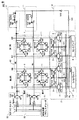
FIG. 4 is a diagram illustrating the configuration of the semiconductor device according to the third embodiment.
図4の半導体装置200が、図2の半導体装置100と相違する点について説明する。
アシスト制御回路12は、2段のインバータIV4,IV5を備える。
The difference between the
The
制御回路・アドレスデコーダ21は、信号配線LAを通じて、制御信号パルスPLをアシスト制御回路12およびアシストドライバ11へ伝送する。信号配線LAは、半導体装置200が実装される基板に水平な方向において、メモリアレイ62の外側に設けられる。
The control circuit /
IV4は、制御回路・アドレスデコーダ21から制御信号パルスPLを受ける。インバータIV5は、インバータIV4の出力を受ける。
IV4 receives a control signal pulse PL from the control circuit /
アシストドライバ11は、NAND回路NAN2と、PMOSトランジスタP8とを含む。
The
PMOSトランジスタP8は、ワード線WLの末端Yと、電源Vddとの間に設けられる。本実施の形態では、PMOSトランジスタP8は、ワード線WLの立ち上がり時に、ワード線WLの末端Yの電圧が所定値まで増加するとオンとなり、ワード線WLの立下り時に、制御回路・アドレスデコーダ21からの制御信号によってオフとなる。
The PMOS transistor P8 is provided between the terminal Y of the word line WL and the power supply Vdd. In the present embodiment, the PMOS transistor P8 is turned on when the voltage at the terminal Y of the word line WL increases to a predetermined value when the word line WL rises, and from the control circuit /
NAND回路NAN2の一方の入力は、ワード線WLの末端Yに接続され、他方の入力は、インバータIV5に接続される。NAND回路NAN2の出力は、PMOSトランジスタP8のゲートに接続される。 One input of the NAND circuit NAN2 is connected to the terminal Y of the word line WL, and the other input is connected to the inverter IV5. The output of the NAND circuit NAN2 is connected to the gate of the PMOS transistor P8.
制御回路・アドレスデコーダ21から出力されて、インバータIV4およびIV5を経由して、NAND回路NAN2に入力される制御信号パルスPLは、ワード線WLの立ち上がり開始からワード線WLの末端Yの電圧がVddに達するまでの間はハイレベルであり、ワード線WLの立ち下がり開始からワード線WLの末端Yの電圧が接地電圧(0V)に達するまでの間はロウレベルである。
The control signal pulse PL output from the control circuit /
図5は、第3の実施形態におけるワード線WLの先端、末端、およびアシストドライバ11内の電圧の変化を表わす図である。
FIG. 5 is a diagram illustrating changes in the voltage at the tip and end of the word line WL and in the
時刻t0において、NAND回路NAN2の入力端子Wは、制御回路・アドレスデコーダ21から出力された制御信号パルスPLを受けて、入力端子Wの電圧が立ち上がる。
At time t0, the input terminal W of the NAND circuit NAN2 receives the control signal pulse PL output from the control circuit /
時刻t1において、選択された行のワード線ドライバ22によってワード線WLの先端Xが電源Vddに接続されると、ワード線WLの先端Xの電圧は、(1)に示すように、比較的早い速度で立ち上がるが、ワード線WLの末端Yの電圧は、(2)に示すように、比較的遅い速度で立ち上がる。
When the tip X of the word line WL is connected to the power supply Vdd by the
時刻t2において、ワード線WLの末端Yの電圧が十分に高くなってNAND回路NAN2を構成するインバータの閾値を超えると、アシストドライバ10内のNAND回路NAN2の出力端子Zの電圧は、ロウレベルとなる。これによって、アシストドライバ10内のPMOSトランジスタP8がオンとなる。その結果、電源Vddがワード線WLの末端Yと接続されて、(3)に示すように、末端Yでの電圧の立ち上がりが加速される。
At time t2, when the voltage at the terminal Y of the word line WL becomes sufficiently high and exceeds the threshold value of the inverter constituting the NAND circuit NAN2, the voltage at the output terminal Z of the NAND circuit NAN2 in the
時刻t3において、NAND回路NAN2の入力端子Wにおいて、制御信号パルスPLが立ち下がると、NAND回路NAN2の出力端子Zの電圧は、ハイレベルとなる。これによって、PMOSトランジスタP8がオフとなる。その結果、電源Vddとワード線WLの末端Yとの接続が分断される。 At time t3, when the control signal pulse PL falls at the input terminal W of the NAND circuit NAN2, the voltage at the output terminal Z of the NAND circuit NAN2 becomes high level. As a result, the PMOS transistor P8 is turned off. As a result, the connection between the power supply Vdd and the terminal Y of the word line WL is disconnected.
時刻t4において、選択された行が非選択に変化して、ワード線ドライバ22によってワード線WLの先端Xがグランドに接続されると、ワード線WLの先端Xの電圧は、(4)に示すように、比較的早い速度で立ち下がる。PMOSトランジスタP8が既にオフとされているため、ワード線WLの末端Yの電圧も、(5)に示すように比較的早い速度で立ち下がる。
When the selected row changes to non-selected at time t4 and the
第2の実施形態では、ワード線WLの非活性化時にアシストドライバ10内のプルアップ用のPMOSトランジスタP8と、ワード線ドライバ22を構成するNMOSトランジスタN7とが両方オンとなる期間が存在するため、図3の(5)に示すように、末端Yの電圧が低下する速度が遅くなった。
In the second embodiment, there is a period during which both the pull-up PMOS transistor P8 in the
これに対して、本実施の形態では、プルアップ用のPMOSトランジスタP8と、ワード線ドライバ22を構成するNMOSトランジスタN7とが両方オンとなる期間がないので、図5の(5)に示すように、末端Yの電圧が先端Xと同様の速度で低下する。その結果、ワード線WLの非活性化時の高速化および低電力化を図ることができる。
On the other hand, in the present embodiment, there is no period in which both the pull-up PMOS transistor P8 and the NMOS transistor N7 constituting the
ワード線WLは、メモリセル1が配置される領域の真上の半導体層に配置されるので、ワード線WLを太くする設計は、困難である。これに対して、本実施の形態によれば、制御回路・アドレスデコーダ21から出力される制御信号パルスPLは、メモリアレイ62の外側に配置される信号配線LAを通じて、アシスト制御回路12およびアシストドライバ11へ伝送されるので、ワード線WLのようにレイアウト上の制約を受けることなく太幅化などによって低抵抗化することができる。
Since the word line WL is disposed in the semiconductor layer immediately above the region where the
[第4の実施形態]
図6は、第4の実施形態の半導体装置の構成を表わす図である。
[Fourth Embodiment]
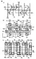
FIG. 6 is a diagram illustrating the configuration of the semiconductor device of the fourth embodiment.
図6の半導体装置300が、図2の半導体装置100と相違する点について説明する。
アシストドライバ13は、NAND回路NAN3と、PMOSトランジスタP8と、遅延回路DLとを備える。遅延回路DLは、3段のインバータIV6,IV7,IV8を含む。
The difference between the
The
インバータIV6の入力は、ワード線WLの末端Yに接続され、インバータIV7の入力は、インバータIV6の出力に接続され、インバータIV8の入力は、インバータIV7の入力に接続される。 The input of inverter IV6 is connected to terminal Y of word line WL, the input of inverter IV7 is connected to the output of inverter IV6, and the input of inverter IV8 is connected to the input of inverter IV7.
PMOSトランジスタP8は、ワード線WLの末端Yと、電源Vddとの間に設けられる。PMOSトランジスタP8は、ワード線WLの立ち上がり時に、ワード線WLの末端Yの電圧が所定値まで立ち上がった時から所定時間だけロウレベルとなるワンショットパルスによって、オンとなる。 The PMOS transistor P8 is provided between the terminal Y of the word line WL and the power supply Vdd. The PMOS transistor P8 is turned on by a one-shot pulse that goes low for a predetermined time from the time when the voltage at the terminal Y of the word line WL rises to a predetermined value when the word line WL rises.
NAND回路NAN3の一方の入力は、ワード線WLの末端Yに接続され、他方の入力は、インバータIV8の出力に接続される。NAND回路NAN3の出力は、PMOSトランジスタP8のゲートに接続される。 One input of the NAND circuit NAN3 is connected to the terminal Y of the word line WL, and the other input is connected to the output of the inverter IV8. The output of the NAND circuit NAN3 is connected to the gate of the PMOS transistor P8.
図7は、第4の実施形態における、ワード線WLの先端、末端、およびアシストドライバ13内の電圧の変化を表わす図である。
FIG. 7 is a diagram illustrating a change in voltage in the tip and end of the word line WL and in the
時刻t1において、選択された行のワード線ドライバ22によってワード線WLの先端Xが電源Vddに接続されると、ワード線WLの先端Xの電圧は、(1)に示すように、比較的早い速度で立ち上がるが、ワード線WLの末端Yの電圧は、(2)に示すように、比較的遅い速度で立ち上がる。
When the tip X of the word line WL is connected to the power supply Vdd by the
時刻t2において、ワード線WLの末端Yの電圧が十分高くなって、インバータIV6の閾値を超えると、遅延回路DLおよびNAND回路NAN3によって、(3)に示すように、時刻t2から遅延回路DLによる遅延時間dtの間、NAND回路NAN3の出力端子Yの電圧がロウレベルとなるワンショットパルスが生成される。これによって、アシストドライバ10内のPMOSトランジスタP8がオンとなる。その結果、電源Vddがワード線WLの末端Yと接続されて、(3)に示すように、末端Yでの電圧の立ち上がりが加速される。
When the voltage at the terminal Y of the word line WL becomes sufficiently high at time t2 and exceeds the threshold value of the inverter IV6, the delay circuit DL and the NAND circuit NAN3 cause the delay circuit DL to start from time t2 as shown in (3). During the delay time dt, a one-shot pulse is generated in which the voltage at the output terminal Y of the NAND circuit NAN3 becomes low level. As a result, the PMOS transistor P8 in the
時刻t3において、ワンショットパルスが終了し、端子Zの電圧がハイレベルとなると、アシストドライバ10内のPMOSトランジスタP8がオフとなる。その結果、電源Vddとワード線WLの末端Yとの接続が分断される。
At time t3, when the one-shot pulse ends and the voltage at the terminal Z becomes high level, the PMOS transistor P8 in the
時刻t4において、選択された行が非選択に変化して、ワード線ドライバ22によってワード線WLの先端Xがグランドに接続されると、ワード線WLの先端Xの電圧は、(4)に示すように、比較的早い速度で立ち下がる。PMOSトランジスタP8が既にオフとされているため、ワード線WLの末端Yの電圧も、(5)に示すように比較的早い速度で立ち下がる。
When the selected row changes to non-selected at time t4 and the
以上のように、本実施の形態によれば、第3の実施形態と同様に、第2の実施形態で見られる、ワード線WLの非活性化時にアシストドライバ10内のプルアップ用PMOSトランジスタP8と、ワード線ドライバ22を構成するNMOSトランジスタN7とが同時にオンすることがなくなる。その結果、ワード線WLの非活性化時の高速化および低電力化が図れる。
As described above, according to the present embodiment, similarly to the third embodiment, the pull-up PMOS transistor P8 in the
また、本実施の形態によれば、第3の実施形態のように、制御回路・アドレスデコーダ21から制御信号パルスPLを出力する必要がないので、タイミング設計の自由度が上がる。
Further, according to the present embodiment, it is not necessary to output the control signal pulse PL from the control circuit /
[第5の実施形態]
上述の実施形態のメモリセル1は、縦長型メモリセルである。本実施の形態の半導体装置は、メモリセルとして、横長型メモリセルを含む。
[Fifth Embodiment]
The
本実施の形態のメモリセルMCは、上述の実施形態のメモリセル1と同様に、負荷トランジスタ(PチャネルMOSトランジスタ)41,42、ドライバトランジスタ(NチャネルMOSトランジスタ)43,44およびアクセストランジスタ(NチャネルMOSトランジスタ)45,46を含む。このメモリセル500は、トランジスタ41〜46などのレイアウトがメモリセル1と異なる。
Similarly to the
すなわち、横長型メモリセルMCは、図8(b)に示すように、1つのN型ウェルNWとその両側に配置されたP型ウェルPW,PWの表面に形成される。まず、N型ウェルNWから一方のP型ウェルPWにわたって図中X方向に延在するゲート電極GE1と、N型ウェルNWから他方のP型ウェルPWにわたって図中X方向に延在するゲート電極GE2と、一方のP型ウェルPW上に図中X方向に延在するゲート電極GE3と、他方のP型ウェルPW上に図中X方向に延在するゲート電極GE4とがポリシリコン層によって形成される。 That is, the horizontally long memory cell MC is formed on the surface of one N-type well NW and P-type wells PW and PW arranged on both sides thereof, as shown in FIG. 8B. First, a gate electrode GE1 extending in the X direction from the N type well NW to one P type well PW, and a gate electrode GE2 extending from the N type well NW to the other P type well PW in the X direction in the drawing. A gate electrode GE3 extending in the X direction in the drawing on one P-type well PW and a gate electrode GE4 extending in the X direction in the drawing on the other P-type well PW are formed by a polysilicon layer. The
次いで、一方のP型ウェルPWにおいてゲート電極GE1,GE3を横切るようにしてN型活性層NA1が形成され、他方のP型ウェルPWにおいてゲート電極GE2,GE4を横切るようにしてN型活性層NA2が形成され、N型ウェルNWにおいてそれぞれゲート電極GE1,GE2を横切るようにしてP型活性層PA1,PA2が形成される。 Next, an N-type active layer NA1 is formed across the gate electrodes GE1 and GE3 in one P-type well PW, and an N-type active layer NA2 across the gate electrodes GE2 and GE4 in the other P-type well PW. P-type active layers PA1 and PA2 are formed in the N-type well NW so as to cross the gate electrodes GE1 and GE2, respectively.
ゲート電極GE1とP型活性層PA1、ゲート電極GE2とP型活性層PA2は、それぞれPチャネルMOSトランジスタ41,42を構成する。ゲート電極GE1とN型活性層NA1、ゲート電極GE3とN型活性層NA1は、それぞれNチャネルMOSトランジスタ43,45を構成する。ゲート電極GE2とN型活性層NA2、ゲート電極GE4とN型活性層NA2は、それぞれNチャネルMOSトランジスタ44,46を構成する。
The gate electrode GE1 and the P-type active layer PA1, and the gate electrode GE2 and the P-type active layer PA2 constitute P-
次に、N型活性層NA1の中央部、P型活性層PA1の一方端部およびゲート電極GE2の一方端部にわたってローカル配線LL1が形成されるとともに、N型活性層NA2の中央部、P型活性層PA1の一方端部およびゲート電極GE1の一方端部にわたってローカル配線LL2が形成される。図8(b)において、ローカル配線LL1と活性層NA1,PA1とが重なっている部分は導通している。ローカル配線LL2と活性層NA2,PA2とが重なっている部分は導通している。ゲート電極GE2とローカル配線LL1、ゲート電極GE1とローカル配線LL2は、それぞれコンタクトホールCH,CHを介して互いに接続される。 Next, a local wiring LL1 is formed across the central portion of the N-type active layer NA1, one end portion of the P-type active layer PA1, and one end portion of the gate electrode GE2, and the central portion of the N-type active layer NA2 A local wiring LL2 is formed across one end of the active layer PA1 and one end of the gate electrode GE1. In FIG. 8B, the portion where the local wiring LL1 and the active layers NA1 and PA1 overlap is conductive. The portion where the local wiring LL2 and the active layers NA2 and PA2 overlap is conductive. The gate electrode GE2 and the local wiring LL1, and the gate electrode GE1 and the local wiring LL2 are connected to each other through contact holes CH and CH, respectively.
次に、図8(c)に示すように、図中X方向に延在する複数のメタル配線MLが第1アルミ配線層によって形成され、さらにその上方に、図中Y方向に延在するメモリセル接地配線MGL、ビット線BL、メモリセル電源配線MVL、ビット線/BLおよびメモリセル接地配線MGLが第2アルミ配線層によって形成される。複数のメタル配線MLのうちメモリセルMCの中央部を横切るメタル配線は、ワード線WLとなる。 Next, as shown in FIG. 8C, a plurality of metal wirings ML extending in the X direction in the figure are formed by the first aluminum wiring layer, and further above the memory extending in the Y direction in the figure. Cell ground wiring MGL, bit line BL, memory cell power supply wiring MVL, bit line / BL and memory cell ground wiring MGL are formed by the second aluminum wiring layer. Of the plurality of metal wirings ML, the metal wiring crossing the central portion of the memory cell MC becomes the word line WL.
P型活性層PA1の一方端部(PチャネルMOSトランジスタ41のソース)は、コンタクトホールCH、メタル配線MLおよびビアホールVHを介してメモリセル電源配線MVLに接続される。P型活性層PA2の一方端部(PチャネルMOSトランジスタ42のソース)は、コンタクトホールCH、メタル配線MLおよびビアホールVHを介してメモリセル電源配線MVLに接続される。 One end portion of P-type active layer PA1 (the source of P-channel MOS transistor 41) is connected to memory cell power supply wiring MVL through contact hole CH, metal wiring ML, and via hole VH. One end portion of P-type active layer PA2 (the source of P-channel MOS transistor 42) is connected to memory cell power supply wiring MVL through contact hole CH, metal wiring ML, and via hole VH.
N型活性層NA1の一方端部(NチャネルMOSトランジスタ43のソース)は、コンタクトホールCH、メタル配線MLおよびビアホールVHを介してメモリセル接地配線MGLに接続される。N型活性層NA2の一方端部(NチャネルMOSトランジスタ44のソース)は、コンタクトホールCH、メタル配線MLおよびビアホールVHを介してメモリセル接地配線MGLに接続される。 One end of N-type active layer NA1 (the source of N-channel MOS transistor 43) is connected to memory cell ground wiring MGL via contact hole CH, metal wiring ML, and via hole VH. One end of N-type active layer NA2 (the source of N-channel MOS transistor 44) is connected to memory cell ground wiring MGL via contact hole CH, metal wiring ML, and via hole VH.
N型活性層NA1の他方端部(NチャネルMOSトランジスタ45のドレイン)は、コンタクトホールCH、メタル配線MLおよびビアホールVHを介してビット線BLに接続される。N型活性層NA2の他方端部(NチャネルMOSトランジスタ46のドレイン)は、コンタクトホールCH、メタル配線MLおよびビアホールVHを介してビット線/BLに接続される。ゲート電極GE3,GE4は、それぞれコンタクトホールCHを介してワード線WLに接続される。 The other end of N-type active layer NA1 (the drain of N-channel MOS transistor 45) is connected to bit line BL via contact hole CH, metal interconnection ML, and via hole VH. The other end of N-type active layer NA2 (the drain of N-channel MOS transistor 46) is connected to bit line / BL via contact hole CH, metal interconnection ML, and via hole VH. Gate electrodes GE3 and GE4 are each connected to word line WL through contact hole CH.
本実施の形態では、メモリセルMCは、上述のように横長型のため、本実施の形態のワード線WLが長くなる。ワード線WLが長いと、ワード線WLの活性化時において、ワード線ドライバ22に近い箇所の電圧の立ち上がりに比べて、ワード線ドライバ22から遠い箇所の電圧の立ち上がり速度が遅いという問題が顕著になる。
In the present embodiment, since the memory cell MC is horizontally long as described above, the word line WL of the present embodiment becomes long. If the word line WL is long, when the word line WL is activated, the rise of the voltage at a location far from the
本実施の形態の半導体装置が、第1〜第4の実施形態で説明したアシストドライバ10,11,13を備えることによって、この問題を回避することができる。
This problem can be avoided when the semiconductor device of the present embodiment includes the
上述の実施形態では、ライトドライバ5およびセンスアンプ6は、隣接する2つの列ごとに設けられ、隣接する2つの列のビット線対BT,BBと接続することとしたが、これに限定するものではない。ライトドライバ5およびセンスアンプ6が隣接する3つ以上の列ごとに設けられ、隣接する3つ以上の列のビット線対BT,BBと接続するものとしてもよい。
In the above-described embodiment, the
以上、本発明者によってなされた発明を実施の形態に基づき具体的に説明したが、本発明は実施の形態に限定されるものではなく、その要旨を逸脱しない範囲で種々変更可能であることはいうまでもない。 As mentioned above, the invention made by the present inventor has been specifically described based on the embodiment. However, the present invention is not limited to the embodiment, and various modifications can be made without departing from the scope of the invention. Needless to say.
1,500,MC メモリセル、3 プリチャージ回路、4 カラムセレクタ、5 ライドドライバ、6 センスアンプ、10,11,13 アシストドライバ、21 制御回路・アドレスデコーダ、22,502 ワード線ドライバ、62,98 メモリアレイ、100,200,300,1000 半導体装置、BT,BB ビット線、WL ワード線、NAN1〜NAN3 NAND回路、IV1〜IV8 インバータ、P1〜P8,P20,41,42 PMOSトランジスタ、N1〜N8,N20,N21,43〜46 NMOSトランジスタ、NW ウェル、MVK メモリセル電源配線、MGL メモリセル接地配線。 1,500, MC memory cell, 3 precharge circuit, 4 column selector, 5 ride driver, 6 sense amplifier, 10, 11, 13 assist driver, 21 control circuit / address decoder, 22,502 word line driver, 62,98 Memory array, 100, 200, 300, 1000 Semiconductor device, BT, BB bit line, WL word line, NAN1-NAN3 NAND circuit, IV1-IV8 inverter, P1-P8, P20, 41, 42 PMOS transistor, N1-N8, N20, N21, 43 to 46 NMOS transistor, NW well, MVK memory cell power supply wiring, MGL memory cell ground wiring.
Claims (11)
前記メモリアレイの各行に対応して設けられたワード線と、
前記ワード線の一端に接続されて、対応する行が選択されたときに、前記ワード線の一端を第1の電源に接続することによってワード線を活性化するワード線ドライバと、
前記ワード線の他端に接続されて、前記ワード線の他端の電圧に応じて、前記ワード線の他端を前記第1の電源に接続するアシストドライバと、
を備え、
前記アシストドライバは、
前記第1の電源と前記ワード線の他端との間に設けられたPMOSトランジスタと、
前記ワード線の他端に接続された遅延回路と、
一方の入力が前記ワード線の他端に接続され、他方の入力が前記遅延回路の出力を受け、出力が前記PMOSトランジスタのゲートに接続されたNAND回路と、
を含む、半導体装置。 A memory array including a plurality of memory cells arranged in a matrix;
A word line provided corresponding to each row of the memory array;
A word line driver that is connected to one end of the word line and activates the word line by connecting one end of the word line to a first power supply when a corresponding row is selected;
An assist driver connected to the other end of the word line and connecting the other end of the word line to the first power supply according to a voltage at the other end of the word line ;
Bei to give a,
The assist driver is
A PMOS transistor provided between the first power source and the other end of the word line;
A delay circuit connected to the other end of the word line;
A NAND circuit having one input connected to the other end of the word line, the other input receiving the output of the delay circuit, and an output connected to the gate of the PMOS transistor;
Including a semiconductor device.
隣接する複数の列のビット線対と接続され、前記メモリセルへのデータの書込み時に、前記隣接する複数の列のうちの選択された列のビット線対へ書込みデータに応じた電圧を出力する、請求項1記載の半導体装置。 A bit line pair provided corresponding to each column of the memory array;
Connected to the bit line pairs of a plurality of adjacent columns, and outputs a voltage corresponding to the write data to the bit line pair of a selected column among the plurality of adjacent columns when data is written to the memory cell. The semiconductor device according to claim 1.
隣接する複数の列のビット線対と接続され、前記メモリセルからのデータの読出し時に、前記隣接する複数の列のうちの選択された列のビット線対の電圧を増幅するセンスアンプとを備える、請求項1記載の半導体装置。 A bit line pair provided corresponding to each column of the memory array;
A sense amplifier connected to a bit line pair of a plurality of adjacent columns and amplifying a voltage of a bit line pair of a selected column among the plurality of adjacent columns when reading data from the memory cell; The semiconductor device according to claim 1.
前記メモリアレイの各行に対応して設けられたワード線と、
前記ワード線の一端に接続されて、対応する行が選択されたときに、前記ワード線の一端を第1の電源に接続するワード線ドライバと、
前記第1の電源と前記ワード線の他端との間に設けられたPMOSトランジスタと、
前記ワード線の他端に接続された遅延回路と、
一方の入力が前記ワード線の他端に接続され、他方の入力が前記遅延回路の出力を受け、出力が前記PMOSトランジスタのゲートに接続されたNAND回路と、
を備え、
前記PMOSトランジスタは、前記ワード線の立ち上がり時に、前記ワード線の他端の電圧が所定値まで増加するとオンとなり、前記ワード線の立下り時に、制御信号によってオフとなる、半導体装置。 A memory array including a plurality of memory cells arranged in a matrix;
A word line provided corresponding to each row of the memory array;
A word line driver connected to one end of the word line and connecting one end of the word line to a first power supply when a corresponding row is selected;
A PMOS transistor provided between the first power source and the other end of the word line;
A delay circuit connected to the other end of the word line;
A NAND circuit having one input connected to the other end of the word line, the other input receiving the output of the delay circuit, and an output connected to the gate of the PMOS transistor;
With
The PMOS transistor is turned on when the voltage at the other end of the word line increases to a predetermined value when the word line rises, and turned off by a control signal when the word line falls.
前記メモリアレイの各行に対応して設けられたワード線と、
前記ワード線の一端に接続されて、対応する行が選択されたときに、前記ワード線の一端を第1の電源に接続するワード線ドライバと、
前記第1の電源と前記ワード線の他端との間に設けられたPMOSトランジスタと、
前記ワード線の他端に接続された遅延回路と、
一方の入力が前記ワード線の他端に接続され、他方の入力が前記遅延回路の出力を受け、出力が前記PMOSトランジスタのゲートに接続されたNAND回路と、
を備え、
前記PMOSトランジスタは、前記ワード線の立ち上がり時に、前記ワード線の他端の電圧が所定値まで立ち上がった時から所定時間だけロウレベルとなるワンショットパルスによって、オンとなる、半導体装置。 A memory array including a plurality of memory cells arranged in a matrix;
A word line provided corresponding to each row of the memory array;
A word line driver connected to one end of the word line and connecting one end of the word line to a first power supply when a corresponding row is selected;
A PMOS transistor provided between the first power source and the other end of the word line;
A delay circuit connected to the other end of the word line ;
A NAND circuit having one input connected to the other end of the word line, the other input receiving the output of the delay circuit, and an output connected to the gate of the PMOS transistor;
With
The PMOS transistor is turned on by a one-shot pulse that is at a low level for a predetermined time after the voltage at the other end of the word line rises to a predetermined value when the word line rises.
Priority Applications (5)
| Application Number | Priority Date | Filing Date | Title |
|---|---|---|---|
| JP2015179683A JP6469554B2 (en) | 2015-09-11 | 2015-09-11 | Semiconductor device |
| US15/212,162 US9721647B2 (en) | 2015-09-11 | 2016-07-15 | Semiconductor device |
| CN201610704791.5A CN106531206B (en) | 2015-09-11 | 2016-08-22 | Semiconductor device with a plurality of transistors |
| US15/627,535 US10255970B2 (en) | 2015-09-11 | 2017-06-20 | Semiconductor device |
| US16/145,342 US10354722B2 (en) | 2015-09-11 | 2018-09-28 | Semiconductor device |
Applications Claiming Priority (1)
| Application Number | Priority Date | Filing Date | Title |
|---|---|---|---|
| JP2015179683A JP6469554B2 (en) | 2015-09-11 | 2015-09-11 | Semiconductor device |
Publications (3)
| Publication Number | Publication Date |
|---|---|
| JP2017054570A JP2017054570A (en) | 2017-03-16 |
| JP2017054570A5 JP2017054570A5 (en) | 2018-06-28 |
| JP6469554B2 true JP6469554B2 (en) | 2019-02-13 |
Family
ID=58238935
Family Applications (1)
| Application Number | Title | Priority Date | Filing Date |
|---|---|---|---|
| JP2015179683A Active JP6469554B2 (en) | 2015-09-11 | 2015-09-11 | Semiconductor device |
Country Status (3)
| Country | Link |
|---|---|
| US (3) | US9721647B2 (en) |
| JP (1) | JP6469554B2 (en) |
| CN (1) | CN106531206B (en) |
Families Citing this family (8)
| Publication number | Priority date | Publication date | Assignee | Title |
|---|---|---|---|---|
| JP6469554B2 (en) * | 2015-09-11 | 2019-02-13 | ルネサスエレクトロニクス株式会社 | Semiconductor device |
| US9786363B1 (en) * | 2016-11-01 | 2017-10-10 | Taiwan Semiconductor Manufacturing Co., Ltd. | Word-line enable pulse generator, SRAM and method for adjusting word-line enable time of SRAM |
| US10943645B2 (en) * | 2018-07-31 | 2021-03-09 | Taiwan Semiconductor Manufacturing Company, Ltd | Memory device with a booster word line |
| JP7270451B2 (en) * | 2019-04-26 | 2023-05-10 | ルネサスエレクトロニクス株式会社 | Semiconductor device and method for driving semiconductor device |
| JP2021108307A (en) * | 2019-12-27 | 2021-07-29 | キオクシア株式会社 | Semiconductor storage |
| US11170830B2 (en) * | 2020-02-11 | 2021-11-09 | Taiwan Semiconductor Manufacturing Company Limited | Word line driver for low voltage operation |
| KR20220058284A (en) | 2020-10-30 | 2022-05-09 | 삼성전자주식회사 | Integrated circuit including cell array with word line assist cells |
| US11521670B2 (en) * | 2020-11-12 | 2022-12-06 | Micron Technology, Inc. | Word lines coupled to pull-down transistors, and related devices, systems, and methods |
Family Cites Families (15)
| Publication number | Priority date | Publication date | Assignee | Title |
|---|---|---|---|---|
| JPS55150189A (en) * | 1979-05-10 | 1980-11-21 | Nec Corp | Memory circuit |
| JPS60226095A (en) * | 1984-04-25 | 1985-11-11 | Hitachi Micro Comput Eng Ltd | Semiconductor storage device |
| JPS63276793A (en) * | 1987-05-07 | 1988-11-15 | Nec Ic Microcomput Syst Ltd | Word line driving circuit |
| JPH06203579A (en) * | 1993-01-08 | 1994-07-22 | Fujitsu Ltd | Output circuit and memory device |
| JP3908493B2 (en) * | 2001-08-30 | 2007-04-25 | 株式会社東芝 | Electronic circuit and semiconductor memory device |
| JP4439167B2 (en) * | 2002-08-30 | 2010-03-24 | 株式会社ルネサステクノロジ | Semiconductor memory device |
| US7064981B2 (en) * | 2004-08-04 | 2006-06-20 | Micron Technology, Inc. | NAND string wordline delay reduction |
| JP4912016B2 (en) * | 2005-05-23 | 2012-04-04 | ルネサスエレクトロニクス株式会社 | Semiconductor memory device |
| JP4631743B2 (en) * | 2006-02-27 | 2011-02-16 | ソニー株式会社 | Semiconductor device |
| US7379354B2 (en) * | 2006-05-16 | 2008-05-27 | Texas Instruments Incorporated | Methods and apparatus to provide voltage control for SRAM write assist circuits |
| US7733686B2 (en) * | 2006-12-30 | 2010-06-08 | Texas Instruments Incorporated | Pulse width control for read and write assist for SRAM circuits |
| US8014226B2 (en) * | 2009-12-22 | 2011-09-06 | Arm Limited | Integrated circuit memory with word line driving helper circuits |
| JP2014067942A (en) * | 2012-09-27 | 2014-04-17 | Toshiba Corp | Non volatile semiconductor storage device |
| JP2014099225A (en) | 2012-11-14 | 2014-05-29 | Renesas Electronics Corp | Semiconductor device |
| JP6469554B2 (en) * | 2015-09-11 | 2019-02-13 | ルネサスエレクトロニクス株式会社 | Semiconductor device |
-
2015
- 2015-09-11 JP JP2015179683A patent/JP6469554B2/en active Active
-
2016
- 2016-07-15 US US15/212,162 patent/US9721647B2/en active Active
- 2016-08-22 CN CN201610704791.5A patent/CN106531206B/en active Active
-
2017
- 2017-06-20 US US15/627,535 patent/US10255970B2/en active Active
-
2018
- 2018-09-28 US US16/145,342 patent/US10354722B2/en active Active
Also Published As
| Publication number | Publication date |
|---|---|
| US10255970B2 (en) | 2019-04-09 |
| US20170287553A1 (en) | 2017-10-05 |
| JP2017054570A (en) | 2017-03-16 |
| CN106531206B (en) | 2022-05-27 |
| US10354722B2 (en) | 2019-07-16 |
| US9721647B2 (en) | 2017-08-01 |
| CN106531206A (en) | 2017-03-22 |
| US20190035456A1 (en) | 2019-01-31 |
| US20170076785A1 (en) | 2017-03-16 |
Similar Documents
| Publication | Publication Date | Title |
|---|---|---|
| JP6469554B2 (en) | Semiconductor device | |
| JP4553185B2 (en) | Semiconductor integrated circuit device | |
| US7697320B2 (en) | Semiconductor memory device | |
| TWI415126B (en) | Semiconductor memory | |
| JP2009070480A (en) | Semiconductor storage device | |
| JP4598420B2 (en) | Semiconductor memory device and timing control method | |
| US20130258794A1 (en) | Memory device having control circuitry for sense amplifier reaction time tracking | |
| US8144523B2 (en) | Semiconductor storage device | |
| JP2012128895A (en) | Semiconductor memory device | |
| JP2008219232A5 (en) | ||
| JP4245147B2 (en) | Hierarchical word line type semiconductor memory device and sub word driver circuit used therefor | |
| US7489581B2 (en) | Semiconductor memory | |
| JP5586038B2 (en) | Semiconductor integrated circuit device | |
| JP5456571B2 (en) | Semiconductor integrated circuit device | |
| JP5867275B2 (en) | Semiconductor memory device and data writing method thereof | |
| US8125820B2 (en) | Semiconductor memory device | |
| TWI751845B (en) | Memory device and method for operating memory device | |
| US20230282274A1 (en) | Memory device and method of operating the same | |
| JP7270451B2 (en) | Semiconductor device and method for driving semiconductor device | |
| JP2015111489A (en) | Semiconductor integrated circuit device | |
| JP2013041663A (en) | Semiconductor integrated circuit device | |
| JP2014139860A (en) | Semiconductor integrated circuit device | |
| JP2006085785A (en) | Semiconductor integrated circuit apparatus |
Legal Events
| Date | Code | Title | Description |
|---|---|---|---|
| A521 | Request for written amendment filed |
Free format text: JAPANESE INTERMEDIATE CODE: A523 Effective date: 20180514 |
|
| A621 | Written request for application examination |
Free format text: JAPANESE INTERMEDIATE CODE: A621 Effective date: 20180514 |
|
| A977 | Report on retrieval |
Free format text: JAPANESE INTERMEDIATE CODE: A971007 Effective date: 20180919 |
|
| A131 | Notification of reasons for refusal |
Free format text: JAPANESE INTERMEDIATE CODE: A131 Effective date: 20181002 |
|
| A521 | Request for written amendment filed |
Free format text: JAPANESE INTERMEDIATE CODE: A523 Effective date: 20181203 |
|
| TRDD | Decision of grant or rejection written | ||
| A01 | Written decision to grant a patent or to grant a registration (utility model) |
Free format text: JAPANESE INTERMEDIATE CODE: A01 Effective date: 20181218 |
|
| A61 | First payment of annual fees (during grant procedure) |
Free format text: JAPANESE INTERMEDIATE CODE: A61 Effective date: 20190116 |
|
| R150 | Certificate of patent or registration of utility model |
Ref document number: 6469554 Country of ref document: JP Free format text: JAPANESE INTERMEDIATE CODE: R150 |