JP6385899B2 - TEM sample mounting structure - Google Patents
TEM sample mounting structure Download PDFInfo
- Publication number
- JP6385899B2 JP6385899B2 JP2015142246A JP2015142246A JP6385899B2 JP 6385899 B2 JP6385899 B2 JP 6385899B2 JP 2015142246 A JP2015142246 A JP 2015142246A JP 2015142246 A JP2015142246 A JP 2015142246A JP 6385899 B2 JP6385899 B2 JP 6385899B2
- Authority
- JP
- Japan
- Prior art keywords
- sample
- rotating
- needle
- orthogonal
- angles
- Prior art date
- Legal status (The legal status is an assumption and is not a legal conclusion. Google has not performed a legal analysis and makes no representation as to the accuracy of the status listed.)
- Expired - Fee Related
Links
Images


Classifications
-
- H—ELECTRICITY
- H01—ELECTRIC ELEMENTS
- H01J—ELECTRIC DISCHARGE TUBES OR DISCHARGE LAMPS
- H01J37/00—Discharge tubes with provision for introducing objects or material to be exposed to the discharge, e.g. for the purpose of examination or processing thereof
- H01J37/02—Details
- H01J37/22—Optical or photographic arrangements associated with the tube
-
- H—ELECTRICITY
- H01—ELECTRIC ELEMENTS
- H01J—ELECTRIC DISCHARGE TUBES OR DISCHARGE LAMPS
- H01J2237/00—Discharge tubes exposing object to beam, e.g. for analysis treatment, etching, imaging
- H01J2237/20—Positioning, supporting, modifying or maintaining the physical state of objects being observed or treated
- H01J2237/202—Movement
- H01J2237/20207—Tilt
-
- H—ELECTRICITY
- H01—ELECTRIC ELEMENTS
- H01J—ELECTRIC DISCHARGE TUBES OR DISCHARGE LAMPS
- H01J2237/00—Discharge tubes exposing object to beam, e.g. for analysis treatment, etching, imaging
- H01J2237/20—Positioning, supporting, modifying or maintaining the physical state of objects being observed or treated
- H01J2237/202—Movement
- H01J2237/20214—Rotation
-
- H—ELECTRICITY
- H01—ELECTRIC ELEMENTS
- H01J—ELECTRIC DISCHARGE TUBES OR DISCHARGE LAMPS
- H01J2237/00—Discharge tubes exposing object to beam, e.g. for analysis treatment, etching, imaging
- H01J2237/22—Treatment of data
- H01J2237/226—Image reconstruction
-
- H—ELECTRICITY
- H01—ELECTRIC ELEMENTS
- H01J—ELECTRIC DISCHARGE TUBES OR DISCHARGE LAMPS
- H01J37/00—Discharge tubes with provision for introducing objects or material to be exposed to the discharge, e.g. for the purpose of examination or processing thereof
- H01J37/02—Details
- H01J37/20—Means for supporting or positioning the objects or the material; Means for adjusting diaphragms or lenses associated with the support
-
- H—ELECTRICITY
- H01—ELECTRIC ELEMENTS
- H01J—ELECTRIC DISCHARGE TUBES OR DISCHARGE LAMPS
- H01J37/00—Discharge tubes with provision for introducing objects or material to be exposed to the discharge, e.g. for the purpose of examination or processing thereof
- H01J37/02—Details
- H01J37/244—Detectors; Associated components or circuits therefor
-
- H—ELECTRICITY
- H01—ELECTRIC ELEMENTS
- H01J—ELECTRIC DISCHARGE TUBES OR DISCHARGE LAMPS
- H01J37/00—Discharge tubes with provision for introducing objects or material to be exposed to the discharge, e.g. for the purpose of examination or processing thereof
- H01J37/26—Electron or ion microscopes; Electron or ion diffraction tubes
Description
本発明は、透過電子顕微鏡分析のための方法、および取り付けられた試料の直交画像を得るための方法に関する。 The present invention relates to a method for transmission electron microscopy analysis and a method for obtaining an orthogonal image of an attached sample.
集積回路(IC)の密度は、回路の特徴および構成部品(例えば、トランジスタ)の寸法、ならびにそれらのピッチすなわち間隔の両方における縮小により、劇的に高まり続けている。確実なIC製造工程を開発し、特徴的な特徴部分のサイズを測定し、製造欠陥を診断し、そして品質管理を行うために、集積回路製造業者らは通常、透過電子顕微鏡または走査型透過電子顕微鏡(TEM)を介して、集積回路または集積回路の一部分を検査する。本明細書において、透過電子顕微鏡という用語は、走査型透過電子顕微鏡を含むことが意図されている。 The density of integrated circuits (ICs) continues to increase dramatically due to the reduction in both circuit features and component (eg, transistor) dimensions, as well as their pitch or spacing. In order to develop a reliable IC manufacturing process, measure the size of characteristic features, diagnose manufacturing defects, and perform quality control, integrated circuit manufacturers typically use transmission electron microscopy or scanning transmission electron An integrated circuit or a portion of an integrated circuit is inspected through a microscope (TEM). In this specification, the term transmission electron microscope is intended to include a scanning transmission electron microscope.
大抵のICデバイスの構成部品は、特徴的な長さ、幅、および深さを有する、構造的に直交性のものである。通常、画像すなわち解析マップ(analytical map)は、これらの直交方向のうちの1つから取得され、必要な最終データを提供する。そのような構成部品の現在の寸法を考慮すると、ICデバイスの特徴および構成部品を視覚化し、検査し、測定するのには、透過電子顕微鏡検査が唯一の効果的な方法とされることが多い。現在のところ、そのような測定は、ICから抽出された薄い断面積の切片または薄片を検査することでなされる。抽出される薄片は、通常、観察方向(すなわち、透過する電子ビームの方向)において30〜100nmの厚さであるが、最新のテクノロジー・ノードに対しては10nm以下ほどに薄くすることができ、また、約4um2から16um2の間の断面積を有する。加工されたSiウェハから薄片を抽出しようとするときには、反り、曲り、オーバ・ミリング、非晶質化、および所謂カーテニング(curtaining)を含めて、様々な問題が生じ得る。これらの問題は、ICデバイスの特徴または構成部品の特徴的な寸法の測定不良などの、ICデバイスの特性評価不良をもたらす可能性がある。さらに、ICデバイスの特徴および構成部品は三次元的であるので、それらの適切な特性評価は、3つの次元の全てにおける検査を必要とし、多くの場合、3つの異なる観察方向において別々の薄片を抽出することを必要とする。異なる配向における別々の薄片は、同一のメモリセル群のうちの異なるメモリセルなどの、同じ特徴の異なる例から抽出される。 Most IC device components are structurally orthogonal, with characteristic lengths, widths, and depths. Typically, an image, or analytical map, is obtained from one of these orthogonal directions and provides the necessary final data. Given the current dimensions of such components, transmission electron microscopy is often the only effective way to visualize, inspect and measure IC device features and components. . Currently, such measurements are made by examining thin cross-section segments or slices extracted from the IC. The extracted flakes are typically 30-100 nm thick in the viewing direction (ie, the direction of the transmitted electron beam), but can be as thin as 10 nm or less for modern technology nodes, It also has a cross-sectional area between about 4 um 2 and 16 um 2 . When trying to extract flakes from a processed Si wafer, various problems can occur, including warping, bending, over-milling, amorphization, and so-called curtaining. These problems can lead to poor characterization of IC devices, such as poor measurement of IC device features or characteristic dimensions of components. Furthermore, since the features and components of IC devices are three-dimensional, their proper characterization requires inspection in all three dimensions, often with separate slices in three different viewing directions. It needs to be extracted. Separate slices in different orientations are extracted from different examples of the same feature, such as different memory cells in the same group of memory cells.
TEM試料は、試料に電子のビームを透過させ、そして透過した電子を反対側で検出して画像を形成することにより、観察される。ビームは通常、薄片の面に直交する。電子断層撮影法では、試料(またはビーム)は、異なる傾斜角のそれぞれにおいて画像が形成されるようにして一連の傾斜角にわたって傾斜されて、三次元画像を数学的に再構成するのに使用することができるデータを提供する。薄片の完全な180度の連続傾斜像を得るのは不可能なので、柱形状の試料が電子断層撮影法に使用されることがある。柱形状の試料は、任意の方向から観察したときに試料の厚さが一様でないという欠点を有する。 A TEM sample is observed by transmitting a beam of electrons through the sample and detecting the transmitted electrons on the opposite side to form an image. The beam is usually orthogonal to the plane of the flakes. In electron tomography, the specimen (or beam) is tilted over a series of tilt angles so that an image is formed at each of the different tilt angles and used to mathematically reconstruct a three-dimensional image. Provide data that can. Since it is impossible to obtain a complete 180 degree tilted image of a flake, a columnar sample may be used for electron tomography. A columnar sample has a drawback that the thickness of the sample is not uniform when observed from an arbitrary direction.
本発明の目的は、薄い試料の三次元画像化法を提供することである。 An object of the present invention is to provide a three-dimensional imaging method for thin samples.
いくつかの実施形態は、互いに平行でない少なくとも3つの観察面を有する試料であって、観察面のそれぞれに直交する厚さが200nm未満である試料と、試料が取り付けられる針であって、2つ以上の軸の周りで回転可能であり、そのため観察面のうちの少なくとも3つの観察面を電子顕微鏡の電子ビームに対して垂直に配向することができる針とを備える、透過電子顕微鏡において電子ビームを使用して複数の方向で試料を観察するための試料および試料保持装置を含む。 Some embodiments include a sample having at least three observation surfaces that are not parallel to each other, the sample being less than 200 nm in thickness orthogonal to each of the observation surfaces, and a needle to which the sample is attached, An electron beam in a transmission electron microscope comprising: a needle that is rotatable about the above axes, so that at least three of the observation surfaces can be oriented perpendicular to the electron beam of the electron microscope. Includes a sample and sample holder for use to observe the sample in multiple directions.
いくつかの実施形態は、複数の直交面を有する試料を回転試料ホルダに連結し、複数の角度のそれぞれに対して試料の複数の直交面のそれぞれの面が荷電粒子ビーム装置によって生成される電子ビームにさらされかつ電子ビームに垂直にされるように、回転試料ホルダを複数の角度に回転させ、複数の角度のそれぞれにおいて、試料の複数の直交面のそれぞれを透過した電子ビームからの電子を検出し、試料の複数の直交面のそれぞれにおいて試料を透過した検出された電子から試料の複数の直交画像を生成するための、方法および試料を含む。 Some embodiments couple a sample having a plurality of orthogonal surfaces to a rotating sample holder, wherein each surface of the plurality of orthogonal surfaces of the sample is generated by a charged particle beam device for each of a plurality of angles. The rotating sample holder is rotated at a plurality of angles so that it is exposed to the beam and perpendicular to the electron beam, and at each of the plurality of angles, electrons from the electron beam transmitted through each of the plurality of orthogonal surfaces of the sample A method and a sample for detecting and generating a plurality of orthogonal images of a sample from detected electrons transmitted through the sample at each of a plurality of orthogonal surfaces of the sample are included.
以下に続く本発明の詳細な説明がより良く理解され得るように、本発明の特徴および技術上の利点を上記においてやや広範わたって概説した。本発明の追加的な特徴および利点を以下に説明する。開示された着想および特定の実施形態は、本発明の同じ目的を達成するために他の構成を変更または設計する基礎として容易に利用できることが、当業者には理解されるべきである。そのような等価な構造は、添付の特許請求の範囲に記載の本発明の精神および範囲から逸脱しないこともまた、当業者には理解されるべきである。 The foregoing has outlined rather broadly the features and technical advantages of the present invention in order that the detailed description of the invention that follows may be better understood. Additional features and advantages of the invention are described below. It should be understood by one of ordinary skill in the art that the disclosed concepts and specific embodiments can be readily utilized as a basis for modifying or designing other configurations to achieve the same objectives of the present invention. It should also be understood by those skilled in the art that such equivalent constructions do not depart from the spirit and scope of the invention as set forth in the appended claims.
次に、本発明および本発明の利点のより完全な理解のため、添付の図面と併用される以下の説明を参照する。 For a more complete understanding of the present invention and the advantages thereof, reference is now made to the following description taken in conjunction with the accompanying drawings.
ICデバイスの所与の特徴または構成部品の特性を明らかにするためにデバイスから3つの直交する薄片を抽出することに伴う様々な問題を克服する1つの方法は、所望の特徴または構成部品を含むデバイスから厚いバルク試料を代わりに抽出し、TEMを使用して厚いバルク試料を断層撮影的に再構成することである。しかし、完全な断層撮影は、複数の角度から複数の画像を得て、そして複数の画像投影に含まれる情報を時間のかかる画像再構成アルゴリズムを使用して数学的に合成することを必要とする。幸いに、ICデバイス製造業者は、大抵の場合、構成部品を含む抽出されたバルク試料の3つの直交方向からのTEM画像を観察するだけで、迅速かつ容易に構成部品の測定を行うかまたは構成部品の欠陥およびその構成部品の欠陥の原因を診断することができる。断層撮影的に再構成された完全な画像ではなく3つの直交するTEM画像を得ることは、個々のTEM画像はTEM連続断層画像から再構成された画像よりも高い解像度を有し、また、はるかに迅速に得られ得るので、有利である。 One way to overcome various problems associated with extracting three orthogonal slices from a device to characterize a given feature or component of an IC device includes the desired feature or component Instead, a thick bulk sample is extracted from the device and a TEM is used to reconstruct the thick bulk sample tomographically. However, complete tomography requires obtaining multiple images from multiple angles and mathematically combining the information contained in multiple image projections using time consuming image reconstruction algorithms. . Fortunately, IC device manufacturers often make component measurements quickly and easily by simply observing TEM images from three orthogonal directions of an extracted bulk sample containing the components. It is possible to diagnose the cause of a component defect and a component defect. Obtaining three orthogonal TEM images rather than a complete tomographically reconstructed image has a higher resolution than the images reconstructed from TEM serial tomographic images, and much more This is advantageous because it can be obtained quickly.
図1は、軸を回転させることによりTEMにおいて試料の3つの直交する側面の観察を可能にするための、回転可能な軸へのバルク試料の取付け方法の図である。試料102は、任意の材料で作ることができる。例えば、試料102は、集積回路から得ることができ、また、集積回路を作るために使用される材料から作ることができる。試料102は、従来のTEM試料作成技法を使用して、より大きい材料片から抽出することができる。例えば、試料102は、より大きい材料片から薄片を抽出するための使用される技法のような従来のイオン・ビーム・ミリング技法を使用して、集束イオン・ビーム(focused ion beam、FIB)機械、またはデュアルFIB/SEM機械で抽出することができる。一般に、試料102は、試料に電子を透過させることにより試料のTEM画像を得ることができるように、TEM電子ビームからの電子に対して部分的に透過性である寸法となされるべきである。1つの実施形態では、試料102は、約20nmから200nmの間の特徴寸法を有する概ね立方体の形状に抽出される。
FIG. 1 is a diagram of a method for attaching a bulk sample to a rotatable shaft to allow observation of three orthogonal sides of the sample in a TEM by rotating the shaft. The
試料102は、針105の対称軸120が立方体試料102の任意の2つの対蹠的な頂点を通過するようにして、細い針105に取り付けられる。試料102は、従来の集束イオン・ビーム溶接技法などの従来の方法を使用して、細い針105に取り付けることができる。例えば「Process for Forming Metallic Patterned Film」に対するKaitoらへの米国特許第4,876,112号明細書、および「Ion Beam Induced Deposition of Metals」に対するTaoらへの米国特許第5,104,684号明細書に記載されるような集束イオン・ビーム溶接では、試料102および針105は、イオン・ビームの焦点の近傍に間近に近づけられる。有機金属ガスなどの適切なガス前駆体が、試料102と針105とイオン・ビームとによって画定された領域に導入される。イオン・ビームは、ガス前駆体を直接または間接的に(例えば、試料102または針105を加熱することにより)活性化して、前駆体を揮発性成分と不揮発性成分とに分離させる。揮発性成分はFIB機械の真空システムによって除去されるが、不揮発性成分は試料102および針105上に堆積し、それにより、試料102と針105との間に材料の橋を架けてそれらを連結する。
The
図2Aに示されるように、試料102は、初期上面130、初期前面140、および初期側面150(今のところ隠されている)によって便宜上説明される3組の直交面を含めて、6つの面を有する。図2Aに示された最初の配置では、電子ビーム101に第1の直交面130を透過させることにより、第1の直交面130に沿った試料102の画像を得ることができる。次に、試料102は、試料102が取り付けられた針105の対称軸の周りで120度の角度にわたって回転される。図2Bに示されるように、この回転は、試料102の第2の直交面140を電子ビーム101にさらして、第2の直交面140に沿った試料102の画像を得られるようにする。最後に、試料102は、試料102が取り付けられた針105の対称軸の周りでさらに120度の角度にわたって回転される。図2Cに示されるように、この回転は、試料102の第3の直交面150を電子ビーム101にさらして、第3の直交面150に沿った試料102の画像を得られるようにする。
As shown in FIG. 2A,
図3は、試料ホルダ300への試料102の取付け法の一実施形態の図である。試料ホルダ300は、薄片110が取り付けられそしてその薄片110に極細の針105が取り付けられた、従来の断層撮影ピン・ホルダ115で構成される。1つの実施形態では、試料ホルダは以下のように形成され得る。幅約500nm、高さ約5ミクロン、初期長さ約15ミクロンの薄片110が、イオン・ビーム・ミリングなどの従来のFIB薄片製造方法を使用してFIB機械で作られ得る。次に、半径約30nmの先端を有する細い円錐形の針105を作るために、薄片の上部または約5ミクロンの長さがミリングされ得る。針105は、例えば、断層撮影ピラーまたは原子プローブ顕微鏡試料の製造に使用される技法によく似た従来のFIB環状ミリング技法を使用して作られ得る。例えば「Repetitive Circumferential Milling for Sample Preparation」に対するGiannuzziらへの米国特許第7,442,924号明細書に記載される環状ミリングでは、ある内半径および外半径を有する環に限定された一連の円形経路をエッチングするために、FIBが使用される。所与の円形経路に沿ったFIBのドウェル時間は、経路の半径に依存し、したがって、ドウェル時間は、短い半径の経路よりも大きい半径の経路のほうがより長くなる。FIBによって取り除かれる材料の量がドウェル時間の関数となるので、小さい半径の経路からよりも大きい半径の経路からのほうがより多くの材料が取り除かれ、またそれにより、円錐状の針が作り出される。環の外半径が約500nmであり、内半径が約30nmであり、かつ、500nmの半径の経路を横断している間は材料の約3000nmをミリングし、30nmの半径の経路を横断している間は材料をほとんどミリングしないようにドウェル時間が選択される場合に、針105が作られ得る。あるいは、針105および薄片110は、上述のように別々に作られてからFIBおよび適切なガス前駆体を使用して互いに溶接されてもよい。
FIG. 3 is a diagram of one embodiment of a method for attaching the
薄片110および針105は、いったん作られるかまたは継合されると、従来の技法を使用して従来のマニピュレータ針または断層撮影ピン・ホルダ115に溶接され得る。上記のように、薄片110および断層撮影ピン・ホルダ115は、それらをイオン・ビームと有機金属ガスなどの適切な前駆体との存在下で間近に近づけることにより、互いに溶接され得る。イオン・ビームの存在下では、前駆体は揮発性成分と不揮発性成分とに分離することになり、揮発性成分は、FIB機械の真空システムによって除去され、不揮発性成分は、薄片110および/またはピン・ホルダ115上に堆積し、それらの間に橋を架けてそれらを連結する。
Once made or spliced, the
図4は、試料ホルダ400への試料102の取付け法の第2の実施形態の図である。試料ホルダ400は、複数の取付けフィンガ419〜421を持った直径3mmの従来の銅製TEM1/2格子で構成され、取付けフィンガのうちの1つである取付けフィンガ420には薄片110が溶接されている。次いで、細い針105が同じように薄片110に取り付けられる。薄片110および針105は、上述のように、すなわち従来のイオン・ビーム・ミリング技法を使用して、単一の部品または互いに溶接される別々の部品として作ることができる。次いで、試料102は、針の先端にFIB溶接され得る。
FIG. 4 is a diagram of a second embodiment of a method for attaching the
図5は、試料を抽出し試料ホルダに取り付けるための一代替実施形態の図である。図5に示されるように、短い円筒柱の形態の試料502が、イオン・ビーム・ミリングなどの従来のTEMピラー試料作製技法を使用して、より大きい材料片から抽出され得る。より大きい材料片は、関心領域102(ここでは、その直交方向に関する関心領域の配向を最もよく示す例として、立方体の形状によって画定されている)を内部に有することができる。「仮想立方体」によって境界される関心領域は、円筒の最大直径および最大長さを決定する。例えば、円筒は、関心領域102としてトランジスタなどの特徴または構成部品を有する集積回路から抽出することができる。
FIG. 5 is a diagram of an alternative embodiment for extracting a sample and attaching it to a sample holder. As shown in FIG. 5, a
円筒柱形試料502は、関心領域102を含むことができ、また、その高さ、直径、および長さが関心領域102の3つの直交方向を適切に包含できるような寸法とすることができる。円筒柱形試料502は、関心領域102を包含する仮想立方体の対蹠的な2つの頂点を通過する主軸505を有するように、従来のTEMピラー試料作製技法に使用される方法に類似した方法を使用して、より大きい材料片から抽出することができる。つまり、円筒柱形試料502は、その主軸505が関心領域102の上面130から約35.26度の角度だけ鉛直方向に変位するように、また、関心領域102の上面130上への主軸505の投影が上面130をおおよそ二等分するように主軸505が方位角的に変位される(すなわち、約45度の角度だけ方位角的に変位される)ように、抽出することができる。図5に示されるように、このようにして抽出される円筒柱形試料502は、従来のピン・ホルダ115の平坦な端部116に溶接され得る平坦面504を有するので、従来のFIB溶接技法を使用して、はるかに容易かつ正確に、標準的なTEM断層撮影ピン・ホルダ115に取り付けることができる。
The cylindrical
図6に示されるように、いくつかの実施形態では、試料102または円筒柱形試料502(関心領域102を含む)を、TEM対物磁極片(画像化)領域内で(水平面から)約35.62度の角度に位置する従来のTEM断層撮影ピン・ホルダ115または類似のものに取り付けることができる。そのような実施形態では、試料102/円筒柱形試料502を、従来のTEM試料回転技法を使用して単純にマニピュレータまたはピン・ホルダ115を回転させることにより、対称軸120の周りで容易に回転させることができる。上記のように、試料102/円筒柱形試料502を120度刻みで連続して回転させることにより、試料(または関心領域)102の3つの直交面が電子ビーム101にさらされ、それにより、TEMが試料(または関心領域)102の3つの直交画像を取得することが可能になる。
As shown in FIG. 6, in some embodiments, the
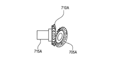
図7に示されるように、他の実施形態では、試料102または円筒柱形試料502は、歯車710を介してアーム715に回転可能に連結されたマニピュレータ705に取り付けることができ、アーム715は、TEM試料チャンバの側面600に直角に入る。アーム715がその回転軸720の周りで連続して120度の角度ずつ回転されると、歯車715は、軸720から、図示のように試料(または関心領域)102の対蹠的な頂点を通過するマニピュレータ705の回転軸120に、回転運動を伝達する。したがって、歯車710は、アーム715の連続的な120度の回転を試料(または関心領域)102の回転軸120の周りでの連続的な120度の回転に変換して、試料(または関心領域)102の3つの直交面を電子ビーム101にさらし、それにより、TEMが試料(または関心領域)102の3つの直交画像を取得することを可能にする。
As shown in FIG. 7, in other embodiments, the
図8Aおよび8Bは、第1の軸から第2の軸へ回転運動を伝達するために使用することができるちょうど2つのタイプの歯車の概略図である。当業者であれば、他のそのような機構を特定することができるであろう。図8Aに示されるように、回転運動をアーム715/715Aから試料(または関心領域)102が取り付けられるマニピュレータ705/705Aに伝達するために、斜交かさ歯車710Aが使用することができる。あるいは、図8Bに示されるように、回転運動をアーム715/715Bから試料(または関心領域)102が取り付けられるマニピュレータ705/705Bに伝達するために、ねじ歯車710Bが使用することができる。
FIGS. 8A and 8B are schematic views of just two types of gears that can be used to transmit rotational motion from a first axis to a second axis. Those skilled in the art will be able to identify other such mechanisms. As shown in FIG. 8A, an
本発明のいくつかの実施形態によれば、荷電粒子ビーム装置において試料の直交画像を得るための方法が、複数の直交面を有する試料を回転試料ホルダに連結することと、複数の角度のそれぞれにつき試料の複数の直交面のうちの異なる1つの直交面が荷電粒子ビーム装置によって生成された電子ビームにさらされかつ電子ビームに対して垂直になるように、回転試料ホルダを複数の角度に回転させることと、複数の角度のそれぞれにおいて、試料の複数の直交面を透過した電子ビームからの電子を検出することと、複数の角度のそれぞれにおいて検出された試料を透過した電子から試料の複数の画像を生成することと、を含む。 According to some embodiments of the present invention, a method for obtaining an orthogonal image of a sample in a charged particle beam device includes connecting a sample having a plurality of orthogonal surfaces to a rotating sample holder and each of a plurality of angles. Rotate the rotating sample holder at multiple angles so that one of the multiple orthogonal surfaces of the sample is exposed to and perpendicular to the electron beam generated by the charged particle beam device Detecting electrons from an electron beam transmitted through a plurality of orthogonal planes of the sample at each of a plurality of angles, and detecting a plurality of samples from the electrons transmitted through the sample detected at each of a plurality of angles. Generating an image.
いくつかの実施形態では、回転試料ホルダを複数の角度に回転させることは、ゼロ度、+/−120度、および240度からなる群から選択された少なくとも2つの角度に回転試料ホルダを回転させることを含む。いくつかの実施形態では、複数の直交面を有する試料を回転試料ホルダに連結することは、複数の直交面を有する立方体関心領域を含む円筒柱を、円筒柱の軸が立方体関心領域の対蹠的な頂点を通過するように、回転試料ホルダに連結することを含む。いくつかの実施形態では、円筒柱を回転試料ホルダに連結することは、円筒柱を回転試料ホルダに溶接することを含む。 In some embodiments, rotating the rotating sample holder to multiple angles rotates the rotating sample holder to at least two angles selected from the group consisting of zero degrees, +/− 120 degrees, and 240 degrees. Including that. In some embodiments, coupling a sample having a plurality of orthogonal planes to a rotating sample holder may comprise a cylindrical column including a cubic region of interest having a plurality of orthogonal planes, with the axis of the cylindrical column opposite the cubic region of interest. Coupling to a rotating sample holder so as to pass through a general apex. In some embodiments, coupling the cylindrical column to the rotating sample holder includes welding the cylindrical column to the rotating sample holder.
いくつかの実施形態では、複数の直交面を有する試料を回転試料ホルダに連結することは、針の軸が立方体試料の対蹠的な頂点を通過するように立方体試料を針に取り付けることと、その針を回転試料ホルダに連結することとを含む。いくつかの実施形態では、針を回転試料ホルダに連結することは、針を回転試料ホルダに溶接することを含む。いくつかの実施形態では、立方体試料を針に取り付けることは、荷電粒子ビーム装置において環状集束イオン・ビーム・ミリングにより針を作ることと、荷電粒子ビーム装置において集束イオン・ビームを使用してより大きい試料から立方体試料を作ることと、針の軸が立方体試料の対蹠的な頂点を通過するように針を立方体試料に溶接することと、針に取り付けられた立方体試料をより大きい試料から分離することと、をさらに含む。 In some embodiments, coupling a sample having a plurality of orthogonal faces to the rotating sample holder includes attaching the cubic sample to the needle such that the axis of the needle passes through the opposing vertex of the cubic sample; Connecting the needle to a rotating sample holder. In some embodiments, coupling the needle to the rotating sample holder includes welding the needle to the rotating sample holder. In some embodiments, attaching the cubic sample to the needle is larger than making the needle by annular focused ion beam milling in a charged particle beam device and using a focused ion beam in a charged particle beam device. Making a cube sample from the sample, welding the needle to the cube sample so that the axis of the needle passes the opposite vertex of the cube sample, and separating the cube sample attached to the needle from the larger sample And further.
いくつかの実施形態では、回転試料ホルダは、荷電粒子ビーム装置内の壁を斜めの角度で通過する。いくつかの実施形態では、回転試料ホルダは、歯車を介して斜めの角度で回転アームに連結され、また、回転アームは、荷電粒子ビーム装置内の壁を直角に通過する。いくつかの実施形態では、回転試料ホルダを複数の角度に回転させることは、回転アームの複数の角度への回転が歯車により回転試料ホルダの複数の角度への回転に伝達されるように回転アームを複数の角度に回転させることを含む。いくつかの実施形態では、歯車は、斜交かさ歯車またはねじ歯車のうちの少なくとも1つである。 In some embodiments, the rotating sample holder passes through the wall in the charged particle beam device at an oblique angle. In some embodiments, the rotating sample holder is coupled to the rotating arm at an oblique angle via gears, and the rotating arm passes perpendicularly through the wall in the charged particle beam device. In some embodiments, rotating the rotating sample holder to multiple angles means rotating the rotating arm to multiple angles such that rotation of the rotating arm to the multiple angles of the rotating sample holder is transmitted by a gear. Rotating at a plurality of angles. In some embodiments, the gear is at least one of an oblique bevel gear or a screw gear.
本発明のいくつかの実施形態によれば、透過電子顕微鏡において電子ビームを使用して複数の方向で試料を観察するための試料および試料保持装置が、互いに平行でない少なくとも3つの観察面を有する試料であって、観察面のそれぞれに直交する厚さが200nm未満である試料と、試料が取り付けられる針であって、2つ以上の軸の周りで回転可能であり、そのため観察面のうちの少なくとも3つの観察面を電子顕微鏡の電子ビームに対して垂直に配向することができる針と、を備える。 According to some embodiments of the present invention, a sample for observing a sample in a plurality of directions using an electron beam in a transmission electron microscope and a sample holding apparatus having at least three observation surfaces that are not parallel to each other A sample having a thickness of less than 200 nm perpendicular to each of the observation surfaces and a needle to which the sample is attached, and is rotatable about two or more axes, so that at least one of the observation surfaces A needle capable of orienting three observation planes perpendicular to an electron beam of an electron microscope.
本発明のいくつかの実施形態によれば、荷電粒子ビーム装置が、試料の一部分を照射するための荷電粒子ビーム源と、試料の照射部分から放出された放射を検出するための少なくとも1つの検出器と、試料を保持するための試料ホルダであって、試料を取り付けるための針を含み、針が2つ以上の軸の周りで回転可能であり、そのため針が観察面のうちの少なくとも3つが電子顕微鏡の電子ビームに対して垂直になるように試料を配向することができる試料ホルダと、を備える。 According to some embodiments of the present invention, a charged particle beam device includes a charged particle beam source for irradiating a portion of the sample and at least one detection for detecting radiation emitted from the irradiated portion of the sample. And a sample holder for holding the sample, comprising a needle for attaching the sample, the needle being rotatable about two or more axes, so that at least three of the viewing surfaces of the needle are A sample holder capable of orienting the sample so as to be perpendicular to the electron beam of the electron microscope.
いくつかの実施形態では、回転試料ホルダは、ゼロ度、+/−120度、および240度からなる群から選択された少なくとも2つの角度に回転可能である。いくつかの実施形態では、試料は、回転試料ホルダに溶接される。いくつかの実施形態では、針は、回転試料ホルダに溶接される。いくつかの実施形態では、回転試料ホルダは、荷電粒子ビーム装置内の壁を斜めの角度で通過する。 In some embodiments, the rotating sample holder is rotatable to at least two angles selected from the group consisting of zero degrees, +/− 120 degrees, and 240 degrees. In some embodiments, the sample is welded to the rotating sample holder. In some embodiments, the needle is welded to the rotating sample holder. In some embodiments, the rotating sample holder passes through the wall in the charged particle beam device at an oblique angle.
いくつかの実施形態では、回転試料ホルダは、歯車を介して斜めの角度で回転アームに連結され、また、回転アームは、荷電粒子ビーム装置内の壁を直角に通過する。いくつかの実施形態では、回転アームの複数の角度への回転は、歯車により回転試料ホルダの複数の角度への回転に伝達される。いくつかの実施形態では、歯車は、斜交かさ歯車またはねじ歯車のうちの少なくとも1つである。 In some embodiments, the rotating sample holder is coupled to the rotating arm at an oblique angle via gears, and the rotating arm passes perpendicularly through the wall in the charged particle beam device. In some embodiments, rotation of the rotating arm to multiple angles is transmitted by gears to rotation of the rotating sample holder to multiple angles. In some embodiments, the gear is at least one of an oblique bevel gear or a screw gear.
以上の説明の多くは、ICデバイスの特徴および構成部品を対象としているが、本発明は、任意の適切な材料のバルク試料を視覚化するために使用することができる。「被加工物」、「試料」、「基板」、および「試験体」という用語は、特記しない限り、本出願においては相互に交換可能に使用されている。さらに、本明細書において、用語「自動」、「自動化された」または類似の用語が使用されるとき、これらの用語は、自動プロセスもしくは自動ステップまたは自動化されたプロセスもしくは自動化されたステップの手動による開始を含むものと理解されるであろう。 Although much of the above description is directed to IC device features and components, the present invention can be used to visualize bulk samples of any suitable material. Unless otherwise stated, the terms “workpiece”, “sample”, “substrate”, and “specimen” are used interchangeably in this application. Furthermore, when the terms “automatic”, “automated” or similar terms are used herein, these terms are either automated processes or automated steps or automated processes or automated steps manually. It will be understood to include initiation.
論述および特許請求の範囲において、「含む(including)」および「備える(comprising)」という用語は、オープン・エンド様式で使用されており、「〜を含むがそれに限定されない」ことを意味するものと解釈されるべきである。いかなる用語も、本明細書において特に定義されていない限り、その用語は、その一般的かつ通常の意味が与えられることが意図されている。添付の図面は、本発明の理解を助けることが意図されており、特に指示のない限り、一定の比例に応じては描かれていない。本発明を実施するのに適した粒子ビーム・システムは、例えば、本出願の譲受人であるFEI Companyから市販されている。 In the discussion and in the claims, the terms “including” and “comprising” are used in an open-ended manner and shall mean “including but not limited to” Should be interpreted. Unless any term is specifically defined herein, the term is intended to be given its general and ordinary meaning. The accompanying drawings are intended to assist in understanding the present invention and are not drawn to scale unless otherwise indicated. Suitable particle beam systems for practicing the present invention are commercially available, for example, from the FEI Company, the assignee of the present application.
本発明および本発明の利点を詳細に説明したが、添付の特許請求項の範囲によって定義された本発明の精神および範囲から逸脱することなく、本明細書に記載の実施形態に様々な変更、置換、および改変がなされ得ることが、理解されるべきである。さらに、本出願の範囲は、本明細書に記載の特定の実施形態に限定されるものではない。当業者であれば本開示から容易に理解するであろうように、本明細書に記載の対応する実施形態と実質的に同じ機能を実行するかまたは実質的に同じ結果を達成する既存のまたは今後開発されるプロセス、機械、製造、組成物、手段、方法、もしくはステップが、本発明に従って利用され得る。したがって、添付の特許請求の範囲は、そのようなプロセス、機械、製造、組成物、手段、方法、またはステップをその範囲に含むことが意図されている。 Having described the invention and its advantages in detail, various modifications may be made to the embodiments described herein without departing from the spirit and scope of the invention as defined by the appended claims. It should be understood that substitutions and modifications can be made. Further, the scope of the present application is not limited to the specific embodiments described herein. As one of ordinary skill in the art will readily appreciate from the present disclosure, an existing or performing substantially the same function or achieving substantially the same result as the corresponding embodiments described herein. Future developed processes, machines, manufacture, compositions, means, methods, or steps may be utilized in accordance with the present invention. Accordingly, the appended claims are intended to include within their scope such processes, machines, manufacture, compositions of matter, means, methods, or steps.
101 電子ビーム
102 試料
105 針
110 薄片
115 断層撮影ピン・ホルダ
101
Claims (14)
互いに平行でない3つの直交面を有する試料を回転試料ホルダに連結することと、
複数の角度のそれぞれにつき前記3つの直交面のうちの異なる1つの直交面が前記荷電粒子ビーム装置によって生成された電子ビームにさらされかつ前記電子ビームに対して垂直になるように、前記回転試料ホルダを前記複数の角度に回転させることと、
前記複数の角度のそれぞれにおいて、前記3つの直交面のそれぞれを透過した前記電子ビームからの前記電子を検出することと、
前記3つの直交面のそれぞれにおいて前記試料を透過した前記検出された電子から前記試料の3つの直交する画像を生成することと
を含み、
前記試料は立方体試料であり、
前記立方体試料は、針の軸が前記立方体試料の対蹠的な頂点を通過するように前記回転試料ホルダに連結された針に取り付けられる、方法。 A method for obtaining an orthogonal image of a sample in a charged particle beam device, comprising:
Connecting a sample having three orthogonal surfaces that are not parallel to each other to a rotating sample holder;
The rotating sample so that a different one of the three orthogonal surfaces for each of a plurality of angles is exposed to and perpendicular to the electron beam generated by the charged particle beam device. Rotating the holder to the plurality of angles;
Detecting the electrons from the electron beam transmitted through each of the three orthogonal surfaces at each of the plurality of angles;
See containing and generating the three orthogonal images of the sample from said detected electrons transmitted through the sample in each of the three orthogonal planes,
The sample is a cubic sample;
The cube sample is attached to a needle connected to the rotating sample holder such that the axis of the needle passes through the opposite apex of the cube sample .
針の軸が立方体試料の対蹠的な頂点を通過するように前記立方体試料を前記針に取り付けることと、前記針を回転試料ホルダに連結することとによって、互いに平行でない3つの直交面を有する前記立方体試料を前記回転試料ホルダに連結することと、
複数の角度のそれぞれにつき前記3つの直交面のうちの異なる1つの直交面が前記荷電粒子ビーム装置によって生成された電子ビームにさらされかつ前記電子ビームに対して垂直になるように、前記回転試料ホルダを前記複数の角度に回転させることと、
前記複数の角度のそれぞれにおいて、前記3つの直交面のそれぞれを透過した前記電子ビームからの前記電子を検出することと、
前記3つの直交面のそれぞれにおいて前記立方体試料を透過した前記検出された電子から前記立方体試料の3つの直交する画像を生成することと
を含み、
前記立方体試料を前記針に取り付けることが、
前記荷電粒子ビーム装置において環状集束イオン・ビーム・ミリングにより前記針を作ることと、
前記荷電粒子ビーム装置において集束イオン・ビームを使用してより大きい試料から前記立方体試料を作ることと、
前記針の軸が前記立方体試料の対蹠的な頂点を通過するように、前記針を前記立方体試料に溶接することと、
前記針に取り付けられた前記立方体試料を前記より大きい試料から分離することと
をさらに含む、方法。 A method for obtaining an orthogonal image of a sample in a charged particle beam device, comprising:
By attaching the cube sample to the needle so that the axis of the needle passes through the opposite vertex of the cube sample and connecting the needle to a rotating sample holder, it has three orthogonal planes that are not parallel to each other Connecting the cube sample to the rotating sample holder;
The rotating sample so that a different one of the three orthogonal surfaces for each of a plurality of angles is exposed to and perpendicular to the electron beam generated by the charged particle beam device. Rotating the holder to the plurality of angles;
Detecting the electrons from the electron beam transmitted through each of the three orthogonal surfaces at each of the plurality of angles;
Generating three orthogonal images of the cubic sample from the detected electrons transmitted through the cubic sample in each of the three orthogonal planes;
Including
Attaching the cubic sample to the needle;
Making the needle by annular focused ion beam milling in the charged particle beam device;
Creating the cubic sample from a larger sample using a focused ion beam in the charged particle beam device;
Welding the needle to the cube sample such that the axis of the needle passes through the opposite apex of the cube sample;
Further comprising, a method and separating said cubes sample attached to the needle from the larger sample.
互いに平行でない3つの直交面を有する試料を回転試料ホルダに連結することと、
複数の角度のそれぞれにつき前記3つの直交面のうちの異なる1つの直交面が前記荷電粒子ビーム装置によって生成された電子ビームにさらされかつ前記電子ビームに対して垂直になるように、前記回転試料ホルダを前記複数の角度に回転させることと、
前記複数の角度のそれぞれにおいて、前記3つの直交面のそれぞれを透過した前記電子ビームからの前記電子を検出することと、
前記3つの直交面のそれぞれにおいて前記試料を透過した前記検出された電子から前記試料の3つの直交する画像を生成することと
を含み、
前記回転試料ホルダが、前記荷電粒子ビーム装置内の壁を斜めの角度で通過する、方法。 A method for obtaining an orthogonal image of a sample in a charged particle beam device, comprising:
Connecting a sample having three orthogonal surfaces that are not parallel to each other to a rotating sample holder;
The rotating sample so that a different one of the three orthogonal surfaces for each of a plurality of angles is exposed to and perpendicular to the electron beam generated by the charged particle beam device. Rotating the holder to the plurality of angles;
Detecting the electrons from the electron beam transmitted through each of the three orthogonal surfaces at each of the plurality of angles;
Generating three orthogonal images of the sample from the detected electrons transmitted through the sample in each of the three orthogonal planes;
Including
The rotating sample holder passes through the wall of said charged particle beam device at an oblique angle, the method.
互いに平行でない少なくとも3つの観察面を有する立方体試料であって、前記観察面のそれぞれに直交する厚さが200nm未満である立方体試料と、
前記立方体試料が取り付けられる針であって、前記針の軸が前記立方体試料の対蹠的な頂点を通過するように取り付けられ、2つ以上の軸の周りで回転可能であり、そのため前記観察面のうちの少なくとも3つの観察面を透過電子顕微鏡の電子ビームに対して垂直に配向することができる針を含む試料保持装置と
を備える、試料アセンブリ。 A sample assembly for a transmission electron microscope that performs multi-directional observation using an electron beam,
A cubic sample having at least three viewing surface not parallel to each other, the cubic sample thickness orthogonal to each of the observation plane is less than 200 nm,
A needle to which the cube sample is attached, wherein the axis of the needle is attached so that it passes through opposite vertices of the cube sample and is rotatable about two or more axes, so that the viewing surface A sample holder comprising a needle capable of orienting at least three of the viewing planes perpendicular to the electron beam of a transmission electron microscope.
前記試料を保持するための試料ホルダであって、前記試料ホルダは前記試料を取り付けるための針を含み、前記針が、2つ以上の軸の周りで回転可能であり、前記試料を前記針に取り付けている間に、少なくとも3つの観察面のそれぞれを前記電子顕微鏡の前記電子ビームに対して垂直に配向することができる試料ホルダと、
前記電子ビームが、前記少なくとも3つの観察面のうちの1つの観察面に対して垂直な前記試料のそれぞれの配向において、前記試料を透過し前記試料から放出された前記電子ビームの電子を検出するよう構成された少なくとも1つの検出器と
を備え、
前記試料ホルダが、前記荷電粒子ビーム装置内の壁を斜めの角度で通過する、荷電粒子ビーム装置。 An electron microscope comprising an electron beam source for transmitting the electron beam through a sample having at least three observation surfaces that are not parallel to each other;
A sample holder for holding the sample, wherein the sample holder includes a needle for attaching the sample, the needle is rotatable about two or more axes, and the sample is attached to the needle. A sample holder capable of orienting each of at least three viewing planes perpendicular to the electron beam of the electron microscope during mounting;
The electron beam detects electrons of the electron beam transmitted through the sample and emitted from the sample in each orientation of the sample perpendicular to one of the at least three observation surfaces. and at least one detector configured,
The sample holder, it passes through the wall of said charged particle beam device at an oblique angle, the charged particle beam device.
前記針が、前記回転可能な軸に溶接され、前記回転可能な軸の回転が前記針を回転させる、請求項10に記載の荷電粒子ビーム装置。 The sample holder includes a rotatable shaft;
The charged particle beam device according to claim 10 , wherein the needle is welded to the rotatable shaft, and rotation of the rotatable shaft rotates the needle.
集束イオン・ビームを用いて、より大きい材料片から関心領域を含む試料を抽出することであって、抽出された前記試料は3つの直交面を有し、前記直交面のそれぞれを透過する電子に対して部分的に透過性であることと、 Using a focused ion beam to extract a sample containing a region of interest from a larger piece of material, the extracted sample having three orthogonal planes, and electrons passing through each of the orthogonal planes. Partly transparent to it,
抽出された前記試料を細い針に取り付けることと、 Attaching the extracted sample to a thin needle;
電子ビームに第1の直交面を透過させることによって前記試料の第1の画像を得ることと、 Obtaining a first image of the sample by transmitting an electron beam through a first orthogonal plane;
前記電子ビームに第2の直交面をさらすために前記試料を回転することと、 Rotating the sample to expose a second orthogonal plane to the electron beam;
前記電子ビームに前記第2の直交面を透過させることによって前記試料の第2の画像を得ることと、 Obtaining a second image of the sample by transmitting the electron beam through the second orthogonal plane;
前記電子ビームに第3の直交面を曝すために前記試料を回転することと、 Rotating the sample to expose a third orthogonal plane to the electron beam;
前記電子ビームに前記第3の直交面を透過させることによって前記試料の第3の画像を得ることと、 Obtaining a third image of the sample by transmitting the electron beam through the third orthogonal plane;
前記第1、第2および第3の画像を用いて断層撮影再構成を実行することなく、前記第1、第2および第3の画像を観察することと、 Observing the first, second and third images without performing tomographic reconstruction using the first, second and third images;
を含む、方法。 Including a method.
Applications Claiming Priority (2)
| Application Number | Priority Date | Filing Date | Title |
|---|---|---|---|
| US201462027035P | 2014-07-21 | 2014-07-21 | |
| US62/027,035 | 2014-07-21 |
Publications (3)
| Publication Number | Publication Date |
|---|---|
| JP2016025085A JP2016025085A (en) | 2016-02-08 |
| JP2016025085A5 JP2016025085A5 (en) | 2017-11-24 |
| JP6385899B2 true JP6385899B2 (en) | 2018-09-05 |
Family
ID=55075144
Family Applications (1)
| Application Number | Title | Priority Date | Filing Date |
|---|---|---|---|
| JP2015142246A Expired - Fee Related JP6385899B2 (en) | 2014-07-21 | 2015-07-16 | TEM sample mounting structure |
Country Status (3)
| Country | Link |
|---|---|
| US (1) | US9514913B2 (en) |
| JP (1) | JP6385899B2 (en) |
| CN (1) | CN105277576B (en) |
Families Citing this family (5)
| Publication number | Priority date | Publication date | Assignee | Title |
|---|---|---|---|---|
| DE102015215323A1 (en) * | 2015-08-11 | 2017-02-16 | Georg-August-Universität Göttingen Stiftung Öffentlichen Rechts | Technique for tomographic image acquisition |
| CN110118791B (en) * | 2019-05-21 | 2020-03-03 | 山东省分析测试中心 | EBSD equipment sample stage and method for acquiring crack/grain boundary three-dimensional information |
| CN110672881A (en) * | 2019-09-30 | 2020-01-10 | 上海华力集成电路制造有限公司 | Metal gate structure and method of fabricating the same |
| CN113063967B (en) * | 2021-02-18 | 2023-02-10 | 上海大学 | Rotary sample table device capable of realizing three-dimensional atom probe microtip array sample rotation |
| CN115047016A (en) * | 2022-08-16 | 2022-09-13 | 合肥晶合集成电路股份有限公司 | Three-dimensional TEM sample structure and preparation method thereof |
Family Cites Families (18)
| Publication number | Priority date | Publication date | Assignee | Title |
|---|---|---|---|---|
| JPS62281349A (en) | 1986-05-29 | 1987-12-07 | Seiko Instr & Electronics Ltd | Formation of metallic pattern film and apparatus therefor |
| US5104684A (en) | 1990-05-25 | 1992-04-14 | Massachusetts Institute Of Technology | Ion beam induced deposition of metals |
| BE1007675A3 (en) | 1993-10-28 | 1995-09-12 | Philips Electronics Nv | Process for the production of preparations intended for an electron microscope. |
| JPH08304243A (en) * | 1995-05-11 | 1996-11-22 | Nippon Steel Corp | Sample having cross sectional thin-film, its manufacture, and its holder |
| US7297965B2 (en) | 2004-07-14 | 2007-11-20 | Applied Materials, Israel, Ltd. | Method and apparatus for sample formation and microanalysis in a vacuum chamber |
| US7442924B2 (en) | 2005-02-23 | 2008-10-28 | Fei, Company | Repetitive circumferential milling for sample preparation |
| JP4851804B2 (en) | 2006-02-13 | 2012-01-11 | 株式会社日立ハイテクノロジーズ | Focused ion beam processing observation apparatus, focused ion beam processing observation system, and processing observation method |
| JP4923716B2 (en) * | 2006-05-11 | 2012-04-25 | 株式会社日立製作所 | Sample analysis apparatus and sample analysis method |
| EP1890136A1 (en) | 2006-08-16 | 2008-02-20 | FEI Company | Method for obtaining images from slices of a specimen |
| CN200982932Y (en) * | 2006-11-03 | 2007-11-28 | 中国科学院金属研究所 | A device for using ion beam sample processing interface to realize bear dispersion |
| US7884326B2 (en) | 2007-01-22 | 2011-02-08 | Fei Company | Manipulator for rotating and translating a sample holder |
| EP2051280A1 (en) | 2007-10-18 | 2009-04-22 | The Regents of the University of California | Motorized manipulator for positioning a TEM specimen |
| JP5268324B2 (en) * | 2007-10-29 | 2013-08-21 | 株式会社日立ハイテクノロジーズ | Charged particle beam microscope and microscope method |
| JP2009192341A (en) | 2008-02-14 | 2009-08-27 | Sumitomo Metal Mining Co Ltd | Preparation method of sliced sample for transmission electron microscope, and sample stand used therefor |
| TWI372859B (en) | 2008-10-03 | 2012-09-21 | Inotera Memories Inc | Method for manufacturing an electron tomography specimen with fiducial markers and method for constructing 3d image |
| JP5883658B2 (en) * | 2012-01-20 | 2016-03-15 | 株式会社日立ハイテクノロジーズ | Charged particle beam microscope, charged particle beam microscope sample holder, and charged particle beam microscope method |
| US8502172B1 (en) | 2012-06-26 | 2013-08-06 | Fei Company | Three dimensional fiducial |
| WO2014195998A1 (en) * | 2013-06-03 | 2014-12-11 | 株式会社日立製作所 | Charged particle microscope, sample holder for charged particle microscope and charged particle microscopy method |
-
2015
- 2015-07-16 JP JP2015142246A patent/JP6385899B2/en not_active Expired - Fee Related
- 2015-07-17 US US14/802,119 patent/US9514913B2/en active Active
- 2015-07-20 CN CN201510551041.4A patent/CN105277576B/en not_active Expired - Fee Related
Also Published As
| Publication number | Publication date |
|---|---|
| CN105277576A (en) | 2016-01-27 |
| JP2016025085A (en) | 2016-02-08 |
| CN105277576B (en) | 2019-08-27 |
| US9514913B2 (en) | 2016-12-06 |
| US20160020065A1 (en) | 2016-01-21 |
Similar Documents
| Publication | Publication Date | Title |
|---|---|---|
| JP6385899B2 (en) | TEM sample mounting structure | |
| US8476588B2 (en) | Method of electron diffraction tomography | |
| JP6700664B2 (en) | Fabrication of malleable slices for correlated atomic resolution tomography analysis | |
| JP3287858B2 (en) | Electron microscope device and electron microscope method | |
| WO2010125754A1 (en) | Composite charged particle radiation device | |
| CN105388173A (en) | Method of acquiring ebsp patterns | |
| US9659743B2 (en) | Image creating method and imaging system for performing the same | |
| JP2016156812A (en) | Pattern matching using lamella of known shape for automated s/tem acquisition and measurement | |
| JP6393448B2 (en) | Reference mark formation for acquisition and alignment of TEM / STEM tomography continuous tilt | |
| JP2012048819A (en) | Charged particle beam device and sample observation method | |
| US9857318B2 (en) | Method for generating image data relating to an object and particle beam device for carrying out this method | |
| US8901510B2 (en) | Particle beam device having a detector arrangement | |
| KR102144555B1 (en) | Method and system for reducing curtaining in charged particle beam sample preparation | |
| KR102169574B1 (en) | Charged particle beam apparatus | |
| Ritter et al. | A practical approach to test the scope of FIB-SEM 3D reconstruction | |
| Roussel et al. | Extreme high resolution scanning electron microscopy (XHR SEM) and beyond | |
| JP4433092B2 (en) | Three-dimensional structure observation method | |
| EP3125270B1 (en) | Tem sample mounting geometry | |
| US20220157560A1 (en) | Method and device for preparing a microscopic sample from a volume sample | |
| WO2019016855A1 (en) | Method for setting inspection conditions for x-ray inspection apparatus | |
| JP2022509915A (en) | Electron diffraction imaging system for determining molecular structure and conformation | |
| Lee et al. | Detection of micro defects in 3dic packages by means of non-destructive 3D X-ray | |
| Hrnčíř et al. | Variable Angle TEM Grid Holder for Advanced TEM Lamellae Preparation | |
| Wang et al. | X-ray microscopy for NDE of micro-and nano-structrues | |
| JP2023076412A (en) | Method of imaging and milling sample |
Legal Events
| Date | Code | Title | Description |
|---|---|---|---|
| A521 | Request for written amendment filed |
Free format text: JAPANESE INTERMEDIATE CODE: A523 Effective date: 20171015 |
|
| A621 | Written request for application examination |
Free format text: JAPANESE INTERMEDIATE CODE: A621 Effective date: 20171015 |
|
| A871 | Explanation of circumstances concerning accelerated examination |
Free format text: JAPANESE INTERMEDIATE CODE: A871 Effective date: 20171016 |
|
| A977 | Report on retrieval |
Free format text: JAPANESE INTERMEDIATE CODE: A971007 Effective date: 20180112 |
|
| A975 | Report on accelerated examination |
Free format text: JAPANESE INTERMEDIATE CODE: A971005 Effective date: 20180116 |
|
| A131 | Notification of reasons for refusal |
Free format text: JAPANESE INTERMEDIATE CODE: A131 Effective date: 20180123 |
|
| A601 | Written request for extension of time |
Free format text: JAPANESE INTERMEDIATE CODE: A601 Effective date: 20180422 |
|
| A601 | Written request for extension of time |
Free format text: JAPANESE INTERMEDIATE CODE: A601 Effective date: 20180622 |
|
| A521 | Request for written amendment filed |
Free format text: JAPANESE INTERMEDIATE CODE: A523 Effective date: 20180715 |
|
| TRDD | Decision of grant or rejection written | ||
| A01 | Written decision to grant a patent or to grant a registration (utility model) |
Free format text: JAPANESE INTERMEDIATE CODE: A01 Effective date: 20180724 |
|
| A61 | First payment of annual fees (during grant procedure) |
Free format text: JAPANESE INTERMEDIATE CODE: A61 Effective date: 20180808 |
|
| R150 | Certificate of patent or registration of utility model |
Ref document number: 6385899 Country of ref document: JP Free format text: JAPANESE INTERMEDIATE CODE: R150 |
|
| R250 | Receipt of annual fees |
Free format text: JAPANESE INTERMEDIATE CODE: R250 |
|
| LAPS | Cancellation because of no payment of annual fees |