JP6385234B2 - Semiconductor device - Google Patents
Semiconductor device Download PDFInfo
- Publication number
- JP6385234B2 JP6385234B2 JP2014211424A JP2014211424A JP6385234B2 JP 6385234 B2 JP6385234 B2 JP 6385234B2 JP 2014211424 A JP2014211424 A JP 2014211424A JP 2014211424 A JP2014211424 A JP 2014211424A JP 6385234 B2 JP6385234 B2 JP 6385234B2
- Authority
- JP
- Japan
- Prior art keywords
- lead terminal
- semiconductor element
- semiconductor device
- sealing resin
- bonded
- Prior art date
- Legal status (The legal status is an assumption and is not a legal conclusion. Google has not performed a legal analysis and makes no representation as to the accuracy of the status listed.)
- Active
Links
Images


Classifications
-
- H—ELECTRICITY
- H01—ELECTRIC ELEMENTS
- H01L—SEMICONDUCTOR DEVICES NOT COVERED BY CLASS H10
- H01L23/00—Details of semiconductor or other solid state devices
- H01L23/28—Encapsulations, e.g. encapsulating layers, coatings, e.g. for protection
- H01L23/29—Encapsulations, e.g. encapsulating layers, coatings, e.g. for protection characterised by the material, e.g. carbon
-
- H—ELECTRICITY
- H01—ELECTRIC ELEMENTS
- H01L—SEMICONDUCTOR DEVICES NOT COVERED BY CLASS H10
- H01L24/00—Arrangements for connecting or disconnecting semiconductor or solid-state bodies; Methods or apparatus related thereto
- H01L24/01—Means for bonding being attached to, or being formed on, the surface to be connected, e.g. chip-to-package, die-attach, "first-level" interconnects; Manufacturing methods related thereto
- H01L24/42—Wire connectors; Manufacturing methods related thereto
- H01L24/47—Structure, shape, material or disposition of the wire connectors after the connecting process
-
- H—ELECTRICITY
- H01—ELECTRIC ELEMENTS
- H01L—SEMICONDUCTOR DEVICES NOT COVERED BY CLASS H10
- H01L23/00—Details of semiconductor or other solid state devices
- H01L23/562—Protection against mechanical damage
-
- H—ELECTRICITY
- H01—ELECTRIC ELEMENTS
- H01L—SEMICONDUCTOR DEVICES NOT COVERED BY CLASS H10
- H01L23/00—Details of semiconductor or other solid state devices
-
- H—ELECTRICITY
- H01—ELECTRIC ELEMENTS
- H01L—SEMICONDUCTOR DEVICES NOT COVERED BY CLASS H10
- H01L23/00—Details of semiconductor or other solid state devices
- H01L23/28—Encapsulations, e.g. encapsulating layers, coatings, e.g. for protection
- H01L23/29—Encapsulations, e.g. encapsulating layers, coatings, e.g. for protection characterised by the material, e.g. carbon
- H01L23/293—Organic, e.g. plastic
-
- H—ELECTRICITY
- H01—ELECTRIC ELEMENTS
- H01L—SEMICONDUCTOR DEVICES NOT COVERED BY CLASS H10
- H01L23/00—Details of semiconductor or other solid state devices
- H01L23/28—Encapsulations, e.g. encapsulating layers, coatings, e.g. for protection
- H01L23/31—Encapsulations, e.g. encapsulating layers, coatings, e.g. for protection characterised by the arrangement or shape
- H01L23/3107—Encapsulations, e.g. encapsulating layers, coatings, e.g. for protection characterised by the arrangement or shape the device being completely enclosed
- H01L23/3121—Encapsulations, e.g. encapsulating layers, coatings, e.g. for protection characterised by the arrangement or shape the device being completely enclosed a substrate forming part of the encapsulation
-
- H—ELECTRICITY
- H01—ELECTRIC ELEMENTS
- H01L—SEMICONDUCTOR DEVICES NOT COVERED BY CLASS H10
- H01L23/00—Details of semiconductor or other solid state devices
- H01L23/28—Encapsulations, e.g. encapsulating layers, coatings, e.g. for protection
- H01L23/31—Encapsulations, e.g. encapsulating layers, coatings, e.g. for protection characterised by the arrangement or shape
- H01L23/3107—Encapsulations, e.g. encapsulating layers, coatings, e.g. for protection characterised by the arrangement or shape the device being completely enclosed
- H01L23/3135—Double encapsulation or coating and encapsulation
-
- H—ELECTRICITY
- H01—ELECTRIC ELEMENTS
- H01L—SEMICONDUCTOR DEVICES NOT COVERED BY CLASS H10
- H01L23/00—Details of semiconductor or other solid state devices
- H01L23/28—Encapsulations, e.g. encapsulating layers, coatings, e.g. for protection
- H01L23/31—Encapsulations, e.g. encapsulating layers, coatings, e.g. for protection characterised by the arrangement or shape
- H01L23/3157—Partial encapsulation or coating
- H01L23/3185—Partial encapsulation or coating the coating covering also the sidewalls of the semiconductor body
-
- H—ELECTRICITY
- H01—ELECTRIC ELEMENTS
- H01L—SEMICONDUCTOR DEVICES NOT COVERED BY CLASS H10
- H01L23/00—Details of semiconductor or other solid state devices
- H01L23/48—Arrangements for conducting electric current to or from the solid state body in operation, e.g. leads, terminal arrangements ; Selection of materials therefor
- H01L23/488—Arrangements for conducting electric current to or from the solid state body in operation, e.g. leads, terminal arrangements ; Selection of materials therefor consisting of soldered or bonded constructions
- H01L23/495—Lead-frames or other flat leads
- H01L23/49517—Additional leads
- H01L23/4952—Additional leads the additional leads being a bump or a wire
-
- H—ELECTRICITY
- H01—ELECTRIC ELEMENTS
- H01L—SEMICONDUCTOR DEVICES NOT COVERED BY CLASS H10
- H01L23/00—Details of semiconductor or other solid state devices
- H01L23/48—Arrangements for conducting electric current to or from the solid state body in operation, e.g. leads, terminal arrangements ; Selection of materials therefor
- H01L23/488—Arrangements for conducting electric current to or from the solid state body in operation, e.g. leads, terminal arrangements ; Selection of materials therefor consisting of soldered or bonded constructions
- H01L23/495—Lead-frames or other flat leads
- H01L23/49541—Geometry of the lead-frame
- H01L23/49548—Cross section geometry
- H01L23/49551—Cross section geometry characterised by bent parts
-
- H—ELECTRICITY
- H01—ELECTRIC ELEMENTS
- H01L—SEMICONDUCTOR DEVICES NOT COVERED BY CLASS H10
- H01L23/00—Details of semiconductor or other solid state devices
- H01L23/48—Arrangements for conducting electric current to or from the solid state body in operation, e.g. leads, terminal arrangements ; Selection of materials therefor
- H01L23/488—Arrangements for conducting electric current to or from the solid state body in operation, e.g. leads, terminal arrangements ; Selection of materials therefor consisting of soldered or bonded constructions
- H01L23/495—Lead-frames or other flat leads
- H01L23/49575—Assemblies of semiconductor devices on lead frames
-
- H—ELECTRICITY
- H01—ELECTRIC ELEMENTS
- H01L—SEMICONDUCTOR DEVICES NOT COVERED BY CLASS H10
- H01L23/00—Details of semiconductor or other solid state devices
- H01L23/48—Arrangements for conducting electric current to or from the solid state body in operation, e.g. leads, terminal arrangements ; Selection of materials therefor
- H01L23/488—Arrangements for conducting electric current to or from the solid state body in operation, e.g. leads, terminal arrangements ; Selection of materials therefor consisting of soldered or bonded constructions
- H01L23/498—Leads, i.e. metallisations or lead-frames on insulating substrates, e.g. chip carriers
- H01L23/49838—Geometry or layout
-
- H—ELECTRICITY
- H01—ELECTRIC ELEMENTS
- H01L—SEMICONDUCTOR DEVICES NOT COVERED BY CLASS H10
- H01L24/00—Arrangements for connecting or disconnecting semiconductor or solid-state bodies; Methods or apparatus related thereto
- H01L24/01—Means for bonding being attached to, or being formed on, the surface to be connected, e.g. chip-to-package, die-attach, "first-level" interconnects; Manufacturing methods related thereto
- H01L24/34—Strap connectors, e.g. copper straps for grounding power devices; Manufacturing methods related thereto
- H01L24/36—Structure, shape, material or disposition of the strap connectors prior to the connecting process
- H01L24/37—Structure, shape, material or disposition of the strap connectors prior to the connecting process of an individual strap connector
-
- H—ELECTRICITY
- H01—ELECTRIC ELEMENTS
- H01L—SEMICONDUCTOR DEVICES NOT COVERED BY CLASS H10
- H01L24/00—Arrangements for connecting or disconnecting semiconductor or solid-state bodies; Methods or apparatus related thereto
- H01L24/01—Means for bonding being attached to, or being formed on, the surface to be connected, e.g. chip-to-package, die-attach, "first-level" interconnects; Manufacturing methods related thereto
- H01L24/34—Strap connectors, e.g. copper straps for grounding power devices; Manufacturing methods related thereto
- H01L24/39—Structure, shape, material or disposition of the strap connectors after the connecting process
- H01L24/40—Structure, shape, material or disposition of the strap connectors after the connecting process of an individual strap connector
-
- H—ELECTRICITY
- H01—ELECTRIC ELEMENTS
- H01L—SEMICONDUCTOR DEVICES NOT COVERED BY CLASS H10
- H01L25/00—Assemblies consisting of a plurality of individual semiconductor or other solid state devices ; Multistep manufacturing processes thereof
- H01L25/03—Assemblies consisting of a plurality of individual semiconductor or other solid state devices ; Multistep manufacturing processes thereof all the devices being of a type provided for in the same subgroup of groups H01L27/00 - H01L33/00, or in a single subclass of H10K, H10N, e.g. assemblies of rectifier diodes
- H01L25/04—Assemblies consisting of a plurality of individual semiconductor or other solid state devices ; Multistep manufacturing processes thereof all the devices being of a type provided for in the same subgroup of groups H01L27/00 - H01L33/00, or in a single subclass of H10K, H10N, e.g. assemblies of rectifier diodes the devices not having separate containers
- H01L25/07—Assemblies consisting of a plurality of individual semiconductor or other solid state devices ; Multistep manufacturing processes thereof all the devices being of a type provided for in the same subgroup of groups H01L27/00 - H01L33/00, or in a single subclass of H10K, H10N, e.g. assemblies of rectifier diodes the devices not having separate containers the devices being of a type provided for in group H01L29/00
- H01L25/072—Assemblies consisting of a plurality of individual semiconductor or other solid state devices ; Multistep manufacturing processes thereof all the devices being of a type provided for in the same subgroup of groups H01L27/00 - H01L33/00, or in a single subclass of H10K, H10N, e.g. assemblies of rectifier diodes the devices not having separate containers the devices being of a type provided for in group H01L29/00 the devices being arranged next to each other
-
- H—ELECTRICITY
- H01—ELECTRIC ELEMENTS
- H01L—SEMICONDUCTOR DEVICES NOT COVERED BY CLASS H10
- H01L25/00—Assemblies consisting of a plurality of individual semiconductor or other solid state devices ; Multistep manufacturing processes thereof
- H01L25/18—Assemblies consisting of a plurality of individual semiconductor or other solid state devices ; Multistep manufacturing processes thereof the devices being of types provided for in two or more different subgroups of the same main group of groups H01L27/00 - H01L33/00, or in a single subclass of H10K, H10N
-
- H—ELECTRICITY
- H01—ELECTRIC ELEMENTS
- H01L—SEMICONDUCTOR DEVICES NOT COVERED BY CLASS H10
- H01L2224/00—Indexing scheme for arrangements for connecting or disconnecting semiconductor or solid-state bodies and methods related thereto as covered by H01L24/00
- H01L2224/01—Means for bonding being attached to, or being formed on, the surface to be connected, e.g. chip-to-package, die-attach, "first-level" interconnects; Manufacturing methods related thereto
- H01L2224/02—Bonding areas; Manufacturing methods related thereto
- H01L2224/04—Structure, shape, material or disposition of the bonding areas prior to the connecting process
- H01L2224/05—Structure, shape, material or disposition of the bonding areas prior to the connecting process of an individual bonding area
- H01L2224/0554—External layer
- H01L2224/0555—Shape
- H01L2224/05552—Shape in top view
- H01L2224/05554—Shape in top view being square
-
- H—ELECTRICITY
- H01—ELECTRIC ELEMENTS
- H01L—SEMICONDUCTOR DEVICES NOT COVERED BY CLASS H10
- H01L2224/00—Indexing scheme for arrangements for connecting or disconnecting semiconductor or solid-state bodies and methods related thereto as covered by H01L24/00
- H01L2224/01—Means for bonding being attached to, or being formed on, the surface to be connected, e.g. chip-to-package, die-attach, "first-level" interconnects; Manufacturing methods related thereto
- H01L2224/02—Bonding areas; Manufacturing methods related thereto
- H01L2224/04—Structure, shape, material or disposition of the bonding areas prior to the connecting process
- H01L2224/06—Structure, shape, material or disposition of the bonding areas prior to the connecting process of a plurality of bonding areas
- H01L2224/0601—Structure
- H01L2224/0603—Bonding areas having different sizes, e.g. different heights or widths
-
- H—ELECTRICITY
- H01—ELECTRIC ELEMENTS
- H01L—SEMICONDUCTOR DEVICES NOT COVERED BY CLASS H10
- H01L2224/00—Indexing scheme for arrangements for connecting or disconnecting semiconductor or solid-state bodies and methods related thereto as covered by H01L24/00
- H01L2224/01—Means for bonding being attached to, or being formed on, the surface to be connected, e.g. chip-to-package, die-attach, "first-level" interconnects; Manufacturing methods related thereto
- H01L2224/34—Strap connectors, e.g. copper straps for grounding power devices; Manufacturing methods related thereto
- H01L2224/36—Structure, shape, material or disposition of the strap connectors prior to the connecting process
- H01L2224/37—Structure, shape, material or disposition of the strap connectors prior to the connecting process of an individual strap connector
- H01L2224/37001—Core members of the connector
- H01L2224/37099—Material
- H01L2224/371—Material with a principal constituent of the material being a metal or a metalloid, e.g. boron [B], silicon [Si], germanium [Ge], arsenic [As], antimony [Sb], tellurium [Te] and polonium [Po], and alloys thereof
- H01L2224/37117—Material with a principal constituent of the material being a metal or a metalloid, e.g. boron [B], silicon [Si], germanium [Ge], arsenic [As], antimony [Sb], tellurium [Te] and polonium [Po], and alloys thereof the principal constituent melting at a temperature of greater than or equal to 400°C and less than 950°C
- H01L2224/37124—Aluminium [Al] as principal constituent
-
- H—ELECTRICITY
- H01—ELECTRIC ELEMENTS
- H01L—SEMICONDUCTOR DEVICES NOT COVERED BY CLASS H10
- H01L2224/00—Indexing scheme for arrangements for connecting or disconnecting semiconductor or solid-state bodies and methods related thereto as covered by H01L24/00
- H01L2224/01—Means for bonding being attached to, or being formed on, the surface to be connected, e.g. chip-to-package, die-attach, "first-level" interconnects; Manufacturing methods related thereto
- H01L2224/34—Strap connectors, e.g. copper straps for grounding power devices; Manufacturing methods related thereto
- H01L2224/36—Structure, shape, material or disposition of the strap connectors prior to the connecting process
- H01L2224/37—Structure, shape, material or disposition of the strap connectors prior to the connecting process of an individual strap connector
- H01L2224/37001—Core members of the connector
- H01L2224/37099—Material
- H01L2224/371—Material with a principal constituent of the material being a metal or a metalloid, e.g. boron [B], silicon [Si], germanium [Ge], arsenic [As], antimony [Sb], tellurium [Te] and polonium [Po], and alloys thereof
- H01L2224/37138—Material with a principal constituent of the material being a metal or a metalloid, e.g. boron [B], silicon [Si], germanium [Ge], arsenic [As], antimony [Sb], tellurium [Te] and polonium [Po], and alloys thereof the principal constituent melting at a temperature of greater than or equal to 950°C and less than 1550°C
- H01L2224/37147—Copper [Cu] as principal constituent
-
- H—ELECTRICITY
- H01—ELECTRIC ELEMENTS
- H01L—SEMICONDUCTOR DEVICES NOT COVERED BY CLASS H10
- H01L2224/00—Indexing scheme for arrangements for connecting or disconnecting semiconductor or solid-state bodies and methods related thereto as covered by H01L24/00
- H01L2224/01—Means for bonding being attached to, or being formed on, the surface to be connected, e.g. chip-to-package, die-attach, "first-level" interconnects; Manufacturing methods related thereto
- H01L2224/34—Strap connectors, e.g. copper straps for grounding power devices; Manufacturing methods related thereto
- H01L2224/36—Structure, shape, material or disposition of the strap connectors prior to the connecting process
- H01L2224/37—Structure, shape, material or disposition of the strap connectors prior to the connecting process of an individual strap connector
- H01L2224/3754—Coating
- H01L2224/37599—Material
- H01L2224/376—Material with a principal constituent of the material being a metal or a metalloid, e.g. boron [B], silicon [Si], germanium [Ge], arsenic [As], antimony [Sb], tellurium [Te] and polonium [Po], and alloys thereof
- H01L2224/37638—Material with a principal constituent of the material being a metal or a metalloid, e.g. boron [B], silicon [Si], germanium [Ge], arsenic [As], antimony [Sb], tellurium [Te] and polonium [Po], and alloys thereof the principal constituent melting at a temperature of greater than or equal to 950°C and less than 1550°C
- H01L2224/37639—Silver [Ag] as principal constituent
-
- H—ELECTRICITY
- H01—ELECTRIC ELEMENTS
- H01L—SEMICONDUCTOR DEVICES NOT COVERED BY CLASS H10
- H01L2224/00—Indexing scheme for arrangements for connecting or disconnecting semiconductor or solid-state bodies and methods related thereto as covered by H01L24/00
- H01L2224/01—Means for bonding being attached to, or being formed on, the surface to be connected, e.g. chip-to-package, die-attach, "first-level" interconnects; Manufacturing methods related thereto
- H01L2224/34—Strap connectors, e.g. copper straps for grounding power devices; Manufacturing methods related thereto
- H01L2224/36—Structure, shape, material or disposition of the strap connectors prior to the connecting process
- H01L2224/37—Structure, shape, material or disposition of the strap connectors prior to the connecting process of an individual strap connector
- H01L2224/3754—Coating
- H01L2224/37599—Material
- H01L2224/376—Material with a principal constituent of the material being a metal or a metalloid, e.g. boron [B], silicon [Si], germanium [Ge], arsenic [As], antimony [Sb], tellurium [Te] and polonium [Po], and alloys thereof
- H01L2224/37638—Material with a principal constituent of the material being a metal or a metalloid, e.g. boron [B], silicon [Si], germanium [Ge], arsenic [As], antimony [Sb], tellurium [Te] and polonium [Po], and alloys thereof the principal constituent melting at a temperature of greater than or equal to 950°C and less than 1550°C
- H01L2224/37644—Gold [Au] as principal constituent
-
- H—ELECTRICITY
- H01—ELECTRIC ELEMENTS
- H01L—SEMICONDUCTOR DEVICES NOT COVERED BY CLASS H10
- H01L2224/00—Indexing scheme for arrangements for connecting or disconnecting semiconductor or solid-state bodies and methods related thereto as covered by H01L24/00
- H01L2224/01—Means for bonding being attached to, or being formed on, the surface to be connected, e.g. chip-to-package, die-attach, "first-level" interconnects; Manufacturing methods related thereto
- H01L2224/34—Strap connectors, e.g. copper straps for grounding power devices; Manufacturing methods related thereto
- H01L2224/36—Structure, shape, material or disposition of the strap connectors prior to the connecting process
- H01L2224/37—Structure, shape, material or disposition of the strap connectors prior to the connecting process of an individual strap connector
- H01L2224/3754—Coating
- H01L2224/37599—Material
- H01L2224/376—Material with a principal constituent of the material being a metal or a metalloid, e.g. boron [B], silicon [Si], germanium [Ge], arsenic [As], antimony [Sb], tellurium [Te] and polonium [Po], and alloys thereof
- H01L2224/37638—Material with a principal constituent of the material being a metal or a metalloid, e.g. boron [B], silicon [Si], germanium [Ge], arsenic [As], antimony [Sb], tellurium [Te] and polonium [Po], and alloys thereof the principal constituent melting at a temperature of greater than or equal to 950°C and less than 1550°C
- H01L2224/37655—Nickel [Ni] as principal constituent
-
- H—ELECTRICITY
- H01—ELECTRIC ELEMENTS
- H01L—SEMICONDUCTOR DEVICES NOT COVERED BY CLASS H10
- H01L2224/00—Indexing scheme for arrangements for connecting or disconnecting semiconductor or solid-state bodies and methods related thereto as covered by H01L24/00
- H01L2224/01—Means for bonding being attached to, or being formed on, the surface to be connected, e.g. chip-to-package, die-attach, "first-level" interconnects; Manufacturing methods related thereto
- H01L2224/34—Strap connectors, e.g. copper straps for grounding power devices; Manufacturing methods related thereto
- H01L2224/39—Structure, shape, material or disposition of the strap connectors after the connecting process
- H01L2224/40—Structure, shape, material or disposition of the strap connectors after the connecting process of an individual strap connector
- H01L2224/401—Disposition
- H01L2224/40135—Connecting between different semiconductor or solid-state bodies, i.e. chip-to-chip
- H01L2224/40137—Connecting between different semiconductor or solid-state bodies, i.e. chip-to-chip the bodies being arranged next to each other, e.g. on a common substrate
-
- H—ELECTRICITY
- H01—ELECTRIC ELEMENTS
- H01L—SEMICONDUCTOR DEVICES NOT COVERED BY CLASS H10
- H01L2224/00—Indexing scheme for arrangements for connecting or disconnecting semiconductor or solid-state bodies and methods related thereto as covered by H01L24/00
- H01L2224/01—Means for bonding being attached to, or being formed on, the surface to be connected, e.g. chip-to-package, die-attach, "first-level" interconnects; Manufacturing methods related thereto
- H01L2224/42—Wire connectors; Manufacturing methods related thereto
- H01L2224/47—Structure, shape, material or disposition of the wire connectors after the connecting process
- H01L2224/48—Structure, shape, material or disposition of the wire connectors after the connecting process of an individual wire connector
- H01L2224/4805—Shape
- H01L2224/4809—Loop shape
- H01L2224/48091—Arched
-
- H—ELECTRICITY
- H01—ELECTRIC ELEMENTS
- H01L—SEMICONDUCTOR DEVICES NOT COVERED BY CLASS H10
- H01L2224/00—Indexing scheme for arrangements for connecting or disconnecting semiconductor or solid-state bodies and methods related thereto as covered by H01L24/00
- H01L2224/73—Means for bonding being of different types provided for in two or more of groups H01L2224/10, H01L2224/18, H01L2224/26, H01L2224/34, H01L2224/42, H01L2224/50, H01L2224/63, H01L2224/71
- H01L2224/732—Location after the connecting process
- H01L2224/73201—Location after the connecting process on the same surface
- H01L2224/73221—Strap and wire connectors
-
- H—ELECTRICITY
- H01—ELECTRIC ELEMENTS
- H01L—SEMICONDUCTOR DEVICES NOT COVERED BY CLASS H10
- H01L2224/00—Indexing scheme for arrangements for connecting or disconnecting semiconductor or solid-state bodies and methods related thereto as covered by H01L24/00
- H01L2224/80—Methods for connecting semiconductor or other solid state bodies using means for bonding being attached to, or being formed on, the surface to be connected
- H01L2224/83—Methods for connecting semiconductor or other solid state bodies using means for bonding being attached to, or being formed on, the surface to be connected using a layer connector
- H01L2224/838—Bonding techniques
- H01L2224/83801—Soldering or alloying
-
- H—ELECTRICITY
- H01—ELECTRIC ELEMENTS
- H01L—SEMICONDUCTOR DEVICES NOT COVERED BY CLASS H10
- H01L2224/00—Indexing scheme for arrangements for connecting or disconnecting semiconductor or solid-state bodies and methods related thereto as covered by H01L24/00
- H01L2224/80—Methods for connecting semiconductor or other solid state bodies using means for bonding being attached to, or being formed on, the surface to be connected
- H01L2224/83—Methods for connecting semiconductor or other solid state bodies using means for bonding being attached to, or being formed on, the surface to be connected using a layer connector
- H01L2224/838—Bonding techniques
- H01L2224/8385—Bonding techniques using a polymer adhesive, e.g. an adhesive based on silicone, epoxy, polyimide, polyester
-
- H—ELECTRICITY
- H01—ELECTRIC ELEMENTS
- H01L—SEMICONDUCTOR DEVICES NOT COVERED BY CLASS H10
- H01L2224/00—Indexing scheme for arrangements for connecting or disconnecting semiconductor or solid-state bodies and methods related thereto as covered by H01L24/00
- H01L2224/80—Methods for connecting semiconductor or other solid state bodies using means for bonding being attached to, or being formed on, the surface to be connected
- H01L2224/84—Methods for connecting semiconductor or other solid state bodies using means for bonding being attached to, or being formed on, the surface to be connected using a strap connector
- H01L2224/848—Bonding techniques
- H01L2224/84801—Soldering or alloying
-
- H—ELECTRICITY
- H01—ELECTRIC ELEMENTS
- H01L—SEMICONDUCTOR DEVICES NOT COVERED BY CLASS H10
- H01L2224/00—Indexing scheme for arrangements for connecting or disconnecting semiconductor or solid-state bodies and methods related thereto as covered by H01L24/00
- H01L2224/80—Methods for connecting semiconductor or other solid state bodies using means for bonding being attached to, or being formed on, the surface to be connected
- H01L2224/84—Methods for connecting semiconductor or other solid state bodies using means for bonding being attached to, or being formed on, the surface to be connected using a strap connector
- H01L2224/848—Bonding techniques
- H01L2224/8485—Bonding techniques using a polymer adhesive, e.g. an adhesive based on silicone, epoxy, polyimide, polyester
-
- H—ELECTRICITY
- H01—ELECTRIC ELEMENTS
- H01L—SEMICONDUCTOR DEVICES NOT COVERED BY CLASS H10
- H01L23/00—Details of semiconductor or other solid state devices
- H01L23/28—Encapsulations, e.g. encapsulating layers, coatings, e.g. for protection
- H01L23/31—Encapsulations, e.g. encapsulating layers, coatings, e.g. for protection characterised by the arrangement or shape
- H01L23/3107—Encapsulations, e.g. encapsulating layers, coatings, e.g. for protection characterised by the arrangement or shape the device being completely enclosed
-
- H—ELECTRICITY
- H01—ELECTRIC ELEMENTS
- H01L—SEMICONDUCTOR DEVICES NOT COVERED BY CLASS H10
- H01L23/00—Details of semiconductor or other solid state devices
- H01L23/48—Arrangements for conducting electric current to or from the solid state body in operation, e.g. leads, terminal arrangements ; Selection of materials therefor
- H01L23/488—Arrangements for conducting electric current to or from the solid state body in operation, e.g. leads, terminal arrangements ; Selection of materials therefor consisting of soldered or bonded constructions
- H01L23/495—Lead-frames or other flat leads
- H01L23/49517—Additional leads
- H01L23/49524—Additional leads the additional leads being a tape carrier or flat leads
-
- H—ELECTRICITY
- H01—ELECTRIC ELEMENTS
- H01L—SEMICONDUCTOR DEVICES NOT COVERED BY CLASS H10
- H01L2924/00—Indexing scheme for arrangements or methods for connecting or disconnecting semiconductor or solid-state bodies as covered by H01L24/00
- H01L2924/0001—Technical content checked by a classifier
- H01L2924/00014—Technical content checked by a classifier the subject-matter covered by the group, the symbol of which is combined with the symbol of this group, being disclosed without further technical details
-
- H—ELECTRICITY
- H01—ELECTRIC ELEMENTS
- H01L—SEMICONDUCTOR DEVICES NOT COVERED BY CLASS H10
- H01L2924/00—Indexing scheme for arrangements or methods for connecting or disconnecting semiconductor or solid-state bodies as covered by H01L24/00
- H01L2924/15—Details of package parts other than the semiconductor or other solid state devices to be connected
- H01L2924/181—Encapsulation
Description
本発明は、電気自動車または電車等のモータを制御するインバータまたは回生用のコンバータに使用される半導体装置に関するものである。 The present invention relates to a semiconductor device used for an inverter for controlling a motor of an electric vehicle or a train or a converter for regeneration.
ケース型パワー半導体モジュールは、Cu材などを使用し半導体素子から電力を入出力するリード端子と、半導体素子の信号を入出力する信号端子とから構成される。リード端子は、ワイヤまたははんだなどを用いて半導体素子と電気的に接合される。一方、信号端子はワイヤなどを用いて半導体素子と電気的に接続され、モジュール内部をエポキシ系などの樹脂で封止する構造が一般的である(例えば、特許文献1参照)。 The case type power semiconductor module includes a lead terminal that inputs and outputs power from a semiconductor element using a Cu material and the like, and a signal terminal that inputs and outputs a signal of the semiconductor element. The lead terminal is electrically joined to the semiconductor element using a wire or solder. On the other hand, the signal terminal is generally connected to a semiconductor element using a wire or the like, and the inside of the module is generally sealed with an epoxy resin or the like (see, for example, Patent Document 1).
半導体装置が動作したときまたは半導体装置の周囲温度の変化による冷熱サイクルで、モジュール内部のリード端子と封止樹脂との線膨脹係数差によって、リード端子近傍の封止樹脂に応力が発生する。そのため、リード端子の線膨脹係数に近い線膨張係数を有する封止樹脂を使用したり、モジュール内部をシリコーン系などのヤング率の低い樹脂で封止したりすることで、リード端子の変形によって発生する樹脂応力を低減させる方法が一般的である。 Stress is generated in the sealing resin in the vicinity of the lead terminal due to a difference in linear expansion coefficient between the lead terminal in the module and the sealing resin during a cooling / heating cycle due to a change in ambient temperature of the semiconductor device when the semiconductor device is operated. For this reason, use of a sealing resin having a linear expansion coefficient close to that of the lead terminal, or sealing the inside of the module with a resin having a low Young's modulus, such as silicone, may result from deformation of the lead terminal. A method of reducing the resin stress is generally used.
しかしながら、エポキシ系などの封止樹脂の線膨脹係数をCu材などで構成されるリード端子の線膨張係数に近づけると、逆に半導体素子または絶縁基板の線膨張係数から離れることになる。この状態では封止樹脂と、半導体素子または絶縁基板との線膨脹係数差が大きくなり、半導体素子に接続されている信号ワイヤが冷熱サイクルで切断される可能性がある。また、多数の半導体素子を並列的に接続した半導体モジュール内のリード端子の形状は直線的となり、リード端子の端面に封止樹脂の応力が集中しやすく、封止樹脂に発生したクラックがリード端子の直線形状に伝播する可能性がある。そこで、リード端子を水平方向に蛇行させる方法も考えられるが、インダクタンスが悪化するという問題点があった。 However, if the linear expansion coefficient of an epoxy-based sealing resin is brought close to the linear expansion coefficient of a lead terminal made of a Cu material or the like, the linear expansion coefficient of the semiconductor element or the insulating substrate is reversed. In this state, the difference in coefficient of linear expansion between the sealing resin and the semiconductor element or the insulating substrate becomes large, and there is a possibility that the signal wire connected to the semiconductor element is cut by the thermal cycle. In addition, the shape of the lead terminal in the semiconductor module in which a large number of semiconductor elements are connected in parallel is linear, the stress of the sealing resin tends to concentrate on the end surface of the lead terminal, and cracks generated in the sealing resin are the lead terminals. May propagate in a straight line shape. Thus, a method of meandering the lead terminals in the horizontal direction is conceivable, but there is a problem that the inductance deteriorates.
さらに他の方法として、ヤング率の低いシリコーン系の封止樹脂を使用する方法もあるが、半導体素子の発熱などに起因して繰返し応力が発生するため、接合部の疲労が早くなるという問題点があった。 As another method, there is a method using a silicone-based sealing resin having a low Young's modulus. However, repeated stress is generated due to heat generation of the semiconductor element, etc., and the fatigue of the joint portion is accelerated. was there.
そこで、本発明は、冷熱サイクルによるリード端子の膨張収縮に伴う封止樹脂への応力を低減することで、封止樹脂へのクラックの発生を抑制し、高寿命および高信頼性を実現可能な半導体装置を提供することを目的とする。 Therefore, the present invention reduces the stress on the sealing resin due to the expansion and contraction of the lead terminal due to the thermal cycle, thereby suppressing the generation of cracks in the sealing resin and realizing a long life and high reliability. An object is to provide a semiconductor device.
本発明に係る半導体装置は、下面が基板側に接合された半導体素子と、前記半導体素子の上面に接合されたリード端子と、前記半導体素子を前記リード端子における前記半導体素子に接合された部分とともに封止する封止樹脂とを備え、前記リード端子は、水平方向に延在する部分を有し、前記リード端子の前記水平方向に延在する部分は、前記半導体素子に接合されかつ平面視で直線的に延在する部分を含み、前記リード端子は、前記直線的に延在する部分を平面視において部分的に分断する凹部または凸部を備え、前記凹部または前記凸部は、平面視で前記半導体素子と重ならない位置に設けられるものである。 A semiconductor device according to the present invention includes a semiconductor element having a lower surface bonded to the substrate side, a lead terminal bonded to the upper surface of the semiconductor element, and a portion of the lead terminal bonded to the semiconductor element. Sealing resin for sealing , the lead terminal has a portion extending in the horizontal direction, the portion of the lead terminal extending in the horizontal direction is joined to the semiconductor element and in plan view The lead terminal includes a concave portion or a convex portion that partially divides the linearly extending portion in a plan view, and the concave portion or the convex portion is a plan view. It is provided at a position that does not overlap the semiconductor element.
本発明によれば、リード端子は、直線的に延在する部分を水平方向に部分的に分断する凹部または凸部を備えるため、リード端子に発生する直線的な応力を分散させることで封止樹脂への応力を抑制でき、封止樹脂へのクラックの発生を抑制することができる。また、リード端子は凹部または凸部を備えることで、クラックが発生した場合の連続的な伝搬を抑制することができる。以上より、半導体装置の高寿命および高信頼性を実現することが可能となる。 According to the present invention, the lead terminal is provided with a concave portion or a convex portion that partially divides the linearly extending portion in the horizontal direction, so that the linear stress generated in the lead terminal is dispersed to seal the lead terminal. The stress on the resin can be suppressed, and the occurrence of cracks in the sealing resin can be suppressed. In addition, since the lead terminal has a concave portion or a convex portion, continuous propagation when a crack occurs can be suppressed. As described above, it is possible to realize a long life and high reliability of the semiconductor device.
<前提技術>
最初に、前提技術に係る半導体装置について説明する。図21は、前提技術に係る半導体装置の概略平面図であり、図22は、図21のA-A断面図である。図21と図22に示すように、半導体装置は、半導体素子1と、リード端子3,3aと、封止樹脂5とを備えている。半導体装置はさらに、絶縁基板4aと、ケース4bとを備えている。半導体素子1の下面は、絶縁基板4aの上面に設けられた配線パターン上にはんだなどのロウ材2で接合されている。リード端子3,3aは、Cu材を用いて板状に形成され、水平方向に延在する部分を有する形状に形成されている。リード端子3,3aは、半導体素子1の上面にロウ材2で接続されている。
<Prerequisite technology>
First, a semiconductor device according to the prerequisite technology will be described. 21 is a schematic plan view of the semiconductor device according to the base technology, and FIG. 22 is a cross-sectional view taken along the line AA in FIG. As shown in FIGS. 21 and 22, the semiconductor device includes a
ケース4bは、樹脂などを用いて構成され、絶縁基板4a上に配置されている半導体素子1およびリード端子3,3aの周囲を囲むように絶縁基板4aの側面に設けられている。ケース4bの上面に端子20が設けられ、端子20はケース4b内を通る配線を用いて半導体素子1と接続されている。封止樹脂5は、エポキシ樹脂などであり、ケース4b内に配置され、半導体素子1をリード端子3,3aとともに封止している。
The
図21においては、12個の半導体素子1が配置されており、6個の半導体素子1は3つのリード端子3でそれぞれ2個ずつ接続されている。残り6個の半導体素子1は、水平方向に延在する部分が平面視で直線的に延在する1つのリード端子3aで接続されている。
In FIG. 21, twelve
半導体素子1の動作または半導体装置の周囲温度の変化による冷熱サイクルでリード端子3aが膨張収縮すると図22に示すように、リード端子3aの端部に接触している封止樹脂5へ応力が集中し、封止樹脂5にクラック8が発生する可能性がある。特に、リード端子3aが平面視で直線的に延在するように構成されていると、応力が直線的に発生するため、リード端子3aに沿ってクラック8が伝播しやすい状態となる。本発明の半導体装置においては、冷熱サイクルによるリード端子3aの膨張収縮に伴う封止樹脂5への応力を低減することで、封止樹脂5へのクラック8の発生を抑制している。
When the
<実施の形態1>
本発明の実施の形態1について、図面を用いて以下に説明する。図1は、実施の形態1に係る半導体装置の概略平面図である。なお、実施の形態1において、前提技術で説明したものと同一の構成要素については同一符号を付して説明は省略する。
<
実施の形態1に係る半導体装置は、電力用半導体装置であり、車両のモータを制御するインバータまたは回生用のコンバータに使用される。また、半導体素子1は、例えば、炭化シリコン(SiC)または窒化ガリウム(GaN)などで構成されるワイドバンドギャップ半導体素子である。
The semiconductor device according to the first embodiment is a power semiconductor device and is used for an inverter for controlling a motor of a vehicle or a converter for regeneration. The
図1に示すように、実施の形態1に係る半導体装置においては、前提技術と比較してリード端子3aの形状が異なっている。具体的には、リード端子3aは、直線部6と、凸部7aと、凹部7bとを備えている。直線部6は、リード端子3aにおける水平方向に延在する部分が平面視で直線的に延在する部分である。凸部7aは、直線部6の幅方向外側に突出するように略矩形形状に形成されている。凹部7bは、リード端子3aのうち凸部7aに連続する部分に設けられ、直線部6の幅方向内側に凹むように略矩形形状に形成されている。直線部6は、凸部7aおよび凹部7bによって直線部6の幅方向(水平方向)に部分的に分断される。
As shown in FIG. 1, in the semiconductor device according to the first embodiment, the shape of the
半導体素子1を多数個接続するリード端子3aは、連続した直線部6を極力減少させるため、一組以上の凸部7aおよび凹部7bを備えている。半導体素子1の動作または半導体装置の周囲温度の変化によってリード端子3aが膨張収縮した場合にも、リード端子3aに凸部7aおよび凹部7bを設けることで、直線部6が部分的に分断され、封止樹脂5に発生する応力が分散され、クラック8(図22参照)の伝播を抑制できる。
A
また、リード端子3,3aはCu材を用いて構成され、半導体素子1はSiCまたはGaNなどで構成されている。線膨張係数がリード端子3,3aの線膨張係数と半導体素子1の線膨張係数との中間値となるような樹脂が封止樹脂5として採用されている。封止樹脂5は、例えばエポキシ樹脂である。これにより、封止樹脂5と半導体素子1との線膨張係数差が大きくなることを抑制し、リード端子3aに応力が発生した場合に半導体素子1に接続されている信号配線が切断されることを抑制可能である。
The
次に、図2を用いて、凸部7aおよび凹部7bの寸法について説明する。図2は、実施の形態1に係る半導体装置の部分平面図であり、凸部7aおよび凹部7bの幅寸法xと奥行き寸法yと、リード端子3aの板厚tとの関係を示している。凸部7aおよび凹部7bは、リード端子3aの板厚t以上の幅寸法xおよび奥行き寸法yで構成されている。幅寸法xまたは奥行き寸法yを板厚t以上の寸法とすることで、プレス成型などでの外形造形工程において、形状安定性および製造容易性を確保することができる。
Next, the dimension of the
なお、ロウ材2として代表的にはんだを使用しているが、Agペーストまたはその他の導電性接続材を使用することも可能である。また、リード端子3,3aとしてCu材以外にもAl材などを使用することも可能である。
Note that solder is typically used as the
また、図1においては、リード端子3aは、凸部7aおよび凹部7bを備えているが、図3に示すように、リード端子3aは凸部7aのみを備えていてもよい。この場合、一対の凸部7aは、直線部6の幅方向外側に突出するように略矩形形状にそれぞれ形成されており、リード端子3aは一対の凸部7aを一組以上備えている。図3は、実施の形態1の変形例1に係る半導体装置の概略平面図である。
Further, in FIG. 1, the
さらに、図4に示すように、リード端子3aは凹部7bのみを備えていてもよい。この場合、一対の凹部7bは、直線部6の幅方向内側に凹むように略矩形形状にそれぞれ形成されており、リード端子3aは一対の凹部7bを一組以上備えている。図4は、実施の形態1の変形例2に係る半導体装置の概略平面図である。
Furthermore, as shown in FIG. 4, the
また、凸部7aおよび凹部7bは、略矩形形状に形成されていると説明したが、多段形状、台形形状、半円弧形状、またはこれらを組み合わせた形状であってもよい。
Moreover, although the
以上のように、実施の形態1に係る半導体装置では、リード端子3aは、直線的に延在する部分を水平方向に部分的に分断する凹部7bまたは凸部7aを備えるため、リード端子3aに発生する直線的な応力を分散させることで封止樹脂5への応力を抑制でき、封止樹脂5へのクラック8の発生を抑制することができる。また、リード端子3aは凹部7bまたは凸部7aを備えることで、クラック8が発生した場合の連続的な伝搬を抑制することができる。さらに、封止樹脂5の線膨張係数は、リード端子3aの線膨張係数と半導体素子1の線膨張係数との中間値であるため、封止樹脂5と半導体素子1との線膨張係数差が大きくなることを抑制でき、リード端子3aに応力が発生した場合に半導体素子1に接続されている信号配線が切断されることを抑制することができる。以上より、半導体装置の高寿命および高信頼性を実現することが可能となる。
As described above, in the semiconductor device according to the first embodiment, the
凹部7bまたは凸部7aは、リード端子3aの板厚t以上の幅寸法xおよび奥行き寸法yで構成されるため、直線的に延在する部分の部分的な分断にメリハリがつくことに加え、プレス加工における形状容易性が得られるとともに打ち抜き金型の寿命を延ばすことが可能となる。
Since the
半導体素子1は高温動作可能なワイドバンドギャップ半導体素子であるため、半導体素子1からの発熱による電極の膨張に対し、封止樹脂5への応力を緩和することができ、一層高温での製品対応が可能となる。
Since the
半導体装置は、車両のモータを制御するインバータまたは回生用のコンバータに使用される電力用半導体装置であるため、高品質および高信頼性が要求される半導体装置において、封止樹脂5へのダメージを軽減することができ、所定の品質および信頼性を確保することができる。
Since the semiconductor device is a power semiconductor device used for an inverter for controlling a motor of a vehicle or a converter for regeneration, damage to the sealing
<実施の形態2>
次に、実施の形態2に係る半導体装置について説明する。図5は、実施の形態2に係る半導体装置の部分平面図である。なお、実施の形態2において、実施の形態1で説明したものと同一の構成要素については同一符号を付して説明は省略する。
<
Next, a semiconductor device according to the second embodiment will be described. FIG. 5 is a partial plan view of the semiconductor device according to the second embodiment. In the second embodiment, the same components as those described in the first embodiment are denoted by the same reference numerals, and the description thereof is omitted.
図5に示すように、実施の形態2においては、リード端子3aのうち凸部7aまたは凹部7bに連続する部分にスリット9が設けられている。より具体的には、スリット9は、リード端子3aのうち凸部7aの側方部分と、凹部7bに連続するリード端子3aの幅方向内側部分にそれぞれ設けられている。また、スリット9は、略矩形形状に形成され、リード端子3aの板厚t以上の幅寸法で構成されている。
As shown in FIG. 5, in the second embodiment, the
リード端子3aにスリット9をさらに設けたことで、封止樹脂5に生じる直線的な応力の伝播をさらに分断することができる。また、リード端子3aの熱膨張による平面的な動きを吸収することが容易となる。なお、スリット9は、略矩形形状に形成されていると説明したが、多段形状、台形形状、円弧形状、またはこれらを組み合わせた形状であってもよい。この場合にも、上記と同様の効果が得られる。
By further providing the
以上のように、実施の形態2に係る半導体装置では、リード端子3aは、リード端子3aのうち凹部7bまたは凸部7aに連続する部分に、リード端子3aの板厚t以上の幅寸法で構成されるスリット9をさらに備える。したがって、リード端子3aの熱膨張によってリード端子3aにおける長手方向の変形が発生した場合、スリット9によってリード端子3aの動きを吸収することができ、封止樹脂5に生じる直線的な応力の伝播をさらに分断することができる。これにより、封止樹脂5に発生する応力を緩和することができる。また、スリット9をリード端子3aに設ける場合にもプレス加工において加工容易性を確保することができる。
As described above, in the semiconductor device according to the second embodiment, the
<実施の形態3>
次に、実施の形態3に係る半導体装置について説明する。図6は、実施の形態3に係る半導体装置のリード端子3aのベンド部10の部分斜視図である。なお、実施の形態3において、実施の形態1,2で説明したものと同一の構成要素については同一符号を付して説明は省略する。
<
Next, a semiconductor device according to the third embodiment will be described. FIG. 6 is a partial perspective view of the
図6に示すように、実施の形態3においては、リード端子3aは、凹部7bに対応する部分にベンド部10を備えている。ベンド部10は、凹部7bに連続するリード端子3aの幅方向内側部分を上向きに曲げられて形成されている。
As shown in FIG. 6, in the third embodiment, the
凹部7bに連続するリード端子3aの幅方向内側部分に、上向きに曲げられたベンド部10を設けることで、リード端子3aの直線部6を水平方向および垂直方向に部分的に分断することができる。そのため、封止樹脂5に発生する応力を分散することができる。また、リード端子3aにベンド部10を設けることで、リード端子3aの熱膨張による変位量を低減することができ、上記同様に封止樹脂5に発生する応力を低減することができる。さらに、上側に曲げてベンド部10を形成することで、リード端子3aの下側の空間を広くすることができ、樹脂封止時において樹脂を半導体装置に注入する際に樹脂の流動性が向上する。そのため、封止樹脂5においてボイド滞留および充填不良を解消することができる。
By providing the
なお、リード端子3aの凹部7bは略矩形形状としたが、実施形態1,2で説明した多段形状、台形形状、円弧形状、またはこれらを組み合わせた形状であっても同様の効果が得られる。また、図6では、凹部7bに連続するリード端子3aの幅方向内側部分にベンド部10を設けることとして説明したが、図3に示す凸部7aに対応する部分、すなわち、一対の凸部7aと、これらに連続するリード端子3aの幅方向内側部分を上側に曲げることでベンド部10を形成することも可能である。
In addition, although the recessed
以上のように、実施の形態3に係る半導体装置では、リード端子3aは、凹部7bまたは凸部7aに対応する部分に、上向きに曲げられたベンド部10をさらに備えるため、リード端子3aの直線部6を水平方向および垂直方向に部分的に分断することができ、封止樹脂5に発生する応力が直線状に連鎖することを抑制できる。また、ベンド部10によって熱膨張によるリード端子3aの変形を一層吸収することができる。また、上側に曲げてベンド部10を形成することで、設計の自由度を大きくすることができる。これにより、封止樹脂5の流動経路を確保することができ、封止樹脂5による封止品質を向上させることができる。
As described above, in the semiconductor device according to the third embodiment, the
<実施の形態4>
次に、実施の形態4に係る半導体装置について説明する。図7は、実施の形態4に係る半導体装置のリード端子3aの部分斜視図である。なお、実施の形態4において、実施の形態1から3で説明したものと同一の構成要素については同一符号を付して説明は省略する。
<Embodiment 4>
Next, a semiconductor device according to the fourth embodiment will be described. FIG. 7 is a partial perspective view of the
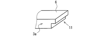
図7に示すように、実施の形態4においては、リード端子3aの長手方向の端部11は段付き形状に形成されている。より具体的には、リード端子3aの直線部の長手方向の端部11は、上側部分よりも下側部分の長手方向の長さが短くなる一段の段付き形状に形成されている。
As shown in FIG. 7, in the fourth embodiment, the
リード端子3aの直線部6の長手方向の端部11を段付き形状とすることで、リード端子3aの長手方向端部の角部に集中する応力を、段付き形状の端部11の角部に分散することができ、封止樹脂5に発生する応力を減少させることができる。
By forming the
以上のように、実施の形態4に係る半導体装置では、リード端子3aの長手方向の端部11は段付き形状に形成されるため、リード端子3aの長手方向端部の角部に集中する応力に起因して封止樹脂5に発生する応力を緩和することができる。また、リード端子3aの直線部6の長手方向の端部11を段付き形状とすることで、リード端子3aの端部11において所定の樹脂厚みを確保することができるため、封止樹脂5の樹脂強度を向上させるとともに、樹脂封止時においてリード端子3aの端部11への樹脂の流動性を確保することができる。
As described above, in the semiconductor device according to the fourth embodiment, since the
なお、図7では、一段の段付き形状を例示したが、多段であってもよい。また、図8に示すように、リード端子3aの直線部6の長手方向の端部11が円弧形状、または図9に示すように、面取り形状に形成されていてもよい。ここで、図8は、実施の形態4の変形例1に係る半導体装置のリード端子3aの部分斜視図であり、図9は、実施の形態4の変形例2に係る半導体装置のリード端子3aの部分斜視図である。これらの場合にも上記と同様の効果が得られる。
In addition, in FIG. 7, although the stepped shape of one step was illustrated, multiple steps may be used. Moreover, as shown in FIG. 8, the
<実施の形態5>
次に、実施の形態5に係る半導体装置について説明する。図10は、実施の形態5に係る半導体装置の部分平面図であり、図11は、実施の形態5に係る半導体装置の部分断面図である。なお、実施の形態5において、実施の形態1から4で説明したものと同一の構成要素については同一符号を付して説明は省略する。
<
Next, a semiconductor device according to the fifth embodiment will be described. FIG. 10 is a partial plan view of the semiconductor device according to the fifth embodiment, and FIG. 11 is a partial cross-sectional view of the semiconductor device according to the fifth embodiment. Note that in the fifth embodiment, the same components as those described in the first to fourth embodiments are denoted by the same reference numerals, and description thereof is omitted.
図10に示すように、実施の形態5においては、リード端子3aは、半導体素子1の上面のうち信号配線12が接続される部分であるワイヤボンドパッド13を除く全上面を覆うように形成されている。より具体的には、実施の形態5においてリード端子3aは、実施の形態1から4の場合よりも平面視輪郭が大きくなるように形成されている。また、リード端子3aのうち、ワイヤボンドパッド13に対応する位置には、ワイヤボンドパッド13が露出するように凹部7cが設けられている。
As shown in FIG. 10, in the fifth embodiment, the
図10に示すように、半導体素子1の上面をリード端子3aで覆うことで、リード端子3aの熱膨張によってリード端子3aの端部から封止樹脂5へ応力が加わる。図11に示すように、万が一クラック8が発生したとしても、半導体素子1上への伝播を避けることができる。また、ワイヤボンドパッド13を限定的に露出させるべく、リード端子3aのうちワイヤボンドパッド13に対応する位置に凹部7cを設けたため、リード端子3aの直線部6を水平方向に部分的に一層分断することができる。
As shown in FIG. 10, by covering the upper surface of the
以上のように、実施の形態5に係る半導体装置では、リード端子3aは、半導体素子1の上面のうち信号配線12が接続される部分を除く全上面を覆うように形成されるため、リード端子3aの熱膨張による応力で封止樹脂5にクラック8が発生した場合でも、リード端子3aによって半導体素子1の上面側にクラック8が進展することを抑制し、半導体素子1へのダメージを抑制できる。また、実施の形態1から4の場合と比較してリード端子3aを大きくすることで、電流密度を下げて、リード端子3aの発熱を低減し熱膨張による影響を軽減することができる。
As described above, in the semiconductor device according to the fifth embodiment, the
<実施の形態6>
次に、実施の形態6に係る半導体装置について説明する。図12は、実施の形態6に係る半導体装置の部分平面図であり、図13は、実施の形態6に係る半導体装置のリード端子3aの構造を示す部分斜視図である。なお、実施の形態6において、実施の形態1から5で説明したものと同一の構成要素については同一符号を付して説明は省略する。
<
Next, a semiconductor device according to the sixth embodiment will be described. FIG. 12 is a partial plan view of the semiconductor device according to the sixth embodiment. FIG. 13 is a partial perspective view showing the structure of the
図12と図13に示すように、実施の形態6においては、リード端子3aは、半導体素子1の上面のうち信号配線12が接続される部分(ワイヤボンドパッド13が存在する部分)に隣接する上面の側へ段付き状に凹んで設けられる凹み部14をさらに備えている。より具体的には、凹み部14は、リード端子3aのうちワイヤボンドパッド13が露出する部分である凹部7cに隣接する位置に段付き状に凹んで設けられている。
As shown in FIGS. 12 and 13, in the sixth embodiment, the
図13においては、リード端子3aのうち凹み部14となる平面部のみを凹ませて凹み部14を形成したが、図14に示すように、ハーフカットを行うことで段付き状の凹み部14を形成してもよい。ここで、図14は、実施の形態6の変形例に係る半導体装置のリード端子3aの構造を示す部分斜視図である。なお、図13と図14においては、図面を見やすくするためにリード端子3aのうち凹み部14から凹部7c側の部分を省略し図示していない。
In FIG. 13, only the flat portion that becomes the recessed
次に、実施の形態6に係る半導体装置の作用、効果について説明する。図15は、実施の形態6に係る半導体装置においてボンディング動作を行っている状態を示す部分平面図であり、図16は、実施の形態6に係る半導体装置においてボンディング動作を行っている状態を示す部分断面図であり、図17は、実施の形態6に係る半導体装置において凹み部14を設けない場合にボンディング動作を行っている状態を示す部分断面図である。
Next, functions and effects of the semiconductor device according to the sixth embodiment will be described. FIG. 15 is a partial plan view showing a state in which the bonding operation is performed in the semiconductor device according to the sixth embodiment, and FIG. 16 shows a state in which the bonding operation is performed in the semiconductor device according to the sixth embodiment. FIG. 17 is a partial cross-sectional view, and FIG. 17 is a partial cross-sectional view showing a state in which a bonding operation is performed when the
図15と図16に示すように、ウェッジツール16によるボンディング動作を行っている状態では、ウェッジツール16の側部がリード端子3aに設けられた段付き状の凹み部14に位置するため、リード端子3aとウェッジツール16との干渉を回避することができる。
As shown in FIGS. 15 and 16, when the bonding operation is performed by the
他方、図17に示すように、リード端子3aに凹み部14を設けない場合、リード端子3aの側面からワイヤボンドパッド13までの距離の関係はc<dとなる。すなわち、凹み部14を設けた場合と同様の位置関係ではウェッジツール16がリード端子3aに干渉することを示している。ここで、cは、凹み部14を設けた場合におけるリード端子3aの側面からワイヤボンドパッド13までの距離であり、dは、凹み部14を設けない場合におけるリード端子3aの側面からワイヤボンドパッド13までの距離である。
On the other hand, as shown in FIG. 17, when the
リード端子3aに凹み部14を設けることで、リード端子3aとウェッジツール16との干渉を回避することができるため、凹部7cを最小限の大きさにすることができ、半導体素子1をリード端子3aで覆う面積を広くすることができる。また、凹み部14によってリード端子3aの直線部6を部分的に分断することができ、封止樹脂5に発生する応力の伝播を分断することができる。
By providing the
以上のように、実施の形態6に係る半導体装置では、リード端子3aは、半導体素子1の上面のうち信号配線12が接続される部分に隣接する上面の側へ段付き状に凹んで設けられる凹み部14をさらに備える。したがって、凹部7cを最小限の大きさにすることができる。また、凹み部14にハーフカットを行った場合はリード端子3a全体を絶縁基板4aから離すことができるため、リード端子3aと絶縁基板4aのクリアランスが広がることで樹脂流動性を確保することができる。
As described above, in the semiconductor device according to the sixth embodiment, the
<実施の形態7>
次に、実施の形態7に係る半導体装置について説明する。図18は、実施の形態7に係る半導体装置の部分斜視図であり、図19は、実施の形態7に係る半導体装置の部分断面図である。なお、実施の形態7において、実施の形態1から6で説明したものと同一の構成要素については同一符号を付して説明は省略する。
<Embodiment 7>
Next, a semiconductor device according to the seventh embodiment will be described. FIG. 18 is a partial perspective view of the semiconductor device according to the seventh embodiment, and FIG. 19 is a partial cross-sectional view of the semiconductor device according to the seventh embodiment. Note that in the seventh embodiment, the same components as those described in the first to sixth embodiments are denoted by the same reference numerals, and description thereof is omitted.
図18に示すように、実施の形態7においては、リード端子3aのうち半導体素子1に接続される部分の側面にロウ材2の濡れ性を向上させる表面処理が施されている。この表面処理は、例えばNiめっきによる処理であり、リード端子3aのうち半導体素子1に接続される部分の側面にはNi薄膜17が形成されている。ここで、表面処理は、Niめっきによる処理以外に、Auめっき、Agめっきまたはフラックスなどによる処理であってもよい。さらに、表面処理は、化学研磨などの表面改質による処理であってもよい。
As shown in FIG. 18, in the seventh embodiment, a surface treatment for improving the wettability of the
図19に示すように、リード端子3aのうち半導体素子1に接続される部分の側面の濡れ性を向上させることで、半導体素子1を接合するためのロウ材2が当該側面に濡れ上がる。ロウ材2と封止樹脂5は密着性が低いため、ロウ材2と封止樹脂5との間に界面18が発生し、これにより、封止樹脂5に生じる応力を分散することができる。
As shown in FIG. 19, by improving the wettability of the side surface of the portion connected to the
以上のように、実施の形態7に係る半導体装置では、リード端子3aのうち半導体素子1に接続される部分の側面に濡れ性を向上させる表面処理が施されるため、半導体素子1を接合するためのロウ材2が当該側面に濡れ上がり、リード端子3aの当該側面と封止樹脂5との密着性が低下する。これにより、リード端子3aの熱膨張による変位から封止樹脂5が分離され、封止樹脂5に応力が発生することを低減できる。
As described above, in the semiconductor device according to the seventh embodiment, since the surface treatment for improving the wettability is performed on the side surface of the portion connected to the
<実施の形態8>
次に、実施の形態8に係る半導体装置について説明する。図20は、実施の形態8に係る半導体装置の部分断面図である。なお、実施の形態8において、実施の形態1から7で説明したものと同一の構成要素については同一符号を付して説明は省略する。
<Eighth embodiment>
Next, a semiconductor device according to the eighth embodiment will be described. FIG. 20 is a partial cross-sectional view of the semiconductor device according to the eighth embodiment. Note that in the eighth embodiment, the same components as those described in the first to seventh embodiments are denoted by the same reference numerals, and description thereof is omitted.
図20に示すように、実施の形態8においては、半導体装置は、リード端子3aのうち半導体素子1に接続される部分の側面を覆う端子カバー19をさらに備えている。より具体的には、端子カバー19は、テフロン(登録商標)樹脂でU字形状に形成され、リード端子3aのうち半導体素子1に接続される部分の側面を含む側部に取り付けられている。ここで、端子カバー19は、テフロン(登録商標)樹脂以外にも、ABS、PC、PSまたはPPSなどの熱可塑性樹脂、またはSUS304などの金属材料を用いて構成することができる。
As shown in FIG. 20, in the eighth embodiment, the semiconductor device further includes a
リード端子3aの側部に端子カバー19を取り付けた後、封止樹脂5を充填することでリード端子3aの熱膨張または収縮の変位を封止樹脂5から分離させることができる。そのため、封止樹脂5に伝播する応力を最小限にすることができる。よって、封止樹脂5のクラック8の発生を抑制する効果が得られる。また、シリコンカーバイトを主とする半導体装置は、一層高温での作動が可能である。すなわち、封止樹脂5を良好な封止状態とすることができるため、一層信頼性の優れた半導体装置を提供することができる。
After the
以上のように、実施の形態8に係る半導体装置は、リード端子3aのうち半導体素子1に接続される部分の側面を覆う端子カバー19をさらに備えるため、リード端子3aと封止樹脂5との間に界面を意図的に作ることで、封止樹脂5に働く応力を減少させることができる。
As described above, since the semiconductor device according to the eighth embodiment further includes the
なお、本発明は、その発明の範囲内において、各実施の形態を自由に組み合わせたり、各実施の形態を適宜、変形、省略することが可能である。 It should be noted that the present invention can be freely combined with each other within the scope of the invention, and each embodiment can be appropriately modified or omitted.
1 半導体素子、3,3a リード端子、5 封止樹脂、7a 凸部、7b 凹部、9スリット、10 ベンド部、12 信号配線、14 凹み部、19 端子カバー。
DESCRIPTION OF
Claims (15)
前記半導体素子の上面に接合されたリード端子と、
前記半導体素子を前記リード端子における前記半導体素子に接合された部分とともに封止する封止樹脂と、
を備え、
前記リード端子は、水平方向に延在する部分を有し、
前記リード端子の前記水平方向に延在する部分は、前記半導体素子に接合されかつ平面視で直線的に延在する部分を含み、
前記リード端子は、前記直線的に延在する部分を平面視において部分的に分断する凹部および凸部を備え、
前記凹部および前記凸部は、平面視で前記半導体素子と重ならない位置に設けられる、半導体装置。 A semiconductor element whose lower surface is bonded to the substrate side;
A lead terminal joined to the upper surface of the semiconductor element;
A sealing resin for sealing the semiconductor element together with a portion of the lead terminal bonded to the semiconductor element;
With
The lead terminal has a portion extending in a horizontal direction,
The portion extending in the horizontal direction of the lead terminal includes a portion joined to the semiconductor element and extending linearly in a plan view,
The lead terminal includes a concave portion and a convex portion that partially divide the linearly extending portion in a plan view,
The said recessed part and the said convex part are semiconductor devices provided in the position which does not overlap with the said semiconductor element by planar view.
前記半導体素子の上面に接合されたリード端子と、
前記半導体素子を前記リード端子における前記半導体素子に接合された部分とともに封止する封止樹脂と、
を備え、
前記リード端子は、水平方向に延在する部分を有し、
前記リード端子の前記水平方向に延在する部分は、前記半導体素子に接合されかつ平面視で直線的に延在する部分を含み、
前記リード端子は、前記直線的に延在する部分を平面視において部分的に分断する一側面側の凹部および他側面側の凹部を備え、
前記一側面側の前記凹部および前記他側面側の前記凹部は、平面視で前記半導体素子と重ならない位置に設けられる、半導体装置。 A semiconductor element whose lower surface is bonded to the substrate side;
A lead terminal joined to the upper surface of the semiconductor element;
A sealing resin for sealing the semiconductor element together with a portion of the lead terminal bonded to the semiconductor element;
With
The lead terminal has a portion extending in a horizontal direction,
The portion extending in the horizontal direction of the lead terminal includes a portion joined to the semiconductor element and extending linearly in a plan view,
The lead terminal includes a concave portion on one side surface and a concave portion on the other side surface partly dividing the linearly extending portion in a plan view,
The semiconductor device, wherein the concave portion on the one side surface side and the concave portion on the other side surface side are provided at positions that do not overlap the semiconductor element in plan view.
前記半導体素子の上面に接合されたリード端子と、
前記半導体素子を前記リード端子における前記半導体素子に接合された部分とともに封止する封止樹脂と、
を備え、
前記リード端子は、水平方向に延在する部分を有し、
前記リード端子の前記水平方向に延在する部分は、前記半導体素子に接合されかつ平面視で直線的に延在する部分を含み、
前記リード端子は、前記直線的に延在する部分を平面視において部分的に分断する凹部または凸部を備え、
前記凹部または前記凸部は、前記リード端子の厚さ以上の幅および奥行きで構成される、半導体装置。 A semiconductor element whose lower surface is bonded to the substrate side;
A lead terminal joined to the upper surface of the semiconductor element;
A sealing resin for sealing the semiconductor element together with a portion of the lead terminal bonded to the semiconductor element;
With
The lead terminal has a portion extending in a horizontal direction,
The portion extending in the horizontal direction of the lead terminal includes a portion joined to the semiconductor element and extending linearly in a plan view,
The lead terminal includes a concave portion or a convex portion that partially divides the linearly extending portion in a plan view,
The said recessed part or the said convex part is a semiconductor device comprised by the width | variety and depth more than the thickness of the said lead terminal.
前記半導体素子の上面に接合され、所定の厚さを有し、長手方向の端部の形状が、前記所定の厚さよりも薄い段付き形状に形成されたリード端子と、
前記半導体素子を前記リード端子の前記段付き形状の部分とともに封止する封止樹脂と、
を備え、
前記段付き形状は、上側部分よりも下側部分の長手方向の長さが短い、半導体装置。 A semiconductor element whose lower surface is bonded to the substrate side;
A lead terminal bonded to the upper surface of the semiconductor element, having a predetermined thickness, and having a shape of a longitudinal end portion thinner than the predetermined thickness;
Sealing resin for sealing the semiconductor element together with the stepped shape portion of the lead terminal;
Equipped with a,
The stepped shape is a semiconductor device in which the length in the longitudinal direction of the lower part is shorter than the upper part .
前記半導体素子の上面に接合され、長手方向の端部の形状が、上側部分よりも下側部分の長手方向の長さが短い多段の段付き形状に形成されたリード端子と、
前記半導体素子を前記リード端子の前記多段の段付き形状の部分とともに封止する封止樹脂と、
を備える、半導体装置。 A semiconductor element whose lower surface is bonded to the substrate side;
A lead terminal joined to the upper surface of the semiconductor element, and the shape of the end portion in the longitudinal direction is formed in a multistage stepped shape in which the length in the longitudinal direction of the lower portion is shorter than the upper portion,
Sealing resin for sealing the semiconductor element together with the multi-stepped portion of the lead terminal;
A semiconductor device comprising:
前記半導体素子の上面に接合され、長手方向の端部の形状が、面取り形状に形成されたリード端子と、
前記半導体素子を前記リード端子の前記面取り形状の部分とともに封止する封止樹脂と、
を備え、
前記面取り形状の面取り部は、前記リード端子の下側部分に設けられる、半導体装置。 A semiconductor element whose lower surface is bonded to the substrate side;
A lead terminal joined to the upper surface of the semiconductor element, and the shape of the end portion in the longitudinal direction is formed in a chamfered shape;
Sealing resin for sealing the semiconductor element together with the chamfered portion of the lead terminal;
Equipped with a,
The chamfered chamfered portion is a semiconductor device provided in a lower portion of the lead terminal .
前記半導体素子の上面に接合されたリード端子と、
前記半導体素子を前記リード端子における前記半導体素子に接合された部分とともに封止する封止樹脂と、
を備え、
前記リード端子は、前記半導体素子の前記上面のうち信号配線が接続される部分を除く全上面を覆うように形成され、
前記リード端子は、前記半導体素子の前記上面のうち信号配線が接続される部分に隣接する前記上面の側へ段付き状に凹んで設けられる凹み部をさらに備える、半導体装置。 A semiconductor element whose lower surface is bonded to the substrate side;
A lead terminal joined to the upper surface of the semiconductor element;
A sealing resin for sealing the semiconductor element together with a portion of the lead terminal bonded to the semiconductor element;
With
The lead terminal is formed so as to cover the entire upper surface of the upper surface of the semiconductor element except for a portion to which a signal wiring is connected,
The lead terminal further includes a recess provided in a stepped manner on the side of the upper surface adjacent to a portion to which a signal wiring is connected in the upper surface of the semiconductor element.
前記半導体素子の上面に接合されたリード端子と、
前記半導体素子を前記リード端子における前記半導体素子に接合された部分とともに封止する封止樹脂と、
を備え、
前記リード端子のうち前記半導体素子に接続される部分の側面を覆う端子カバーをさらに備える、半導体装置。 A semiconductor element whose lower surface is bonded to the substrate side;
A lead terminal joined to the upper surface of the semiconductor element;
A sealing resin for sealing the semiconductor element together with a portion of the lead terminal bonded to the semiconductor element;
With
A semiconductor device further comprising: a terminal cover that covers a side surface of a portion of the lead terminal connected to the semiconductor element.
Priority Applications (6)
| Application Number | Priority Date | Filing Date | Title |
|---|---|---|---|
| JP2014211424A JP6385234B2 (en) | 2014-10-16 | 2014-10-16 | Semiconductor device |
| US14/790,682 US9917064B2 (en) | 2014-10-16 | 2015-07-02 | Semiconductor device with a plate-shaped lead terminal |
| DE102015215786.5A DE102015215786A1 (en) | 2014-10-16 | 2015-08-19 | Semiconductor device |
| CN201510673980.6A CN105529319B (en) | 2014-10-16 | 2015-10-16 | Semiconductor device |
| CN201611055874.2A CN106952877B (en) | 2014-10-16 | 2015-10-16 | Semiconductor device with a plurality of semiconductor chips |
| CN201910281594.0A CN110071072B (en) | 2014-10-16 | 2015-10-16 | Semiconductor device with a semiconductor device having a plurality of semiconductor chips |
Applications Claiming Priority (1)
| Application Number | Priority Date | Filing Date | Title |
|---|---|---|---|
| JP2014211424A JP6385234B2 (en) | 2014-10-16 | 2014-10-16 | Semiconductor device |
Publications (3)
| Publication Number | Publication Date |
|---|---|
| JP2016082048A JP2016082048A (en) | 2016-05-16 |
| JP2016082048A5 JP2016082048A5 (en) | 2016-12-22 |
| JP6385234B2 true JP6385234B2 (en) | 2018-09-05 |
Family
ID=55638195
Family Applications (1)
| Application Number | Title | Priority Date | Filing Date |
|---|---|---|---|
| JP2014211424A Active JP6385234B2 (en) | 2014-10-16 | 2014-10-16 | Semiconductor device |
Country Status (4)
| Country | Link |
|---|---|
| US (1) | US9917064B2 (en) |
| JP (1) | JP6385234B2 (en) |
| CN (3) | CN110071072B (en) |
| DE (1) | DE102015215786A1 (en) |
Families Citing this family (10)
| Publication number | Priority date | Publication date | Assignee | Title |
|---|---|---|---|---|
| US10204847B2 (en) * | 2016-10-06 | 2019-02-12 | Infineon Technologies Americas Corp. | Multi-phase common contact package |
| DE112016007432B4 (en) | 2016-11-11 | 2023-06-22 | Mitsubishi Electric Corporation | semiconductor device, inverter unit and automobile |
| JP6776840B2 (en) * | 2016-11-21 | 2020-10-28 | オムロン株式会社 | Electronic devices and their manufacturing methods |
| JP6806170B2 (en) * | 2017-02-09 | 2021-01-06 | 三菱電機株式会社 | Semiconductor equipment and power conversion equipment |
| WO2018150556A1 (en) * | 2017-02-20 | 2018-08-23 | 新電元工業株式会社 | Electronic device, and connector |
| JP6742540B2 (en) * | 2017-12-13 | 2020-08-19 | 三菱電機株式会社 | Semiconductor device and power conversion device |
| EP3832705A4 (en) * | 2018-11-30 | 2021-09-15 | Hitachi Metals, Ltd. | Electrical connection member, electrical connection structure, and method for producing electrical connection member |
| US11387210B2 (en) * | 2019-03-15 | 2022-07-12 | Fuji Electric Co., Ltd. | Semiconductor module and manufacturing method therefor |
| JP7301805B2 (en) | 2020-09-24 | 2023-07-03 | 株式会社東芝 | semiconductor module |
| WO2023203688A1 (en) * | 2022-04-20 | 2023-10-26 | 三菱電機株式会社 | Semiconductor device and production method for semiconductor device |
Family Cites Families (24)
| Publication number | Priority date | Publication date | Assignee | Title |
|---|---|---|---|---|
| JPH01276655A (en) | 1988-04-27 | 1989-11-07 | Japan Radio Co Ltd | Transfer mold type integrated circuit |
| JPH065742A (en) | 1992-06-22 | 1994-01-14 | Mitsubishi Electric Corp | Semiconductor device, resin used used for sealing and manufacture of the device |
| JPH06120406A (en) | 1992-10-02 | 1994-04-28 | Mitsubishi Electric Corp | Semiconductor device |
| JP3866880B2 (en) | 1999-06-28 | 2007-01-10 | 株式会社日立製作所 | Resin-sealed electronic device |
| JP2005012085A (en) * | 2003-06-20 | 2005-01-13 | Toyota Motor Corp | Electrode structure of semiconductor module |
| JP4628687B2 (en) * | 2004-03-09 | 2011-02-09 | ルネサスエレクトロニクス株式会社 | Semiconductor device |
| JP4468115B2 (en) * | 2004-08-30 | 2010-05-26 | 株式会社ルネサステクノロジ | Semiconductor device |
| CN100442483C (en) | 2004-09-16 | 2008-12-10 | 夏普株式会社 | Optical semiconductor device, method for fabricating the same, lead frame and electronic equipment |
| DE102005043928B4 (en) * | 2004-09-16 | 2011-08-18 | Sharp Kk | Optical semiconductor device and method for its production |
| JP4348267B2 (en) | 2004-09-22 | 2009-10-21 | シャープ株式会社 | Optical semiconductor device, optical communication device, and electronic equipment |
| TWI280673B (en) * | 2004-09-22 | 2007-05-01 | Sharp Kk | Optical semiconductor device, optical communication device, and electronic equipment |
| JP4492448B2 (en) | 2005-06-15 | 2010-06-30 | 株式会社日立製作所 | Semiconductor power module |
| JP4455488B2 (en) * | 2005-12-19 | 2010-04-21 | 三菱電機株式会社 | Semiconductor device |
| JP4349364B2 (en) * | 2005-12-26 | 2009-10-21 | 三菱電機株式会社 | Semiconductor device |
| JP2008016529A (en) * | 2006-07-04 | 2008-01-24 | Renesas Technology Corp | Semiconductor device |
| JP2008218688A (en) * | 2007-03-05 | 2008-09-18 | Denso Corp | Semiconductor device |
| JP5384913B2 (en) * | 2008-11-18 | 2014-01-08 | ルネサスエレクトロニクス株式会社 | Semiconductor device and manufacturing method thereof |
| JP5218009B2 (en) * | 2008-12-16 | 2013-06-26 | 富士電機株式会社 | Semiconductor device |
| JP5251991B2 (en) * | 2011-01-14 | 2013-07-31 | トヨタ自動車株式会社 | Semiconductor module |
| JP5665572B2 (en) | 2011-01-28 | 2015-02-04 | 三菱電機株式会社 | Semiconductor device and manufacturing method of semiconductor device |
| WO2013046400A1 (en) * | 2011-09-29 | 2013-04-04 | トヨタ自動車株式会社 | Semiconductor device |
| JP2013197573A (en) | 2012-03-23 | 2013-09-30 | Mitsubishi Electric Corp | Semiconductor device |
| CN103545268B (en) * | 2012-07-09 | 2016-04-13 | 万国半导体股份有限公司 | The power device of bottom source and preparation method |
| JP6230238B2 (en) * | 2013-02-06 | 2017-11-15 | 三菱電機株式会社 | Semiconductor device and manufacturing method thereof |
-
2014
- 2014-10-16 JP JP2014211424A patent/JP6385234B2/en active Active
-
2015
- 2015-07-02 US US14/790,682 patent/US9917064B2/en active Active
- 2015-08-19 DE DE102015215786.5A patent/DE102015215786A1/en active Pending
- 2015-10-16 CN CN201910281594.0A patent/CN110071072B/en active Active
- 2015-10-16 CN CN201510673980.6A patent/CN105529319B/en active Active
- 2015-10-16 CN CN201611055874.2A patent/CN106952877B/en active Active
Also Published As
| Publication number | Publication date |
|---|---|
| US9917064B2 (en) | 2018-03-13 |
| JP2016082048A (en) | 2016-05-16 |
| CN106952877A (en) | 2017-07-14 |
| CN110071072B (en) | 2023-12-01 |
| CN106952877B (en) | 2021-01-01 |
| DE102015215786A1 (en) | 2016-04-21 |
| CN110071072A (en) | 2019-07-30 |
| CN105529319A (en) | 2016-04-27 |
| CN105529319B (en) | 2019-04-26 |
| US20160111379A1 (en) | 2016-04-21 |
Similar Documents
| Publication | Publication Date | Title |
|---|---|---|
| JP6385234B2 (en) | Semiconductor device | |
| JP6193510B2 (en) | Lead frame, semiconductor device, lead frame manufacturing method, and semiconductor device manufacturing method | |
| JP5966979B2 (en) | Semiconductor device and manufacturing method thereof | |
| JP5414644B2 (en) | Semiconductor device | |
| JP2015070107A (en) | Semiconductor device and manufacturing method of the same | |
| JP2016018866A (en) | Power module | |
| JP6366723B2 (en) | Semiconductor device and manufacturing method thereof | |
| JP6461431B2 (en) | Semiconductor device | |
| JP2014017318A (en) | Semiconductor device | |
| JP6395530B2 (en) | Semiconductor device | |
| JP2008016469A (en) | Semiconductor device | |
| JP6092645B2 (en) | Semiconductor device | |
| JP6129090B2 (en) | Power module and method for manufacturing power module | |
| WO2015125772A1 (en) | Electrode lead and semiconductor device | |
| US9620442B2 (en) | Semiconductor device | |
| JP2006344841A (en) | Power semiconductor module | |
| JP2012238749A (en) | Semiconductor device | |
| JP5602703B2 (en) | Power semiconductor module | |
| JP5793295B2 (en) | Semiconductor device | |
| JP6702431B2 (en) | Semiconductor device | |
| JP4870204B2 (en) | Power semiconductor module | |
| JP5124329B2 (en) | Semiconductor device | |
| JP5477260B2 (en) | Electronic device and manufacturing method thereof | |
| JP7095641B2 (en) | Semiconductor device | |
| JP2022077623A (en) | Lead frame, semiconductor device, and method for manufacturing semiconductor device |
Legal Events
| Date | Code | Title | Description |
|---|---|---|---|
| A521 | Request for written amendment filed |
Free format text: JAPANESE INTERMEDIATE CODE: A523 Effective date: 20161102 |
|
| A621 | Written request for application examination |
Free format text: JAPANESE INTERMEDIATE CODE: A621 Effective date: 20161117 |
|
| A977 | Report on retrieval |
Free format text: JAPANESE INTERMEDIATE CODE: A971007 Effective date: 20170807 |
|
| A131 | Notification of reasons for refusal |
Free format text: JAPANESE INTERMEDIATE CODE: A131 Effective date: 20170822 |
|
| A521 | Request for written amendment filed |
Free format text: JAPANESE INTERMEDIATE CODE: A523 Effective date: 20171020 |
|
| A131 | Notification of reasons for refusal |
Free format text: JAPANESE INTERMEDIATE CODE: A131 Effective date: 20180403 |
|
| A521 | Request for written amendment filed |
Free format text: JAPANESE INTERMEDIATE CODE: A523 Effective date: 20180524 |
|
| TRDD | Decision of grant or rejection written | ||
| A01 | Written decision to grant a patent or to grant a registration (utility model) |
Free format text: JAPANESE INTERMEDIATE CODE: A01 Effective date: 20180710 |
|
| A61 | First payment of annual fees (during grant procedure) |
Free format text: JAPANESE INTERMEDIATE CODE: A61 Effective date: 20180807 |
|
| R150 | Certificate of patent or registration of utility model |
Ref document number: 6385234 Country of ref document: JP Free format text: JAPANESE INTERMEDIATE CODE: R150 |
|
| R250 | Receipt of annual fees |
Free format text: JAPANESE INTERMEDIATE CODE: R250 |
|
| R250 | Receipt of annual fees |
Free format text: JAPANESE INTERMEDIATE CODE: R250 |
|
| R250 | Receipt of annual fees |
Free format text: JAPANESE INTERMEDIATE CODE: R250 |