JP6372084B2 - Light emitting device and electronic device - Google Patents
Light emitting device and electronic device Download PDFInfo
- Publication number
- JP6372084B2 JP6372084B2 JP2014009767A JP2014009767A JP6372084B2 JP 6372084 B2 JP6372084 B2 JP 6372084B2 JP 2014009767 A JP2014009767 A JP 2014009767A JP 2014009767 A JP2014009767 A JP 2014009767A JP 6372084 B2 JP6372084 B2 JP 6372084B2
- Authority
- JP
- Japan
- Prior art keywords
- transistor
- gate electrode
- light emitting
- plan
- wiring
- Prior art date
- Legal status (The legal status is an assumption and is not a legal conclusion. Google has not performed a legal analysis and makes no representation as to the accuracy of the status listed.)
- Active
Links
- 238000005401 electroluminescence Methods 0.000 claims description 2
- 239000010410 layer Substances 0.000 description 193
- 239000004020 conductor Substances 0.000 description 36
- 238000000034 method Methods 0.000 description 21
- 239000004065 semiconductor Substances 0.000 description 17
- 239000000758 substrate Substances 0.000 description 16
- 239000010408 film Substances 0.000 description 13
- 239000003990 capacitor Substances 0.000 description 12
- 230000000149 penetrating effect Effects 0.000 description 11
- 239000002346 layers by function Substances 0.000 description 10
- 230000003287 optical effect Effects 0.000 description 10
- 238000010586 diagram Methods 0.000 description 8
- 238000002955 isolation Methods 0.000 description 7
- 238000000059 patterning Methods 0.000 description 7
- 230000002093 peripheral effect Effects 0.000 description 7
- 239000000463 material Substances 0.000 description 6
- 230000005540 biological transmission Effects 0.000 description 5
- 238000005530 etching Methods 0.000 description 5
- 239000012535 impurity Substances 0.000 description 5
- 229910052581 Si3N4 Inorganic materials 0.000 description 4
- VYPSYNLAJGMNEJ-UHFFFAOYSA-N Silicium dioxide Chemical compound O=[Si]=O VYPSYNLAJGMNEJ-UHFFFAOYSA-N 0.000 description 4
- 230000003071 parasitic effect Effects 0.000 description 4
- 150000003377 silicon compounds Chemical class 0.000 description 4
- HQVNEWCFYHHQES-UHFFFAOYSA-N silicon nitride Chemical compound N12[Si]34N5[Si]62N3[Si]51N64 HQVNEWCFYHHQES-UHFFFAOYSA-N 0.000 description 4
- 229910052814 silicon oxide Inorganic materials 0.000 description 4
- 229910052709 silver Inorganic materials 0.000 description 4
- 239000004332 silver Substances 0.000 description 4
- 101100015456 Litomosoides carinii GP22 gene Proteins 0.000 description 3
- 101710157310 Tegument protein UL47 homolog Proteins 0.000 description 3
- 229910052782 aluminium Inorganic materials 0.000 description 3
- XAGFODPZIPBFFR-UHFFFAOYSA-N aluminium Chemical compound [Al] XAGFODPZIPBFFR-UHFFFAOYSA-N 0.000 description 3
- 239000000969 carrier Substances 0.000 description 3
- 230000000694 effects Effects 0.000 description 3
- 229910010272 inorganic material Inorganic materials 0.000 description 3
- 239000011147 inorganic material Substances 0.000 description 3
- 239000002356 single layer Substances 0.000 description 3
- 238000009751 slip forming Methods 0.000 description 3
- 101001071145 Homo sapiens Polyhomeotic-like protein 1 Proteins 0.000 description 2
- 102100033222 Polyhomeotic-like protein 1 Human genes 0.000 description 2
- 239000008186 active pharmaceutical agent Substances 0.000 description 2
- 230000015572 biosynthetic process Effects 0.000 description 2
- 230000000052 comparative effect Effects 0.000 description 2
- 238000001312 dry etching Methods 0.000 description 2
- 230000005684 electric field Effects 0.000 description 2
- 238000009434 installation Methods 0.000 description 2
- 239000011159 matrix material Substances 0.000 description 2
- 238000001039 wet etching Methods 0.000 description 2
- FYYHWMGAXLPEAU-UHFFFAOYSA-N Magnesium Chemical compound [Mg] FYYHWMGAXLPEAU-UHFFFAOYSA-N 0.000 description 1
- NRTOMJZYCJJWKI-UHFFFAOYSA-N Titanium nitride Chemical compound [Ti]#N NRTOMJZYCJJWKI-UHFFFAOYSA-N 0.000 description 1
- 239000000956 alloy Substances 0.000 description 1
- 229910045601 alloy Inorganic materials 0.000 description 1
- 239000000470 constituent Substances 0.000 description 1
- 230000018109 developmental process Effects 0.000 description 1
- 230000005669 field effect Effects 0.000 description 1
- 230000012447 hatching Effects 0.000 description 1
- 230000005525 hole transport Effects 0.000 description 1
- 238000003384 imaging method Methods 0.000 description 1
- AMGQUBHHOARCQH-UHFFFAOYSA-N indium;oxotin Chemical compound [In].[Sn]=O AMGQUBHHOARCQH-UHFFFAOYSA-N 0.000 description 1
- 238000002347 injection Methods 0.000 description 1
- 239000007924 injection Substances 0.000 description 1
- 239000011810 insulating material Substances 0.000 description 1
- 150000002500 ions Chemical class 0.000 description 1
- 229910052749 magnesium Inorganic materials 0.000 description 1
- 239000011777 magnesium Substances 0.000 description 1
- 229910044991 metal oxide Inorganic materials 0.000 description 1
- 150000004706 metal oxides Chemical class 0.000 description 1
- 239000000203 mixture Substances 0.000 description 1
- 238000007650 screen-printing Methods 0.000 description 1
- 238000007789 sealing Methods 0.000 description 1
- 238000000926 separation method Methods 0.000 description 1
- 229910052710 silicon Inorganic materials 0.000 description 1
- 239000010703 silicon Substances 0.000 description 1
- 238000001228 spectrum Methods 0.000 description 1
- 238000004544 sputter deposition Methods 0.000 description 1
- 239000010409 thin film Substances 0.000 description 1
- 238000007740 vapor deposition Methods 0.000 description 1
- 230000000007 visual effect Effects 0.000 description 1
Images


Classifications
-
- H—ELECTRICITY
- H10—SEMICONDUCTOR DEVICES; ELECTRIC SOLID-STATE DEVICES NOT OTHERWISE PROVIDED FOR
- H10K—ORGANIC ELECTRIC SOLID-STATE DEVICES
- H10K59/00—Integrated devices, or assemblies of multiple devices, comprising at least one organic light-emitting element covered by group H10K50/00
- H10K59/10—OLED displays
- H10K59/12—Active-matrix OLED [AMOLED] displays
- H10K59/131—Interconnections, e.g. wiring lines or terminals
-
- G—PHYSICS
- G09—EDUCATION; CRYPTOGRAPHY; DISPLAY; ADVERTISING; SEALS
- G09G—ARRANGEMENTS OR CIRCUITS FOR CONTROL OF INDICATING DEVICES USING STATIC MEANS TO PRESENT VARIABLE INFORMATION
- G09G3/00—Control arrangements or circuits, of interest only in connection with visual indicators other than cathode-ray tubes
- G09G3/20—Control arrangements or circuits, of interest only in connection with visual indicators other than cathode-ray tubes for presentation of an assembly of a number of characters, e.g. a page, by composing the assembly by combination of individual elements arranged in a matrix no fixed position being assigned to or needed to be assigned to the individual characters or partial characters
- G09G3/22—Control arrangements or circuits, of interest only in connection with visual indicators other than cathode-ray tubes for presentation of an assembly of a number of characters, e.g. a page, by composing the assembly by combination of individual elements arranged in a matrix no fixed position being assigned to or needed to be assigned to the individual characters or partial characters using controlled light sources
- G09G3/30—Control arrangements or circuits, of interest only in connection with visual indicators other than cathode-ray tubes for presentation of an assembly of a number of characters, e.g. a page, by composing the assembly by combination of individual elements arranged in a matrix no fixed position being assigned to or needed to be assigned to the individual characters or partial characters using controlled light sources using electroluminescent panels
- G09G3/32—Control arrangements or circuits, of interest only in connection with visual indicators other than cathode-ray tubes for presentation of an assembly of a number of characters, e.g. a page, by composing the assembly by combination of individual elements arranged in a matrix no fixed position being assigned to or needed to be assigned to the individual characters or partial characters using controlled light sources using electroluminescent panels semiconductive, e.g. using light-emitting diodes [LED]
- G09G3/3208—Control arrangements or circuits, of interest only in connection with visual indicators other than cathode-ray tubes for presentation of an assembly of a number of characters, e.g. a page, by composing the assembly by combination of individual elements arranged in a matrix no fixed position being assigned to or needed to be assigned to the individual characters or partial characters using controlled light sources using electroluminescent panels semiconductive, e.g. using light-emitting diodes [LED] organic, e.g. using organic light-emitting diodes [OLED]
- G09G3/3225—Control arrangements or circuits, of interest only in connection with visual indicators other than cathode-ray tubes for presentation of an assembly of a number of characters, e.g. a page, by composing the assembly by combination of individual elements arranged in a matrix no fixed position being assigned to or needed to be assigned to the individual characters or partial characters using controlled light sources using electroluminescent panels semiconductive, e.g. using light-emitting diodes [LED] organic, e.g. using organic light-emitting diodes [OLED] using an active matrix
-
- H—ELECTRICITY
- H10—SEMICONDUCTOR DEVICES; ELECTRIC SOLID-STATE DEVICES NOT OTHERWISE PROVIDED FOR
- H10K—ORGANIC ELECTRIC SOLID-STATE DEVICES
- H10K59/00—Integrated devices, or assemblies of multiple devices, comprising at least one organic light-emitting element covered by group H10K50/00
- H10K59/10—OLED displays
- H10K59/12—Active-matrix OLED [AMOLED] displays
- H10K59/121—Active-matrix OLED [AMOLED] displays characterised by the geometry or disposition of pixel elements
- H10K59/1213—Active-matrix OLED [AMOLED] displays characterised by the geometry or disposition of pixel elements the pixel elements being TFTs
-
- G—PHYSICS
- G09—EDUCATION; CRYPTOGRAPHY; DISPLAY; ADVERTISING; SEALS
- G09G—ARRANGEMENTS OR CIRCUITS FOR CONTROL OF INDICATING DEVICES USING STATIC MEANS TO PRESENT VARIABLE INFORMATION
- G09G2300/00—Aspects of the constitution of display devices
- G09G2300/04—Structural and physical details of display devices
- G09G2300/0421—Structural details of the set of electrodes
- G09G2300/0426—Layout of electrodes and connections
-
- G—PHYSICS
- G09—EDUCATION; CRYPTOGRAPHY; DISPLAY; ADVERTISING; SEALS
- G09G—ARRANGEMENTS OR CIRCUITS FOR CONTROL OF INDICATING DEVICES USING STATIC MEANS TO PRESENT VARIABLE INFORMATION
- G09G2300/00—Aspects of the constitution of display devices
- G09G2300/08—Active matrix structure, i.e. with use of active elements, inclusive of non-linear two terminal elements, in the pixels together with light emitting or modulating elements
- G09G2300/0809—Several active elements per pixel in active matrix panels
- G09G2300/0842—Several active elements per pixel in active matrix panels forming a memory circuit, e.g. a dynamic memory with one capacitor
- G09G2300/0861—Several active elements per pixel in active matrix panels forming a memory circuit, e.g. a dynamic memory with one capacitor with additional control of the display period without amending the charge stored in a pixel memory, e.g. by means of additional select electrodes
-
- G—PHYSICS
- G09—EDUCATION; CRYPTOGRAPHY; DISPLAY; ADVERTISING; SEALS
- G09G—ARRANGEMENTS OR CIRCUITS FOR CONTROL OF INDICATING DEVICES USING STATIC MEANS TO PRESENT VARIABLE INFORMATION
- G09G2320/00—Control of display operating conditions
- G09G2320/04—Maintaining the quality of display appearance
- G09G2320/043—Preventing or counteracting the effects of ageing
Landscapes
- Engineering & Computer Science (AREA)
- Physics & Mathematics (AREA)
- Microelectronics & Electronic Packaging (AREA)
- Computer Hardware Design (AREA)
- General Physics & Mathematics (AREA)
- Theoretical Computer Science (AREA)
- Geometry (AREA)
- Electroluminescent Light Sources (AREA)
- Devices For Indicating Variable Information By Combining Individual Elements (AREA)
- Control Of Indicators Other Than Cathode Ray Tubes (AREA)
- Control Of El Displays (AREA)
Description
本発明は、発光装置、及び電子機器に関する。 The present invention relates to a light emitting device and an electronic device.
従来から、電子機器の表示装置として、複数の有機エレクトロルミネッセンス(Electroluminescence,以下、ELと略記する)素子がマトリクス状に配置された発光装置が用いられている(例えば、特許文献1)。
特許文献1では、有機ELを駆動するための回路として、複数のトランジスターを備えた画素回路が記載されている。
Conventionally, a light-emitting device in which a plurality of organic electroluminescence (hereinafter abbreviated as EL) elements are arranged in a matrix is used as a display device of an electronic device (for example, Patent Document 1).
Patent Document 1 describes a pixel circuit including a plurality of transistors as a circuit for driving an organic EL.
しかし、上記のような発光装置では、トランジスターのゲート電極とゲート配線とが同層で形成されていたため、トランジスターと平面視で重ならないように配線を設ける必要があり、画素回路の小型化が困難になっていた。 However, in the light emitting device as described above, since the gate electrode of the transistor and the gate wiring are formed in the same layer, it is necessary to provide wiring so as not to overlap the transistor in plan view, and it is difficult to reduce the size of the pixel circuit. It was.
この問題に対して、ゲート電極と配線とを分け、それぞれ別の層に設ける構成が提案されている(例えば、特許文献2)。
このような構成によれば、トランジスターと平面視で重なる位置に配線を設けることが可能であるため、ゲート電極層が配線を兼ねる場合に比べて、画素回路を小型化できる。
To solve this problem, a configuration has been proposed in which the gate electrode and the wiring are separated and provided in different layers (for example, Patent Document 2).
According to such a structure, since the wiring can be provided at a position overlapping with the transistor in plan view, the pixel circuit can be downsized as compared with the case where the gate electrode layer also serves as the wiring.
しかし、上記のような構成においては、ゲート電極と配線とは、ゲート電極におけるチャネル領域よりも外側に設けられた接続配線用の部分(コンタクトパッド部)において接続されるため、ゲート電極をチャネル領域よりも大きく形成する必要があった。したがって、画素回路の小型化に限界があるという問題があった。 However, in the configuration as described above, the gate electrode and the wiring are connected to each other in a connection wiring portion (contact pad portion) provided outside the channel region in the gate electrode. It was necessary to form larger than. Therefore, there is a problem that there is a limit to downsizing of the pixel circuit.
本発明の一つの態様は、上記問題点に鑑みて成されたものであって、画素回路をより小型化できる発光装置、及びそのような発光装置を備えた電子機器を提供することを目的の一つとする。 One aspect of the present invention is made in view of the above problems, and an object of the present invention is to provide a light emitting device capable of further downsizing a pixel circuit, and an electronic apparatus including such a light emitting device. One.
本発明の発光装置の一つの態様は、第1方向に延在する素子部を備えた第1トランジスターを含む複数のトランジスターと、前記第1トランジスターによって電流が供給される発光素子と、を備える画素回路を備え、前記第1トランジスターのゲート電極には、チャネル領域と平面視で重ならない位置において配線が接続された第1コンタクトパッド部が設けられ、前記複数のトランジスターは、前記第1方向と直交する第2方向において前記第1トランジスターの一方側に配置された複数のトランジスターを含むトランジスター群を含み、前記トランジスター群に含まれたトランジスターは、前記第1方向に並んで設けられ、前記トランジスター群は、チャネル領域と平面視で重なる位置において、ゲート電極に配線が接続されているトランジスターと、ゲート電極に、チャネル領域と平面視で重ならない位置において配線が接続されている第2コンタクトパッド部が設けられたトランジスターと、を含み、前記第1コンタクトパッド部は、前記第2方向において前記トランジスター群側に突出し、前記第2コンタクトパッド部は、前記第2方向において前記第1トランジスター側に突出し、前記第1コンタクトパッド部と前記第2コンタクトパッド部とは、前記第1方向に並んで配置されていることを特徴とする。
本発明の発光装置の一つの態様は、第1トランジスターを含む複数のトランジスターと、前記第1トランジスターによって電流が供給される発光素子と、を備える画素回路を備え、前記複数のトランジスターのうち少なくとも一つは、チャネル領域と平面視で重なる位置において、ゲート電極に配線が接続されていることを特徴とする。
One aspect of the light-emitting device of the present invention is a pixel including a plurality of transistors including a first transistor including an element portion extending in a first direction, and a light-emitting element to which current is supplied by the first transistor. A gate electrode of the first transistor is provided with a first contact pad portion to which wiring is connected at a position not overlapping the channel region in plan view, and the plurality of transistors are orthogonal to the first direction. A transistor group including a plurality of transistors disposed on one side of the first transistor in the second direction, and the transistors included in the transistor group are provided side by side in the first direction, and the transistor group includes: In the position overlapping the channel region in plan view, the wiring connected to the gate electrode And a transistor provided with a second contact pad portion to which a wiring is connected to the gate electrode at a position not overlapping the channel region in plan view, the first contact pad portion in the second direction And the second contact pad portion protrudes toward the first transistor in the second direction, and the first contact pad portion and the second contact pad portion extend in the first direction. It is characterized by being arranged side by side.
One aspect of the light-emitting device of the present invention includes a pixel circuit including a plurality of transistors including a first transistor and a light-emitting element to which current is supplied by the first transistor, and at least one of the plurality of transistors. One feature is that a wiring is connected to the gate electrode at a position overlapping the channel region in plan view.
本発明の発光装置の一つの態様によれば、複数のトランジスターのうち少なくとも一つは、チャネル領域と平面視で重なる位置においてゲート電極に配線が接続されるため、ゲート電極においてチャネル領域よりも外側に接続配線用のコンタクトパッド部を設ける必要がない。そのため、ゲート電極をチャネル領域とほぼ同等の大きさとできる。これにより、本発明の発光装置の一つの態様によれば、画素回路をより小型化できる発光装置が得られる。 According to one embodiment of the light-emitting device of the present invention, at least one of the plurality of transistors is connected to the gate electrode at a position overlapping the channel region in plan view, so that the gate electrode is outside the channel region. There is no need to provide a contact pad portion for connection wiring. Therefore, the gate electrode can be approximately the same size as the channel region. Thereby, according to one aspect of the light emitting device of the present invention, a light emitting device capable of further downsizing the pixel circuit can be obtained.
前記複数のトランジスターは、前記第1トランジスターのゲートと前記第1トランジスターのゲートに信号を入力する信号線との間に設けられた選択トランジスターを含み、前記選択トランジスターは、チャネル領域と平面視で重なる位置において、ゲート電極に配線が接続されている構成としてもよい。
この構成によれば、選択トランジスターを小型化することができ、結果として、画素回路を小型化することができる。
The plurality of transistors include a selection transistor provided between a gate of the first transistor and a signal line for inputting a signal to the gate of the first transistor, and the selection transistor overlaps the channel region in plan view. The wiring may be connected to the gate electrode at the position.
According to this configuration, the selection transistor can be reduced in size, and as a result, the pixel circuit can be reduced in size.
前記複数のトランジスターは、前記第1トランジスターのゲートと前記第1トランジスターの一方の電流端との間に設けられた補償トランジスターを含み、前記補償トランジスターは、チャネル領域と平面視で重なる位置において、ゲート電極に配線が接続されている構成としてもよい。
この構成によれば、補償トランジスターを小型化することができ、結果として、画素回路を小型化することができる。
The plurality of transistors include a compensation transistor provided between a gate of the first transistor and one current terminal of the first transistor, and the compensation transistor is arranged at a position overlapping the channel region in plan view. A configuration in which wiring is connected to the electrodes may be employed.
According to this configuration, the compensation transistor can be reduced in size, and as a result, the pixel circuit can be reduced in size.
前記複数のトランジスターは、前記第1トランジスターと前記発光素子との間に設けられた発光制御トランジスターを含み、前記発光制御トランジスターは、チャネル領域と平面視で重なる位置において、ゲート電極に配線が接続されている構成としてもよい。
この構成によれば、発光制御トランジスターを小型化することができ、結果として、画素回路を小型化することができる。
The plurality of transistors include a light emission control transistor provided between the first transistor and the light emitting element, and the light emission control transistor is connected to a gate electrode at a position overlapping the channel region in plan view. It is good also as composition which has.
According to this configuration, the light emission control transistor can be reduced in size, and as a result, the pixel circuit can be reduced in size.
前記複数のトランジスターは、前記発光素子に所定のリセット電位を給電するリセットトランジスターを含み、前記リセットトランジスターは、チャネル領域と平面視で重なる位置において、ゲート電極に配線が接続されている構成としてもよい。
この構成によれば、リセットトランジスターを小型化することができ、結果として、画素回路を小型化することができる。
The plurality of transistors may include a reset transistor that supplies a predetermined reset potential to the light emitting element, and the reset transistor may have a wiring connected to a gate electrode at a position overlapping the channel region in plan view. .
According to this configuration, the reset transistor can be reduced in size, and as a result, the pixel circuit can be reduced in size.
前記第1トランジスターは、チャネル領域と平面視で重なる位置において、ゲート電極に配線が接続されている構成としてもよい。
この構成によれば、第1トランジスターを小型化することができ、結果として、画素回路を小型化することができる。
The first transistor may be configured such that a wiring is connected to the gate electrode at a position overlapping the channel region in plan view.
According to this configuration, the first transistor can be reduced in size, and as a result, the pixel circuit can be reduced in size.
前記画素回路は、特性補償回路を有している構成としてもよい。
この構成によれば、発光素子に電流を供給する第1トランジスターの閾値電圧のばらつきを抑制することができるため、発光素子に供給される電流を安定化できる。
The pixel circuit may include a characteristic compensation circuit.
According to this configuration, variation in the threshold voltage of the first transistor that supplies current to the light emitting element can be suppressed, and thus the current supplied to the light emitting element can be stabilized.
前記配線は、前記複数のトランジスターと異なる層に設けられている構成としてもよい。
この構成によれば、チャネル領域と平面視で重なる位置において、ゲート電極に配線を接続することが容易である。
The wiring may be provided in a different layer from the plurality of transistors.
According to this configuration, it is easy to connect the wiring to the gate electrode at a position overlapping the channel region in plan view.
前記配線は、前記複数のトランジスターのうち少なくとも二つと平面視において重なる構成としてもよい。
この構成によれば、画素回路をより小型化できる。
The wiring may be configured to overlap with at least two of the plurality of transistors in a plan view.
According to this configuration, the pixel circuit can be further downsized.
本発明の発光装置の一つの態様は、第1方向に延在する素子部を備えた第1トランジスターを含む複数のトランジスターと、前記第1トランジスターによって電流が供給される発光素子と、を備える画素回路を備え、前記第1トランジスターのゲート電極には、チャネル領域と平面視で重ならない位置において配線が接続された第1コンタクトパッド部が設けられ、前記複数のトランジスターは、前記第1方向と直交する第2方向において前記第1トランジスターの一方側に配置された複数のトランジスターを含むトランジスター群を含み、前記トランジスター群に含まれたトランジスターは、前記第1方向に並んで設けられ、前記トランジスター群は、チャネル領域と平面視で重なる位置において、ゲート電極に配線が接続されている第2トランジスターと、ゲート電極に、チャネル領域と平面視で重ならない位置において配線が接続されている第2コンタクトパッド部が設けられたトランジスターと、を含み、前記第1コンタクトパッド部は、前記第2方向において前記トランジスター群側に突出し、前記第2コンタクトパッド部は、前記第2方向において前記第1トランジスター側に突出し、前記第1コンタクトパッド部と前記第2コンタクトパッド部とは、前記第1方向に並んで配置され、前記第2トランジスターは、前記第1トランジスターと前記発光素子との間に設けられていることを特徴とする。
本発明の発光装置の一つの態様は、第1トランジスターを含む複数のトランジスターと、前記第1トランジスターによって電流が供給される発光素子と、を備える画素回路を備え、前記複数のトランジスターは、前記第1トランジスターと前記発光素子との間に設けられた第2トランジスターを含み、前記第2トランジスターは、チャネル領域と平面視で重なる位置において、ゲート電極に配線が接続されていることを特徴とする。
One aspect of the light-emitting device of the present invention is a pixel including a plurality of transistors including a first transistor including an element portion extending in a first direction, and a light-emitting element to which current is supplied by the first transistor. A gate electrode of the first transistor is provided with a first contact pad portion to which wiring is connected at a position not overlapping the channel region in plan view, and the plurality of transistors are orthogonal to the first direction. A transistor group including a plurality of transistors disposed on one side of the first transistor in the second direction, and the transistors included in the transistor group are provided side by side in the first direction, and the transistor group includes: The wiring is connected to the gate electrode at a position overlapping the channel region in plan view. A transistor in which a wiring is connected to the gate electrode at a position that does not overlap the channel region in plan view, and the first contact pad portion includes the second contact pad portion. The second contact pad portion protrudes toward the first transistor in the second direction, and the first contact pad portion and the second contact pad portion extend in the first direction. The second transistor is provided between the first transistor and the light emitting element.
One aspect of the light-emitting device of the present invention includes a pixel circuit including a plurality of transistors including a first transistor and a light-emitting element to which current is supplied by the first transistor, and the plurality of transistors includes the first transistor. A second transistor provided between one transistor and the light emitting element is included, and the second transistor has a wiring connected to the gate electrode at a position overlapping the channel region in plan view.
本発明の発光装置の一つの態様によれば、第2トランジスターが、チャネル領域と平面視で重なる位置において、ゲート電極に配線が接続されているため、第2トランジスターのゲート電極に接続配線用のコンタクトパッド部を設ける必要がなく、ゲート電極を小さくできる。したがって、本発明の発光装置の一つの態様によれば、画素回路をより小型化できる発光装置が得られる。 According to one aspect of the light emitting device of the present invention, since the wiring is connected to the gate electrode at the position where the second transistor overlaps with the channel region in plan view, the wiring for connecting wiring is connected to the gate electrode of the second transistor. There is no need to provide a contact pad portion, and the gate electrode can be made small. Therefore, according to one aspect of the light emitting device of the present invention, a light emitting device capable of further downsizing the pixel circuit can be obtained.
前記ゲート電極における配線が接続されている位置は、前記ゲート電極を挟む一対の電流端のうち高電位となる側の電流端寄りである構成としてもよい。
この構成によれば、トランジスターの閾値電圧のばらつきを抑制できる。
本発明の発光装置の一つの態様は、第1方向に延在する素子部を備えた第1トランジスターを含む複数のトランジスターと、前記第1トランジスターによって電流が供給される発光素子と、を備える画素回路を備え、前記第1トランジスターのゲート電極には、チャネル領域と平面視で重ならない位置において配線が接続された第1コンタクトパッド部が設けられ、前記複数のトランジスターは、前記第1方向と直交する第2方向において前記第1トランジスターの一方側に配置された複数のトランジスターを含むトランジスター群を含み、前記トランジスター群に含まれたトランジスターは、前記第1方向に並んで設けられ、前記トランジスター群は、チャネル領域と平面視で重なる位置において、ゲート電極に配線が接続され、かつ、前記チャネル領域と前記ゲート電極とが平面視でほぼ同じ大きさであるトランジスターと、ゲート電極に、チャネル領域と平面視で重ならない位置において配線が接続されている第2コンタクトパッド部が設けられたトランジスターと、を含み、前記第1コンタクトパッド部は、前記第2方向において前記トランジスター群側に突出し、前記第2コンタクトパッド部は、前記第2方向において前記第1トランジスター側に突出し、前記第1コンタクトパッド部と前記第2コンタクトパッド部とは、前記第1方向に並んで配置されている、ことを特徴とする。
本発明の発光装置の一つの態様は、第1トランジスターを含む複数のトランジスターと、前記第1トランジスターによって電流が供給される発光素子と、を備える画素回路を備え、前記複数のトランジスターのうち少なくとも一つは、チャネル領域と平面視で重なる位置において、ゲート電極に配線が接続され、かつ、前記チャネル領域と前記ゲート電極とが平面視でほぼ同じ大きさである、ことを特徴とする。
本発明の発光装置の一つの態様は、第1方向に延在する素子部を備えた第1トランジスターを含む複数のトランジスターと、前記第1トランジスターによって電流が供給される発光素子と、を備える画素回路を備え、前記第1トランジスターのゲート電極には、チャネル領域と平面視で重ならない位置において配線が接続された第1コンタクトパッド部が設けられ、前記複数のトランジスターは、前記第1方向と直交する第2方向において前記第1トランジスターの一方側に配置された複数のトランジスターを含むトランジスター群を含み、前記トランジスター群に含まれたトランジスターは、前記第1方向に並んで設けられ、前記トランジスター群は、前記第1トランジスターと前記発光素子との間に設けられた第2トランジスターと、ゲート電極に、チャネル領域と平面視で重ならない位置において配線が接続されている第2コンタクトパッド部が設けられたトランジスターと、を含み、前記第1コンタクトパッド部は、前記第2方向において前記トランジスター群側に突出し、前記第2コンタクトパッド部は、前記第2方向において前記第1トランジスター側に突出し、前記第1コンタクトパッド部と前記第2コンタクトパッド部とは、前記第1方向に並んで配置され、前記第2トランジスターは、チャネル領域と平面視で重なる位置において、ゲート電極に配線が接続され、かつ、前記チャネル領域と前記ゲート電極とが平面視でほぼ同じ大きさである、ことを特徴とする。
本発明の発光装置の一つの態様は、第1トランジスターを含む複数のトランジスターと、前記第1トランジスターによって電流が供給される発光素子と、を備える画素回路を備え、前記複数のトランジスターは、前記第1トランジスターと前記発光素子との間に設けられた第2トランジスターを含み、前記第2トランジスターは、チャネル領域と平面視で重なる位置において、ゲート電極に配線が接続され、かつ、前記チャネル領域と前記ゲート電極とが平面視でほぼ同じ大きさである、ことを特徴とする。
The position where the wiring in the gate electrode is connected may be close to the current end on the side having a high potential among the pair of current ends sandwiching the gate electrode.
According to this configuration, variation in the threshold voltage of the transistor can be suppressed.
One aspect of the light-emitting device of the present invention is a pixel including a plurality of transistors including a first transistor including an element portion extending in a first direction, and a light-emitting element to which current is supplied by the first transistor. A gate electrode of the first transistor is provided with a first contact pad portion to which wiring is connected at a position not overlapping the channel region in plan view, and the plurality of transistors are orthogonal to the first direction. A transistor group including a plurality of transistors disposed on one side of the first transistor in the second direction, and the transistors included in the transistor group are provided side by side in the first direction, and the transistor group includes: The wiring is connected to the gate electrode at a position overlapping the channel region in plan view, and the front A transistor in which a channel region and the gate electrode are approximately the same size in plan view, and a transistor in which a second contact pad portion is provided in which a wiring is connected to the gate electrode at a position that does not overlap with the channel region in plan view The first contact pad portion protrudes toward the transistor group in the second direction, and the second contact pad portion protrudes toward the first transistor in the second direction. The pad portion and the second contact pad portion are arranged side by side in the first direction.
One aspect of the light-emitting device of the present invention includes a pixel circuit including a plurality of transistors including a first transistor and a light-emitting element to which current is supplied by the first transistor, and at least one of the plurality of transistors. One is characterized in that a wiring is connected to the gate electrode at a position overlapping the channel region in plan view, and the channel region and the gate electrode are substantially the same size in plan view.
One aspect of the light-emitting device of the present invention is a pixel including a plurality of transistors including a first transistor including an element portion extending in a first direction, and a light-emitting element to which current is supplied by the first transistor. A gate electrode of the first transistor is provided with a first contact pad portion to which wiring is connected at a position not overlapping the channel region in plan view, and the plurality of transistors are orthogonal to the first direction. A transistor group including a plurality of transistors disposed on one side of the first transistor in the second direction, and the transistors included in the transistor group are provided side by side in the first direction, and the transistor group includes: A second transistor provided between the first transistor and the light emitting element; And a transistor provided with a second contact pad portion to which wiring is connected at a position that does not overlap the channel region in plan view, and the first contact pad portion includes the transistor in the second direction. The second contact pad portion protrudes toward the group side, the second contact pad portion protrudes toward the first transistor in the second direction, and the first contact pad portion and the second contact pad portion are arranged side by side in the first direction. The second transistor has a wiring connected to a gate electrode at a position overlapping the channel region in plan view, and the channel region and the gate electrode have substantially the same size in plan view. And
One aspect of the light-emitting device of the present invention includes a pixel circuit including a plurality of transistors including a first transistor and a light-emitting element to which current is supplied by the first transistor, and the plurality of transistors includes the first transistor. A second transistor provided between one transistor and the light emitting element, wherein the second transistor has a wiring connected to a gate electrode at a position overlapping the channel region in plan view, and the channel region and the light emitting element The gate electrode is approximately the same size in plan view.
前記発光素子は、有機エレクトロルミネッセンス素子である構成としてもよい。
この構成によれば、電子機器の表示装置として用いることができる。
The light emitting element may be an organic electroluminescent element.
According to this structure, it can be used as a display device of an electronic device.
本発明の電子機器の一つの態様は、上記の発光装置を備えることを特徴とする。
本発明の電子機器の一つの態様によれば、上記の発光装置を備えているため、電子機器をより小型化できる。
One aspect of an electronic device of the present invention includes the above light-emitting device.
According to one aspect of the electronic device of the present invention, since the light emitting device is provided, the electronic device can be further downsized.
以下、図を参照しながら、本発明の実施形態に係る発光装置及び電子機器について説明する。
なお、本発明の範囲は、以下の実施の形態に限定されるものではなく、本発明の技術的思想の範囲内で任意に変更可能である。また、以下の図面においては、各構成をわかりやすくするために、実際の構造と各構造における縮尺や数等を異ならせる場合がある。
Hereinafter, a light emitting device and an electronic apparatus according to an embodiment of the present invention will be described with reference to the drawings.
The scope of the present invention is not limited to the following embodiment, and can be arbitrarily changed within the scope of the technical idea of the present invention. Moreover, in the following drawings, in order to make each structure easy to understand, the actual structure may be different from the scale, number, or the like in each structure.
[発光装置] [Light emitting device]
(第1実施形態)
図1は、本実施形態の発光装置100を示す平面図である。
本実施形態の発光装置100は、図1に示すように、有機EL材料を利用した発光素子を半導体基板10上に形成した有機EL装置である。発光装置100は、例えば、有機発光ダイオード(OLED:Organic Light Emitting Diode)である。半導体基板10は、シリコン等の半導体材料で形成された板状部材であり、複数の発光素子が形成される基材として利用される。
(First embodiment)
FIG. 1 is a plan view showing a
The
図1に示すように、半導体基板10の表面には、表示領域11と周辺領域12と実装領域13とが設けられている。表示領域11は、複数の画素回路Pが配列された矩形状の領域である。表示領域11には、X方向に延在する複数の走査線(配線)22と、各走査線22に対応してX方向に延在する複数の制御線(配線)24と、X方向と交差するY方向に延在する複数の信号線26と、が形成される。画素回路Pは、複数の走査線22と複数の信号線26との各交差に対応した領域である。したがって、複数の画素回路Pは、X方向およびY方向にわたってマトリクス状に配列される。
As shown in FIG. 1, a display region 11, a peripheral region 12, and a mounting region 13 are provided on the surface of the
周辺領域12は、表示領域11を囲む矩形枠状の領域である。駆動回路30は、周辺領域12に設けられている。駆動回路30は、表示領域11内の各画素回路Pを駆動する回路である。駆動回路30は、2つの走査線駆動回路32と信号線駆動回路34とを含んでいる。発光装置100は、駆動回路30が半導体基板10の表面に直接形成されたトランジスター等の能動素子で構成される回路内蔵型の表示装置である。なお、画像表示に直接寄与しないダミー画素が周辺領域12内に形成されていてもよい。
The peripheral area 12 is a rectangular frame area surrounding the display area 11. The
実装領域13は、周辺領域12を挟んで表示領域11とは反対側(すなわち周辺領域12の外側)の領域に設けられている。実装領域13には、複数の実装端子38が配列されている。制御信号や電源電位は、制御回路や電源回路等の各種の外部回路(図示せず)から実装端子38に供給される。外部回路は、例えば実装領域13に接合された可撓性の配線基板(図示せず)に実装される。
The mounting area 13 is provided in an area opposite to the display area 11 with respect to the peripheral area 12 (that is, outside the peripheral area 12). A plurality of mounting
図2は、表示領域11内の1つの画素回路P11を示す回路図である。
図2に示すように、画素回路Pは、発光素子45、駆動トランジスター(第1トランジスター)TDR、選択トランジスターT1、発光制御トランジスター(第2トランジスター)T2、補償トランジスターT3、リセットトランジスターT4、及び容量素子Cを備える。なお、第1実施形態では、画素回路P11のトランジスターTDR,T1〜T4をPチャネル型のトランジスターで構成するが、Nチャネル型のトランジスターで構成することも可能である。この画素回路P21は、例えば、特開2013−088611号公報の図13乃至図17及びその説明に示す駆動方法のように動作させることが可能である。
FIG. 2 is a circuit diagram showing one pixel circuit P11 in the display area 11. As shown in FIG.
As shown in FIG. 2, the pixel circuit P includes a
発光素子45は、有機EL材料の発光層を含む発光機能層450を画素電極(陽極)451と共通電極(陰極)452との間に介在させた電気光学素子である。画素電極451は画素回路P毎に個別に形成され、共通電極452は複数の画素回路Pにわたって連続して形成される。図2に示すように、発光素子45は、第1電源導電体41と第2電源導電体42とを結ぶ電流経路上に配置される。第1電源導電体41は、高電位側の電源電位VELが供給される電源配線である。第2電源導電体42は、低電位側の電源電位VCTが供給される電源配線である。
The
駆動トランジスターTDRは、第1電源導電体41と第2電源導電体42とを結ぶ電流経路上で発光素子45に対して直列に接続されている。具体的には、駆動トランジスターTDRの一対の電流端のうちの一方(ソース)は、第1電源導電体41に接続されている。駆動トランジスターTDRの一対の電流端のうちの他方(ドレイン)は、発光素子45の画素電極451と接続されている。駆動トランジスターTDRは、自身のゲート−ソース間の電圧に応じた電流量に相当する駆動電流を生成する。
The drive transistor TDR is connected in series to the
図2に示す選択トランジスターT1は、信号線26と駆動トランジスターTDRのゲートとの導通状態(導通/非導通)を制御するスイッチとして機能する。選択トランジスターT1のゲートは走査線22に接続されている。選択トランジスターT1のソースは、信号線26に接続されている。選択トランジスターT1のドレインは、駆動トランジスターTDRのゲートと、発光制御トランジスターT2のドレインと、後述する容量素子Cの第1電極C1と接続されている。
The selection transistor T1 shown in FIG. 2 functions as a switch that controls the conduction state (conduction / non-conduction) between the
なお、後述する特性補償における動作においては、選択トランジスターT1に流れる電流の向きが逆転するため、選択トランジスターT1におけるソースとドレインとの関係は逆となるが、本明細書における実施形態においては、駆動トランジスターのゲートに発光素子の諧調レベルに応じた電位を書き込む期間において、選択トランジスターに流れる電流の向きにおけるソースとドレインとの関係で説明する。 In the characteristic compensation operation described later, since the direction of the current flowing through the selection transistor T1 is reversed, the relationship between the source and the drain in the selection transistor T1 is reversed. However, in the embodiment in the present specification, driving is performed. In the period in which a potential corresponding to the gradation level of the light-emitting element is written to the gate of the transistor, the relationship between the source and the drain in the direction of the current flowing through the selection transistor is described.
発光制御トランジスターT2は、駆動トランジスターTDRと発光素子45との間に直列に接続されている。具体的には、発光制御トランジスターT2のソースは、駆動トランジスターTDRのドレインと接続され、発光制御トランジスターT2のドレインは、発光素子45の画素電極451と接続されている。発光制御トランジスターT2のゲートは、制御線24に接続されている。
The light emission control transistor T2 is connected in series between the drive transistor TDR and the
発光制御トランジスターT2は、制御線24を介して走査線駆動回路32(図1参照)からゲートに入力される制御信号によって、オン/オフが制御される。発光制御トランジスターT2オン状態に制御された状態では、駆動電流が駆動トランジスターTDRから発光制御トランジスターT2を経由して発光素子45に供給される。このとき、発光素子45は、駆動電流の電流量に応じた輝度で発光する。発光制御トランジスターT2がオフ状態に制御された状態では、発光素子45に対する駆動電流の供給が遮断される。このとき、発光素子45は消灯する。
The light emission control transistor T2 is controlled to be turned on / off by a control signal input to the gate from the scanning line driving circuit 32 (see FIG. 1) via the
容量素子Cは、第1電極C1と第2電極C2との間に誘電体を介在させた静電容量である。第1電極C1は、駆動トランジスターTDRのゲートに接続されている。第2電極C2は、第1電源導電体41(駆動トランジスターTDRのソース)に接続されている。したがって、容量素子Cは、駆動トランジスターTDRのゲート−ソース間の電圧を保持する。 The capacitive element C is a capacitance in which a dielectric is interposed between the first electrode C1 and the second electrode C2. The first electrode C1 is connected to the gate of the driving transistor TDR. The second electrode C2 is connected to the first power supply conductor 41 (the source of the driving transistor TDR). Therefore, the capacitive element C holds the voltage between the gate and the source of the driving transistor TDR.
補償トランジスターT3は、駆動トランジスターTDRの閾値電圧のばらつきに起因した発光素子45へ供給される電流値のばらつきを補償するためのトランジスターである。補償トランジスターT3のソースは、駆動トランジスターTDRのドレイン及び発光制御トランジスターT2のソースと接続されている。補償トランジスターT3のドレインは、駆動トランジスターTDRのゲートと接続されている。補償トランジスターT3のゲートには、制御線(配線)23が接続されている。補償トランジスターT3は、制御線23からの制御信号によってオン/オフが制御される。
The compensation transistor T3 is a transistor for compensating for variations in the current value supplied to the
補償トランジスターT3、駆動トランジスターTDR及び選択トランジスターT1がオン状態となると、駆動トランジスターTDRのソース−ドレインに流れる電流が、補償トランジスターT3、選択トランジスターT1を介して、信号線26へと流れる。ここで、本実施形態においては、信号線26には容量素子Cpの第1容量電極Cp1が接続されている。これにより、駆動トランジスターTDRのゲートから容量素子Cpの第1容量電極Cp1までの電位は、駆動トランジスターTDRのソース−ゲート間の電圧が閾値電圧に向けて上昇する。理想的には、駆動トランジスター151のゲートから容量素子Cpの第1容量電極Cp1までの電位は、駆動トランジスター151のソース−ゲート間の電圧が閾値電圧に到達し、駆動トランジスター151のソース−ドレインに流れる電流は流れなくなる。補償トランジスター153がオフの状態となると、この駆動トランジスター151のソース−ゲート間の電圧が容量素子Cに保存される。
When the compensation transistor T3, the drive transistor TDR, and the selection transistor T1 are turned on, a current that flows through the source and drain of the drive transistor TDR flows to the
そして、補償トランジスターT3がオフの状態において、容量素子Cpの第2容量電極Cp2に発光素子45の階調レベルに応じた信号が入力されると、駆動トランジスターTDRのゲートから第1容量電極Cp1までの電位が、階調レベルに応じて上方にシフトする。これにより、駆動トランジスターTDRのソース−ゲート間の電圧値が、閾値電圧に、階調レベルに応じた分の電圧が加えられた値となる。すなわち、駆動トランジスターTDRのソース−ゲート間の電圧が、閾値電圧が補償された値となる。そのため、駆動トランジスターTDRの閾値電圧の値によらず、発光素子45に対して、諧調レベルに応じた電流を安定して供給できる。
When a signal corresponding to the gradation level of the
以上に説明したようにして、駆動トランジスターTDRの閾値電圧特性が補償される。すなわち、画素回路P11は、補償トランジスターT3及び容量素子Cp等によって構成される特性補償回路を有している。 As described above, the threshold voltage characteristics of the drive transistor TDR are compensated. That is, the pixel circuit P11 has a characteristic compensation circuit configured by the compensation transistor T3, the capacitive element Cp, and the like.
リセットトランジスターT4は、発光素子45の電位をリセットするためのトランジスターである。リセットトランジスターT4のソースは、発光制御トランジスターT2のドレイン及び発光素子45の画素電極451に接続されている。リセットトランジスターT4のドレインは、第3電源導電体27に接続されている。第3電源導電体27は、発光素子45がリセットされる電位(リセット電位)が供給される電源配線である。リセットトランジスターT4のゲートは、制御線(配線)25に接続されている。リセットトランジスターT4は、制御線25からの制御信号によってオン/オフが制御される。
The reset transistor T4 is a transistor for resetting the potential of the
発光素子45を初期化する期間においては、リセットトランジスターT4がオン状態となり、発光制御トランジスターT2がオフ状態となる。これにより、発光素子45は、リセットトランジスターT4を介して、第3電源導電体27と接続され、発光素子45の電位は、第3電源導電体27の電位にリセットされる。
In the period in which the
発光素子45には寄生容量が生じる場合があり、寄生容量が生じると、この寄生容量によって発光素子45の画素電極451と共通電極452との間の電圧が保持される。そのため、例えば、発光素子45を高輝度状態から低輝度状態へと転じるような場合においては、寄生容量に高輝度状態における高電圧が保持されてしまうため、発光素子45に過剰な電流が流れ、発光素子45を低輝度状態にすることが困難となる。
これに対して、リセットトランジスターT4によって上記のようにして発光素子45の電位をリセットすることにより、発光素子45を高輝度状態から低輝度状態に転じることが容易となる。
A parasitic capacitance may be generated in the
On the other hand, by resetting the potential of the
図1に示す信号線駆動回路34は、外部回路から供給される画像信号を、画素回路P毎に指定する階調に応じた階調電位(データ信号)として、書込期間(水平走査期間)毎に複数の信号線26に対して並列に供給する。他方、走査線駆動回路32は、複数の走査線22の各々に走査信号を供給することにより、複数の走査線22の各々を書込期間毎に順次選択する。走査線駆動回路32が選択した走査線22に対応する画素回路Pの選択トランジスターT1は、オン状態に遷移する。このとき、各画素回路Pの駆動トランジスターTDRのゲートに、信号線26と選択トランジスターT1とを経由して階調電位が供給され、階調電位に応じた電圧が容量素子Cに保持される。
The signal
他方、書込期間での走査線22の選択が終了すると、走査線駆動回路32は、各制御線24に制御信号を供給することにより、当該制御線24に対応する画素回路Pの発光制御トランジスターT2をオン状態に制御する。したがって、直前の書込期間で容量素子Cに保持された電圧に応じた駆動電流は、駆動トランジスターTDRから発光制御トランジスターT2を経由して発光素子45に供給される。以上のように、発光素子45が階調電位に応じた輝度で発光することで、画像信号が指定する任意の画像が表示領域11に表示される。
On the other hand, when the selection of the
次に、画素回路P11の具体的な構成について説明する。
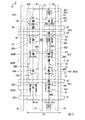
図3は、画素回路P11を模式的に示す平面図である。図4は、図3におけるIV−IV断面図である。図5から図12は、図4における各層を平面視した場合を示す平面図である。図5から図12においては、各要素の視覚的な把握を容易化する観点から、図4と共通する各要素には図4と同様のハッチングが便宜的に付加されている。
Next, a specific configuration of the pixel circuit P11 will be described.
FIG. 3 is a plan view schematically showing the pixel circuit P11. 4 is a cross-sectional view taken along the line IV-IV in FIG. 5 to 12 are plan views showing a case where each layer in FIG. 4 is viewed in plan. 5 to 12, the same hatching as in FIG. 4 is added for convenience to each element common to FIG. 4 from the viewpoint of facilitating visual grasp of each element.
本実施形態においては、各トランジスターは、例えば、MOSFET(Metal Oxide Semiconductor Field Effect Transistor)である。
本実施形態の各トランジスターTDR,T1,T2,T3,T4は、図4に示すように、半導体基板10の表面に形成されている。より詳細には、各トランジスターTDR,T1,T2,T3,T4は、半導体基板10のうちN型の基体16の表面に形成されたP型のウェル17を利用して形成されている。なお、発光制御トランジスターT2及びリセットトランジスターT4については、図4において図示を省略している。
In the present embodiment, each transistor is, for example, a MOSFET (Metal Oxide Semiconductor Field Effect Transistor).
Each transistor TDR, T1, T2, T3, and T4 of this embodiment is formed on the surface of the
駆動トランジスターTDRは、図3に示すように、素子部EDRと、ゲート電極GDRと、を備える。素子部EDRには、ソース領域ASDRと、ドレイン領域ADDRと、チャネル領域ACDRと、が形成されている。 As shown in FIG. 3, the driving transistor TDR includes an element portion EDR and a gate electrode GDR. In the element portion EDR, a source region ASDR, a drain region ADDR, and a channel region ACDR are formed.
選択トランジスターT1は、素子部E1と、ゲート電極G1と、を備える。素子部E1には、ソース領域AS1と、ドレイン領域AD1と、チャネル領域AC1とが形成されている。 The selection transistor T1 includes an element portion E1 and a gate electrode G1. In the element portion E1, a source region AS1, a drain region AD1, and a channel region AC1 are formed.
発光制御トランジスターT2は、素子部E2と、ゲート電極G2と、を備える。素子部E2には、ソース領域AS2と、ドレイン領域AD2と、チャネル領域AC2とが形成されている。 The light emission control transistor T2 includes an element portion E2 and a gate electrode G2. In the element portion E2, a source region AS2, a drain region AD2, and a channel region AC2 are formed.
補償トランジスターT3は、素子部E3と、ゲート電極G3と、を備える。素子部E3には、ソース領域AS3と、ドレイン領域AD3と、チャネル領域AC3とが形成されている。本実施形態においては、補償トランジスターT3のドレイン領域AD3は、選択トランジスターT1のドレイン領域AD1としても機能する。 The compensation transistor T3 includes an element portion E3 and a gate electrode G3. In the element portion E3, a source region AS3, a drain region AD3, and a channel region AC3 are formed. In the present embodiment, the drain region AD3 of the compensation transistor T3 also functions as the drain region AD1 of the selection transistor T1.
リセットトランジスターT4は、素子部E4と、ゲート電極G4と、を備える。素子部E4には、ソース領域AS4と、ドレイン領域AD4と、チャネル領域AC4とが形成されている。 The reset transistor T4 includes an element portion E4 and a gate electrode G4. In the element portion E4, a source region AS4, a drain region AD4, and a channel region AC4 are formed.
なお、本実施形態においては、各トランジスターの構成は同様であるため、以下の説明においては、代表して駆動トランジスターTDRについてのみ説明する場合がある。 In the present embodiment, since the configuration of each transistor is the same, only the drive transistor TDR may be described as a representative in the following description.
素子部EDR,E1,E3は、図3及び図4に示すように、半導体基板10のウェル17に形成されている。図4においては図示を省略するが、発光制御トランジスターT2及びリセットトランジスターT4の素子部E2,E4についても同様である。
The element portions EDR, E1, E3 are formed in the well 17 of the
本実施形態においては、図3及び図4に示すように、選択トランジスターT1の素子部E1と、補償トランジスターT3の素子部E3とは、それぞれのドレイン領域AD1と、ドレイン領域AD3とが共通である。また、図4に示すように、駆動トランジスターTDRの素子部EDRと、選択トランジスターT1及び補償トランジスターT3の素子部E1,E3とは、半導体基板10のウェル17に形成された溝部(トレンチ)10Aにより相互に分離された島状に形成されている。図4においては、図示を省略するが、発光制御トランジスターT2及びリセットトランジスターT4の素子部E2,E4についても同様に相互に分離された島状に形成されている。
In the present embodiment, as shown in FIGS. 3 and 4, the element portion E1 of the selection transistor T1 and the element portion E3 of the compensation transistor T3 have a common drain region AD1 and drain region AD3. . Further, as shown in FIG. 4, the element portion EDR of the driving transistor TDR and the element portions E1 and E3 of the selection transistor T1 and the compensation transistor T3 are formed by a groove portion (trench) 10A formed in the well 17 of the
各素子部を画定する溝部10Aは、半導体基板10の表面に形成されたウェル17を部分的に除去した領域である。
図4に例示された溝部10Aの深さDTは、半導体基板10(ウェル17)の表面と溝部10Aの底面との距離である。溝部10Aの深さDTは、例えば300nm以上かつ1000nm以下の範囲内の寸法(例えば数百nm程度)に設定される。図4から理解される通り、溝部10Aの深さDTはウェル17の厚さDWを下回る(DT<DW)。したがって、溝部10Aの底面はウェル17で構成される。
The
The depth DT of the
溝部10Aの内側(すなわち各素子部の相互間)には、素子分離部54が形成されている。素子分離部54は、各トランジスターを電気的に絶縁(素子分離)するための要素として機能する。すなわち、本実施形態においては、各トランジスターを電気的に分離するSTI(Shallow Trench Isolation)構造の素子分離部54が形成される。具体的には、素子分離部54は、駆動トランジスターTDRと、選択トランジスターT1補償トランジスターT3と、図示は省略するが、発光制御トランジスターT2と、リセットトランジスターT4とを分離する。
An
図4に示すように、本実施形態における素子分離部54の厚さ(溝部10Aの深さ)DTは、ソース領域ASDR及びドレイン領域ADDRの厚さDFを上回る。したがって、素子分離部54の厚さDTがソース領域ASDRまたはドレイン領域ADDRの厚さDFを下回る構成と比較して、相互に隣り合う各トランジスターのソース領域及びドレイン領域の間での電流のリークが抑制される(各トランジスターを確実に分離できる)という利点がある。
As shown in FIG. 4, the thickness (depth of the
本実施形態では、図3及び図5に示すように、各素子部は、平面視(XY面視)でY方向に延在する帯状に形成されている。
駆動トランジスターTDRの素子部EDRと、リセットトランジスターT4の素子部E4とは、長さ方向がY方向となるように配置され、Y方向と平行な仮想直線K1に沿って並んで設けられている。
In the present embodiment, as shown in FIGS. 3 and 5, each element portion is formed in a strip shape extending in the Y direction in plan view (XY plane view).
The element portion EDR of the drive transistor TDR and the element portion E4 of the reset transistor T4 are arranged so that the length direction is the Y direction, and are provided side by side along a virtual straight line K1 parallel to the Y direction.
選択トランジスターT1の素子部E1及び補償トランジスターT3の素子部E3と、発光制御トランジスターT2の素子部E2と、は、長さ方向がY方向となるように配置され、Y方向と平行な仮想直線K2に沿って並んで設けられている。
仮想直線K1と仮想直線K2とは、X方向に並んで設けられている。すなわち、本実施形態の画素回路P11における5つのトランジスターの素子部は、2列に並んで設けられている。
The element part E1 of the selection transistor T1, the element part E3 of the compensation transistor T3, and the element part E2 of the light emission control transistor T2 are arranged so that the length direction is the Y direction, and a virtual straight line K2 parallel to the Y direction. Are arranged side by side.
The virtual straight line K1 and the virtual straight line K2 are provided side by side in the X direction. That is, the element portions of the five transistors in the pixel circuit P11 of the present embodiment are provided in two rows.
なお、本実施形態において、トランジスターにおける素子部の長さ方向とは、後述するソース領域とドレイン領域とが並ぶ方向である。 In the present embodiment, the length direction of the element portion in the transistor is a direction in which a source region and a drain region described later are arranged.
ソース領域ASDR及びドレイン領域ADDRは、図3及び図4に示すように、駆動トランジスターTDRの素子部EDRのうち平面視でゲート電極を挟む各位置に形成された領域である。ソース領域ASDR及びドレイン領域ADDRは、P型のウェル17に対して逆導電型(すなわちN型)の不純物のイオンが導入及び拡散された所定の厚さの領域である。 As shown in FIGS. 3 and 4, the source region ASDR and the drain region ADDR are regions formed at positions where the gate electrode is sandwiched in plan view in the element portion EDR of the drive transistor TDR. The source region ASDR and the drain region ADDR are regions having a predetermined thickness in which ions of impurities of reverse conductivity type (that is, N type) are introduced and diffused into the P type well 17.
素子部EDRが形成された半導体基板10(ウェル17)の面上には、絶縁層50が形成されている。絶縁層50は、例えば珪素化合物(典型的には窒化珪素や酸化珪素)等の絶縁性の無機材料で形成され、絶縁膜52と素子分離部54とを含んで構成される。絶縁膜52は、絶縁層50のうち各素子部の面上に位置する部分であり、各トランジスターのゲート絶縁膜として機能する。
An insulating
ゲート電極GDRは、図4及び図6に示すように、絶縁層50の面上に形成されている。すなわち、素子部EDRとゲート電極GDRとは絶縁膜52(絶縁層50)を挟んで対向する。素子部EDRにおけるソース領域ASDRとドレイン領域ADDRとに挟まれた領域のうち、ゲート電極GDRと平面視で重なる部分が、チャネル領域ACDRとなる。
As shown in FIGS. 4 and 6, the gate electrode GDR is formed on the surface of the insulating
図5及び図6に示すように、駆動トランジスターTDRのチャネル幅WDRは、選択トランジスターT1のチャネル幅W1及び補償トランジスターT3のチャネル幅W2を上回る。本実施形態においては、選択トランジスターT1のチャネル幅W1と補償トランジスターT3のチャネル幅W2とは、ほぼ等しい。駆動トランジスターTDRのチャネル幅WDRは、例えば、500nmである。 As shown in FIGS. 5 and 6, the channel width WDR of the driving transistor TDR is larger than the channel width W1 of the selection transistor T1 and the channel width W2 of the compensation transistor T3. In the present embodiment, the channel width W1 of the selection transistor T1 and the channel width W2 of the compensation transistor T3 are substantially equal. The channel width WDR of the drive transistor TDR is, for example, 500 nm.
駆動トランジスターTDRのゲート電極GDRは、図3に示すように、中継電極QA3を介して、選択トランジスターT1のドレイン領域AD1と電気的に接続されている。本実施形態においては、中継電極(配線)QA3は、コンタクトホールHA8を介して、駆動トランジスターTDRのゲート電極GDRと電気的に接続されている。本実施形態においては、コンタクトホールHA8は、チャネル領域ACDRと平面視で重なる位置に設けられている。言い換えると、駆動トランジスターTDRは、チャネル領域ACDRと平面視で重なる位置において、ゲート電極GDRが中継電極QA3と接続されている。 As shown in FIG. 3, the gate electrode GDR of the driving transistor TDR is electrically connected to the drain region AD1 of the selection transistor T1 via the relay electrode QA3. In the present embodiment, the relay electrode (wiring) QA3 is electrically connected to the gate electrode GDR of the drive transistor TDR via the contact hole HA8. In the present embodiment, the contact hole HA8 is provided at a position overlapping the channel region ACDR in plan view. In other words, in the drive transistor TDR, the gate electrode GDR is connected to the relay electrode QA3 at a position overlapping the channel region ACDR in plan view.
選択トランジスターT1のゲート電極G1は、コンタクトホールHA1を介して、走査線22と電気的に接続されている。走査線22は、駆動トランジスターTDR及び選択トランジスターT1の上方を通過するように、X方向に延在して設けられている。言い換えると、走査線22は、駆動トランジスターTDR及び選択トランジスターT1と平面視において重なるように設けられている。
The gate electrode G1 of the selection transistor T1 is electrically connected to the
コンタクトホールHA1は、チャネル領域AC1と平面視で重なる位置に設けられている。言い換えると、選択トランジスターT1は、チャネル領域AC1と平面視で重なる位置において、ゲート電極G1が走査線22と接続されている。コンタクトホールHA1は、ゲート電極G1におけるソース領域AS1寄り(+Y寄り)の位置に設けられている。
The contact hole HA1 is provided at a position overlapping the channel region AC1 in plan view. In other words, the selection transistor T1 has the gate electrode G1 connected to the
発光制御トランジスターT2のゲート電極G2は、コンタクトホールH2を介して、制御線24と電気的に接続されている。制御線24は、発光制御トランジスターT2及びリセットトランジスターT4の上方を通過するように、X方向に延在して設けられている。言い換えると、制御線24は、発光制御トランジスターT2及びリセットトランジスターT4と平面視において重なるように設けられている。
The gate electrode G2 of the light emission control transistor T2 is electrically connected to the
コンタクトホールH2は、チャネル領域AC2と平面視で重なる位置に設けられている。言い換えると、発光制御トランジスターT2は、チャネル領域AC2と平面視で重なる位置において、ゲート電極G2が制御線24と接続されている。コンタクトホールH2は、ゲート電極G2におけるソース領域AS2寄り(+Y寄り)の位置に設けられている。
The contact hole H2 is provided at a position overlapping the channel region AC2 in plan view. In other words, in the light emission control transistor T2, the gate electrode G2 is connected to the
補償トランジスターT3のゲート電極G3は、コンタクトホールHA2を介して、制御線23と電気的に接続されている。制御線23は、駆動トランジスターTDR及び補償トランジスターT3の上方を通過するように、X方向に延在して設けられている。言い換えると、制御線23は、駆動トランジスターTDR及び補償トランジスターT3と平面視において重なるように設けられている。
The gate electrode G3 of the compensation transistor T3 is electrically connected to the
コンタクトホールHA2は、チャネル領域AC3と平面視で重なる位置に設けられている。言い換えると、補償トランジスターT3は、チャネル領域AC3と平面視で重なる位置において、ゲート電極G3が制御線23と接続されている。コンタクトホールHA2は、ゲート電極G3におけるソース領域AS3寄り(−Y寄り)の位置に設けられている。
The contact hole HA2 is provided at a position overlapping the channel region AC3 in plan view. In other words, the compensation transistor T3 has the gate electrode G3 connected to the
リセットトランジスターT4のゲート電極G4は、コンタクトホールH4を介して、制御線25と電気的に接続されている。制御線25は、発光制御トランジスターT2及びリセットトランジスターT4の上方を通過するように、X方向に延在して設けられている。言い換えると、制御線25は、発光制御トランジスターT2及びリセットトランジスターT4と平面視において重なるように設けられている。
The gate electrode G4 of the reset transistor T4 is electrically connected to the
コンタクトホールH4は、チャネル領域AC4と平面視で重なる位置に設けられている。言い換えると、リセットトランジスターT4は、チャネル領域AC4と平面視で重なる位置において、ゲート電極G4が制御線25と接続されている。コンタクトホールH4は、ゲート電極G4におけるソース領域AS4寄り(−Y寄り)の位置に設けられている。
The contact hole H4 is provided at a position overlapping the channel region AC4 in plan view. In other words, the reset transistor T4 has the gate electrode G4 connected to the
以上に説明した各トランジスターのゲート電極が形成された絶縁層50の面上には、図4に例示される通り、複数の絶縁層L(LA〜LF)と複数の配線層W(WA〜WF)とを交互に積層した多層配線層が形成される。各絶縁層Lは、例えば珪素化合物(典型的には窒化珪素や酸化珪素)等の絶縁性の無機材料で形成される。また、各配線層Wは、アルミニウムや銀等を含有する低抵抗な導電材料で形成される。なお、以下の説明では、導電層(単層または複数層)の選択的な除去により複数の要素が同一工程で一括的に形成される関係を「同層から形成される」と表記する。
On the surface of the insulating
以下、多層配線層について詳細に説明する。
なお、本実施形態においては、多層配線層の説明として、図3におけるIV−IV断面、すなわち、駆動トランジスターTDR、選択トランジスターT1、及び補償トランジスターT3の断面を示す図4を参照して説明する。
Hereinafter, the multilayer wiring layer will be described in detail.
In the present embodiment, the multilayer wiring layer will be described with reference to FIG. 4 showing the IV-IV cross section in FIG. 3, that is, the cross section of the drive transistor TDR, select transistor T1, and compensation transistor T3.
図4の絶縁層LAは、各トランジスターのゲート電極が形成された絶縁層50(絶縁膜52)の面上に形成される。図4及び図7に示すように、絶縁層LAの面上には、走査線22及び制御線23と複数の中継電極QA(QA1〜QA4)とを含む導体パターンが同層(配線層WA)から形成される。上述したように、走査線22は、絶縁層LAを貫通するコンタクトホールHA1を介して選択トランジスターT1のゲート電極G1に導通し、制御線23は、絶縁層LAを貫通するコンタクトホールHA2を介して補償トランジスターT3のゲート電極G3に導通する。
4 is formed on the surface of the insulating layer 50 (insulating film 52) on which the gate electrode of each transistor is formed. As shown in FIGS. 4 and 7, on the surface of the insulating layer LA, a conductor pattern including the
中継電極QA1は、絶縁層LAと絶縁層50とを貫通するコンタクトホールHA3を介して駆動トランジスターTDRのソース領域ASDRに導通する。中継電極QA2は、図4及び図7から理解される通り、絶縁層LAと絶縁層50とを貫通するコンタクトホールHA4を介して駆動トランジスターTDRのドレイン領域ADDRに導通するとともに、絶縁層LAと絶縁層50とを貫通するコンタクトホールHA5を介して補償トランジスターT3のソース領域AS3に導通する。これにより、駆動トランジスターTDRのドレイン領域ADDRと、補償トランジスターT3のソース領域AS3とが接続される。
The relay electrode QA1 is electrically connected to the source region ASDR of the driving transistor TDR through a contact hole HA3 that penetrates the insulating layer LA and the insulating
中継電極QA3は、絶縁層LAと絶縁層50とを貫通するコンタクトホールHA6を介して選択トランジスターT1のドレイン領域AD1及び補償トランジスターT3のドレイン領域AD3に導通するとともに、絶縁層LAを貫通するコンタクトホールHA8を介して駆動トランジスターTDRのゲート電極GDRに導通する。すなわち、駆動トランジスターTDRのゲート電極GDRが、選択トランジスターT1のドレイン領域AD1及び補償トランジスターT3のドレイン領域AD3と接続される。
The relay electrode QA3 is electrically connected to the drain region AD1 of the selection transistor T1 and the drain region AD3 of the compensation transistor T3 through a contact hole HA6 that penetrates the insulating layer LA and the insulating
中継電極QA4は、絶縁層LA及び絶縁層50を貫通するコンタクトホールHA7を介して選択トランジスターT1のソース領域AS1に導通する。
The relay electrode QA4 is electrically connected to the source region AS1 of the selection transistor T1 through a contact hole HA7 that penetrates the insulating layer LA and the insulating
図4の絶縁層LBは、配線層WAが形成された絶縁層LAの面上に形成される。図4及び図8に示すように、絶縁層LBの面上には、信号線26と第3電源導電体27と複数の中継電極QB(QB1〜QB3)とを含む導体パターンが同層(配線層WB)から形成される。なお、図8においては、第3電源導電体27の図示を省略している。
The insulating layer LB in FIG. 4 is formed on the surface of the insulating layer LA on which the wiring layer WA is formed. As shown in FIGS. 4 and 8, on the surface of the insulating layer LB, a conductor pattern including the
図8から理解される通り、信号線26は、Y方向に延在する直線状に形成され、絶縁層LBを貫通するコンタクトホールHB1を介して配線層WAの中継電極QA4に導通する。すなわち、図4及び図8から理解される通り、信号線26は、中継電極QA4を介して選択トランジスターT1のソース領域AS1に導通する。また、中継電極QB1は、絶縁層LBを貫通するコンタクトホールHB2を介して配線層WAの中継電極QA1に導通する。中継電極QB2は、絶縁層LBを貫通するコンタクトホールHB2を介して配線層WAの中継電極QA3(駆動トランジスターTDRのゲート電極GDR)に導通する。中継電極QB3は、絶縁層LBを貫通するコンタクトホールHB3を介して配線層WAの中継電極QA2に導通する。
As understood from FIG. 8, the
図4の絶縁層LCは、配線層WBが形成された絶縁層LBの面上に形成される。図4及び図9に例示される通り、絶縁層LCの面上には、第1導電層61と中継電極QC1とを含む導体パターンが同層(配線層WC)から形成される。第1導電層61は、表示領域11の全体にわたり連続に形成されて図2の第1電源導電体41を構成する。具体的には、第1導電層61は、高位側の電源電位VELが供給される実装端子38(図1参照)に電気的に接続されるとともに、図4及び図9から理解される通り、絶縁層LCを貫通するコンタクトホールHC1を介して配線層WBの中継電極QB1に導通する。すなわち、実装端子38に供給される電源電位VELは、第1導電層61と中継電極QB1と中継電極QA1とを介して駆動トランジスターTDRのソース領域ASDRに到達する。
The insulating layer LC in FIG. 4 is formed on the surface of the insulating layer LB on which the wiring layer WB is formed. As illustrated in FIGS. 4 and 9, a conductor pattern including the first
図9に例示される通り、第1導電層61には画素回路P毎に開口部71が形成される。中継電極QC1は開口部71の内側に形成される。中継電極QC1は、絶縁層LCを貫通するコンタクトホールHC2を介して配線層WBの中継電極QB2に導通する。
As illustrated in FIG. 9, an opening 71 is formed in the first
図4の絶縁層LDは、配線層WCが形成された絶縁層LCの面上に形成される。図4及び図10に示すように、絶縁層LDの面上には、容量素子Cの第1電極C1を含む導体パターンが同層(配線層WD)から形成されている。第1電極C1は、図10から理解される通り、画素回路P毎に個別に形成され、絶縁層LDを貫通するコンタクトホールHD1を介して配線層WCの中継電極QC1に導通する。これにより、容量素子Cの第1電極C1は、中継電極QC1と中継電極QB2と中継電極QA3とを介して、駆動トランジスターTDRのゲート電極GDR、選択トランジスターT1のドレイン領域AD1、及び補償トランジスターT3のドレイン領域AD3に電気的に接続される。 The insulating layer LD of FIG. 4 is formed on the surface of the insulating layer LC on which the wiring layer WC is formed. As shown in FIGS. 4 and 10, a conductor pattern including the first electrode C1 of the capacitor C is formed from the same layer (wiring layer WD) on the surface of the insulating layer LD. As understood from FIG. 10, the first electrode C1 is individually formed for each pixel circuit P and is electrically connected to the relay electrode QC1 of the wiring layer WC through the contact hole HD1 penetrating the insulating layer LD. Thus, the first electrode C1 of the capacitive element C is connected to the gate electrode GDR of the driving transistor TDR, the drain region AD1 of the selection transistor T1, and the compensation transistor T3 via the relay electrode QC1, the relay electrode QB2, and the relay electrode QA3. It is electrically connected to the drain region AD3.
図4及び図10に示すように、中継電極QD1は、絶縁層LDを貫通するコンタクトホールHD2を介して配線層WCの第1導電層61に導通する。
As shown in FIGS. 4 and 10, the relay electrode QD1 is electrically connected to the first
図4では、絶縁層LDを第1層LD1及び第2層LD2の積層とした構成が例示されている。第1層LD1の面上(第1層LD1と第2層LD2との間)には補助電極62が形成されている。絶縁層LD(第2層LD2)の面上に形成された第1電極C1は、第2層LD2を貫通する複数のコンタクトホールを介して補助電極62に導通する。補助電極62は、容量素子Cの容量値を増加させるための補助的な電極である。なお、補助電極62を省略した構成(絶縁層LDを単層で形成した構成)も採用され得る。
FIG. 4 illustrates a configuration in which the insulating layer LD is a stacked layer of the first layer LD1 and the second layer LD2. An
図4の絶縁層LEは、配線層WDが形成された絶縁層LDの面上に形成される。図4及び図11に示すように、絶縁層LEの面上には、第2導電層63を含む導体パターンが同層(配線層WE)から形成される。配線層WEは、銀やアルミニウムを含有する光反射性の導電材料で形成される。
The insulating layer LE in FIG. 4 is formed on the surface of the insulating layer LD on which the wiring layer WD is formed. As shown in FIGS. 4 and 11, a conductor pattern including the second
第2導電層63は、第1導電層61と同様に表示領域11の全体にわたって連続に形成され、絶縁層LEを貫通するコンタクトホールHE1を介して配線層WDの中継電極QD1に導通する。すなわち、第2導電層63は、中継電極QD1を介して第1導電層61(図9参照)に電気的に接続される。したがって、第2導電層63には第1導電層61と同様に高位側の電源電位VELが供給される。以上の説明から理解される通り、第2導電層63は、第1導電層61とともに図2の第1電源導電体41を構成する。
Similar to the first
図4では、絶縁層LEを第1層LE1及び第2層LE2の積層とした構成が例示されている。第1層LE1の面上(第1層LE1と第2層LE2との間)には補助電極64が形成される。絶縁層LE(第2層LE2)の面上に形成された第2導電層63は、第2層LE2を貫通する複数のコンタクトホールを介して補助電極64に導通する。補助電極64は、補助電極62と同様に、容量素子Cの静電容量を増加させるための補助的な電極である。なお、補助電極64を省略した構成(絶縁層LEを単層で形成した構成)も採用され得る。
FIG. 4 illustrates a configuration in which the insulating layer LE is a stacked layer of the first layer LE1 and the second layer LE2. An
以上の説明から理解される通り、第1導電層61と第1電極C1(補助電極62)との間に絶縁層LDを介在させた容量と、第2導電層63(補助電極64)と第1電極C1との間に絶縁層LEを介在させた容量とが、図2を参照して前述した容量素子Cとして機能する。以上の説明から理解される通り、第1導電層61及び第2導電層63は、電源電位VELを供給する第1電源導電体41、及び第1電極C1との間で容量素子Cを形成する第2電極C2として機能する。
As can be understood from the above description, the capacitance in which the insulating layer LD is interposed between the first
図4の絶縁層LFは、配線層WEが形成された絶縁層LEの面上に形成される。絶縁層LFの面上には、図示しない導体パターン(配線層WF)が形成される。配線層WFは、例えば遮光性の導電材料(例えば窒化チタン)で形成される。 The insulating layer LF in FIG. 4 is formed on the surface of the insulating layer LE on which the wiring layer WE is formed. A conductor pattern (wiring layer WF) (not shown) is formed on the surface of the insulating layer LF. The wiring layer WF is formed of, for example, a light shielding conductive material (for example, titanium nitride).
図4に例示される通り、配線層WFが形成された絶縁層LFの面上には光路調整層66が形成される。光路調整層66は、各画素回路Pの共振構造の共振波長を規定する光透過性の膜体であり、珪素化合物(典型的には窒化珪素や酸化珪素)等の光透過性の絶縁材料で形成される。光路調整層66の面上には画素電極451が画素回路P毎に個別に形成される。画素電極451は、例えばITO(Indium Tin Oxide)等の光透過性の導電材料で形成される。
As illustrated in FIG. 4, the optical
図12に示すように、画素電極451は、発光素子45の陽極として機能する略矩形状の電極である。図4から図12においては図示を省略するが、絶縁層LA〜LF及び光路調整層66には各層を貫通するコンタクトホールが形成され、各層のコンタクトホールには中継電極が形成されている。これにより、画素電極451は、発光制御トランジスターT2のドレイン領域AD2と電気的に接続されている。
As shown in FIG. 12, the
画素電極451が形成された光路調整層66の面上には、図4に示すように、半導体基板10の全域にわたり画素定義層68が形成される。画素定義層68は、例えば珪素化合物(典型的には窒化珪素や酸化珪素)等の絶縁性の無機材料で形成される。画素定義層68には、画素電極451に対応する開口部69が形成される。図12には、画素定義層68の開口部69の内周縁が破線で併記されている。
On the surface of the optical
図4に例示される通り、画素電極451と画素定義層68とが形成された光路調整層66の面上には発光機能層450が形成される。発光機能層450は、表示領域11の全域に形成されて複数の画素回路Pにわたって連続して設けられている。本実施形態の発光機能層450は、有機EL材料で形成された発光層を含んで構成され、電流の供給により白色光を放射する。白色光は、青色の波長域と緑色の波長域と赤色の波長域とにわたるスペクトルを有する光であり、可視光の波長域内に少なくとも2個のピークが観測される。なお、発光層に供給される電子や正孔の輸送層または注入層を発光機能層450に含ませることも可能である。
As illustrated in FIG. 4, the light emitting
図4に示すように、発光機能層450の面上には、発光素子45の陰極として機能する共通電極452が形成される。共通電極452は、複数の画素回路Pにわたって連続するように半導体基板10の全域に形成され、電源電位VCTが供給される実装端子38に電気的に接続される。なお、実際には、外気や水分の侵入を防止する光透過性の封止層が、共通電極452を被覆するように半導体基板10の全域に形成されるが、図4では図示を省略した。
As shown in FIG. 4, a
図4に示すように、発光機能層450のうち画素定義層68の開口部69の内側にて画素電極451と共通電極452とに挟まれた領域(発光領域)が発光する。すなわち、画素定義層68の開口部69の内側で画素電極451と発光機能層450と共通電極452とが積層された部分が発光素子45として機能する。以上の説明から理解される通り、画素定義層68は、各画素回路Pの発光素子45の平面形状やサイズを規定する。本実施形態の発光装置100は、例えば、発光素子45が非常に高精細に配置されたマイクロディスプレイである。例えば1個の発光素子45の面積(画素定義層68の1個の開口部69の面積)は40μm2以下に設定され、X方向に相互に隣り合う各発光素子45の間隔は1.5μm以下に設定される。
As shown in FIG. 4, a region (light emitting region) sandwiched between the
共通電極452は、表面に到達した光の一部を透過するとともに残りを反射する性質(半透過反射性)の半透過反射層として機能する。例えば銀やマグネシウムを含有する合金等の光反射性の導電材料を充分に薄い膜厚に形成することで半透過反射性を有する共通電極452が形成される。発光機能層450から放射される白色光は、第2導電層63(第1電源導電体41)と共通電極452との間で往復し、特定の共振波長の成分が選択的に増幅されたうえで共通電極452を透過して観察側(半導体基板10とは反対側)に射出される。すなわち、反射層として機能する第2導電層63と半透過反射層として機能する共通電極452との間で発光機能層450からの射出光を共振させる共振構造が形成される。
The
前述の光路調整層66は、共振構造の共振波長(表示色)を各画素回路Pの表示色毎に個別に設定するための要素である。具体的には、共振構造を構成する第2導電層63と共通電極452との間の光路長(光学的距離)を光路調整層66の膜厚に応じて適宜に調整することで各画素回路Pの射出光の共振波長が表示色毎に設定される。
以上が本実施形態の発光装置100の具体的な構造である。
The optical
The above is the specific structure of the
次に、本実施形態における各トランジスターのゲート電極、ソース領域及びドレイン領域と電気的に接続される中継電極の形成方法について説明する。
図13(A)〜(E)は、本実施形態のトランジスターと接続される中継電極の形成方法の手順について示す断面図である。
Next, a method for forming a relay electrode that is electrically connected to the gate electrode, the source region, and the drain region of each transistor in this embodiment will be described.
13A to 13E are cross-sectional views illustrating a procedure of a method for forming a relay electrode connected to the transistor of the present embodiment.
まず、図13(A)に示すように、トランジスターTのゲート電極G側の上面にゲート電極Gを覆う絶縁層LAを形成する。
次に、図13(B)に示すように、絶縁層LAの上面LAaに、パターニングPT1が形成されたレジスト層R1を形成する。パターニングPT1は、ドレイン領域AD及びソース領域AS上に形成するコンタクトホールの位置に対応した位置のレジストが除去されることで形成されている。
First, as shown in FIG. 13A, an insulating layer LA that covers the gate electrode G is formed on the upper surface of the transistor T on the gate electrode G side.
Next, as shown in FIG. 13B, a resist layer R1 in which the patterning PT1 is formed is formed on the upper surface LAa of the insulating layer LA. The patterning PT1 is formed by removing the resist at a position corresponding to the position of the contact hole formed on the drain region AD and the source region AS.
レジスト層R1の形成方法は、特に限定されず、絶縁層LAの上面LAaにレジストを塗布した後に、露光・現像することによってパターニングPT1を形成することによって形成してもよいし、スクリーン印刷法等を用いて、絶縁層LAの上面LAaに直接パターニングPT1が形成されたレジスト層R1を形成してもよい。 The method for forming the resist layer R1 is not particularly limited. The resist layer R1 may be formed by applying a resist to the upper surface LAa of the insulating layer LA, and then forming the patterning PT1 by exposure and development. May be used to form the resist layer R1 in which the patterning PT1 is formed directly on the upper surface LAa of the insulating layer LA.
次に、レジスト層R1をマスクとして用いて、絶縁層LA及び絶縁膜52をエッチングする。エッチング方法としては、特に限定されず、例えば、ドライエッチングを用いてもよいし、ウエットエッチングを用いてもよい。
これにより、絶縁層LA及び絶縁膜52を積層方向(図示上下方向)にドレイン領域ADまで貫通するコンタクトホールHDと、絶縁層LA及び絶縁膜52を積層方向にソース領域ASまで貫通するコンタクトホールHSとが形成される。コンタクトホールHD,HSを形成した後、レジスト層R1を除去する。
Next, the insulating layer LA and the insulating
Thus, a contact hole HD that penetrates the insulating layer LA and the insulating
次に、図13(C)に示すように、絶縁層LAの上面LAaに、パターニングPT2が形成されたレジスト層R2を形成する。パターニングPT2は、ゲート電極G上に形成するコンタクトホールの位置に対応した位置のレジストが除去されることで形成されている。レジスト層R2の形成方法は、上記説明したレジスト層R1と同様の方法を選択できる。 Next, as shown in FIG. 13C, a resist layer R2 on which the patterning PT2 is formed is formed on the upper surface LAa of the insulating layer LA. The patterning PT2 is formed by removing the resist at a position corresponding to the position of the contact hole formed on the gate electrode G. As a method for forming the resist layer R2, a method similar to that for the resist layer R1 described above can be selected.
次に、レジスト層R2をマスクとして用いて、絶縁層LAをエッチングする。エッチング方法としては、上記と同様に特に限定されず、例えば、ドライエッチングを用いてもよいし、ウエットエッチングを用いてもよい。
これにより、絶縁膜52を積層方向にゲート電極Gまで貫通するコンタクトホールHGが形成される。コンタクトホールHGが形成された後、レジスト層R2を除去する。
Next, the insulating layer LA is etched using the resist layer R2 as a mask. The etching method is not particularly limited as described above, and for example, dry etching or wet etching may be used.
Thereby, a contact hole HG penetrating the insulating
次に、図13(D)に示すように、コンタクトホールHG,HD,HS内に、アルミニウムや銀等を含有する低抵抗な導電材料を付着させる。導電材料を付着させる方法としては、特に限定されず、例えば、蒸着法や、スパッタ法等を選択できる。
そして、当該導電材料及び絶縁層LAの表面を研磨して、ゲート電極Gと電気的に接続されたプラグPG、ドレイン領域ADと電気的に接続されたプラグPD、及びソース領域ASと電気的に接続されたプラグPSが形成される。
Next, as shown in FIG. 13D, a low-resistance conductive material containing aluminum, silver, or the like is deposited in the contact holes HG, HD, HS. A method for attaching the conductive material is not particularly limited, and for example, a vapor deposition method, a sputtering method, or the like can be selected.
Then, the surfaces of the conductive material and the insulating layer LA are polished to electrically connect the plug PG electrically connected to the gate electrode G, the plug PD electrically connected to the drain region AD, and the source region AS. A connected plug PS is formed.
次に、図13(E)に示すように、絶縁層LAの上面LAaに、導電材料を成膜して、同層からなるコンタクトパッドQGa,QDa,QSaを形成する。
コンタクトパッドQGa,QDa,QSaを形成する方法としては、特に限定されず、絶縁層LAの上面LAaに導電材料を塗布した後にエッチングしてパターニングする方法であってもよいし、スクリーン印刷法等を用いて絶縁層LAの上面LAaに直接形成する方法であってもよい。
コンタクトパッドQGaは、プラグPGを介して、ゲート電極Gと電気的に接続されている。コンタクトパッドQDaは、プラグPDを介して、ドレイン領域ADと電気的に接続されている。コンタクトパッドQSaは、プラグPSを介して、ソース領域ASと電気的に接続されている。
Next, as shown in FIG. 13E, a conductive material is formed on the upper surface LAa of the insulating layer LA to form contact pads QGa, QDa, and QSa made of the same layer.
The method of forming the contact pads QGa, QDa, and QSa is not particularly limited, and may be a method of patterning by etching after applying a conductive material to the upper surface LAa of the insulating layer LA, or a screen printing method or the like. It may be a method of forming directly on the upper surface LAa of the insulating layer LA.
Contact pad QGa is electrically connected to gate electrode G through plug PG. Contact pad QDa is electrically connected to drain region AD via plug PD. The contact pad QSa is electrically connected to the source region AS through the plug PS.
以上により、ゲート電極Gと電気的に接続された中継電極QG、ドレイン領域ADと電気的に接続された中継電極QD、及びソース領域ASと電気的に接続された中継電極QSが形成される。 Thus, the relay electrode QG electrically connected to the gate electrode G, the relay electrode QD electrically connected to the drain region AD, and the relay electrode QS electrically connected to the source region AS are formed.
本実施形態によれば、各トランジスターは、チャネル領域と平面視で重なる位置において、ゲート電極と各配線とが接続されるため、画素回路P11を小型化できる。以下、詳細に説明する。 According to the present embodiment, each transistor is connected to the gate electrode and each wiring at a position overlapping the channel region in plan view, so that the pixel circuit P11 can be downsized. Details will be described below.
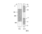
図14(A)は、ゲート電極に配線接続用のコンタクトパッド部が設けられた比較例のトランジスターT10を示す平面図である。トランジスターT10は、図14(A)に示すように、ゲート電極G10と、ドレイン領域AD10と、ソース領域AS10と、を備えている。
ゲート電極G10には、チャネル領域AC10より外側に突出するコンタクトパッド部GP10が設けられている。このようなトランジスターT10では、配線と接続するためのコンタクトホールH10は、コンタクトパッド部GP10上に設けられる。言い換えると、コンタクトホールH10は、チャネル領域AC10と平面視において重ならない位置に設けられる。
FIG. 14A is a plan view showing a transistor T10 of a comparative example in which a contact pad portion for wiring connection is provided on the gate electrode. As illustrated in FIG. 14A, the transistor T10 includes a gate electrode G10, a drain region AD10, and a source region AS10.
The gate electrode G10 is provided with a contact pad portion GP10 that protrudes outward from the channel region AC10. In such a transistor T10, the contact hole H10 for connecting to the wiring is provided on the contact pad portion GP10. In other words, the contact hole H10 is provided at a position that does not overlap with the channel region AC10 in plan view.
トランジスターT10では、コンタクトパッド部GP10が設けられているため、ゲート電極G10の大きさは、チャネル領域AC10に比べて大きくなり、その結果、トランジスター全体の幅が大きくなってしまうという問題があった。そのため、複数のトランジスターを配置して構成される画素回路の小型化には限界があった。 In the transistor T10, since the contact pad portion GP10 is provided, the size of the gate electrode G10 is larger than that of the channel region AC10. As a result, there is a problem that the width of the entire transistor is increased. For this reason, there is a limit to downsizing a pixel circuit configured by arranging a plurality of transistors.
一方、図14(B)は、本実施形態のトランジスターT5を示す平面図である。トランジスターT5は、図14(B)に示すように、ゲート電極G5と、ドレイン領域AD5と、ソース領域AS5と、を備えている。
上記の問題に対して、本実施形態のトランジスターT5によれば、ゲート電極G5と配線とが、チャネル領域AC5と平面視で重なる位置において接続される。言い換えると、ゲート電極G5と配線とを接続するコンタクトホールH5がチャネル領域AC5と平面視で重なる位置に設けられる。そのため、ゲート電極G5に配線接続用のコンタクトパッド部を設ける必要がなく、ゲート電極G5の平面視における大きさをチャネル領域AC5とほぼ同じ大きさにすることができる。これにより、図14(A),(B)に示すように、比較例のトランジスターT10に比べて、本実施形態のトランジスターT5においては、幅方向(X方向)の長さを小さくできる。したがって、本実施形態によれば、画素回路をより小型化できる発光装置が得られる。
On the other hand, FIG. 14B is a plan view showing the transistor T5 of this embodiment. As shown in FIG. 14B, the transistor T5 includes a gate electrode G5, a drain region AD5, and a source region AS5.
With respect to the above problem, according to the transistor T5 of the present embodiment, the gate electrode G5 and the wiring are connected at a position overlapping the channel region AC5 in plan view. In other words, the contact hole H5 connecting the gate electrode G5 and the wiring is provided at a position overlapping the channel region AC5 in plan view. Therefore, it is not necessary to provide a contact pad portion for wiring connection on the gate electrode G5, and the size of the gate electrode G5 in plan view can be made substantially the same as that of the channel region AC5. Thereby, as shown in FIGS. 14A and 14B, the length in the width direction (X direction) can be made smaller in the transistor T5 of this embodiment than in the transistor T10 of the comparative example. Therefore, according to the present embodiment, a light emitting device capable of further downsizing the pixel circuit can be obtained.
本実施形態の効果について、さらに図3を参照しつつ具体的に説明する。
本実施形態によれば、図3に示す駆動トランジスターTDR及びリセットトランジスターT4と、選択トランジスターT1、発光制御トランジスターT2、及び補償トランジスターT3との距離、すなわち、仮想直線K1と仮想直線K2との距離D1を、コンタクトホールがチャネル領域と平面視で重ならない位置に設けられる場合に比べて、小さくすることができる。また、信号線26及び第3電源導電体27をより各トランジスターに近い位置に形成することができる。したがって、本実施形態によれば、画素回路P11の幅(X方向長さ)D2をより小さくでき、画素回路を小型化できる。
The effect of the present embodiment will be specifically described with reference to FIG.
According to the present embodiment, the distance between the drive transistor TDR and reset transistor T4 shown in FIG. 3, the selection transistor T1, the light emission control transistor T2, and the compensation transistor T3, that is, the distance D1 between the virtual straight line K1 and the virtual straight line K2. Can be made smaller than when the contact hole is provided at a position not overlapping the channel region in plan view. In addition, the
また、本実施形態によれば、画素回路P11には、駆動トランジスターTDRの閾値電圧のばらつきに起因した発光素子45への供給電流のばらつきを補償するための補償回路が組み込まれている。そのため、諧調レベルに応じた電流を発光素子45に安定して供給できる。これにより、チャネルと平面視で重なる位置において、ゲート電極と配線とが接続されるコンタクトが形成されることによって、駆動トランジスターTDRの閾値電圧がばらついてしまうような場合であっても、発光素子45の輝度がばらつくことを抑制できる。
Further, according to the present embodiment, the pixel circuit P11 incorporates a compensation circuit for compensating for the variation in the supply current to the
また、トランジスターのチャネル領域においては、ソース領域とドレイン領域とのうち電位が高い側の領域に近い方がゲート電極によって生じる電界が小さい。これは、電位が高い側の領域とゲート電極との間の電圧の方が、電位が低い側の領域とゲート電極との間の電圧よりも大きくなるためである。これにより、ゲート電極と配線とを接続するコンタクトホールを、ソース領域とドレイン領域とのうち電位が高い側の領域に近く、すなわち、電界の影響が小さい位置に設けることで、チャネル領域と平面視で重なる位置にコンタクトホールを設けた場合であっても、トランジスターの閾値電圧のばらつきに与える影響を小さくできる。 In the channel region of the transistor, the electric field generated by the gate electrode is smaller in the region closer to the higher potential region of the source region and the drain region. This is because the voltage between the higher potential region and the gate electrode is larger than the voltage between the lower potential region and the gate electrode. As a result, the contact hole for connecting the gate electrode and the wiring is provided close to the higher potential region of the source region and the drain region, that is, at a position where the influence of the electric field is small, so that Even when contact holes are provided at overlapping positions, the influence on variations in threshold voltage of transistors can be reduced.
図15(A)は、Pチャネル型のトランジスターにおけるコンタクトホールの設置位置を示す平面図である。図15(B)は、Nチャネル型のトランジスターにおけるコンタクトホールの設置位置を示す平面図である。
図15(A)に示すように、Pチャネル型のトランジスターにおいて、チャネル領域ACと平面視で重なる位置におけるゲート電極G上にコンタクトホールHを設ける場合には、コンタクトホールHは、ソース領域AS寄りに設けることが好ましい。Pチャネル型のトランジスターにおいては、キャリアが正孔となるため、ソース領域ASが高電位側となり、ドレイン領域ADが低電位側となるためである。
FIG. 15A is a plan view showing a contact hole installation position in a P-channel transistor. FIG. 15B is a plan view showing a contact hole installation position in an N-channel transistor.
As shown in FIG. 15A, in a P-channel transistor, when a contact hole H is provided on the gate electrode G at a position overlapping the channel region AC in plan view, the contact hole H is closer to the source region AS. It is preferable to provide in. This is because in the P-channel transistor, carriers are holes, so that the source region AS is on the high potential side and the drain region AD is on the low potential side.
一方、図15(B)に示すように、Nチャネル型のトランジスターにおいて、チャネル領域ACと平面視で重なる位置におけるゲート電極G上にコンタクトホールHを設ける場合には、コンタクトホールHは、ドレイン領域AD寄りに設けることが好ましい。Nチャネル型のトランジスターにおいては、キャリアが電子となるため、ドレイン領域ADが高電位側となり、ソース領域ASが低電位側となるためである。 On the other hand, as shown in FIG. 15B, in the N-channel transistor, when the contact hole H is provided over the gate electrode G at a position overlapping the channel region AC in plan view, the contact hole H is formed in the drain region. It is preferable to provide it close to AD. This is because in the N-channel transistor, carriers are electrons, so that the drain region AD is on the high potential side and the source region AS is on the low potential side.
本実施形態によれば、図3に示すように、選択トランジスターT1、発光制御トランジスターT2、補償トランジスターT3、及びリセットトランジスターT4におけるゲート電極と各配線との接続位置は、ゲート電極上におけるソース領域寄りとなっている。
本実施形態においては、トランジスターがPチャネル型であるため、ソース領域寄りにコンタクトホールを設けることでトランジスターの閾値電圧のばらつきを抑制できる。
According to the present embodiment, as shown in FIG. 3, the connection position between the gate electrode and each wiring in the selection transistor T1, the light emission control transistor T2, the compensation transistor T3, and the reset transistor T4 is close to the source region on the gate electrode. It has become.
In this embodiment, since the transistor is a P-channel type, variation in threshold voltage of the transistor can be suppressed by providing a contact hole near the source region.
また、本実施形態においては、図13(B),(C)に示すように、絶縁層LAの上面LAaからドレイン領域AD及びソース領域ASまでの深さDSと、絶縁層LAの上面LAaからゲート電極Gまでの深さDGとは異なる。具体的には、絶縁層LAの上面LAaからドレイン領域AD及びソース領域ASまでの深さDSは、絶縁層LAの上面LAaからゲート電極Gまでの深さDGよりも大きい。そのため、仮にドレイン領域AD及びソース領域ASのコンタクトホールHS,HSと、ゲート電極GのコンタクトホールHGと、を一度のエッチングで形成したとすると、ゲート電極Gにダメージが生じる虞があった。 In this embodiment, as shown in FIGS. 13B and 13C, the depth DS from the upper surface LAa of the insulating layer LA to the drain region AD and the source region AS, and the upper surface LAa of the insulating layer LA. This is different from the depth DG to the gate electrode G. Specifically, the depth DS from the upper surface LAa of the insulating layer LA to the drain region AD and the source region AS is larger than the depth DG from the upper surface LAa of the insulating layer LA to the gate electrode G. For this reason, if the contact holes HS and HS of the drain region AD and the source region AS and the contact hole HG of the gate electrode G are formed by one etching, the gate electrode G may be damaged.
これに対して、本実施形態によれば、ドレイン領域AD及びソース領域ASのコンタクトホールと、ゲート電極Gのコンタクトホールとは、別工程で形成される。そのため、それぞれの形成するコンタクトホールの深さに応じたエッチング方法を選択でき、ゲート電極Gにダメージが生じることを抑制できる。 On the other hand, according to the present embodiment, the contact hole of the drain region AD and the source region AS and the contact hole of the gate electrode G are formed in separate steps. Therefore, an etching method corresponding to the depth of each contact hole to be formed can be selected, and damage to the gate electrode G can be suppressed.
また、本実施形態によれば、トランジスターと接続される各配線は、トランジスター上に積層された多層配線層に設けられているため、配線をトランジスターと平面視で重なるように配置することができ、画素回路を小型化できる。また、これにより、本実施形態によれば、チャネル領域と平面視で重なる位置にコンタクトホールを形成することが容易である。 In addition, according to the present embodiment, each wiring connected to the transistor is provided in a multilayer wiring layer stacked on the transistor, so that the wiring can be arranged so as to overlap with the transistor in plan view. The pixel circuit can be downsized. Accordingly, according to the present embodiment, it is easy to form a contact hole at a position overlapping the channel region in plan view.
なお、本実施形態においては、以下の構成を採用することもできる。 In the present embodiment, the following configuration may be employed.
上記説明した実施形態においては、画素回路P11に含まれるすべてのトランジスターが、チャネル領域と平面視において重なる位置において、ゲート電極と各配線とが接続されている構成としたが、これに限られない。
本実施形態においては、例えば、図16に示す画素回路P12のように、一部のトランジスターのみにおいて、チャネル領域と平面視において重なる位置で、ゲート電極と配線とが接続されている構成としてもよい。
In the above-described embodiment, the configuration is such that all the transistors included in the pixel circuit P11 are connected to the gate electrode and each wiring at a position overlapping the channel region in plan view. .
In the present embodiment, for example, as in the pixel circuit P12 illustrated in FIG. 16, only a part of the transistors may have a configuration in which the gate electrode and the wiring are connected at a position overlapping the channel region in plan view. .
図16に示す画素回路P12においては、選択トランジスターT1、発光制御トランジスターT2、及び補償トランジスターT3において、チャネル領域と平面視で重なる位置で、ゲート電極と配線とが接続されている。一方、駆動トランジスターTDRaにおいては、ゲート電極GDRaにコンタクトパッド部GP11が設けられ、コンタクトパッド部GP11にコンタクトホールHA8が設けられている。リセットトランジスターT4aにおいては、ゲート電極G4aにコンタクトパッド部GP12が設けられ、コンタクトパッド部GP12にコンタクトホールH4が設けられている。 In the pixel circuit P12 shown in FIG. 16, in the selection transistor T1, the light emission control transistor T2, and the compensation transistor T3, the gate electrode and the wiring are connected at a position overlapping the channel region in plan view. On the other hand, in the driving transistor TDRa, the contact pad portion GP11 is provided in the gate electrode GDRa, and the contact hole HA8 is provided in the contact pad portion GP11. In the reset transistor T4a, a contact pad part GP12 is provided in the gate electrode G4a, and a contact hole H4 is provided in the contact pad part GP12.
本実施形態のように、5つのトランジスターを2列に並べて配置するような場合においては、いずれか一方の列に設けられたトランジスターにおいて、チャネル領域と平面視で重なる位置で、ゲート電極と配線とを接続することにより、その列の幅を小さくできるため、画素回路P12の幅D3を小さくすることができる。本実施形態においては、選択トランジスターT1、発光制御トランジスターT2、及び補償トランジスターT3からなる列、すなわち、仮想直線K2に沿うトランジスターの列の幅を小さくすることができる。 In the case where five transistors are arranged in two rows as in this embodiment, in the transistors provided in any one row, the gate electrode and the wiring are arranged at a position overlapping the channel region in plan view. Since the width of the column can be reduced by connecting, the width D3 of the pixel circuit P12 can be reduced. In this embodiment, it is possible to reduce the width of the row of the selection transistor T1, the light emission control transistor T2, and the compensation transistor T3, that is, the row of transistors along the virtual straight line K2.
また、本実施形態においては、駆動トランジスター及びリセットトランジスターにおいて、チャネル領域と平面視で重なる位置で、ゲート電極と配線とが接続され、選択トランジスター、発光制御トランジスター、及び補償トランジスターにおいて、コンタクトパッド部においてゲート電極と配線とが接続されているような構成としてもよい。この場合においては、駆動トランジスター及びリセットトランジスターからなる列、すなわち仮想直線K1に沿うトランジスターの列の幅を小さくできるため、画素回路の幅を小さくすることができる。 In the present embodiment, in the driving transistor and the reset transistor, the gate electrode and the wiring are connected at a position overlapping the channel region in plan view. In the selection transistor, the light emission control transistor, and the compensation transistor, in the contact pad portion A configuration in which the gate electrode and the wiring are connected may be employed. In this case, the width of the pixel circuit can be reduced because the width of the row of transistors including the drive transistor and the reset transistor, that is, the row of transistors along the virtual line K1, can be reduced.
(第2実施形態)
第2実施形態は、第1実施形態に比べて、補償トランジスター及びリセットトランジスターが設けられていない点において異なる。
なお、上記実施形態と同様の構成については、適宜同一の符号を付す等によって説明を省略する場合がある。
(Second Embodiment)
The second embodiment is different from the first embodiment in that a compensation transistor and a reset transistor are not provided.
In addition, about the structure similar to the said embodiment, description may be abbreviate | omitted by attaching | subjecting the same code | symbol suitably.
図17は、本実施形態の画素回路P21を示す回路図である。図18及び図19は、本実施形態の画素回路P21を模式的に示す平面図である。図18においては、配線及びコンタクトホールの図示を省略している。 FIG. 17 is a circuit diagram showing the pixel circuit P21 of the present embodiment. 18 and 19 are plan views schematically showing the pixel circuit P21 of the present embodiment. In FIG. 18, illustration of wiring and contact holes is omitted.
本実施形態の画素回路P21は、図17に示すように、駆動トランジスター(第1トランジスター)TDR1と、選択トランジスターT11と、発光制御トランジスターT2と、容量素子Cと、を備える。
駆動トランジスターTDR1及び選択トランジスターT11は、第1実施形態の駆動トランジスターTDR及び選択トランジスターT1と同様の機能を有する。
As illustrated in FIG. 17, the pixel circuit P <b> 21 of the present embodiment includes a drive transistor (first transistor) TDR <b> 1, a selection transistor T <b> 11, a light emission control transistor T <b> 2, and a capacitive element C.
The driving transistor TDR1 and the selection transistor T11 have the same functions as the driving transistor TDR and the selection transistor T1 of the first embodiment.
駆動トランジスターTDR1は、ソースが第1電源導電体41に接続され、ドレインが発光制御トランジスターT2のソースと接続され、ゲートが、選択トランジスターのドレイン及び容量素子Cの第1電極C1と接続されている。
選択トランジスターT11は、ソースが信号線26に接続され、ドレインが駆動トランジスターTDR1のゲート及び容量素子Cの第1電極C1と接続されている。
The drive transistor TDR1 has a source connected to the first
The selection transistor T11 has a source connected to the
発光制御トランジスターT2は、駆動トランジスターTDR1と発光素子45との間に設けられている。発光制御トランジスターT2は、ソースが駆動トランジスターTDR1のドレインに接続され、ドレインが発光素子45の画素電極451に接続され、ゲートが制御線24に接続されている。
The light emission control transistor T2 is provided between the drive transistor TDR1 and the
本実施形態においては、図18に示すように、各トランジスターTDR1,T11,T2は、Y方向に延在する素子部EDR1,E11,E2と、ゲート電極GDR1,G11,G2と、を備えている。駆動トランジスターTDR1の素子部EDR1、選択トランジスターT11の素子部E11、及び発光制御トランジスターT2の素子部E2は、それぞれ、長さ方向がY方向となるように配置されている。 In the present embodiment, as shown in FIG. 18, each of the transistors TDR1, T11, T2 includes element portions EDR1, E11, E2 extending in the Y direction, and gate electrodes GDR1, G11, G2. . The element portion EDR1 of the driving transistor TDR1, the element portion E11 of the selection transistor T11, and the element portion E2 of the light emission control transistor T2 are arranged so that the length direction is the Y direction.
選択トランジスターT11及び発光制御トランジスターT2は、駆動トランジスターTDR1の一方側(+X側)に長さ方向(Y方向)に並んで設けられている。すなわち、駆動トランジスターTDR1と、選択トランジスターT11及び発光制御トランジスターT2と、は2列になるように配置されている。 The selection transistor T11 and the light emission control transistor T2 are provided side by side in the length direction (Y direction) on one side (+ X side) of the drive transistor TDR1. That is, the drive transistor TDR1, the selection transistor T11, and the light emission control transistor T2 are arranged in two rows.
駆動トランジスターTDR1のゲート電極GDR1は、選択トランジスターT11側(+X側)に突出するコンタクトパッド部GP21を有している。コンタクトパッド部GP21は、平面視において、駆動トランジスターTDR1のチャネル領域ACDR1と重ならない位置に設けられている。 The gate electrode GDR1 of the driving transistor TDR1 has a contact pad portion GP21 that protrudes to the selection transistor T11 side (+ X side). The contact pad portion GP21 is provided at a position that does not overlap with the channel region ACDR1 of the drive transistor TDR1 in plan view.
選択トランジスターT11は、駆動トランジスターTDR1側(−X側)に突出するコンタクトパッド部GP22を有している。コンタクトパッド部GP22は、平面視において、選択トランジスターT11のチャネル領域AC11と重ならない位置に設けられている。 The selection transistor T11 has a contact pad portion GP22 that protrudes toward the driving transistor TDR1 (−X side). The contact pad portion GP22 is provided at a position that does not overlap with the channel region AC11 of the selection transistor T11 in plan view.
図18及び図19に示すように、駆動トランジスターTDR1のゲート電極GDR1は、コンタクトパッド部GP21において、コンタクトホールH21を介して、中継電極(配線)Q21と接続されている。選択トランジスターT11のゲート電極G11は、コンタクトパッド部GP22において、コンタクトホールH22を介して、走査線22と接続されている。発光制御トランジスターT2は、チャネル領域AC2と平面視で重なる位置において、ゲート電極G2が制御線24と、コンタクトホールH23を介して接続されている。
As shown in FIGS. 18 and 19, the gate electrode GDR1 of the drive transistor TDR1 is connected to the relay electrode (wiring) Q21 via the contact hole H21 in the contact pad portion GP21. The gate electrode G11 of the selection transistor T11 is connected to the
本実施形態によれば、発光制御トランジスターT2において、チャネル領域AC2と平面視において重なる位置で、ゲート電極G2と制御線24とが接続されているため、第1実施形態と同様にして、画素回路P21をより小型化することができる。
According to the present embodiment, in the light emission control transistor T2, since the gate electrode G2 and the
なお、本実施形態においては、駆動トランジスターTDR1と選択トランジスターT11とのうち、いずれか一方、もしくは両方において、チャネル領域と平面視において重なる位置で、ゲート電極が各配線と接続される構成としてもよい。 In the present embodiment, the gate electrode may be connected to each wiring at a position overlapping with the channel region in a plan view in one or both of the driving transistor TDR1 and the selection transistor T11. .
(第3実施形態)
第3実施形態は、第1実施形態に対して、リセットトランジスターが設けられていない点において異なる。
なお、上記実施形態と同様の構成については、適宜同一の符号を付す等によって説明を省略する場合がある。
(Third embodiment)
The third embodiment is different from the first embodiment in that no reset transistor is provided.
In addition, about the structure similar to the said embodiment, description may be abbreviate | omitted by attaching | subjecting the same code | symbol suitably.
図20は、本実施形態の画素回路P31を示す回路図である。図21及び図22は、本実施形態の画素回路P31を模式的に示す平面図である。図21においては、配線及びコンタクトホールの図示を省略している。 FIG. 20 is a circuit diagram showing the pixel circuit P31 of the present embodiment. 21 and 22 are plan views schematically showing the pixel circuit P31 of the present embodiment. In FIG. 21, illustration of wiring and contact holes is omitted.
本実施形態の画素回路P31は、図20に示すように、駆動トランジスターTDRと、選択トランジスターT12と、発光制御トランジスターT2と、補償トランジスターT32と、容量素子Cと、を備える。
選択トランジスターT12及び補償トランジスターT32は、第1実施形態の選択トランジスターT1及び補償トランジスターT3と同様の機能を有する。
As shown in FIG. 20, the pixel circuit P31 of the present embodiment includes a drive transistor TDR, a selection transistor T12, a light emission control transistor T2, a compensation transistor T32, and a capacitive element C.
The selection transistor T12 and the compensation transistor T32 have the same functions as the selection transistor T1 and the compensation transistor T3 of the first embodiment.
各トランジスターの接続は、リセットトランジスターが設けられていない点を除いて、第1実施形態において図2に示した回路図と同様である。 The connection of each transistor is the same as that of the circuit diagram shown in FIG. 2 in the first embodiment except that the reset transistor is not provided.
本実施形態においては、図21に示すように、各トランジスターTDR,T12,T2,T32は、Y方向に延在する素子部EDR,E12,E2,E32と、ゲート電極GDR,G12,G2,G32と、を備えている。駆動トランジスターTDRの素子部EDR、選択トランジスターT12の素子部E12、発光制御トランジスターT2の素子部E2、及び補償トランジスターT32の素子部E32は、それぞれ、長さ方向がY方向となるように配置されている。 In the present embodiment, as shown in FIG. 21, each of the transistors TDR, T12, T2, and T32 includes element portions EDR, E12, E2, and E32 extending in the Y direction and gate electrodes GDR, G12, G2, and G32. And. The element portion EDR of the driving transistor TDR, the element portion E12 of the selection transistor T12, the element portion E2 of the light emission control transistor T2, and the element portion E32 of the compensation transistor T32 are arranged so that the length direction is the Y direction. Yes.
選択トランジスターT12及び補償トランジスターT32は、駆動トランジスターTDRの一方側(+X側)に長さ方向(Y方向)に並んで設けられている。すなわち、駆動トランジスターTDR1と、選択トランジスターT11及び発光制御トランジスターT2と、は2列になるように配置されている。 The selection transistor T12 and the compensation transistor T32 are provided side by side in the length direction (Y direction) on one side (+ X side) of the drive transistor TDR. That is, the drive transistor TDR1, the selection transistor T11, and the light emission control transistor T2 are arranged in two rows.
発光制御トランジスターT2は、駆動トランジスターTDR、選択トランジスターT12、及び補償トランジスターT32よりも図示上側(−Y側)に設けられており、幅方向(X方向)において、駆動トランジスターTDRと、選択トランジスターT12及び補償トランジスターT32との間に設けられている。 The light emission control transistor T2 is provided on the upper side (−Y side) of the driving transistor TDR, the selection transistor T12, and the compensation transistor T32, and in the width direction (X direction), the driving transistor TDR, the selection transistor T12, and It is provided between the compensation transistor T32.
図21及び図22に示すように、駆動トランジスターTDRのゲート電極GDRは、チャネル領域ACDRと平面視で重なる位置において、ゲート電極GDRが中継電極(配線)Q31と、コンタクトホールH31を介して接続されている。選択トランジスターT12は、チャネル領域AC12と平面視で重なる位置において、ゲート電極G12が走査線22と、コンタクトホールH32を介して接続されている。発光制御トランジスターT2は、チャネル領域AC2と平面視で重なる位置において、ゲート電極G2が制御線24と、コンタクトホールH33を介して接続されている。補償トランジスターT32は、チャネル領域AC32と平面視で重なる位置において、ゲート電極G32が制御線23と、コンタクトホールH34を介して接続されている。
As shown in FIGS. 21 and 22, the gate electrode GDR of the driving transistor TDR is connected to the relay electrode (wiring) Q31 via the contact hole H31 at a position overlapping the channel region ADDR in plan view. ing. In the selection transistor T12, the gate electrode G12 is connected to the
本実施形態によれば、各トランジスターにおいて、チャネル領域と平面視において重なる位置で、ゲート電極と各配線とが接続されているため、第1実施形態と同様にして、画素回路P31の幅D4をより小さくすることができる。 According to the present embodiment, in each transistor, since the gate electrode and each wiring are connected at a position overlapping the channel region in plan view, the width D4 of the pixel circuit P31 is set as in the first embodiment. It can be made smaller.
なお、本実施形態においては、各トランジスターの一部において、ゲート電極に配線接続用のコンタクトパッド部が設けられる構成としてもよい。言い換えると、本実施形態においては、各トランジスターの一部において、チャネル領域と平面視で重ならない位置で、ゲート電極が各配線と接続される構成としてもよい。 In the present embodiment, a contact pad portion for wiring connection may be provided on the gate electrode in a part of each transistor. In other words, in this embodiment, the gate electrode may be connected to each wiring at a position that does not overlap with the channel region in plan view in a part of each transistor.
[電子機器]
上述の各実施形態に例示した発光装置100は、各種の電子機器の表示装置として好適に利用される。
図23は、電子機器の一例として、第1実施形態の発光装置100を利用した頭部装着型の表示装置90(HMD:Head Mounted Display)を示す概略構成図である。
[Electronics]
The
FIG. 23 is a schematic configuration diagram showing a head-mounted display device 90 (HMD: Head Mounted Display) using the
表示装置90は、人間の頭部に装着可能な電子機器であり、使用者の左眼に重なる透過部(レンズ)92Lと、使用者の右眼に重なる透過部92Lと、左眼用の発光装置100L及びハーフミラー94Lと、右眼用の発光装置100R及びハーフミラー94Rと、を備える。発光装置100Lと発光装置100Rとは、射出光が相互に反対の方向に進行するように配置される。左眼用のハーフミラー94Lは、透過部92Lの透過光を使用者の左眼側に透過させるとともに、発光装置100Lからの射出光を使用者の左眼側に反射させる。同様に、右眼用のハーフミラー94Rは、透過部92Rの透過光を使用者の右眼側に透過させるとともに、発光装置100Rからの射出光を使用者の右眼側に反射させる。
The
したがって、使用者は、透過部92L及び透過部92Rを介して観察される像と、各発光装置100L,100Rによる表示画像と、を重畳した画像を知覚する。また、相互に視差が付与された立体視画像(左眼用画像および右眼用画像)を発光装置100Lと発光装置100Rとに表示させることで、使用者に表示画像の立体感を知覚させることが可能である。
Therefore, the user perceives an image obtained by superimposing an image observed through the
なお、各実施形態の発光装置が適用される電子機器は、図23の表示装置90に限定されない。例えば、ビデオカメラやスチルカメラ等の撮像装置に利用される電子式ビューファインダー(EVF:Electronic View Finder)にも本実施形態の発光装置が好適に利用される。また、携帯電話機、携帯情報端末(スマートフォン)、テレビやパーソナルコンピューター等のモニター、カーナビゲーション装置等の各種の電子機器に本実施形態の発光装置を採用することが可能である。
Note that the electronic apparatus to which the light-emitting device of each embodiment is applied is not limited to the
また、上記説明した電子機器の例では、発光装置として第1実施形態の発光装置100を用いたが、これに限られず、第2実施形態及び第3実施形態のいずれかの発光装置を用いてもよいことは言うまでもない。
In the example of the electronic apparatus described above, the
第1実施形態から第3実施形態におけるトランジスターにおいて、チャネル領域はゲート電極と同一の領域に形成され、所謂セルフアライン構造であった。しかしながら、ソース領域又は/及びドレイン領域の一部がゲート電極と重なるように構成してもよいし、ゲート電極とソース領域又は/及びドレイン領域との間にスペースがあってもよい。 In the transistors according to the first to third embodiments, the channel region is formed in the same region as the gate electrode, and has a so-called self-aligned structure. However, a part of the source region or / and the drain region may overlap with the gate electrode, or there may be a space between the gate electrode and the source region or / and the drain region.
第1実施形態から第3実施形態におけるトランジスターは、ソース領域と、ゲート電極と、ドレイン領域と、チャネル領域とを有していた。このソース領域又は/及びドレイン領域を低不純物濃度領域と高不純物領域の2種類の不純物領域で構成してもよい。すなわち、第1実施形態から第3実施形態におけるトランジスターは、LDD(Lightly Doped Drain)構造を有してもよい。LDD構造により、ホットキャリアの発生を抑えることができる。さらに、低不純物濃度領域がゲート電極と平面視重なるように構成してもよい。 The transistor in the first to third embodiments has a source region, a gate electrode, a drain region, and a channel region. This source region and / or drain region may be composed of two types of impurity regions, a low impurity concentration region and a high impurity region. That is, the transistors in the first to third embodiments may have an LDD (Lightly Doped Drain) structure. With the LDD structure, generation of hot carriers can be suppressed. Furthermore, the low impurity concentration region may be configured to overlap the gate electrode in plan view.
ここで、複数のトランジスターのうち少なくとも一つは、ソース領域又は/及びドレイン領域の少なくとも一部と平面視で重なる位置において、ゲート電極に配線が接続されていてもよい。 Here, at least one of the plurality of transistors may have a wiring connected to the gate electrode at a position overlapping at least part of the source region and / or the drain region in plan view.
第1実施形態の画素回路P11や第3実施形態の画素回路P31は、特開2013−088611号公報の図13乃至図17及びその説明に示す駆動方法のように動作させてもよいし、適宜変形可能である。 The pixel circuit P11 of the first embodiment and the pixel circuit P31 of the third embodiment may be operated as in the driving method shown in FIGS. 13 to 17 of JP 2013-088611 A and the description thereof, or as appropriate. It can be deformed.
また、第1実施形態の画素回路P11や第3実施形態の画素回路P31を所謂電流プログラム方式で駆動してもよい。この場合、信号線26に接続した容量素子Cpは省略される。図20の選択トランジスターT12及び補償トランジスターT32をオン状態、発光制御トランジスターT2をオフ状態とし、階調レベルに応じた信号電流を信号線26に流して、駆動トランジスターTDRのソース−ゲート間電圧を信号電流に応じた電圧にしてプログラミングを行い、図20の選択トランジスターT12及び補償トランジスターT32をオフ状態、発光制御トランジスターT2をオン状態として、駆動トランジスターTDRのソース−ゲート間電圧に応じた電流を駆動トランジスターTDRから発光素子45に供給するようにしてもよい。
Further, the pixel circuit P11 of the first embodiment and the pixel circuit P31 of the third embodiment may be driven by a so-called current program method. In this case, the capacitive element Cp connected to the
また、図17の画素回路P21は、特開2013−088611号公報の図4乃至図10及びその説明に示す駆動方法のように動作させてもよい。 In addition, the pixel circuit P21 in FIG. 17 may be operated as in the driving method illustrated in FIGS. 4 to 10 and the description thereof in JP2013-088611A.
また、上記第1実施形態から第3実施形態の発光装置における各種電極、配線、トランジスター、容量素子、絶縁膜等の構成材料、形状、配置、寸法や膜厚等の具体的な記載は一例に過ぎず、適宜変更が可能である。 In addition, specific descriptions of constituent materials, shapes, arrangements, dimensions, film thicknesses, and the like of various electrodes, wirings, transistors, capacitors, insulating films, and the like in the light emitting devices of the first to third embodiments are given as an example. However, it can be changed as appropriate.
22…走査線(配線)、23,24,25…制御線(配線)、26…信号線、90…表示装置(電子機器)、100,100L,100R…発光装置、AC,AC1,AC2,AC3,AC4,AC10,AC11,AC12,AC32,ACDR,ACDR1…チャネル領域、G,G1,G2,G3,G4,G4a,G10,G11,G12,G32,GDR,GDR1,GDRa…ゲート電極、P,P11,P12,P21,P31…画素回路、Q21,Q31,QA3…中継電極(配線)、T1,T11,T12…選択トランジスター、T2…発光制御トランジスター(第2トランジスター)、T3,T32…補償トランジスター、T4,T4a…リセットトランジスター、TDR,TDR1…駆動トランジスター(第1トランジスター) 22 ... Scanning line (wiring), 23,24,25 ... Control line (wiring), 26 ... Signal line, 90 ... Display device (electronic device), 100, 100L, 100R ... Light emitting device, AC, AC1, AC2, AC3 , AC4, AC10, AC11, AC12, AC32, ACDR, ACDR1 ... channel region, G, G1, G2, G3, G4, G4a, G10, G11, G12, G32, GDR, GDR1, GDRa ... gate electrodes, P, P11 , P12, P21, P31 ... Pixel circuit, Q21, Q31, QA3 ... Relay electrode (wiring), T1, T11, T12 ... Selection transistor, T2 ... Light emission control transistor (second transistor), T3, T32 ... Compensation transistor, T4 , T4a ... reset transistor, TDR, TDR1 ... drive transistor (first transistor )
Claims (15)
前記第1トランジスターのゲート電極には、チャネル領域と平面視で重ならない位置において配線が接続された第1コンタクトパッド部が設けられ、
前記複数のトランジスターは、前記第1方向と直交する第2方向において前記第1トランジスターの一方側に配置された複数のトランジスターを含むトランジスター群を含み、
前記トランジスター群に含まれたトランジスターは、前記第1方向に並んで設けられ、
前記トランジスター群は、
チャネル領域と平面視で重なる位置において、ゲート電極に配線が接続されているトランジスターと、
ゲート電極に、チャネル領域と平面視で重ならない位置において配線が接続されている第2コンタクトパッド部が設けられたトランジスターと、
を含み、
前記第1コンタクトパッド部は、前記第2方向において前記トランジスター群側に突出し、
前記第2コンタクトパッド部は、前記第2方向において前記第1トランジスター側に突出し、
前記第1コンタクトパッド部と前記第2コンタクトパッド部とは、前記第1方向に並んで配置されていることを特徴とする発光装置。 A pixel circuit comprising: a plurality of transistors including a first transistor having an element portion extending in a first direction; and a light emitting element to which current is supplied by the first transistor;
The gate electrode of the first transistor is provided with a first contact pad portion to which wiring is connected at a position not overlapping the channel region in plan view,
Wherein the plurality of transistors over includes a transistor group including a plurality of transistors which are arranged on one side of the first transistor in the second direction perpendicular to the first direction,
The transistors included in the transistor group are provided side by side in the first direction,
The transistor group is:
A transistor whose wiring is connected to the gate electrode at a position overlapping the channel region in plan view ;
A transistor provided with a second contact pad portion to which a wiring is connected to the gate electrode at a position not overlapping the channel region in plan view;
Including
The first contact pad portion protrudes toward the transistor group in the second direction;
The second contact pad portion protrudes toward the first transistor in the second direction;
The light emitting device, wherein the first contact pad portion and the second contact pad portion are arranged side by side in the first direction .
前記選択トランジスターは、チャネル領域と平面視で重なる位置において、ゲート電極に配線が接続されている、請求項1に記載の発光装置。 The plurality of transistors include a selection transistor provided between a gate of the first transistor and a signal line for inputting a signal to the gate of the first transistor,
The light emitting device according to claim 1, wherein the selection transistor has a wiring connected to the gate electrode at a position overlapping the channel region in plan view.
前記補償トランジスターは、チャネル領域と平面視で重なる位置において、ゲート電極に配線が接続されている、請求項1または2に記載の発光装置。 The plurality of transistors include a compensation transistor provided between a gate of the first transistor and one current terminal of the first transistor,
The light emitting device according to claim 1, wherein the compensation transistor has a wiring connected to a gate electrode at a position overlapping the channel region in plan view.
前記発光制御トランジスターは、チャネル領域と平面視で重なる位置において、ゲート電極に配線が接続されている、請求項1から3のいずれか一項に記載の発光装置。 The plurality of transistors include a light emission control transistor provided between the first transistor and the light emitting element,
4. The light emitting device according to claim 1, wherein the light emission control transistor has a wiring connected to a gate electrode at a position overlapping the channel region in plan view.
前記リセットトランジスターは、チャネル領域と平面視で重なる位置において、ゲート電極に配線が接続されている、請求項1から4のいずれか一項に記載の発光装置。 The plurality of transistors include a reset transistor that supplies a predetermined reset potential to the light emitting element,
5. The light-emitting device according to claim 1, wherein the reset transistor has a wiring connected to a gate electrode at a position overlapping the channel region in plan view.
前記第1トランジスターのゲート電極には、チャネル領域と平面視で重ならない位置において配線が接続された第1コンタクトパッド部が設けられ、
前記複数のトランジスターは、前記第1方向と直交する第2方向において前記第1トランジスターの一方側に配置された複数のトランジスターを含むトランジスター群を含み、
前記トランジスター群に含まれたトランジスターは、前記第1方向に並んで設けられ、
前記トランジスター群は、
チャネル領域と平面視で重なる位置において、ゲート電極に配線が接続されている第2トランジスターと、
ゲート電極に、チャネル領域と平面視で重ならない位置において配線が接続されている第2コンタクトパッド部が設けられたトランジスターと、
を含み、
前記第1コンタクトパッド部は、前記第2方向において前記トランジスター群側に突出し、
前記第2コンタクトパッド部は、前記第2方向において前記第1トランジスター側に突出し、
前記第1コンタクトパッド部と前記第2コンタクトパッド部とは、前記第1方向に並んで配置され、
前記第2トランジスターは、前記第1トランジスターと前記発光素子との間に設けられていることを特徴とする発光装置。 A pixel circuit comprising: a plurality of transistors including a first transistor having an element portion extending in a first direction; and a light emitting element to which current is supplied by the first transistor;
The gate electrode of the first transistor is provided with a first contact pad portion to which wiring is connected at a position not overlapping the channel region in plan view,
The plurality of transistors includes a transistor group including a plurality of transistors disposed on one side of the first transistor in a second direction orthogonal to the first direction,
The transistors included in the transistor group are provided side by side in the first direction,
The transistor group is:
A second transistor whose wiring is connected to the gate electrode at a position overlapping the channel region in plan view;
A transistor provided with a second contact pad portion to which a wiring is connected to the gate electrode at a position not overlapping the channel region in plan view;
Including
The first contact pad portion protrudes toward the transistor group in the second direction;
The second contact pad portion protrudes toward the first transistor in the second direction;
The first contact pad portion and the second contact pad portion are arranged side by side in the first direction,
It said second transistors, light-emitting apparatus characterized by being provided al between the first transistor and the light emitting element.
前記第1トランジスターのゲート電極には、チャネル領域と平面視で重ならない位置において配線が接続された第1コンタクトパッド部が設けられ、
前記複数のトランジスターは、前記第1方向と直交する第2方向において前記第1トランジスターの一方側に配置された複数のトランジスターを含むトランジスター群を含み、
前記トランジスター群に含まれたトランジスターは、前記第1方向に並んで設けられ、
前記トランジスター群は、
チャネル領域と平面視で重なる位置において、ゲート電極に配線が接続され、かつ、前記チャネル領域と前記ゲート電極とが平面視でほぼ同じ大きさであるトランジスターと、
ゲート電極に、チャネル領域と平面視で重ならない位置において配線が接続されている第2コンタクトパッド部が設けられたトランジスターと、
を含み、
前記第1コンタクトパッド部は、前記第2方向において前記トランジスター群側に突出し、
前記第2コンタクトパッド部は、前記第2方向において前記第1トランジスター側に突出し、
前記第1コンタクトパッド部と前記第2コンタクトパッド部とは、前記第1方向に並んで配置されている、ことを特徴とする発光装置。 A pixel circuit comprising: a plurality of transistors including a first transistor having an element portion extending in a first direction; and a light emitting element to which current is supplied by the first transistor;
The gate electrode of the first transistor is provided with a first contact pad portion to which wiring is connected at a position not overlapping the channel region in plan view,
The plurality of transistors includes a transistor group including a plurality of transistors disposed on one side of the first transistor in a second direction orthogonal to the first direction,
The transistors included in the transistor group are provided side by side in the first direction,
The transistor group is:
A transistor having a wiring connected to a gate electrode at a position overlapping the channel region in plan view, and the channel region and the gate electrode having substantially the same size in plan view ;
A transistor provided with a second contact pad portion to which a wiring is connected to the gate electrode at a position not overlapping the channel region in plan view;
Including
The first contact pad portion protrudes toward the transistor group in the second direction;
The second contact pad portion protrudes toward the first transistor in the second direction;
The light emitting device, wherein the first contact pad portion and the second contact pad portion are arranged side by side in the first direction .
前記第1トランジスターのゲート電極には、チャネル領域と平面視で重ならない位置において配線が接続された第1コンタクトパッド部が設けられ、
前記複数のトランジスターは、前記第1方向と直交する第2方向において前記第1トランジスターの一方側に配置された複数のトランジスターを含むトランジスター群を含み、
前記トランジスター群に含まれたトランジスターは、前記第1方向に並んで設けられ、
前記トランジスター群は、
前記第1トランジスターと前記発光素子との間に設けられた第2トランジスターと、
ゲート電極に、チャネル領域と平面視で重ならない位置において配線が接続されている第2コンタクトパッド部が設けられたトランジスターと、
を含み、
前記第1コンタクトパッド部は、前記第2方向において前記トランジスター群側に突出し、
前記第2コンタクトパッド部は、前記第2方向において前記第1トランジスター側に突出し、
前記第1コンタクトパッド部と前記第2コンタクトパッド部とは、前記第1方向に並んで配置され、
前記第2トランジスターは、チャネル領域と平面視で重なる位置において、ゲート電極に配線が接続され、かつ、前記チャネル領域と前記ゲート電極とが平面視でほぼ同じ大きさである、ことを特徴とする発光装置。 A pixel circuit comprising: a plurality of transistors including a first transistor having an element portion extending in a first direction; and a light emitting element to which current is supplied by the first transistor;
The gate electrode of the first transistor is provided with a first contact pad portion to which wiring is connected at a position not overlapping the channel region in plan view,
The plurality of transistors includes a transistor group including a plurality of transistors disposed on one side of the first transistor in a second direction orthogonal to the first direction,
The transistors included in the transistor group are provided side by side in the first direction,
The transistor group is:
A second transistor provided between the first transistor and the light emitting element ;
A transistor provided with a second contact pad portion to which a wiring is connected to the gate electrode at a position not overlapping the channel region in plan view;
Including
The first contact pad portion protrudes toward the transistor group in the second direction;
The second contact pad portion protrudes toward the first transistor in the second direction;
The first contact pad portion and the second contact pad portion are arranged side by side in the first direction,
The second transistor has a wiring connected to a gate electrode at a position overlapping the channel region in plan view, and the channel region and the gate electrode are substantially the same size in plan view. Light emitting device.
Priority Applications (4)
| Application Number | Priority Date | Filing Date | Title |
|---|---|---|---|
| JP2014009767A JP6372084B2 (en) | 2014-01-22 | 2014-01-22 | Light emitting device and electronic device |
| CN201410737905.7A CN104795421B (en) | 2014-01-22 | 2014-12-05 | Light emitting device and electronic equipment |
| US14/590,277 US9236425B2 (en) | 2014-01-22 | 2015-01-06 | Light emitting apparatus and electronic device with compact overlapping connection region |
| TW104101704A TWI652811B (en) | 2014-01-22 | 2015-01-19 | Light emitting apparatus and electronic device |
Applications Claiming Priority (1)
| Application Number | Priority Date | Filing Date | Title |
|---|---|---|---|
| JP2014009767A JP6372084B2 (en) | 2014-01-22 | 2014-01-22 | Light emitting device and electronic device |
Publications (3)
| Publication Number | Publication Date |
|---|---|
| JP2015138154A JP2015138154A (en) | 2015-07-30 |
| JP2015138154A5 JP2015138154A5 (en) | 2017-02-23 |
| JP6372084B2 true JP6372084B2 (en) | 2018-08-15 |
Family
ID=53545531
Family Applications (1)
| Application Number | Title | Priority Date | Filing Date |
|---|---|---|---|
| JP2014009767A Active JP6372084B2 (en) | 2014-01-22 | 2014-01-22 | Light emitting device and electronic device |
Country Status (4)
| Country | Link |
|---|---|
| US (1) | US9236425B2 (en) |
| JP (1) | JP6372084B2 (en) |
| CN (1) | CN104795421B (en) |
| TW (1) | TWI652811B (en) |
Families Citing this family (15)
| Publication number | Priority date | Publication date | Assignee | Title |
|---|---|---|---|---|
| CN110246850B (en) * | 2014-07-23 | 2022-12-02 | 索尼公司 | Display device |
| US9818344B2 (en) | 2015-12-04 | 2017-11-14 | Apple Inc. | Display with light-emitting diodes |
| KR102659044B1 (en) * | 2015-12-31 | 2024-04-19 | 엘지디스플레이 주식회사 | Organic light emitting pannel and including organic light emitting display |
| JP6701777B2 (en) * | 2016-02-15 | 2020-05-27 | セイコーエプソン株式会社 | Electro-optical device, electronic equipment |
| KR102503164B1 (en) * | 2016-04-05 | 2023-02-24 | 삼성디스플레이 주식회사 | Display panel and method of manufacturing the same |
| JP2018036290A (en) * | 2016-08-29 | 2018-03-08 | 株式会社ジャパンディスプレイ | Display device |
| KR20180041281A (en) * | 2016-10-13 | 2018-04-24 | 삼성디스플레이 주식회사 | Organic light emitting display device |
| KR102333549B1 (en) * | 2017-07-05 | 2021-11-30 | 엘지디스플레이 주식회사 | Display device |
| US10971073B2 (en) | 2017-09-22 | 2021-04-06 | Sony Corporation | Display element, display device, and electronic device |
| US20210020868A1 (en) * | 2018-05-11 | 2021-01-21 | Semiconductor Energy Laboratory Co., Ltd. | Display device and fabrication method thereof |
| CN208335702U (en) | 2018-05-14 | 2019-01-04 | 北京京东方技术开发有限公司 | Display panel and display device |
| US11636809B2 (en) | 2019-11-29 | 2023-04-25 | Chengdu Boe Optoelectronics Technology Co., Ltd. | Display substrate and display device |
| EP4089740A1 (en) | 2019-11-29 | 2022-11-16 | BOE Technology Group Co., Ltd. | Array substrate and manufacturing method therefor, display device and display substrate |
| KR20220158130A (en) * | 2021-05-20 | 2022-11-30 | 삼성디스플레이 주식회사 | Display device |
| TWI814534B (en) * | 2022-08-12 | 2023-09-01 | 超炫科技股份有限公司 | Pixel layout structure and electroluminescence display |
Family Cites Families (19)
| Publication number | Priority date | Publication date | Assignee | Title |
|---|---|---|---|---|
| CN100558206C (en) * | 1997-02-17 | 2009-11-04 | 精工爱普生株式会社 | Display unit |
| JPH1197699A (en) * | 1997-09-24 | 1999-04-09 | Toshiba Corp | Thin-film transistor |
| JP2003007469A (en) * | 2001-06-25 | 2003-01-10 | Canon Inc | Light emitting element and display equipment |
| JP2003140185A (en) | 2001-10-31 | 2003-05-14 | Seiko Epson Corp | Optoelectronic device and electronic equipment and thin film transistor |
| JP2003229574A (en) | 2002-02-01 | 2003-08-15 | Matsushita Electric Ind Co Ltd | Thin film transistor array substrate and liquid crystal image display device |
| JP4446707B2 (en) * | 2003-09-30 | 2010-04-07 | 三洋電機株式会社 | Active matrix display device |
| KR100560470B1 (en) * | 2003-11-24 | 2006-03-13 | 삼성에스디아이 주식회사 | Method for manufacturing diode transistor and image display apparatus using the same |
| JP2007140318A (en) * | 2005-11-22 | 2007-06-07 | Sony Corp | Pixel circuit |
| JP4661557B2 (en) * | 2005-11-30 | 2011-03-30 | セイコーエプソン株式会社 | LIGHT EMITTING DEVICE AND ELECTRONIC DEVICE |
| JP2010032838A (en) | 2008-07-30 | 2010-02-12 | Sumitomo Chemical Co Ltd | Display device and manufacturing method for display device |
| JP5412911B2 (en) * | 2009-03-25 | 2014-02-12 | 凸版印刷株式会社 | Indicator |
| JP5821226B2 (en) * | 2010-11-17 | 2015-11-24 | セイコーエプソン株式会社 | Electro-optical device, electronic apparatus, and driving method of electro-optical device |
| JP5803232B2 (en) * | 2011-04-18 | 2015-11-04 | セイコーエプソン株式会社 | Organic EL device and electronic device |
| JP2013054863A (en) * | 2011-09-01 | 2013-03-21 | Sony Corp | Organic el display device, manufacturing method of organic el display device and electronic apparatus |
| JP6064313B2 (en) | 2011-10-18 | 2017-01-25 | セイコーエプソン株式会社 | Electro-optical device, driving method of electro-optical device, and electronic apparatus |
| JP5853614B2 (en) * | 2011-11-10 | 2016-02-09 | セイコーエプソン株式会社 | Electro-optical device and electronic apparatus |
| JP5929121B2 (en) | 2011-11-25 | 2016-06-01 | セイコーエプソン株式会社 | Electro-optical device and electronic apparatus |
| JP6056175B2 (en) * | 2012-04-03 | 2017-01-11 | セイコーエプソン株式会社 | Electro-optical device and electronic apparatus |
| TWI608616B (en) * | 2012-11-15 | 2017-12-11 | 半導體能源研究所股份有限公司 | Semiconductor device |
-
2014
- 2014-01-22 JP JP2014009767A patent/JP6372084B2/en active Active
- 2014-12-05 CN CN201410737905.7A patent/CN104795421B/en active Active
-
2015
- 2015-01-06 US US14/590,277 patent/US9236425B2/en active Active
- 2015-01-19 TW TW104101704A patent/TWI652811B/en active
Also Published As
| Publication number | Publication date |
|---|---|
| CN104795421B (en) | 2019-02-26 |
| US9236425B2 (en) | 2016-01-12 |
| TWI652811B (en) | 2019-03-01 |
| TW201530754A (en) | 2015-08-01 |
| US20150206933A1 (en) | 2015-07-23 |
| CN104795421A (en) | 2015-07-22 |
| JP2015138154A (en) | 2015-07-30 |
Similar Documents
| Publication | Publication Date | Title |
|---|---|---|
| JP6372084B2 (en) | Light emitting device and electronic device | |
| JP6268836B2 (en) | LIGHT EMITTING DEVICE AND ELECTRONIC DEVICE | |
| CN110010639B (en) | Light emitting device and electronic apparatus | |
| US10490776B2 (en) | Electro-optical apparatus, manufacturing method thereof, and electronic device | |
| US9679952B2 (en) | Organic electroluminescence display device | |
| KR20210017179A (en) | Display device and method for manufacturing the same | |
| US10937838B2 (en) | Organic light emitting display device | |
| JP6569549B2 (en) | Electro-optical device, electronic apparatus, and method of manufacturing electro-optical device | |
| US7968873B2 (en) | Organic light emitting display and manufacturing method thereof | |
| JP5355494B2 (en) | Display device and manufacturing method thereof | |
| JP6217161B2 (en) | LIGHT EMITTING DEVICE AND ELECTRONIC DEVICE | |
| JP6179310B2 (en) | LIGHT EMITTING DEVICE AND ELECTRONIC DEVICE | |
| JP6500433B2 (en) | Electro-optical device, method of manufacturing the same, electronic apparatus | |
| JP2015056375A (en) | Light-emitting device and electronic apparatus | |
| JP6557999B2 (en) | LIGHT EMITTING ELEMENT, ELECTRO-OPTICAL DEVICE, ELECTRONIC DEVICE, AND LIGHT EMITTING ELEMENT MANUFACTURING METHOD | |
| JP6221413B2 (en) | LIGHT EMITTING DEVICE AND ELECTRONIC DEVICE | |
| JP2015084069A (en) | Light emission device and electronic apparatus | |
| JP6562054B2 (en) | LIGHT EMITTING DEVICE AND ELECTRONIC DEVICE | |
| KR20070070398A (en) | Flat panel display device and fabricating method of the same | |
| WO2021225096A1 (en) | Display device, method for manufacturing display device, and electronic device |
Legal Events
| Date | Code | Title | Description |
|---|---|---|---|
| A521 | Request for written amendment filed |
Free format text: JAPANESE INTERMEDIATE CODE: A523 Effective date: 20170119 |
|
| A621 | Written request for application examination |
Free format text: JAPANESE INTERMEDIATE CODE: A621 Effective date: 20170119 |
|
| A977 | Report on retrieval |
Free format text: JAPANESE INTERMEDIATE CODE: A971007 Effective date: 20171122 |
|
| A131 | Notification of reasons for refusal |
Free format text: JAPANESE INTERMEDIATE CODE: A131 Effective date: 20171205 |
|
| A521 | Request for written amendment filed |
Free format text: JAPANESE INTERMEDIATE CODE: A523 Effective date: 20180131 |
|
| TRDD | Decision of grant or rejection written | ||
| A01 | Written decision to grant a patent or to grant a registration (utility model) |
Free format text: JAPANESE INTERMEDIATE CODE: A01 Effective date: 20180619 |
|
| A61 | First payment of annual fees (during grant procedure) |
Free format text: JAPANESE INTERMEDIATE CODE: A61 Effective date: 20180702 |
|
| R150 | Certificate of patent or registration of utility model |
Ref document number: 6372084 Country of ref document: JP Free format text: JAPANESE INTERMEDIATE CODE: R150 |
|
| S111 | Request for change of ownership or part of ownership |
Free format text: JAPANESE INTERMEDIATE CODE: R313113 |
|
| R350 | Written notification of registration of transfer |
Free format text: JAPANESE INTERMEDIATE CODE: R350 |
|
| R250 | Receipt of annual fees |
Free format text: JAPANESE INTERMEDIATE CODE: R250 |