JP6344264B2 - Semiconductor device and manufacturing method thereof - Google Patents
Semiconductor device and manufacturing method thereof Download PDFInfo
- Publication number
- JP6344264B2 JP6344264B2 JP2015037512A JP2015037512A JP6344264B2 JP 6344264 B2 JP6344264 B2 JP 6344264B2 JP 2015037512 A JP2015037512 A JP 2015037512A JP 2015037512 A JP2015037512 A JP 2015037512A JP 6344264 B2 JP6344264 B2 JP 6344264B2
- Authority
- JP
- Japan
- Prior art keywords
- electrode
- insulating film
- semiconductor device
- forming
- opening
- Prior art date
- Legal status (The legal status is an assumption and is not a legal conclusion. Google has not performed a legal analysis and makes no representation as to the accuracy of the status listed.)
- Active
Links
- 239000004065 semiconductor Substances 0.000 title claims description 220
- 238000004519 manufacturing process Methods 0.000 title claims description 69
- 238000000034 method Methods 0.000 claims description 90
- 230000002093 peripheral effect Effects 0.000 claims description 86
- 230000008569 process Effects 0.000 claims description 63
- KRHYYFGTRYWZRS-UHFFFAOYSA-N Fluorane Chemical compound F KRHYYFGTRYWZRS-UHFFFAOYSA-N 0.000 claims description 30
- PXHVJJICTQNCMI-UHFFFAOYSA-N Nickel Chemical compound [Ni] PXHVJJICTQNCMI-UHFFFAOYSA-N 0.000 claims description 27
- KDLHZDBZIXYQEI-UHFFFAOYSA-N Palladium Chemical compound [Pd] KDLHZDBZIXYQEI-UHFFFAOYSA-N 0.000 claims description 24
- VYPSYNLAJGMNEJ-UHFFFAOYSA-N Silicium dioxide Chemical compound O=[Si]=O VYPSYNLAJGMNEJ-UHFFFAOYSA-N 0.000 claims description 16
- JMASRVWKEDWRBT-UHFFFAOYSA-N Gallium nitride Chemical compound [Ga]#N JMASRVWKEDWRBT-UHFFFAOYSA-N 0.000 claims description 15
- XUIMIQQOPSSXEZ-UHFFFAOYSA-N Silicon Chemical compound [Si] XUIMIQQOPSSXEZ-UHFFFAOYSA-N 0.000 claims description 12
- 229910052710 silicon Inorganic materials 0.000 claims description 12
- 239000010703 silicon Substances 0.000 claims description 12
- 239000010931 gold Substances 0.000 claims description 10
- ZOKXTWBITQBERF-UHFFFAOYSA-N Molybdenum Chemical compound [Mo] ZOKXTWBITQBERF-UHFFFAOYSA-N 0.000 claims description 9
- 229910052750 molybdenum Inorganic materials 0.000 claims description 9
- 239000011733 molybdenum Substances 0.000 claims description 9
- 229910052759 nickel Inorganic materials 0.000 claims description 9
- BASFCYQUMIYNBI-UHFFFAOYSA-N platinum Chemical compound [Pt] BASFCYQUMIYNBI-UHFFFAOYSA-N 0.000 claims description 9
- 229910004298 SiO 2 Inorganic materials 0.000 claims description 8
- 238000001312 dry etching Methods 0.000 claims description 8
- 229910052763 palladium Inorganic materials 0.000 claims description 8
- 235000012239 silicon dioxide Nutrition 0.000 claims description 8
- 239000000377 silicon dioxide Substances 0.000 claims description 8
- 238000001039 wet etching Methods 0.000 claims description 8
- DDFHBQSCUXNBSA-UHFFFAOYSA-N 5-(5-carboxythiophen-2-yl)thiophene-2-carboxylic acid Chemical compound S1C(C(=O)O)=CC=C1C1=CC=C(C(O)=O)S1 DDFHBQSCUXNBSA-UHFFFAOYSA-N 0.000 claims description 7
- 229910002601 GaN Inorganic materials 0.000 claims description 7
- 229910052581 Si3N4 Inorganic materials 0.000 claims description 7
- TWNQGVIAIRXVLR-UHFFFAOYSA-N oxo(oxoalumanyloxy)alumane Chemical compound O=[Al]O[Al]=O TWNQGVIAIRXVLR-UHFFFAOYSA-N 0.000 claims description 7
- HQVNEWCFYHHQES-UHFFFAOYSA-N silicon nitride Chemical compound N12[Si]34N5[Si]62N3[Si]51N64 HQVNEWCFYHHQES-UHFFFAOYSA-N 0.000 claims description 7
- 229910018072 Al 2 O 3 Inorganic materials 0.000 claims description 6
- 229910052782 aluminium Inorganic materials 0.000 claims description 6
- XAGFODPZIPBFFR-UHFFFAOYSA-N aluminium Chemical compound [Al] XAGFODPZIPBFFR-UHFFFAOYSA-N 0.000 claims description 6
- 229920002120 photoresistant polymer Polymers 0.000 claims description 6
- PCHJSUWPFVWCPO-UHFFFAOYSA-N gold Chemical compound [Au] PCHJSUWPFVWCPO-UHFFFAOYSA-N 0.000 claims description 5
- 229910052737 gold Inorganic materials 0.000 claims description 5
- 238000012545 processing Methods 0.000 claims description 5
- JBRZTFJDHDCESZ-UHFFFAOYSA-N AsGa Chemical compound [As]#[Ga] JBRZTFJDHDCESZ-UHFFFAOYSA-N 0.000 claims description 4
- HBMJWWWQQXIZIP-UHFFFAOYSA-N silicon carbide Chemical compound [Si+]#[C-] HBMJWWWQQXIZIP-UHFFFAOYSA-N 0.000 claims description 4
- 229910004205 SiNX Inorganic materials 0.000 claims description 3
- RNQKDQAVIXDKAG-UHFFFAOYSA-N aluminum gallium Chemical compound [Al].[Ga] RNQKDQAVIXDKAG-UHFFFAOYSA-N 0.000 claims description 3
- 238000005530 etching Methods 0.000 claims description 3
- 230000005661 hydrophobic surface Effects 0.000 claims description 3
- 229910052738 indium Inorganic materials 0.000 claims description 3
- APFVFJFRJDLVQX-UHFFFAOYSA-N indium atom Chemical compound [In] APFVFJFRJDLVQX-UHFFFAOYSA-N 0.000 claims description 3
- 229910052741 iridium Inorganic materials 0.000 claims description 3
- GKOZUEZYRPOHIO-UHFFFAOYSA-N iridium atom Chemical compound [Ir] GKOZUEZYRPOHIO-UHFFFAOYSA-N 0.000 claims description 3
- 229910052697 platinum Inorganic materials 0.000 claims description 3
- 238000004381 surface treatment Methods 0.000 claims description 3
- 230000015572 biosynthetic process Effects 0.000 claims 1
- 239000010936 titanium Substances 0.000 description 21
- 230000015556 catabolic process Effects 0.000 description 19
- 230000005684 electric field Effects 0.000 description 12
- RTAQQCXQSZGOHL-UHFFFAOYSA-N Titanium Chemical compound [Ti] RTAQQCXQSZGOHL-UHFFFAOYSA-N 0.000 description 11
- 239000000758 substrate Substances 0.000 description 11
- 229910052719 titanium Inorganic materials 0.000 description 11
- 238000005566 electron beam evaporation Methods 0.000 description 10
- 230000002265 prevention Effects 0.000 description 10
- 230000001629 suppression Effects 0.000 description 10
- 239000000460 chlorine Substances 0.000 description 8
- 238000004544 sputter deposition Methods 0.000 description 8
- 230000004888 barrier function Effects 0.000 description 7
- 229910000676 Si alloy Inorganic materials 0.000 description 6
- CSDREXVUYHZDNP-UHFFFAOYSA-N alumanylidynesilicon Chemical compound [Al].[Si] CSDREXVUYHZDNP-UHFFFAOYSA-N 0.000 description 6
- 238000000231 atomic layer deposition Methods 0.000 description 6
- 239000010949 copper Substances 0.000 description 6
- NRTOMJZYCJJWKI-UHFFFAOYSA-N Titanium nitride Chemical compound [Ti]#N NRTOMJZYCJJWKI-UHFFFAOYSA-N 0.000 description 5
- 239000000463 material Substances 0.000 description 5
- ZAMOUSCENKQFHK-UHFFFAOYSA-N Chlorine atom Chemical compound [Cl] ZAMOUSCENKQFHK-UHFFFAOYSA-N 0.000 description 4
- 229910052801 chlorine Inorganic materials 0.000 description 4
- 239000004020 conductor Substances 0.000 description 4
- 238000010586 diagram Methods 0.000 description 4
- 238000001704 evaporation Methods 0.000 description 4
- 238000010438 heat treatment Methods 0.000 description 4
- 238000010030 laminating Methods 0.000 description 4
- 239000011777 magnesium Substances 0.000 description 4
- 229910052751 metal Inorganic materials 0.000 description 4
- 239000002184 metal Substances 0.000 description 4
- RYGMFSIKBFXOCR-UHFFFAOYSA-N Copper Chemical compound [Cu] RYGMFSIKBFXOCR-UHFFFAOYSA-N 0.000 description 3
- 238000005229 chemical vapour deposition Methods 0.000 description 3
- 229910052802 copper Inorganic materials 0.000 description 3
- 238000005268 plasma chemical vapour deposition Methods 0.000 description 3
- 238000000623 plasma-assisted chemical vapour deposition Methods 0.000 description 3
- 229910001218 Gallium arsenide Inorganic materials 0.000 description 2
- FYYHWMGAXLPEAU-UHFFFAOYSA-N Magnesium Chemical compound [Mg] FYYHWMGAXLPEAU-UHFFFAOYSA-N 0.000 description 2
- 230000000694 effects Effects 0.000 description 2
- 239000007772 electrode material Substances 0.000 description 2
- 238000011156 evaluation Methods 0.000 description 2
- 229910052732 germanium Inorganic materials 0.000 description 2
- GNPVGFCGXDBREM-UHFFFAOYSA-N germanium atom Chemical compound [Ge] GNPVGFCGXDBREM-UHFFFAOYSA-N 0.000 description 2
- 229910000449 hafnium oxide Inorganic materials 0.000 description 2
- 229910052749 magnesium Inorganic materials 0.000 description 2
- 238000012986 modification Methods 0.000 description 2
- 230000004048 modification Effects 0.000 description 2
- 238000009832 plasma treatment Methods 0.000 description 2
- 230000002040 relaxant effect Effects 0.000 description 2
- 229910052715 tantalum Inorganic materials 0.000 description 2
- GUVRBAGPIYLISA-UHFFFAOYSA-N tantalum atom Chemical compound [Ta] GUVRBAGPIYLISA-UHFFFAOYSA-N 0.000 description 2
- OKTJSMMVPCPJKN-UHFFFAOYSA-N Carbon Chemical compound [C] OKTJSMMVPCPJKN-UHFFFAOYSA-N 0.000 description 1
- GPXJNWSHGFTCBW-UHFFFAOYSA-N Indium phosphide Chemical compound [In]#P GPXJNWSHGFTCBW-UHFFFAOYSA-N 0.000 description 1
- QCWXUUIWCKQGHC-UHFFFAOYSA-N Zirconium Chemical compound [Zr] QCWXUUIWCKQGHC-UHFFFAOYSA-N 0.000 description 1
- 239000000853 adhesive Substances 0.000 description 1
- 230000001070 adhesive effect Effects 0.000 description 1
- QVGXLLKOCUKJST-UHFFFAOYSA-N atomic oxygen Chemical compound [O] QVGXLLKOCUKJST-UHFFFAOYSA-N 0.000 description 1
- 230000008901 benefit Effects 0.000 description 1
- 229910052799 carbon Inorganic materials 0.000 description 1
- 230000008859 change Effects 0.000 description 1
- 150000001875 compounds Chemical class 0.000 description 1
- 229910003460 diamond Inorganic materials 0.000 description 1
- 239000010432 diamond Substances 0.000 description 1
- 238000009792 diffusion process Methods 0.000 description 1
- AJNVQOSZGJRYEI-UHFFFAOYSA-N digallium;oxygen(2-) Chemical compound [O-2].[O-2].[O-2].[Ga+3].[Ga+3] AJNVQOSZGJRYEI-UHFFFAOYSA-N 0.000 description 1
- 238000010292 electrical insulation Methods 0.000 description 1
- -1 etc.) Chemical compound 0.000 description 1
- WIHZLLGSGQNAGK-UHFFFAOYSA-N hafnium(4+);oxygen(2-) Chemical compound [O-2].[O-2].[Hf+4] WIHZLLGSGQNAGK-UHFFFAOYSA-N 0.000 description 1
- 229910052760 oxygen Inorganic materials 0.000 description 1
- 239000001301 oxygen Substances 0.000 description 1
- RVTZCBVAJQQJTK-UHFFFAOYSA-N oxygen(2-);zirconium(4+) Chemical compound [O-2].[O-2].[Zr+4] RVTZCBVAJQQJTK-UHFFFAOYSA-N 0.000 description 1
- 230000009467 reduction Effects 0.000 description 1
- 238000004088 simulation Methods 0.000 description 1
- MZLGASXMSKOWSE-UHFFFAOYSA-N tantalum nitride Chemical compound [Ta]#N MZLGASXMSKOWSE-UHFFFAOYSA-N 0.000 description 1
- JBQYATWDVHIOAR-UHFFFAOYSA-N tellanylidenegermanium Chemical compound [Te]=[Ge] JBQYATWDVHIOAR-UHFFFAOYSA-N 0.000 description 1
- 238000012360 testing method Methods 0.000 description 1
- LEONUFNNVUYDNQ-UHFFFAOYSA-N vanadium atom Chemical compound [V] LEONUFNNVUYDNQ-UHFFFAOYSA-N 0.000 description 1
- 229910052726 zirconium Inorganic materials 0.000 description 1
- 229910001928 zirconium oxide Inorganic materials 0.000 description 1
Images


Classifications
-
- H—ELECTRICITY
- H01—ELECTRIC ELEMENTS
- H01L—SEMICONDUCTOR DEVICES NOT COVERED BY CLASS H10
- H01L29/00—Semiconductor devices adapted for rectifying, amplifying, oscillating or switching, or capacitors or resistors with at least one potential-jump barrier or surface barrier, e.g. PN junction depletion layer or carrier concentration layer; Details of semiconductor bodies or of electrodes thereof ; Multistep manufacturing processes therefor
- H01L29/66—Types of semiconductor device ; Multistep manufacturing processes therefor
- H01L29/86—Types of semiconductor device ; Multistep manufacturing processes therefor controllable only by variation of the electric current supplied, or only the electric potential applied, to one or more of the electrodes carrying the current to be rectified, amplified, oscillated or switched
- H01L29/861—Diodes
- H01L29/872—Schottky diodes
-
- H—ELECTRICITY
- H01—ELECTRIC ELEMENTS
- H01L—SEMICONDUCTOR DEVICES NOT COVERED BY CLASS H10
- H01L29/00—Semiconductor devices adapted for rectifying, amplifying, oscillating or switching, or capacitors or resistors with at least one potential-jump barrier or surface barrier, e.g. PN junction depletion layer or carrier concentration layer; Details of semiconductor bodies or of electrodes thereof ; Multistep manufacturing processes therefor
- H01L29/02—Semiconductor bodies ; Multistep manufacturing processes therefor
- H01L29/06—Semiconductor bodies ; Multistep manufacturing processes therefor characterised by their shape; characterised by the shapes, relative sizes, or dispositions of the semiconductor regions ; characterised by the concentration or distribution of impurities within semiconductor regions
- H01L29/0657—Semiconductor bodies ; Multistep manufacturing processes therefor characterised by their shape; characterised by the shapes, relative sizes, or dispositions of the semiconductor regions ; characterised by the concentration or distribution of impurities within semiconductor regions characterised by the shape of the body
-
- H—ELECTRICITY
- H01—ELECTRIC ELEMENTS
- H01L—SEMICONDUCTOR DEVICES NOT COVERED BY CLASS H10
- H01L29/00—Semiconductor devices adapted for rectifying, amplifying, oscillating or switching, or capacitors or resistors with at least one potential-jump barrier or surface barrier, e.g. PN junction depletion layer or carrier concentration layer; Details of semiconductor bodies or of electrodes thereof ; Multistep manufacturing processes therefor
- H01L29/02—Semiconductor bodies ; Multistep manufacturing processes therefor
- H01L29/12—Semiconductor bodies ; Multistep manufacturing processes therefor characterised by the materials of which they are formed
- H01L29/24—Semiconductor bodies ; Multistep manufacturing processes therefor characterised by the materials of which they are formed including, apart from doping materials or other impurities, only semiconductor materials not provided for in groups H01L29/16, H01L29/18, H01L29/20, H01L29/22
Description
本発明は、半導体装置およびその製造方法に関する。 The present invention relates to a semiconductor device and a manufacturing method thereof.
半導体装置(半導体デバイス、半導体素子)では、半導体層および電極の各端部の周辺に発生する電界集中を緩和することによって逆方向リーク電流を抑制することが求められる。特に、パワーデバイスとして用いられる半導体装置では、高耐圧化を実現するために、電界集中の緩和による逆方向リーク電流の抑制が重要である。例えば、半導体装置の1つであるショットキーバリアダイオード(Schottky barrier diode:SBD)では、ショットキー接合の端部に発生する電界集中が問題となる。また、半導体装置の1つであるpn接合ダイオードでは、pn接合界面の端部に発生する電界集中が問題となる。 In a semiconductor device (semiconductor device, semiconductor element), it is required to suppress reverse leakage current by relaxing electric field concentration generated around each end of a semiconductor layer and an electrode. In particular, in a semiconductor device used as a power device, in order to achieve a high breakdown voltage, it is important to suppress reverse leakage current by relaxing electric field concentration. For example, in a Schottky barrier diode (SBD) which is one of semiconductor devices, electric field concentration generated at the end of a Schottky junction becomes a problem. Further, in a pn junction diode which is one of semiconductor devices, electric field concentration generated at the end of the pn junction interface becomes a problem.
特許文献1には、ショットキーバリアダイオードとして、メサ構造を有する半導体層に対してフィールドプレート構造を有する電極を形成した半導体装置が開示されている。特許文献1の半導体装置によれば、半導体層のメサ構造および電極のフィールドプレート構造によって、半導体層と電極とのショットキー接合の端部に発生する電界集中を緩和できる。特許文献1の半導体装置では、絶縁膜の膜厚が薄いほど、ショットキー接合の端部に発生する電界集中を抑制できる。 Patent Document 1 discloses a semiconductor device in which an electrode having a field plate structure is formed on a semiconductor layer having a mesa structure as a Schottky barrier diode. According to the semiconductor device of Patent Document 1, the electric field concentration generated at the end of the Schottky junction between the semiconductor layer and the electrode can be alleviated by the mesa structure of the semiconductor layer and the field plate structure of the electrode. In the semiconductor device of Patent Document 1, electric field concentration generated at the end of the Schottky junction can be suppressed as the insulating film is thinner.
特許文献2には、絶縁膜が既に形成されている製造途中の半導体装置に対して更に絶縁膜を形成することによって、電極端部の周辺における絶縁膜の膜厚を十分に確保する技術が開示されている。特許文献2の半導体装置では、電極端部の周辺における絶縁膜の絶縁破壊を防止できる。 Patent Document 2 discloses a technique for sufficiently securing the thickness of the insulating film in the vicinity of the end portion of the electrode by further forming an insulating film on the semiconductor device in the process of manufacturing where the insulating film is already formed. Has been. In the semiconductor device of Patent Document 2, it is possible to prevent dielectric breakdown of the insulating film around the electrode end.
特許文献1の半導体装置では、絶縁膜の膜厚が薄くなりすぎた場合、電極端部の周辺における絶縁膜で絶縁破壊が発生する虞があるという問題があった。特許文献2の半導体装置では、電極端部の周辺における絶縁膜の膜厚を確保するために製造工程が煩雑となるという問題があった。そのため、半導体装置において、製造工程の煩雑化を回避しながら、絶縁破壊の防止と逆方向リーク電流の抑制とを両立できる技術が望まれていた。そのほか、半導体装置においては、低コスト化、微細化、製造の容易化、省資源化、使い勝手の向上、耐久性の向上などが望まれていた。 In the semiconductor device disclosed in Patent Document 1, when the thickness of the insulating film becomes too thin, there is a problem that dielectric breakdown may occur in the insulating film around the electrode end. In the semiconductor device of Patent Document 2, there is a problem that the manufacturing process becomes complicated in order to secure the film thickness of the insulating film around the electrode end. Therefore, in the semiconductor device, there has been a demand for a technique capable of achieving both prevention of dielectric breakdown and suppression of reverse leakage current while avoiding complicated manufacturing processes. In addition, for semiconductor devices, there have been demands for cost reduction, miniaturization, ease of manufacture, resource saving, improved usability, and improved durability.
本発明は、上述の課題の少なくとも一部を解決するためになされたものであり、以下の形態として実現することが可能である。
本発明の一形態によれば、半導体装置が提供される。この半導体装置は、上面と側面とを有する台地状を成すメサ構造と、前記メサ構造の周囲に広がる周囲面と、を有する半導体層と;前記周囲面から前記側面を通じて前記上面の上方にわたって形成された絶縁膜であって、前記上面の上方に形成され前記上面の端部より内側に開口部を画定する上面部と、前記側面に形成された側面部と、前記周囲面に形成された周囲部と、を有する絶縁膜と;前記開口部の内側から、前記上面部、前記側面部および前記周囲部の上にわたって形成された電極と;を備え;前記側面部は、前記周囲部より薄い膜厚から前記上面部に向かうにつれて更に膜厚が薄くなる部分を、有し;前記上面部の膜厚は、前記開口部に向かうにつれて薄くなり;前記電極は、前記上面にショットキー接合されたショットキー電極を含み;前記絶縁膜の膜厚は、前記周囲部と前記側面部と前記上面部とのうち、前記周囲部が最も大きく、前記側面部が第2番目に大きく、前記上面部が最も小さい。
SUMMARY An advantage of some aspects of the invention is to solve at least a part of the problems described above, and the invention can be implemented as the following forms.
According to one embodiment of the present invention, a semiconductor device is provided. The semiconductor device includes a semiconductor layer having a plateau-like mesa structure having an upper surface and a side surface, and a peripheral surface extending around the mesa structure; and extending from the peripheral surface to the upper side of the upper surface through the side surface. An upper surface portion that is formed above the upper surface and defines an opening inside the end portion of the upper surface; a side surface portion formed on the side surface; and a peripheral portion formed on the peripheral surface An electrode formed from the inside of the opening to the upper surface, the side surface, and the peripheral portion; and the side surface is thinner than the peripheral portion. The thickness of the upper surface portion becomes thinner toward the opening; and the electrode has a Schottky junction with the upper surface. electrode Wherein; thickness of the insulating film, of the said surrounding part and the side surface portion and the upper surface portion, said peripheral portion is the largest, the side portions is larger in the second, the top portion is the smallest.
(1)本発明の一形態によれば、半導体装置が提供される。この半導体装置は、上面と側面とを有する台地状を成すメサ構造と、前記メサ構造の周囲に広がる周囲面と、を有する半導体層と;前記周囲面から前記側面を通じて前記上面の上方にわたって形成された絶縁膜であって、前記上面の上方に形成され前記上面の端部より内側に開口部を画定する上面部と、前記側面に形成された側面部と、前記周囲面に形成された周囲部と、を有する絶縁膜と;前記開口部の内側から、前記上面部、前記側面部および前記周囲部の上にわたって形成された電極とを備え、前記側面部は、前記周囲部より薄い膜厚から前記上面部に向かうにつれて更に膜厚が薄くなる部分を、有する。この形態によれば、絶縁膜の周囲部の膜厚によって電極端部の周辺における絶縁破壊を防止できるとともに、絶縁膜の側面部における薄肉化によって逆方向リーク電流を抑制できる。また、絶縁膜に開口部を形成する工程において側面部を薄肉化する製造方法を適用できる。これらのことから、製造工程の煩雑化を回避しながら、絶縁破壊の防止と逆方向リーク電流の抑制とを両立できる。 (1) According to one aspect of the present invention, a semiconductor device is provided. The semiconductor device includes a semiconductor layer having a plateau-like mesa structure having an upper surface and a side surface, and a peripheral surface extending around the mesa structure; and extending from the peripheral surface to the upper side of the upper surface through the side surface. An upper surface portion that is formed above the upper surface and defines an opening inside the end portion of the upper surface; a side surface portion formed on the side surface; and a peripheral portion formed on the peripheral surface An electrode formed over the top surface, the side surface, and the peripheral portion from the inside of the opening, and the side surface portion has a thickness smaller than that of the peripheral portion. There is a portion where the film thickness is further reduced toward the upper surface portion. According to this embodiment, the dielectric breakdown in the periphery of the electrode end can be prevented by the film thickness in the peripheral portion of the insulating film, and the reverse leakage current can be suppressed by thinning in the side surface portion of the insulating film. Further, a manufacturing method in which the side surface portion is thinned in the step of forming the opening in the insulating film can be applied. For these reasons, it is possible to achieve both prevention of dielectric breakdown and suppression of reverse leakage current while avoiding complicated manufacturing processes.
(2)上記形態の半導体装置において、前記上面部の膜厚は、前記開口部に向かうにつれて薄くなってもよい。この形態によれば、絶縁膜の上面部における薄肉化によって逆方向リーク電流をいっそう抑制できる。 (2) In the semiconductor device of the above aspect, the film thickness of the upper surface portion may become thinner toward the opening. According to this embodiment, the reverse leakage current can be further suppressed by thinning the upper surface portion of the insulating film.
(3)上記形態の半導体装置において、前記絶縁膜は、前記周囲面から前記側面を通じて前記上面にわたって形成され、前記電極は、前記上面のうち前記開口部から露出した部分から、前記上面部、前記側面部および前記周囲部の上にわたって一体的に形成されてもよい。この形態によれば、絶縁膜を形成した後に電極を形成する製造方法を適用できる。 (3) In the semiconductor device of the above aspect, the insulating film is formed from the peripheral surface to the upper surface through the side surface, and the electrode extends from a portion of the upper surface exposed from the opening to the upper surface portion, It may be integrally formed over the side part and the peripheral part. According to this embodiment, a manufacturing method in which an electrode is formed after forming an insulating film can be applied.
(4)上記形態の半導体装置において、前記電極は、第1の電極と、第2の電極とを含み、前記第1の電極は、前記上面に形成され、前記絶縁膜は、前記周囲面から前記側面を通じて前記第1の電極の上にわたって形成され、前記第2の電極は、前記第1の電極のうち前記開口部から露出した部分から、前記上面部、前記側面部および前記周囲部の上にわたって一体的に形成されてもよい。この形態によれば、絶縁膜を形成する前に第1の電極を半導体層の上に形成する製造方法を適用できる。 (4) In the semiconductor device of the above aspect, the electrode includes a first electrode and a second electrode, the first electrode is formed on the upper surface, and the insulating film is formed from the peripheral surface. The second electrode is formed over the first electrode through the side surface, and the second electrode is formed on the upper surface portion, the side surface portion, and the peripheral portion from a portion of the first electrode exposed from the opening. May be integrally formed. According to this embodiment, a manufacturing method in which the first electrode is formed on the semiconductor layer before forming the insulating film can be applied.
(5)上記形態の半導体装置において、前記電極は、前記上面にショットキー接合されたショットキー電極を含んでもよい。この形態によれば、ショットキー接合の端部に発生する電界集中を抑制できる。 (5) In the semiconductor device of the above aspect, the electrode may include a Schottky electrode bonded to the upper surface by a Schottky junction. According to this embodiment, electric field concentration occurring at the end of the Schottky junction can be suppressed.
(6)上記形態の半導体装置において、前記半導体層は、相互に隣接するp型半導体層およびn型半導体層を含み、前記電極は、前記上面にオーミック接合されたオーミック電極を含み、前記側面は、前記p型半導体層から前記n型半導体層にわたって形成されてもよい。この形態によれば、pn接合界面の端部に発生する電界集中を抑制できる。 (6) In the semiconductor device of the above aspect, the semiconductor layer includes a p-type semiconductor layer and an n-type semiconductor layer adjacent to each other, the electrode includes an ohmic electrode that is in ohmic contact with the upper surface, and the side surface is The n-type semiconductor layer may be formed from the p-type semiconductor layer. According to this embodiment, electric field concentration occurring at the end of the pn junction interface can be suppressed.
(7)上記形態の半導体装置において、前記絶縁膜は、二酸化ケイ素(SiO2)、酸化アルミニウム(Al2O3)、窒化ケイ素(Si3N4)、酸窒化ケイ素(SiON)および酸窒化アルミニウム(AlON)の少なくとも1つから主に成ってもよい。この形態によれば、絶縁破壊の防止と逆方向リーク電流の抑制とを十分に図ることができる。 (7) In the semiconductor device of the above aspect, the insulating film includes silicon dioxide (SiO 2 ), aluminum oxide (Al 2 O 3 ), silicon nitride (Si 3 N 4 ), silicon oxynitride (SiON), and aluminum oxynitride. You may mainly consist of at least one of (AlON). According to this embodiment, it is possible to sufficiently prevent the dielectric breakdown and suppress the reverse leakage current.
(8)上記形態の半導体装置において、前記半導体層は、窒化ガリウム(GaN)、窒化アルミニウムガリウム(AlGaN)、窒化インジウムガリウム(InGaN)、炭化ケイ素(SiC)、ケイ素(Si)およびヒ化ガリウム(GaAs)の少なくとも1つから主に成ってもよい。この形態によれば、絶縁破壊の防止と逆方向リーク電流の抑制とを十分に図ることができる。 (8) In the semiconductor device of the above aspect, the semiconductor layer includes gallium nitride (GaN), aluminum gallium nitride (AlGaN), indium gallium nitride (InGaN), silicon carbide (SiC), silicon (Si), and gallium arsenide ( It may consist mainly of at least one of GaAs). According to this embodiment, it is possible to sufficiently prevent the dielectric breakdown and suppress the reverse leakage current.
(9)上記形態の半導体装置において、前記電極は、ニッケル(Ni)、パラジウム(Pd)、白金(Pt)、金(Au)、モリブデン(Mo)およびイリジウム(Ir)の少なくとも1つから主に成ってもよい。この形態によれば、絶縁破壊の防止と逆方向リーク電流の抑制とを十分に図ることができる。 (9) In the semiconductor device of the above aspect, the electrode mainly includes at least one of nickel (Ni), palladium (Pd), platinum (Pt), gold (Au), molybdenum (Mo), and iridium (Ir). May be made. According to this embodiment, it is possible to sufficiently prevent the dielectric breakdown and suppress the reverse leakage current.
(10)本発明の一形態によれば、半導体装置の製造方法が提供される。この製造方法は、上面と側面とを有する台地状を成すメサ構造と、前記メサ構造の周囲に広がる周囲面とを、半導体層に形成する工程と;前記周囲面から前記側面を通じて前記上面の上方にわたって絶縁膜を形成する工程であって、前記上面の上方に形成され前記上面の端部より内側に開口部を画定する上面部と、前記側面に形成された側面部と、前記周囲面に形成された周囲部と、を有する絶縁膜を形成する工程と;ウェットエッチングによって前記絶縁膜における前記開口部を形成する工程と;前記開口部の内側から、前記上面部、前記側面部および前記周囲部の上にわたって電極を形成する工程とを備え、前記開口部を形成する工程は、前記開口部に対応する部分にマスク開口部を有するマスクを、前記絶縁膜の部位のうち、前記上面部と、前記側面部と、前記周囲部との各部の上に形成する工程と;前記マスクを形成した後、前記絶縁膜における前記マスク開口部から露出した部分をエッチャントに晒すことによって前記開口部を形成する際、前記絶縁膜と前記マスクとの間に前記エッチャントを入り込ませることによって、前記周囲部より薄い膜厚から前記上面部に向かうにつれて更に膜厚が薄くなる部分を、前記側面部に形成する工程とを含む。この形態によれば、絶縁膜に開口部を形成する工程において側面部を薄肉化できる。したがって、製造工程の煩雑化を回避しながら、絶縁破壊の防止と逆方向リーク電流の抑制とを両立可能な半導体装置を製造できる。 (10) According to an aspect of the present invention, a method for manufacturing a semiconductor device is provided. The manufacturing method includes a step of forming, on a semiconductor layer, a mesa structure having a plateau shape having an upper surface and a side surface, and a peripheral surface extending around the mesa structure; above the upper surface through the side surface from the peripheral surface Forming an insulating film over the upper surface, the upper surface portion defining an opening inside the end portion of the upper surface, the side surface portion formed on the side surface, and the peripheral surface process and to form a front KiHiraki opening in the insulating film by wet etching; process and of forming an insulating film having been and the surrounding portion, a is from the inside of the opening, said upper surface portion, said side portions and said and forming an electrode over the peripheral portion, the step of forming the opening, a mask having a mask opening in a portion corresponding to the opening, of the portion of the insulating film, before SL on surface If, before SL side surface portion, pre-process and formed on the respective parts of the distichum surrounding portion; after forming the mask, said by exposing said exposed from the mask opening in the insulating film portion in an etchant When forming the opening, by inserting the etchant between the insulating film and the mask, a portion where the film thickness is further reduced from the film thickness thinner than the peripheral part toward the upper surface part is formed on the side surface. Forming on the portion. According to this embodiment, the side surface can be thinned in the step of forming the opening in the insulating film. Therefore, it is possible to manufacture a semiconductor device that can achieve both prevention of dielectric breakdown and suppression of reverse leakage current while avoiding complicated manufacturing processes.
(11)上記形態の製造方法において、前記マスクを形成した後、前記絶縁膜における前記マスク開口部から露出した部分をエッチャントに晒すことによって前記開口部を形成する際、前記絶縁膜と前記マスクとの間に前記エッチャントを入り込ませることによって、前記上面部の膜厚を前記開口部に向かうにつれて薄くしてもよい。この形態によれば、絶縁膜に開口部を形成する工程において側面部の膜厚に加え上面の膜厚を加工できる。したがって、製造工程の煩雑化を回避しながら、逆方向リーク電流をいっそう抑制可能な半導体装置を製造できる。 (11) In the manufacturing method of the above aspect, when the opening is formed by exposing a portion exposed from the mask opening in the insulating film to an etchant after forming the mask, the insulating film and the mask The thickness of the upper surface portion may be made thinner toward the opening by inserting the etchant between them. According to this embodiment, the thickness of the upper surface can be processed in addition to the thickness of the side surface in the step of forming the opening in the insulating film. Therefore, it is possible to manufacture a semiconductor device that can further suppress reverse leakage current while avoiding complicated manufacturing processes.
(12)上記形態の製造方法において、前記絶縁膜を形成する工程は、前記周囲面から前記側面を通じて前記上面にわたって前記絶縁膜を形成する工程であり、前記電極を形成する工程は、前記上面のうち前記開口部から露出した部分から、前記上面部、前記側面部および前記周囲部の上にわたって一体的に前記電極を形成する工程であってもよい。この形態によれば、絶縁膜を形成した後に電極を形成できる。 (12) In the manufacturing method of the above aspect, the step of forming the insulating film is a step of forming the insulating film from the peripheral surface to the upper surface through the side surface, and the step of forming the electrode is performed on the upper surface. Of these steps, the electrode may be integrally formed from a portion exposed from the opening to the upper surface, the side surface, and the peripheral portion. According to this embodiment, the electrode can be formed after the insulating film is formed.
(13)上記形態の製造方法において、更に、前記絶縁膜を形成する工程に先立って、前記電極とは異なる他の電極を前記上面に形成する工程を備え、前記絶縁膜を形成する工程は、前記他の電極を形成した後、前記周囲面から前記側面を通じて前記他の電極の上にわたって前記絶縁膜を形成する工程であり、前記電極を形成する工程は、前記他の電極のうち前記開口部から露出した部分から、前記上面部、前記側面部および前記周囲部の上にわたって一体的に前記電極を形成する工程であってもよい。この形態によれば、絶縁膜を形成する前に他の電極を半導体層の上に形成できる。 (13) In the manufacturing method of the above aspect, further, prior to the step of forming the insulating film, a step of forming another electrode different from the electrode on the upper surface, and the step of forming the insulating film, After forming the other electrode, the insulating film is formed from the peripheral surface to the other electrode through the side surface, and the step of forming the electrode includes the opening of the other electrode. The electrode may be integrally formed over the upper surface portion, the side surface portion, and the peripheral portion from the exposed portion. According to this embodiment, another electrode can be formed on the semiconductor layer before forming the insulating film.
(14)上記形態の製造方法において、前記メサ構造および前記周囲面を形成する前の半導体層の表面に前記他の電極を形成した後、前記他の電極をマスクとして用いたドライエッチングにより前記半導体層を加工することによって、前記メサ構造および前記周囲面を形成してもよい。この形態によれば、他の電極を利用した自己整合によって、メサ構造を形成するマスクを別途作製する必要がないため、製造コストを抑制できる。 (14) In the manufacturing method of the above aspect, after forming the other electrode on the surface of the semiconductor layer before forming the mesa structure and the peripheral surface, the semiconductor is dry-etched using the other electrode as a mask. The mesa structure and the peripheral surface may be formed by processing a layer. According to this embodiment, it is not necessary to separately prepare a mask for forming a mesa structure by self-alignment using other electrodes, and thus manufacturing costs can be suppressed.
(15)上記形態の製造方法において、前記マスクは、フォトレジストから成ってもよい。この形態によれば、絶縁膜とマスクとの間にエッチャントを容易に入り込ませることができる。 (15) In the manufacturing method of the above aspect, the mask may be made of a photoresist. According to this embodiment, the etchant can easily enter between the insulating film and the mask.
(16)上記形態の製造方法において、前記エッチャントは、バッファードフッ酸であってもよい。この形態によれば、絶縁膜とマスクとの間にエッチャントを容易に入り込ませることができる。 (16) In the manufacturing method of the above aspect, the etchant may be buffered hydrofluoric acid. According to this embodiment, the etchant can easily enter between the insulating film and the mask.
(17)上記形態の製造方法において、前記エッチャントにおけるフッ化アンモニウムに対するフッ化水素酸の質量比は、0.1以上10以下であってもよい。この形態によれば、絶縁膜とマスクとの間にエッチャントを容易に入り込ませることができる。 (17) In the manufacturing method of the above aspect, the mass ratio of hydrofluoric acid to ammonium fluoride in the etchant may be 0.1 or more and 10 or less. According to this embodiment, the etchant can easily enter between the insulating film and the mask.
(18)上記形態の製造方法において、疎水化表面処理、エッチング処理、並びに、密着性向上剤を塗布する処理を、前記絶縁膜の表面に対して実施せずに、前記マスクを前記絶縁膜に形成してもよい。この形態によれば、絶縁膜とマスクとの密着力を抑制できるため、絶縁膜とマスクとの間にエッチャントを容易に入り込ませることができる。 (18) In the manufacturing method of the above aspect, the mask is used as the insulating film without performing the hydrophobic surface treatment, the etching treatment, and the treatment for applying the adhesion improver on the surface of the insulating film. It may be formed. According to this embodiment, since the adhesion between the insulating film and the mask can be suppressed, the etchant can easily enter between the insulating film and the mask.
(19)上記形態の製造方法において、前記絶縁膜の最外層として窒化ケイ素(SiNx)から主になる層を形成してもよい。この形態によれば、絶縁膜とマスクとの密着力を抑制できるため、絶縁膜とマスクとの間にエッチャントを容易に入り込ませることができる。 (19) In the manufacturing method of the above aspect, a layer mainly composed of silicon nitride (SiN x ) may be formed as the outermost layer of the insulating film. According to this embodiment, since the adhesion between the insulating film and the mask can be suppressed, the etchant can easily enter between the insulating film and the mask.
(20)上記形態の製造方法において、前記絶縁膜に対する前記マスクの形成に先立って、プラズマ処理を前記絶縁膜の表面に対して実施してもよい。この形態によれば、絶縁膜とマスクとの密着力を抑制できるため、絶縁膜とマスクとの間にエッチャントを容易に入り込ませることができる。 (20) In the manufacturing method of the above aspect, plasma treatment may be performed on the surface of the insulating film prior to forming the mask on the insulating film. According to this embodiment, since the adhesion between the insulating film and the mask can be suppressed, the etchant can easily enter between the insulating film and the mask.
本発明は、半導体装置およびその製造方法以外の種々の形態で実現することも可能であり、例えば、上記形態の半導体装置が組み込まれた電気機器、並びに、その半導体装置を製造する製造装置などの形態で実現できる。 The present invention can also be realized in various forms other than the semiconductor device and the manufacturing method thereof. For example, an electrical apparatus in which the semiconductor device of the above form is incorporated, a manufacturing apparatus for manufacturing the semiconductor device, and the like. It can be realized in the form.
本願発明の半導体装置によれば、絶縁膜の周囲部の膜厚によって電極端部の周辺における絶縁破壊を防止できるとともに、絶縁膜の側面部における薄肉化によって逆方向リーク電流を抑制できる。また、絶縁膜に開口部を形成する工程において側面部の膜厚を加工する製造方法を適用できる。これらのことから、製造工程の煩雑化を回避しながら、絶縁破壊の防止と逆方向リーク電流の抑制とを両立できる。 According to the semiconductor device of the present invention, it is possible to prevent dielectric breakdown in the vicinity of the electrode end portion by the film thickness of the peripheral portion of the insulating film, and it is possible to suppress reverse leakage current by thinning the side surface portion of the insulating film. In addition, a manufacturing method for processing the film thickness of the side surface in the step of forming the opening in the insulating film can be applied. For these reasons, it is possible to achieve both prevention of dielectric breakdown and suppression of reverse leakage current while avoiding complicated manufacturing processes.
本願発明における半導体装置の製造方法によれば、絶縁膜に開口部を形成する工程において側面部の膜厚を加工できる。したがって、製造工程の煩雑化を回避しながら、絶縁破壊の防止と逆方向リーク電流の抑制とを両立可能な半導体装置を製造できる。 According to the method for manufacturing a semiconductor device of the present invention, the film thickness of the side surface can be processed in the step of forming the opening in the insulating film. Therefore, it is possible to manufacture a semiconductor device that can achieve both prevention of dielectric breakdown and suppression of reverse leakage current while avoiding complicated manufacturing processes.
A.第1実施形態
A−1.半導体装置の構成
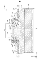
図1は、第1実施形態における半導体装置100の構成を模式的に示す断面図である。図1には、相互に直交するXYZ軸が図示されている。図1のXYZ軸のうち、X軸は、図1の紙面左から紙面右に向かう軸である。+X軸方向は、紙面右に向かう方向であり、−X軸方向は、紙面左に向かう方向である。図1のXYZ軸のうち、Y軸は、図1の紙面手前から紙面奥に向かう軸である。+Y軸方向は、紙面奥に向かう方向であり、−Y軸方向は、紙面手前に向かう方向である。図1のXYZ軸のうち、Z軸は、図1の紙面下から紙面上に向かう軸である。+Z軸方向は、紙面上に向かう方向であり、−Z軸方向は、紙面下に向かう方向である。図1のXYZ軸は、他の図のXYZ軸に対応する。
A. First Embodiment A-1. Configuration of Semiconductor Device FIG. 1 is a cross-sectional view schematically showing a configuration of a
本実施形態では、半導体装置100は、窒化ガリウム(GaN)を用いて形成されたGaN系の半導体装置である。本実施形態では、半導体装置100は、縦型ショットキーバリアダイオードである。本実施形態では、半導体装置100は、電力制御に用いられ、パワーデバイスとも呼ばれる。半導体装置100は、基板110と、半導体層112と、絶縁膜160と、アノード電極170と、カソード電極190とを備える。
In the present embodiment, the
半導体装置100の基板110は、X軸およびY軸に沿って広がる板状を成す半導体である。本実施形態では、基板110は、窒化ガリウム(GaN)から主に成る。本明細書の説明において、「窒化ガリウム(GaN)から主に成る」とは、モル分率において窒化ガリウム(GaN)を90%以上含有することを意味する。本実施形態では、基板110は、ケイ素(Si)をドナー元素として含有するn型半導体である。本実施形態では、基板110に含まれるケイ素(Si)濃度の平均値は、約1×1018cm−3である。
The
半導体装置100の半導体層112は、基板110の+Z軸方向側に位置し、X軸およびY軸に沿って広がるn型半導体層である。本実施形態では、半導体層112は、窒化ガリウム(GaN)から主に成る。本実施形態では、半導体層112は、ケイ素(Si)をドナー元素として含有する。本実施形態では、半導体層112に含まれるケイ素(Si)濃度の平均値は、約1×1016cm−3である。本実施形態では、半導体層112は、有機金属気相成長法(MOCVD:Metal Organic Chemical Vapor Deposition)によって形成された半導体層である。
The
半導体層112は、メサ構造112mと、周囲面112pとを有する。半導体層112のメサ構造112mは、上面112uと側面112sとを有する台地状を成す。本実施形態では、メサ構造112mは、周囲面112pより+Z軸方向に突出した構造である。半導体層112の周囲面112pは、メサ構造112mの周囲に広がる表面である。本実施形態では、メサ構造112mおよび周囲面112pは、ドライエッチングによって形成された構造である。本実施形態では、半導体層112の厚み(Z軸方向の長さ)は、メサ構造112mの部分において約10μm(マイクロメートル)である。
The
半導体装置100において、基点P1は、上面112uにおける絶縁膜160の端部であり、本実施形態では、半導体層112とアノード電極170とのショットキー接合の端部でもある。半導体装置100において、基点P2は、上面112uの端部である。半導体装置100において、基点P3は、メサ構造112mと周囲面112pとの境界である。
In the
基点P1における電界集中を抑制する観点から、メサ構造112mの高さHmは、絶縁膜160の厚みより高いことが好ましい。加工性を確保する観点から、メサ構造112mの高さHmは、5μm以下であることが好ましい。基点P1における電界集中を抑制する観点から、周囲面112pに対する側面112sの角度Amは、10°以上90°以下であることが好ましい。
From the viewpoint of suppressing electric field concentration at the base point P1, the height Hm of the
半導体装置100の絶縁膜160は、電気絶縁性を有する膜である。絶縁膜160は、周囲面112pから側面112sを通じて上面112uの上方にわたって形成されている。本実施形態では、絶縁膜160は、周囲面112pから側面112sを通じて上面112uにわたって形成されている。絶縁膜160は、上面部162と、側面部164と、周囲部166とを有する。
The insulating
絶縁膜160の上面部162は、上面112uの上方に形成された部位である。上面部162は、基点P2より内側に開口部168を画定する。開口部168は、上面112uが露出するまで絶縁膜160の一部を上面112uの上からウェットエッチングによって除去した構造である。開口部168の端部は、基点P1を形成する。
The
上面部162の膜厚は、開口部168に向かうにつれて薄くなる。上面部162は、開口部168を形成するウェットエッチングのエッチャントをマスクとの間に入り込ませることによって薄肉化した構造である。絶縁膜160の基点P4は、上面部162の+Z軸方向側の表面部位のうち膜厚の変化率が変化する部位である。絶縁膜160の基点P5は、絶縁膜160の部位のうち上面112uから+Z軸方向に最も離れた部位である。本実施形態では、上面部162は、基点P1,P2,P4,P5に囲まれた部位である。
The film thickness of the
絶縁膜160の側面部164は、側面112sに形成された部位である。側面部164は、周囲部166の膜厚t6より薄い膜厚t4から上面部162に向かうにつれて更に膜厚が薄くなる部分を有する。側面部164の膜厚t4は、上面部162の膜厚のうち基点P2における膜厚t2より厚い。側面部164は、開口部168を形成するウェットエッチングのエッチャントをマスクとの間に入り込ませることによって薄肉化した構造である。絶縁膜160の基点P6は、絶縁膜160の+Z軸方向側の表面部位のうちメサ構造112mに沿って+Z軸方向に立ち上がる起点である。本実施形態では、側面部164は、基点P2,P3,P5,P6に囲まれた部位である。
The
絶縁膜160の周囲部166は、周囲面112pに形成された部位である。周囲部166の膜厚t6は、上面部162の膜厚のうち基点P2における膜厚t2より厚い。
A
本実施形態では、絶縁膜160は、原子層堆積法(ALD:Atomic Layer Deposition)による厚さ100nmの酸化アルミニウム(Al2O3)から主に成る層に、プラズマ化学気相成長法(プラズマCVD:Plasma Chemical Vapor Deposition)による厚さ500nmの二酸化ケイ素(SiO2)から主に成る層を積層した膜である。
In the present embodiment, the insulating
半導体装置100のアノード電極170は、導電性材料から成り、半導体層112の上面112uにショットキー接合されたショットキー電極である。アノード電極170は、開口部168の内側から、上面部162、側面部164および周囲部166の上にわたって形成されている。これによって、アノード電極170は、半導体層112との間に絶縁膜160を挟むフィールドプレート構造を形成する。本実施形態では、アノード電極170は、上面112uのうち開口部168から露出した部分から、上面部162、側面部164および周囲部166の上にわたって一体的に形成されている。
The
本実施形態では、アノード電極170は、電子ビーム蒸着法によって、半導体層112側から順に、厚さ約100nm(ナノメートル)のニッケル(Ni)から主に成る層と、厚さ約100nmのパラジウム(Pd)から主に成る層と、厚さ約20nmのモリブデン(Mo)から主に成る層とを積層した電極である。アノード電極170におけるニッケル(Ni)は、半導体層112の窒化ガリウム(GaN)とのショットキー接合を形成する。アノード電極170におけるパラジウム(Pd)は、ショットキー障壁高さを向上させる。アノード電極170におけるモリブデン(Mo)は、アノード電極170の上に他の電極(例えば、配線電極)が形成された場合にバリアメタルとして電極層間における電極材料の相互拡散を防止する。
In the present embodiment, the
半導体装置100のカソード電極190は、導電性材料から成り、基板110の−Z軸方向側にオーミック接合されたオーミック電極である。本実施形態では、カソード電極190は、スパッタ法によってチタン(Ti)から主に成る層にアルミニウム−ケイ素合金(AlSi)から成る層を積層した電極である。
The
A−2.半導体装置の製造方法
図2は、第1実施形態における半導体装置100の製造方法を示す工程図である。半導体装置100の製造者は、基板110の上に半導体層112をエピタキシャル成長によって形成する(工程P110)。本実施形態では、製造者は、有機金属気相成長法(MOCVD)を実現するMOCVD装置を用いたエピタキシャル成長によって、半導体層112を形成する。
A-2. Manufacturing Method of Semiconductor Device FIG. 2 is a process diagram showing a manufacturing method of the
半導体層112を形成した後(工程P110)、製造者は、半導体層112にメサ構造112mを形成する(工程P120)。本実施形態では、製造者は、半導体層112の表面のうちメサ構造112mとして残す部分にマスクを形成した後、塩素(Cl)系のドライエッチングによって半導体層112の一部を除去することによって、半導体層112にメサ構造112mおよび周囲面112pを形成する。その後、製造者は、半導体層112に形成したマスクを除去する。マスクは、二酸化ケイ素(SiO2)から主に成るマスクであってもよいし、フォトレジストから成るマスクであってもよい。
After forming the semiconductor layer 112 (process P110), the manufacturer forms the
メサ構造112mを形成した後(工程P120)、製造者は、半導体層112の+Z軸方向側の表面に、絶縁膜160の元となる絶縁膜を形成する(工程P162)。本実施形態では、製造者は、原子層堆積法(ALD)によって酸化アルミニウム(Al2O3)から主に成る層を形成した後、プラズマ化学気相成長法(プラズマCVD)によって二酸化ケイ素(SiO2)から主に成る層を積層することによって、絶縁膜160の元となる絶縁膜を形成する。
After forming the
絶縁膜160の元となる絶縁膜を形成した後(工程P162)、製造者は、絶縁膜160の元となる絶縁膜をウェットエッチングによって加工することによって、絶縁膜160の開口部168を形成する(工程P164,P168)。
After forming the insulating film serving as the base of the insulating film 160 (process P162), the manufacturer forms the
絶縁膜160の開口部168を形成する際、製造者は、絶縁膜160の元となる絶縁膜の上にマスクを形成する(工程P164)。本実施形態では、製造者は、フォトレジストから成るマスクを絶縁膜の上に形成する。
When the
図3は、製造途中にある半導体装置100dを示す説明図である。半導体装置100dは、絶縁膜160の元となる絶縁膜160dの上にマスク910を形成することによって作製される。マスク910は、絶縁膜160dの部位のうち、上面112uに形成された上面部162dと、側面112sに形成された側面部164dと、周囲面112pに形成された周囲部166dとの各部の上に形成される。マスク910は、絶縁膜160の開口部168に対応する部分にマスク開口部918を有する。半導体装置100dにおいて、上面部162dの膜厚t1は、周囲部166dの膜厚t6に等しい。
FIG. 3 is an explanatory view showing the
本実施形態では、製造者は、疎水化表面処理、エッチング処理、並びに、密着性向上剤を塗布する処理を、絶縁膜160dの表面に対して実施せずに、マスク910を絶縁膜160dに形成する。これによって、絶縁膜160dとマスク910との密着力を抑制できる。他の実施形態では、製造者は、絶縁膜160dに対するマスク910の形成に先立って、プラズマ処理を絶縁膜160dの表面に対して実施してもよい。これによっても、絶縁膜160dとマスク910との密着力を抑制できる。
In this embodiment, the manufacturer forms the
図2の説明に戻り、絶縁膜160dの上にマスク910を形成した後(工程P164)、製造者は、絶縁膜160dの上面部162dに開口部168を形成するとともに、絶縁膜160dの上面部162dおよび側面部164dを薄肉化する(工程P168)。これによって、絶縁膜160が形成される。製造者は、絶縁膜160dにおけるマスク開口部918から露出した部分をエッチャントに晒すことによって、絶縁膜160dの上面部162dに開口部168を形成する。その際、製造者は、マスク開口部918側から絶縁膜160dとマスク910との間にエッチャントを入り込ませることによって、上面部162dおよび側面部164dの各膜厚を薄くする。
Returning to the description of FIG. 2, after forming the
図4は、製造途中にある半導体装置100pを示す説明図である。半導体装置100pは、半導体装置100dに対してウェットエッチングを実施することによって作製される。本実施形態では、絶縁膜160における薄肉化される部位は、上面部162および側面部164の全域である。他の実施形態では、絶縁膜160における薄肉化される部位は、上面部162から側面部164の途中までの範囲であってもよいし、上面部162から周囲部166にわたる範囲であってもよい。
FIG. 4 is an explanatory view showing the
本実施形態では、絶縁膜160dを処理するエッチャントは、バッファードフッ酸(BHF)である。絶縁膜160dとマスク910との間へエッチャントを入り込みやすくする観点から、エッチャントに使用するバッファードフッ酸において、フッ化アンモニウムに対するフッ化水素酸の質量比は、0.1以上であることが好ましく、0.5以上であることがさらに好ましく、1以上であることがいっそう好ましい。絶縁膜160dとマスク910との間へと過度にエッチャントが入り込むことを防止する観点から、エッチャントに使用するバッファードフッ酸において、フッ化アンモニウムに対するフッ化水素酸の質量比は、10以下であることが好ましい。
In this embodiment, the etchant for processing the insulating
図2の説明に戻り、絶縁膜160を形成した後(工程P168)、製造者は、マスク910を除去した上で、アノード電極170を形成する(工程P170)。本実施形態では、製造者は、リフトオフ法を用いた電子ビーム蒸着法によってアノード電極170を形成する。アノード電極170を形成する方法は、電子ビーム蒸着法に限らず、抵抗加熱蒸着法であってもよいし、スパッタ法であってもよい。他の実施形態では、製造者は、上面112uおよび絶縁膜160の全面に電極を形成した後、その電極の一部を除去することによって、アノード電極170を形成してもよい。本実施形態では、製造者は、半導体層112側から順に、ニッケル(Ni)から主に成る層と、パラジウム(Pd)から主に成る層と、モリブデン(Mo)から主に成る層とを積層することによって、アノード電極170を形成する。
Returning to the description of FIG. 2, after forming the insulating film 160 (process P168), the manufacturer removes the
アノード電極170を形成した後(工程P170)、製造者は、カソード電極190を形成する(工程P190)。本実施形態では、製造者は、スパッタ法によってチタン(Ti)から主に成る層にアルミニウム−ケイ素合金(AlSi)から主に成る層を積層することによって、カソード電極190を形成する。
After forming the anode electrode 170 (process P170), the manufacturer forms the cathode electrode 190 (process P190). In this embodiment, the manufacturer forms the
これらの工程を経て、半導体装置100が完成する。他の実施形態では、製造者は、半導体層112を形成した後(工程P110)であれば、カソード電極190を形成する工程(工程P190)を、アノード電極170を形成する工程(工程P170)に先立って実施してもよい。
Through these steps, the
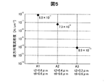
A−3.評価試験
図5は、逆方向電流密度を評価した結果を示すグラフである。試験者は、3つの試料A1,A2,A3について、シミュレーションによって逆方向電流密度を評価した。図5の逆方向電流密度は、各試料に対して500Vを印加した際に測定される逆方向電流密度を示す。
A-3. Evaluation Test FIG. 5 is a graph showing the results of evaluating the reverse current density. The tester evaluated the reverse current density by simulation for three samples A1, A2, and A3. The reverse current density in FIG. 5 indicates the reverse current density measured when 500 V is applied to each sample.
試料A1は、フッ化アンモニウムに対するフッ化水素酸の質量比が0.1未満であるバッファードフッ酸をエッチャントに用いて、絶縁膜160の開口部168を形成することによって、側面部164が薄肉化されていない点を除き、図1の半導体装置100と同様である。試料A1の絶縁膜160において、上面部162の膜厚t2は0.6μmであり、周囲部166の膜厚t6は0.6μmである。
In the sample A1, the
試料A2は、フッ化アンモニウムに対するフッ化水素酸の質量比が試料A3より低いバッファードフッ酸をエッチャントに用いた半導体装置100である。試料A2の絶縁膜160において、上面部162の膜厚t2は0.4μmであり、周囲部166の膜厚t6は0.6μmである。
Sample A2 is a
試料A3は、フッ化アンモニウムに対するフッ化水素酸の質量比が試料A2より高いバッファードフッ酸をエッチャントに用いた半導体装置100である。試料A3の絶縁膜160において、上面部162の膜厚t2は0.2μmであり、周囲部166の膜厚t6は0.6μmである。
Sample A3 is a
図5の評価結果によれば、上面部162および側面部164における膜厚が薄いほど、逆方向電流密度を抑制できることが分かる。言い換えると、上面部162および側面部164における膜厚が薄いほど、逆方向リーク電流を抑制できる。この結果は、上面部162および側面部164の薄肉化によって、ショットキー接合の端部である基点P1に発生する電界集中が緩和されることに起因する。
According to the evaluation result of FIG. 5, it is understood that the reverse current density can be suppressed as the film thicknesses at the
A−4.効果
以上説明した第1実施形態によれば、絶縁膜160の周囲部166の膜厚t6によってアノード電極170の端部の周辺における絶縁破壊を防止できるとともに、絶縁膜160の側面部164における薄肉化によって逆方向リーク電流を抑制できる。また、絶縁膜160に開口部168を形成する工程P168において側面部164を薄肉化する製造方法を適用できる。これらのことから、製造工程の煩雑化を回避しながら、絶縁破壊の防止と逆方向リーク電流の抑制とを両立できる。
A-4. Effect According to the first embodiment described above, the film thickness t6 of the
B.第2実施形態
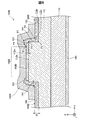
図6は、第2実施形態における半導体装置100Bの構成を模式的に示す断面図である。半導体装置100Bの構成は、絶縁膜160およびアノード電極170に代えて、アノード電極150Bと、絶縁膜160Bと、配線電極180Bとを備える点を除き、第1実施形態の半導体装置100と同様である。
B. Second Embodiment FIG. 6 is a cross-sectional view schematically showing a configuration of a
半導体装置100Bのアノード電極150Bは、導電性材料から成り、半導体層112の上面112uにショットキー接合されたショットキー電極である。アノード電極150Bは、上面112uに形成された第1の電極である。本実施形態では、アノード電極150Bは、電子ビーム蒸着法によって、半導体層112側から順に、厚さ約100nmのニッケル(Ni)から主に成る層と、厚さ約100nmのパラジウム(Pd)から主に成る層と、厚さ約20nmのモリブデン(Mo)から主に成る層とを積層した電極である。
The
半導体装置100Bの絶縁膜160Bは、周囲面112pから側面112sを通じてアノード電極150Bの上にわたって形成され、アノード電極150Bの上に開口部168Bを有する点を除き、第1実施形態の絶縁膜160と同様である。本実施形態では、絶縁膜160の側面部164は、基点P5の周辺に段差を有する。他の実施形態では、側面部164は、基点P5から基点P6にかけてなだらかであってもよい。
The insulating
半導体装置100Bの配線電極180Bは、アノード電極150Bのうち開口部168Bから露出した部分から、上面部162、側面部164および周囲部166の上にわたって一体的に形成された第2の電極である。これによって、配線電極180Bは、半導体層112との間に絶縁膜160Bを挟むフィールドプレート構造を形成する。
The
本実施形態では、配線電極180Bは、スパッタ法によって、アノード電極150Bおよび絶縁膜160Bの側から順に、厚さ約20nmのチタン(Ti)から主に成る層と、厚さ約200nmの窒化チタン(TiN)から主に成る層と、厚さ約20nmのチタン(Ti)から主に成る層と、厚さ約2000nmのアルミニウム−ケイ素合金(AlSi)から主に成る層とを積層した電極である。配線電極180におけるチタン(Ti)は、隣接する電極層および絶縁膜160との密着性を向上させる。配線電極180Bにおける窒化チタン(TiN)は、バリアメタルとして電極層間における電極材料の相互拡散を防止する。配線電極180Bにおけるアルミニウム−ケイ素合金(AlSi)は、配線電極180における電気抵抗を抑制する。
In this embodiment, the
図7は、第2実施形態における半導体装置100Bの製造方法を示す工程図である。半導体装置100Bの製造者は、第1実施形態と同様に半導体層112にメサ構造112mを形成した後(工程P120)、アノード電極150Bを形成する(工程P150)。本実施形態では、製造者は、リフトオフ法を用いた電子ビーム蒸着法によってアノード電極150Bを形成する。アノード電極150Bを形成する方法は、電子ビーム蒸着法に限らず、抵抗加熱蒸着法であってもよいし、スパッタ法であってもよい。他の実施形態では、製造者は、半導体層112の全面に電極を形成した後、その電極の一部を除去することによって、アノード電極150Bを形成してもよい。本実施形態では、製造者は、半導体層112側から順に、ニッケル(Ni)から主に成る層と、パラジウム(Pd)から主に成る層と、モリブデン(Mo)から主に成る層とを積層することによって、アノード電極150Bを形成する。
FIG. 7 is a process diagram illustrating a method for manufacturing the
アノード電極150Bを形成した後(工程P150)、製造者は、半導体層112の+Z軸方向側の表面およびアノード電極150Bの表面に、絶縁膜160Bの元となる絶縁膜を形成する(工程P162B)。本実施形態では、製造者は、原子層堆積法(ALD)によって酸化アルミニウム(Al2O3)から主に成る層を形成した後、プラズマ化学気相成長法(プラズマCVD)によって二酸化ケイ素(SiO2)から主に成る層を積層することによって、絶縁膜160Bの元となる絶縁膜を形成する。
After forming the
絶縁膜160Bの元となる絶縁膜を形成した後(工程P162B)、製造者は、第1実施形態と同様に、絶縁膜160Bの元となる絶縁膜をウェットエッチングによって加工することによって、絶縁膜160Bの開口部168Bを形成する(工程P164B,P168B)。これによって、薄肉化された上面部162および側面部164を有する絶縁膜160Bが形成される。
After forming the insulating film serving as the base of the insulating
絶縁膜160を形成した後(工程P168B)、製造者は、配線電極180Bを形成する(工程P180)。本実施形態では、製造者は、アノード電極150Bおよび絶縁膜160Bの側から順に、厚さ約20nmのチタン(Ti)から主に成る層と、厚さ約200nmの窒化チタン(TiN)から主に成る層と、厚さ約20nmのチタン(Ti)から主に成る層と、厚さ約2000nmのアルミニウム−ケイ素合金(AlSi)から主に成る層とを積層することによって、配線電極180Bを形成する。本実施形態では、製造者は、配線電極180Bの元となる電極をアノード電極150Bおよび絶縁膜160Bの全面にスパッタ法によって形成する。その後、製造者は、配線電極180として残す部分にマスク(フォトレジスト)を形成した後、塩素(Cl)系のドライエッチングによって電極の一部を除去することによって、配線電極180Bを形成する。その後、製造者は、配線電極180Bの上に形成されているマスクを除去する。
After forming the insulating film 160 (process P168B), the manufacturer forms the
配線電極180Bを形成した後(工程P180)、製造者は、第1実施形態と同様にカソード電極190を形成する(工程P190)。これらの工程を経て、半導体装置100が完成する。他の実施形態では、製造者は、半導体層112を形成した後(工程P110)であれば、カソード電極190を形成する工程(工程P190)を、配線電極180Bを形成する工程(工程P180)に先立って実施してもよい。
After forming the
以上説明した第2実施形態によれば、第1実施形態と同様に、製造工程の煩雑化を回避しながら、絶縁破壊の防止と逆方向リーク電流の抑制とを両立できる。 According to the second embodiment described above, it is possible to achieve both prevention of dielectric breakdown and suppression of reverse leakage current while avoiding complication of the manufacturing process, as in the first embodiment.
C.第3実施形態
図8は、第3実施形態における半導体装置100Bの製造方法を示す工程図である。第2実施形態の半導体装置100Bは、その製造方法が異なる点を除き、第2実施形態と同様である。
C. Third Embodiment FIG. 8 is a process diagram showing a method for manufacturing a
第2実施形態と同様に半導体層112を形成した後(工程P110)、製造者は、アノード電極150Bの元となる電極層を半導体層112の全面にわたって形成する(工程P250)。本実施形態では、製造者は、電子ビーム蒸着法によって電極層を形成する。電極層を形成する方法は、電子ビーム蒸着法に限らず、抵抗加熱蒸着法であってもよいし、スパッタ法であってもよい。
After forming the
アノード電極150Bの元となる電極層を形成した後(工程P250)、製造者は、マスクを用いたドライエッチングによって、アノード電極150Bおよびメサ構造112mを形成する(工程P255)。本実施形態では、製造者は、メサ構造112mに対応するマスク(フォトレジスト)を形成した後、塩素(Cl)系のドライエッチングによって半導体層112の一部および電極層の一部を除去することによって、アノード電極150Bおよびメサ構造112mを形成する。アノード電極150Bおよびメサ構造112mを形成した後(工程P255)、製造者は、第2実施形態と同様に、絶縁膜160Bを形成し(工程P162B,P164B,P168B)、それ以降の工程を実施する。
After forming the electrode layer that becomes the base of the
以上説明した第3実施形態によれば、第2実施形態と同様に、製造工程の煩雑化を回避しながら、絶縁破壊の防止と逆方向リーク電流の抑制とを両立できる。また、アノード電極150Bの端部と上面112uの端部との間の距離を抑制できるため、アノード電極150Bの端部における電解集中を効果的に抑制できる。
According to the third embodiment described above, it is possible to achieve both prevention of dielectric breakdown and suppression of reverse leakage current while avoiding complication of the manufacturing process, as in the second embodiment. In addition, since the distance between the end portion of the
D.第4実施形態
図9は、第4実施形態における半導体装置100Bの製造方法を示す工程図である。第4実施形態の半導体装置100Bは、その製造方法が異なる点を除き、第2実施形態と同様である。
D. Fourth Embodiment FIG. 9 is a process diagram illustrating a method for manufacturing a
第2実施形態と同様に半導体層112を形成した後(工程P110)、製造者は、半導体層112の上にアノード電極150Bを形成する(工程P350)。本実施形態では、製造者は、リフトオフ法を用いた電子ビーム蒸着法によってアノード電極150Bを形成する。アノード電極150Bを形成する方法は、電子ビーム蒸着法に限らず、抵抗加熱蒸着法であってもよいし、スパッタ法であってもよい。他の実施形態では、製造者は、半導体層112の全面に電極を形成した後、その電極の一部を除去することによって、アノード電極150Bを形成してもよい。
After forming the
アノード電極150Bを形成した後(工程P350)、製造者は、アノード電極150Bをマスクとして用いたドライエッチングによって、半導体層112にメサ構造112mを形成する(工程P355)。本実施形態では、製造者は、塩素(Cl)系のドライエッチングによって半導体層112の一部を除去することによって、半導体層112にメサ構造112mを形成する。メサ構造112mを形成した後(工程P355)、製造者は、第2実施形態と同様に、絶縁膜160Bを形成し(工程P162B,P164B,P168B)、それ以降の工程を実施する。
After forming the
以上説明した第4実施形態によれば、第2実施形態と同様に、製造工程の煩雑化を回避しながら、絶縁破壊の防止と逆方向リーク電流の抑制とを両立できる。また、アノード電極150Bを利用した自己整合によって、メサ構造112mを形成するマスクを別途作製する必要がないため、製造コストを抑制できる。また、アノード電極150Bの端部と上面112uの端部との間の距離を抑制できるため、アノード電極150Bの端部における電解集中を効果的に抑制できる。
According to the fourth embodiment described above, as in the second embodiment, both prevention of dielectric breakdown and suppression of reverse leakage current can be achieved while avoiding complicated manufacturing processes. Further, since it is not necessary to separately prepare a mask for forming the
E.第5実施形態
図10は、第5実施形態における半導体装置100Eの構成を模式的に示す断面図である。本実施形態では、半導体装置100Eは、縦型pn接合ダイオードである。半導体装置100Eは、半導体層112およびアノード電極170に代えて、半導体層112Eと、半導体層114Eと、アノード電極170Eとを備える点を除き、第1実施形態の半導体装置100と同様である。
E. Fifth Embodiment FIG. 10 is a cross-sectional view schematically showing the configuration of a
半導体装置100Eの半導体層112Eは、基板110の+Z軸方向側に位置し、X軸およびY軸に沿って広がるn型半導体層である。半導体層112Eは、メサ構造112mの+Z軸方向側に半導体層114Eが積層されている点を除き、第1実施形態の半導体層112と同様である。
The
半導体装置100Eの半導体層114Eは、メサ構造112mにおいて半導体層112Eの+Z軸方向側にX軸およびY軸に沿って広がるp型半導体層である。本実施形態では、半導体層114Eは、窒化ガリウム(GaN)から主に成る。本実施形態では、半導体層114Eは、マグネシウム(Mg)をアクセプタとして含有する。半導体装置100Eにおいて、基点P7は、半導体層112Eと半導体層114Eとのpn接合界面の端部であり、側面112sに位置する。
The
半導体装置100Eのアノード電極170Eは、導電性材料から成り、半導体層114Eの上面112uにオーミック接合されたオーミック電極である。アノード電極170Eは、開口部168の内側から、上面部162、側面部164および周囲部166の上にわたって形成されている。これによって、アノード電極170Eは、半導体層112E,114Eとの間に絶縁膜160を挟むフィールドプレート構造を形成する。本実施形態では、アノード電極170Eは、上面112uのうち開口部168から露出した部分から、上面部162、側面部164および周囲部166の上にわたって一体的に形成されている。本実施形態では、アノード電極170Eは、半導体層114E側から順に、ニッケル(Ni)から主に成る層と、金(Au)から主に成る層とを積層した電極である。
The
以上説明した第5実施形態によれば、上面部162および側面部164の薄肉化によって、pn接合界面の端部である基点P7に発生する電界集中を緩和できる。そのため、第1実施形態と同様に、製造工程の煩雑化を回避しながら、絶縁破壊の防止と逆方向リーク電流の抑制とを両立できる。
According to the fifth embodiment described above, the electric field concentration generated at the base point P7 that is the end of the pn junction interface can be alleviated by thinning the
F.他の実施形態
本発明は、上述の実施形態や実施例、変形例に限られるものではなく、その趣旨を逸脱しない範囲において種々の構成で実現することができる。例えば、発明の概要の欄に記載した各形態中の技術的特徴に対応する実施形態、実施例、変形例中の技術的特徴は、上述の課題の一部または全部を解決するために、あるいは、上述の効果の一部または全部を達成するために、適宜、差し替えや、組み合わせを行うことが可能である。また、その技術的特徴が本明細書中に必須なものとして説明されていなければ、適宜、削除することが可能である。
F. Other Embodiments The present invention is not limited to the above-described embodiments, examples, and modifications, and can be realized with various configurations without departing from the spirit thereof. For example, the technical features in the embodiments, examples, and modifications corresponding to the technical features in each embodiment described in the summary section of the invention are to solve some or all of the above-described problems, or In order to achieve part or all of the above-described effects, replacement or combination can be performed as appropriate. Further, if the technical feature is not described as essential in the present specification, it can be deleted as appropriate.
本発明が適用される半導体装置は、上述の実施形態で説明した半導体装置に限らず、メサ構造にフィールドプレート構造を組み合わせた半導体装置であればよい。例えば、ショットキーバリアダイオードである第2実施形態の半導体装置100Bを、第5実施形態と同様に、pn接合ダイオードに適用してもよい。
The semiconductor device to which the present invention is applied is not limited to the semiconductor device described in the above embodiment, and may be any semiconductor device in which a field plate structure is combined with a mesa structure. For example, the
上述の実施形態において、n型半導体層に含まれるドナー元素は、ケイ素(Si)に限らず、ゲルマニウム(Ge)、酸素(O)などであってもよい。上述の実施形態において、p型半導体層に含まれるアクセプタ元素は、マグネシウム(Mg)に限らず、亜鉛(Zn)、炭素(C)などであってもよい。
上述の実施形態において、基板の材質は、窒化ガリウム(GaN)に限らず、ケイ素(Si)、サファイア(Al2O3)および炭化ケイ素(SiC)などのいずれであってもよい。
In the above-described embodiment, the donor element contained in the n-type semiconductor layer is not limited to silicon (Si), but may be germanium (Ge), oxygen (O), or the like. In the above-described embodiment, the acceptor element contained in the p-type semiconductor layer is not limited to magnesium (Mg), but may be zinc (Zn), carbon (C), or the like.
In the above-described embodiment, the material of the substrate is not limited to gallium nitride (GaN), and may be any of silicon (Si), sapphire (Al 2 O 3 ), silicon carbide (SiC), and the like.
上述の実施形態において、半導体層の材質は、窒化ガリウム(GaN)に限らず、ケイ素(Si)、ゲルマニウム(Ge)、III-V族化合物(例えば、窒化アルミニウムガリウム(AlGaN)、窒化インジウムガリウム(InGaN)、ヒ化ガリウム(GaAs)、リン化インジウム(InP)など)、炭化ケイ素(SiC)、酸化ガリウム(Ga2O3)、ワイドバンドギャップ半導体(例えば、ダイヤモンド)などのいずれであってもよい。半導体層は、1つの半導体層であってもよいし、複数の半導体層であってもよい。 In the above-described embodiment, the material of the semiconductor layer is not limited to gallium nitride (GaN), but silicon (Si), germanium (Ge), III-V group compounds (for example, aluminum gallium nitride (AlGaN), indium gallium nitride ( InGaN), gallium arsenide (GaAs), indium phosphide (InP), etc.), silicon carbide (SiC), gallium oxide (Ga 2 O 3 ), wide band gap semiconductor (eg, diamond), etc. Good. The semiconductor layer may be a single semiconductor layer or a plurality of semiconductor layers.
上述の実施形態において、ショットキー電極の材質は、ニッケル(Ni)、パラジウム(Pd)、白金(Pt)、金(Au)、モリブデン(Mo)およびイリジウム(Ir)の少なくとも1つであればよい。ショットキー電極は、1つの電極層であってもよいし、複数の電極層であってもよい。 In the above-described embodiment, the material of the Schottky electrode may be at least one of nickel (Ni), palladium (Pd), platinum (Pt), gold (Au), molybdenum (Mo), and iridium (Ir). . The Schottky electrode may be one electrode layer or a plurality of electrode layers.
上述の実施形態において、配線電極の材質は、アルミニウム(Al)、チタン(Ti)、モリブデン(Mo)、バナジウム(V)、タンタル(Ta)、金(Au)および銅(Cu)の少なくとも1つであればよい。これによって、電気抵抗を抑制しつつ絶縁膜との密着性を十分に確保できる。配線電極は、1つの電極層であってもよいし、複数の電極層であってもよい。例えば、配線電極は、アルミニウム(Al)から主に成る1つの電極層であってもよいし、アルミニウム−ケイ素合金(AlSi)から主に成る1つの電極層であってもよい。配線電極は、ショットキー電極および絶縁膜の側から順に、チタン(Ti)から主に成る層と、窒化チタン(TiN)から主に成る層と、チタン(Ti)から主に成る層と、アルミニウム(Al)から主に成る層とを積層した電極であってもよい。配線電極は、ショットキー電極および絶縁膜の側から順に、タンタル(Ta)から主に成る層と、銅(Cu)から主に成る層とを積層した電極であってもよい。配線電極は、ショットキー電極および絶縁膜の側から順に、窒化タンタル(TaN)から主に成る層と、銅(Cu)から主に成る層とを積層した電極であってもよい。 In the above-described embodiment, the material of the wiring electrode is at least one of aluminum (Al), titanium (Ti), molybdenum (Mo), vanadium (V), tantalum (Ta), gold (Au), and copper (Cu). If it is. Thus, sufficient adhesion with the insulating film can be secured while suppressing electrical resistance. The wiring electrode may be one electrode layer or a plurality of electrode layers. For example, the wiring electrode may be one electrode layer mainly made of aluminum (Al) or one electrode layer mainly made of aluminum-silicon alloy (AlSi). The wiring electrode includes, in order from the Schottky electrode and the insulating film side, a layer mainly made of titanium (Ti), a layer mainly made of titanium nitride (TiN), a layer mainly made of titanium (Ti), and aluminum. It may be an electrode in which a layer mainly composed of (Al) is laminated. The wiring electrode may be an electrode in which a layer mainly made of tantalum (Ta) and a layer mainly made of copper (Cu) are stacked in this order from the Schottky electrode and the insulating film side. The wiring electrode may be an electrode in which a layer mainly made of tantalum nitride (TaN) and a layer mainly made of copper (Cu) are stacked in this order from the Schottky electrode and the insulating film side.
上述の実施形態において、絶縁膜の材質は、二酸化ケイ素(SiO2)、酸化アルミニウム(Al2O3)、窒化ケイ素(SiNx)、酸窒化ケイ素(SiON)、酸窒化ジルコニウム(ZrON)、酸窒化アルミニウム(AlON)、酸化ジルコニウム(ZrO2)および酸化ハフニウム(HfO)の少なくとも1つであればよい。これによって、逆方向リーク電流を十分に抑制できる。絶縁膜は、1つの絶縁層であってもよいし、複数の絶縁層であってもよい。例えば、絶縁膜は、窒化ケイ素(SiNx)から主になる1つの絶縁層であってもよい。絶縁膜の最外層は、窒化ケイ素(SiNx)から主になる層であってもよい。これによって、二酸化ケイ素(SiO2)と比較して、絶縁膜とマスクとの密着力を抑制できるため、絶縁膜とマスクとの間にエッチャントを容易に入り込ませることができる。 In the above-described embodiment, the material of the insulating film is silicon dioxide (SiO 2 ), aluminum oxide (Al 2 O 3 ), silicon nitride (SiNx), silicon oxynitride (SiON), zirconium oxynitride (ZrON), oxynitride It may be at least one of aluminum (AlON), zirconium oxide (ZrO 2 ), and hafnium oxide (HfO). Thereby, the reverse leakage current can be sufficiently suppressed. The insulating film may be one insulating layer or a plurality of insulating layers. For example, the insulating film may be one insulating layer mainly made of silicon nitride (SiNx). The outermost layer of the insulating film may be a layer mainly made of silicon nitride (SiN x ). Accordingly, since the adhesion between the insulating film and the mask can be suppressed as compared with silicon dioxide (SiO 2 ), the etchant can easily enter between the insulating film and the mask.
100,100B,100E,100d,100p…半導体装置
110…基板
112…半導体層
112E…半導体層
112m…メサ構造
112p…周囲面
112s…側面
112u…上面
114E…半導体層
150B…アノード電極
160,160B,160d…絶縁膜
162,162d…上面部
164,164d…側面部
166,166d…周囲部
168,168B…開口部
170,170E…アノード電極
180,180B…配線電極
190…カソード電極
910…マスク
918…マスク開口部
100, 100B, 100E, 100d, 100p ...
Claims (17)
上面と側面とを有する台地状を成すメサ構造と、前記メサ構造の周囲に広がる周囲面と、を有する半導体層と、
前記周囲面から前記側面を通じて前記上面の上方にわたって形成された絶縁膜であって、前記上面の上方に形成され前記上面の端部より内側に開口部を画定する上面部と、前記側面に形成された側面部と、前記周囲面に形成された周囲部と、を有する絶縁膜と、
前記開口部の内側から、前記上面部、前記側面部および前記周囲部の上にわたって形成された電極と
を備え、
前記側面部は、前記周囲部より薄い膜厚から前記上面部に向かうにつれて更に膜厚が薄くなる部分を、有し、
前記上面部の膜厚は、前記開口部に向かうにつれて薄くなり、
前記電極は、前記上面にショットキー接合されたショットキー電極を含み、
前記絶縁膜の膜厚は、前記周囲部と前記側面部と前記上面部とのうち、前記周囲部が最も大きく、前記側面部が第2番目に大きく、前記上面部が最も小さい、半導体装置。 A semiconductor device,
A semiconductor layer having a plateau-like mesa structure having an upper surface and side surfaces, and a peripheral surface extending around the mesa structure;
An insulating film formed from the peripheral surface to the upper surface through the side surface, the upper surface portion being formed above the upper surface and defining an opening inside the end portion of the upper surface; and formed on the side surface. An insulating film having a side surface portion and a peripheral portion formed on the peripheral surface;
An electrode formed from the inside of the opening to the top surface, the side surface, and the peripheral portion;
The side surface portion has a portion where the film thickness becomes thinner as it goes from the film thickness thinner than the peripheral part to the upper surface part,
The film thickness of the upper surface portion becomes thinner toward the opening,
The electrode includes a Schottky electrode that is Schottky bonded to the upper surface,
The thickness of the insulating film is a semiconductor device in which the peripheral part is the largest, the side part is the second largest, and the top part is the smallest among the peripheral part, the side part, and the top part.
前記絶縁膜は、前記周囲面から前記側面を通じて前記上面にわたって形成され、
前記電極は、前記上面のうち前記開口部から露出した部分から、前記上面部、前記側面部および前記周囲部の上にわたって一体的に形成された、半導体装置。 The semiconductor device according to claim 1,
The insulating film is formed from the peripheral surface to the upper surface through the side surface,
The electrode is a semiconductor device formed integrally from a portion of the upper surface exposed from the opening to the upper surface portion, the side surface portion, and the peripheral portion.
前記電極は、第1の電極と、第2の電極とを含み、
前記第1の電極は、前記上面に形成され、
前記絶縁膜は、前記周囲面から前記側面を通じて前記第1の電極の上にわたって形成され、
前記第2の電極は、前記第1の電極のうち前記開口部から露出した部分から、前記上面部、前記側面部および前記周囲部の上にわたって一体的に形成された、半導体装置。 The semiconductor device according to claim 1 or 2, wherein
The electrode includes a first electrode and a second electrode,
The first electrode is formed on the upper surface,
The insulating film is formed on the first electrode from the peripheral surface through the side surface,
The second electrode is a semiconductor device formed integrally from a portion of the first electrode exposed from the opening to the upper surface, the side surface, and the peripheral portion.
上面と側面とを有する台地状を成すメサ構造と、前記メサ構造の周囲に広がる周囲面とを、半導体層に形成する工程と、
前記周囲面から前記側面を通じて前記上面の上方にわたって絶縁膜を形成する工程であって、前記上面の上方に形成され前記上面の端部より内側に開口部を画定する上面部と、前記側面に形成された側面部と、前記周囲面に形成された周囲部と、を有する絶縁膜を形成する工程と、
ウェットエッチングによって前記絶縁膜における前記開口部を形成する工程と、
前記開口部の内側から、前記上面部、前記側面部および前記周囲部の上にわたって電極を形成する工程と
を備え、
前記開口部を形成する工程は、
前記開口部に対応する部分にマスク開口部を有するマスクを、前記絶縁膜の部位のうち、前記上面部と、前記側面部と、前記周囲部との各部の上に形成する工程と、
前記マスクを形成した後、前記絶縁膜における前記マスク開口部から露出した部分をエッチャントに晒すことによって前記開口部を形成する際、前記絶縁膜と前記マスクとの間に前記エッチャントを入り込ませることによって、前記周囲部より薄い膜厚から前記上面部に向かうにつれて更に膜厚が薄くなる部分を、前記側面部に形成する工程と
を含み、
前記上面部の膜厚は、前記開口部に向かうにつれて薄くなり、
前記電極は、前記上面にショットキー接合されたショットキー電極を含む、半導体装置の製造方法。 A method for manufacturing a semiconductor device, comprising:
Forming a plateau-shaped mesa structure having an upper surface and a side surface and a peripheral surface extending around the mesa structure in a semiconductor layer;
Forming an insulating film over the upper surface from the peripheral surface through the side surface, the upper surface portion being formed above the upper surface and defining an opening inside the end portion of the upper surface; and formed on the side surface Forming an insulating film having a side surface portion formed on the peripheral surface and a peripheral portion formed on the peripheral surface;
Forming the opening in the insulating film by wet etching;
Forming an electrode over the upper surface portion, the side surface portion, and the peripheral portion from the inside of the opening, and
The step of forming the opening includes
Forming a mask having a mask opening in a portion corresponding to the opening on each of the upper surface portion, the side surface portion, and the peripheral portion of the portion of the insulating film;
After forming the mask, when the opening is formed by exposing a portion of the insulating film exposed from the mask opening to an etchant, the etchant is inserted between the insulating film and the mask. A step of forming on the side surface a portion whose film thickness becomes thinner as it goes from the film thickness thinner than the peripheral part to the upper surface part,
The film thickness of the upper surface portion becomes thinner toward the opening,
The method of manufacturing a semiconductor device, wherein the electrode includes a Schottky electrode bonded to the upper surface.
前記絶縁膜を形成する工程は、前記周囲面から前記側面を通じて前記上面にわたって前記絶縁膜を形成する工程であり、
前記電極を形成する工程は、前記上面のうち前記開口部から露出した部分から、前記上面部、前記側面部および前記周囲部の上にわたって一体的に前記電極を形成する工程である、半導体装置の製造方法。 A method of manufacturing a semiconductor device according to claim 7 or 8 ,
The step of forming the insulating film is a step of forming the insulating film from the peripheral surface to the upper surface through the side surface,
The step of forming the electrode is a step of integrally forming the electrode from a portion of the upper surface exposed from the opening to the upper surface portion, the side surface portion, and the peripheral portion. Production method.
更に、前記絶縁膜を形成する工程に先立って、前記電極とは異なる他の電極を前記上面に形成する工程を備え、
前記絶縁膜を形成する工程は、前記他の電極を形成した後、前記周囲面から前記側面を通じて前記他の電極の上にわたって前記絶縁膜を形成する工程であり、
前記電極を形成する工程は、前記他の電極のうち前記開口部から露出した部分から、前記上面部、前記側面部および前記周囲部の上にわたって一体的に前記電極を形成する工程である、半導体装置の製造方法。 A method of manufacturing a semiconductor device according to claim 7 or 8 ,
Furthermore, prior to the step of forming the insulating film, the method includes the step of forming another electrode different from the electrode on the upper surface,
The step of forming the insulating film is a step of forming the insulating film over the other electrode from the peripheral surface through the side surface after forming the other electrode,
The step of forming the electrode is a step of forming the electrode integrally from the portion of the other electrode exposed from the opening to the upper surface, the side surface, and the peripheral portion. Device manufacturing method.
Priority Applications (1)
| Application Number | Priority Date | Filing Date | Title |
|---|---|---|---|
| JP2015037512A JP6344264B2 (en) | 2015-02-27 | 2015-02-27 | Semiconductor device and manufacturing method thereof |
Applications Claiming Priority (1)
| Application Number | Priority Date | Filing Date | Title |
|---|---|---|---|
| JP2015037512A JP6344264B2 (en) | 2015-02-27 | 2015-02-27 | Semiconductor device and manufacturing method thereof |
Publications (3)
| Publication Number | Publication Date |
|---|---|
| JP2016162786A JP2016162786A (en) | 2016-09-05 |
| JP2016162786A5 JP2016162786A5 (en) | 2017-06-22 |
| JP6344264B2 true JP6344264B2 (en) | 2018-06-20 |
Family
ID=56847513
Family Applications (1)
| Application Number | Title | Priority Date | Filing Date |
|---|---|---|---|
| JP2015037512A Active JP6344264B2 (en) | 2015-02-27 | 2015-02-27 | Semiconductor device and manufacturing method thereof |
Country Status (1)
| Country | Link |
|---|---|
| JP (1) | JP6344264B2 (en) |
Cited By (1)
| Publication number | Priority date | Publication date | Assignee | Title |
|---|---|---|---|---|
| JP7455535B2 (en) | 2019-09-11 | 2024-03-26 | 旭ダイヤモンド工業株式会社 | Super abrasive tool and method for manufacturing super abrasive tool |
Family Cites Families (4)
| Publication number | Priority date | Publication date | Assignee | Title |
|---|---|---|---|---|
| JPH08139341A (en) * | 1994-11-11 | 1996-05-31 | Murata Mfg Co Ltd | Schottky barrier diode |
| US8502337B2 (en) * | 2008-08-05 | 2013-08-06 | Sumitomo Electric Industries, Ltd. | Schottky barrier diode and method for manufacturing Schottky barrier diode |
| JP6107430B2 (en) * | 2012-06-08 | 2017-04-05 | 豊田合成株式会社 | Semiconductor device |
| JP6241099B2 (en) * | 2013-07-17 | 2017-12-06 | 豊田合成株式会社 | Semiconductor device |
-
2015
- 2015-02-27 JP JP2015037512A patent/JP6344264B2/en active Active
Cited By (1)
| Publication number | Priority date | Publication date | Assignee | Title |
|---|---|---|---|---|
| JP7455535B2 (en) | 2019-09-11 | 2024-03-26 | 旭ダイヤモンド工業株式会社 | Super abrasive tool and method for manufacturing super abrasive tool |
Also Published As
| Publication number | Publication date |
|---|---|
| JP2016162786A (en) | 2016-09-05 |
Similar Documents
| Publication | Publication Date | Title |
|---|---|---|
| JP6260553B2 (en) | Semiconductor device and manufacturing method thereof | |
| JP6241099B2 (en) | Semiconductor device | |
| US9349668B2 (en) | Semiconductor device | |
| US9711661B2 (en) | Semiconductor device and manufacturing method thereof | |
| JP6149786B2 (en) | Semiconductor device and manufacturing method of semiconductor device | |
| JP6179445B2 (en) | Vertical Schottky Barrier Diode, Manufacturing Method for Vertical Schottky Barrier Diode | |
| JP6319151B2 (en) | Semiconductor device and manufacturing method of semiconductor device | |
| JP6344264B2 (en) | Semiconductor device and manufacturing method thereof | |
| US9685348B2 (en) | Semiconductor device, method of manufacturing the same and power converter | |
| US9391150B2 (en) | Semiconductor Device | |
| US9972725B2 (en) | Semiconductor device and manufacturing method of the same | |
| JP6485303B2 (en) | Semiconductor device, method for manufacturing the same, and power conversion device | |
| JP2015204333A (en) | Semiconductor device and method for manufacturing semiconductor device | |
| JP6540547B2 (en) | MPS diode | |
| JP6327139B2 (en) | Semiconductor device and manufacturing method thereof | |
| JP6733588B2 (en) | Method of manufacturing semiconductor device | |
| JP6237553B2 (en) | Semiconductor device and manufacturing method thereof | |
| JP6176131B2 (en) | Manufacturing method of semiconductor device | |
| JP2015204335A (en) | Semiconductor device and method for manufacturing semiconductor device | |
| JP6319141B2 (en) | Semiconductor device | |
| JP6398909B2 (en) | Schottky barrier diode and manufacturing method thereof |
Legal Events
| Date | Code | Title | Description |
|---|---|---|---|
| A621 | Written request for application examination |
Free format text: JAPANESE INTERMEDIATE CODE: A621 Effective date: 20170323 |
|
| A521 | Written amendment |
Free format text: JAPANESE INTERMEDIATE CODE: A523 Effective date: 20170510 |
|
| A131 | Notification of reasons for refusal |
Free format text: JAPANESE INTERMEDIATE CODE: A131 Effective date: 20170829 |
|
| A521 | Written amendment |
Free format text: JAPANESE INTERMEDIATE CODE: A523 Effective date: 20171024 |
|
| A131 | Notification of reasons for refusal |
Free format text: JAPANESE INTERMEDIATE CODE: A131 Effective date: 20180213 |
|
| A521 | Written amendment |
Free format text: JAPANESE INTERMEDIATE CODE: A523 Effective date: 20180411 |
|
| TRDD | Decision of grant or rejection written | ||
| A01 | Written decision to grant a patent or to grant a registration (utility model) |
Free format text: JAPANESE INTERMEDIATE CODE: A01 Effective date: 20180424 |
|
| A61 | First payment of annual fees (during grant procedure) |
Free format text: JAPANESE INTERMEDIATE CODE: A61 Effective date: 20180507 |
|
| R150 | Certificate of patent or registration of utility model |
Ref document number: 6344264 Country of ref document: JP Free format text: JAPANESE INTERMEDIATE CODE: R150 |