JP6328055B2 - EBCCD, method for operating EBCCD, dark field inspection system, inspection method and inspection system - Google Patents
EBCCD, method for operating EBCCD, dark field inspection system, inspection method and inspection system Download PDFInfo
- Publication number
- JP6328055B2 JP6328055B2 JP2014547347A JP2014547347A JP6328055B2 JP 6328055 B2 JP6328055 B2 JP 6328055B2 JP 2014547347 A JP2014547347 A JP 2014547347A JP 2014547347 A JP2014547347 A JP 2014547347A JP 6328055 B2 JP6328055 B2 JP 6328055B2
- Authority
- JP
- Japan
- Prior art keywords
- ccd
- photocathode
- ebccd
- control device
- holes
- Prior art date
- Legal status (The legal status is an assumption and is not a legal conclusion. Google has not performed a legal analysis and makes no representation as to the accuracy of the status listed.)
- Active
Links
- 238000007689 inspection Methods 0.000 title claims description 44
- 238000000034 method Methods 0.000 title claims description 26
- 238000005286 illumination Methods 0.000 claims description 48
- 230000003287 optical effect Effects 0.000 claims description 27
- XUIMIQQOPSSXEZ-UHFFFAOYSA-N Silicon Chemical group [Si] XUIMIQQOPSSXEZ-UHFFFAOYSA-N 0.000 claims description 18
- 239000004065 semiconductor Substances 0.000 claims description 13
- 239000011248 coating agent Substances 0.000 claims description 9
- 238000000576 coating method Methods 0.000 claims description 9
- 230000010354 integration Effects 0.000 claims description 8
- 229910052751 metal Inorganic materials 0.000 claims description 6
- 239000002184 metal Substances 0.000 claims description 6
- 230000000694 effects Effects 0.000 claims description 3
- 230000008569 process Effects 0.000 claims description 3
- ZOXJGFHDIHLPTG-UHFFFAOYSA-N Boron Chemical compound [B] ZOXJGFHDIHLPTG-UHFFFAOYSA-N 0.000 claims description 2
- 239000006117 anti-reflective coating Substances 0.000 claims description 2
- 229910052796 boron Inorganic materials 0.000 claims description 2
- 230000001902 propagating effect Effects 0.000 claims 2
- 238000010586 diagram Methods 0.000 description 20
- 229910052710 silicon Inorganic materials 0.000 description 16
- 239000010703 silicon Substances 0.000 description 16
- 239000000463 material Substances 0.000 description 15
- 230000005684 electric field Effects 0.000 description 10
- 150000002500 ions Chemical class 0.000 description 8
- 101710121996 Hexon protein p72 Proteins 0.000 description 7
- 101710125418 Major capsid protein Proteins 0.000 description 7
- 238000001514 detection method Methods 0.000 description 6
- 230000010287 polarization Effects 0.000 description 6
- 230000008859 change Effects 0.000 description 5
- 238000009826 distribution Methods 0.000 description 5
- 239000002245 particle Substances 0.000 description 5
- 230000005855 radiation Effects 0.000 description 5
- OAICVXFJPJFONN-UHFFFAOYSA-N Phosphorus Chemical compound [P] OAICVXFJPJFONN-UHFFFAOYSA-N 0.000 description 4
- 238000000149 argon plasma sintering Methods 0.000 description 4
- 239000004020 conductor Substances 0.000 description 4
- 238000003384 imaging method Methods 0.000 description 4
- 238000004519 manufacturing process Methods 0.000 description 4
- 230000008901 benefit Effects 0.000 description 3
- 230000007547 defect Effects 0.000 description 3
- 230000001133 acceleration Effects 0.000 description 2
- 238000003491 array Methods 0.000 description 2
- 238000005452 bending Methods 0.000 description 2
- 230000000903 blocking effect Effects 0.000 description 2
- 238000005516 engineering process Methods 0.000 description 2
- 239000012535 impurity Substances 0.000 description 2
- 239000012212 insulator Substances 0.000 description 2
- 238000005259 measurement Methods 0.000 description 2
- VYPSYNLAJGMNEJ-UHFFFAOYSA-N silicon dioxide Inorganic materials O=[Si]=O VYPSYNLAJGMNEJ-UHFFFAOYSA-N 0.000 description 2
- JBRZTFJDHDCESZ-UHFFFAOYSA-N AsGa Chemical compound [As]#[Ga] JBRZTFJDHDCESZ-UHFFFAOYSA-N 0.000 description 1
- JMASRVWKEDWRBT-UHFFFAOYSA-N Gallium nitride Chemical compound [Ga]#N JMASRVWKEDWRBT-UHFFFAOYSA-N 0.000 description 1
- 230000003044 adaptive effect Effects 0.000 description 1
- 229910052783 alkali metal Inorganic materials 0.000 description 1
- 150000001340 alkali metals Chemical class 0.000 description 1
- PNEYBMLMFCGWSK-UHFFFAOYSA-N aluminium oxide Inorganic materials [O-2].[O-2].[O-2].[Al+3].[Al+3] PNEYBMLMFCGWSK-UHFFFAOYSA-N 0.000 description 1
- 230000009286 beneficial effect Effects 0.000 description 1
- 230000005540 biological transmission Effects 0.000 description 1
- 229910052792 caesium Inorganic materials 0.000 description 1
- TVFDJXOCXUVLDH-UHFFFAOYSA-N caesium atom Chemical compound [Cs] TVFDJXOCXUVLDH-UHFFFAOYSA-N 0.000 description 1
- 230000015556 catabolic process Effects 0.000 description 1
- 239000013078 crystal Substances 0.000 description 1
- 230000001419 dependent effect Effects 0.000 description 1
- 239000002019 doping agent Substances 0.000 description 1
- 238000005553 drilling Methods 0.000 description 1
- 238000010891 electric arc Methods 0.000 description 1
- 238000005530 etching Methods 0.000 description 1
- 239000011888 foil Substances 0.000 description 1
- 239000005350 fused silica glass Substances 0.000 description 1
- ORUIBWPALBXDOA-UHFFFAOYSA-L magnesium fluoride Chemical compound [F-].[F-].[Mg+2] ORUIBWPALBXDOA-UHFFFAOYSA-L 0.000 description 1
- 230000007246 mechanism Effects 0.000 description 1
- 239000007769 metal material Substances 0.000 description 1
- 229910052752 metalloid Inorganic materials 0.000 description 1
- 150000002738 metalloids Chemical class 0.000 description 1
- 238000012986 modification Methods 0.000 description 1
- 230000004048 modification Effects 0.000 description 1
- 238000000206 photolithography Methods 0.000 description 1
- 230000001737 promoting effect Effects 0.000 description 1
- 239000011253 protective coating Substances 0.000 description 1
- 239000010453 quartz Substances 0.000 description 1
- 230000009467 reduction Effects 0.000 description 1
- 230000027756 respiratory electron transport chain Effects 0.000 description 1
- 230000004044 response Effects 0.000 description 1
- 229910052594 sapphire Inorganic materials 0.000 description 1
- 239000010980 sapphire Substances 0.000 description 1
- 238000007493 shaping process Methods 0.000 description 1
- 239000002356 single layer Substances 0.000 description 1
- 238000004544 sputter deposition Methods 0.000 description 1
- 239000000758 substrate Substances 0.000 description 1
- 230000003746 surface roughness Effects 0.000 description 1
Images


Classifications
-
- G—PHYSICS
- G01—MEASURING; TESTING
- G01N—INVESTIGATING OR ANALYSING MATERIALS BY DETERMINING THEIR CHEMICAL OR PHYSICAL PROPERTIES
- G01N21/00—Investigating or analysing materials by the use of optical means, i.e. using sub-millimetre waves, infrared, visible or ultraviolet light
- G01N21/84—Systems specially adapted for particular applications
- G01N21/88—Investigating the presence of flaws or contamination
- G01N21/95—Investigating the presence of flaws or contamination characterised by the material or shape of the object to be examined
- G01N21/9501—Semiconductor wafers
-
- H—ELECTRICITY
- H01—ELECTRIC ELEMENTS
- H01J—ELECTRIC DISCHARGE TUBES OR DISCHARGE LAMPS
- H01J31/00—Cathode ray tubes; Electron beam tubes
- H01J31/08—Cathode ray tubes; Electron beam tubes having a screen on or from which an image or pattern is formed, picked up, converted, or stored
- H01J31/26—Image pick-up tubes having an input of visible light and electric output
-
- H—ELECTRICITY
- H01—ELECTRIC ELEMENTS
- H01L—SEMICONDUCTOR DEVICES NOT COVERED BY CLASS H10
- H01L27/00—Devices consisting of a plurality of semiconductor or other solid-state components formed in or on a common substrate
- H01L27/14—Devices consisting of a plurality of semiconductor or other solid-state components formed in or on a common substrate including semiconductor components sensitive to infrared radiation, light, electromagnetic radiation of shorter wavelength or corpuscular radiation and specially adapted either for the conversion of the energy of such radiation into electrical energy or for the control of electrical energy by such radiation
- H01L27/144—Devices controlled by radiation
- H01L27/146—Imager structures
- H01L27/148—Charge coupled imagers
- H01L27/14806—Structural or functional details thereof
- H01L27/14812—Special geometry or disposition of pixel-elements, address lines or gate-electrodes
- H01L27/14818—Optical shielding
-
- G—PHYSICS
- G01—MEASURING; TESTING
- G01N—INVESTIGATING OR ANALYSING MATERIALS BY DETERMINING THEIR CHEMICAL OR PHYSICAL PROPERTIES
- G01N21/00—Investigating or analysing materials by the use of optical means, i.e. using sub-millimetre waves, infrared, visible or ultraviolet light
- G01N21/84—Systems specially adapted for particular applications
- G01N21/88—Investigating the presence of flaws or contamination
- G01N21/8806—Specially adapted optical and illumination features
- G01N2021/8822—Dark field detection
-
- G—PHYSICS
- G01—MEASURING; TESTING
- G01N—INVESTIGATING OR ANALYSING MATERIALS BY DETERMINING THEIR CHEMICAL OR PHYSICAL PROPERTIES
- G01N21/00—Investigating or analysing materials by the use of optical means, i.e. using sub-millimetre waves, infrared, visible or ultraviolet light
- G01N21/84—Systems specially adapted for particular applications
- G01N21/88—Investigating the presence of flaws or contamination
- G01N21/95—Investigating the presence of flaws or contamination characterised by the material or shape of the object to be examined
- G01N21/956—Inspecting patterns on the surface of objects
- G01N2021/95676—Masks, reticles, shadow masks
-
- H—ELECTRICITY
- H01—ELECTRIC ELEMENTS
- H01L—SEMICONDUCTOR DEVICES NOT COVERED BY CLASS H10
- H01L27/00—Devices consisting of a plurality of semiconductor or other solid-state components formed in or on a common substrate
- H01L27/14—Devices consisting of a plurality of semiconductor or other solid-state components formed in or on a common substrate including semiconductor components sensitive to infrared radiation, light, electromagnetic radiation of shorter wavelength or corpuscular radiation and specially adapted either for the conversion of the energy of such radiation into electrical energy or for the control of electrical energy by such radiation
- H01L27/144—Devices controlled by radiation
- H01L27/146—Imager structures
- H01L27/148—Charge coupled imagers
- H01L27/14831—Area CCD imagers
- H01L27/14856—Time-delay and integration
Landscapes
- Physics & Mathematics (AREA)
- General Physics & Mathematics (AREA)
- Power Engineering (AREA)
- Engineering & Computer Science (AREA)
- Health & Medical Sciences (AREA)
- Life Sciences & Earth Sciences (AREA)
- Chemical & Material Sciences (AREA)
- Analytical Chemistry (AREA)
- Biochemistry (AREA)
- General Health & Medical Sciences (AREA)
- Immunology (AREA)
- Pathology (AREA)
- Electromagnetism (AREA)
- Condensed Matter Physics & Semiconductors (AREA)
- Computer Hardware Design (AREA)
- Microelectronics & Electronic Packaging (AREA)
- Solid State Image Pick-Up Elements (AREA)
- Image-Pickup Tubes, Image-Amplification Tubes, And Storage Tubes (AREA)
- Transforming Light Signals Into Electric Signals (AREA)
- Investigating Materials By The Use Of Optical Means Adapted For Particular Applications (AREA)
Description
関連出願
本願は、2011年12月12日に出願された米国特許仮出願第61/569,611号(名称「Electron−Bombarded CCD And Inspection Systems Using Electron−Bombarded CCD Detectors」)に対する優先権を主張するものであり、この米国特許仮出願は、参照により本明細書に組み込まれる。
RELATED APPLICATION This application claims priority to US Provisional Application No. 61 / 569,611, filed December 12, 2011 (named “Electron-Bombarded CCD And Inspection Systems Using Electron-Bombarded CCD Detectors”). And this provisional US patent application is incorporated herein by reference.
開示の背景
本開示は、きわめて低レベルの光を、高い空間分解能、高い量子効率、非常に良好な信号対雑音比、および高いダイナミックレンジで検出することのできる感光性アレイ検出器に関する。
BACKGROUND OF THE DISCLOSURE The present disclosure relates to a photosensitive array detector that can detect very low levels of light with high spatial resolution, high quantum efficiency, very good signal-to-noise ratio, and high dynamic range.
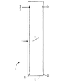
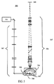
電子衝撃電荷結合素子(EBCCD)検出器は、当技術分野において公知である。図1Aは、従来型EBCCD101の図である。EBCCD101は密封管105を含み、この密封管は、真空環境において感光性光電陰極104とCCD102を格納する。一般に、光電陰極104とCCD102の間のギャップは約1mmか2mmである。密封管105は、光電陰極104に隣接して位置するウィンドウを有するので、入射光110の存在下では、光電陰極104が入射光110からの光子を吸収でき、次いで1つまたは数個の電子112を放出することができる。
Electron impact charge coupled device (EBCCD) detectors are known in the art. FIG. 1A is a diagram of a
典型的な構成では、光電陰極104は、CCD102に対して約−2000V〜−10,000Vの負の電位に保たれる。このような電位差があるため、電子112はCCD102に向かって加速する。電子がCCD102に衝突すると、この電子は通常、CCD102の半導体材料内に複数の電子正孔対を生成する。電子はCCD102に捕捉され、その後、CCD102が検出器から読み出されるときに電流または電圧に変換される。
In a typical configuration, the
イメージ増強検出器も、当技術分野において公知である。イメージ増強管はEBCCDと同様であるが、CCDの代わりに蛍光スクリーンと出力ウィンドウが存在する点が異なる。蛍光スクリーンからの光の捕捉は、CCDやCMOSイメージングデバイス等の外部のイメージ検出器で行うことができる。 Image enhancement detectors are also known in the art. The image intensifier is similar to EBCCD except that a fluorescent screen and an output window are present instead of CCD. Capture of light from the phosphor screen can be performed with an external image detector such as a CCD or CMOS imaging device.
光電子倍増管も、当技術分野において公知である。光電子倍増管は、非常に高い利得を有することができ、場合によっては、単一の捕捉光子を検出することもできる。しかし、個々の光電子倍増管は空間分解能を持たない。光電子倍増管アレイを製作することは可能であるが、大型で高価となり、空間分解能はミクロン単位でなくミリメートル単位の程度である。 Photomultiplier tubes are also known in the art. Photomultiplier tubes can have very high gains and in some cases can detect a single captured photon. However, individual photomultiplier tubes do not have spatial resolution. Although it is possible to produce a photomultiplier tube array, it is large and expensive, and the spatial resolution is in the order of millimeters instead of microns.
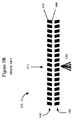
マイクロチャンネルプレート(MCP)検出器も、当技術分野において公知である。MCPは、単独でも使用できるが、カスケード状に配置して利得を増加させることもできる。図1Bは、カスケード状に配置された2つのMCP140、142を含む従来型MCPアセンブリ121の断面図である。典型的なMCPは高抵抗性材料で作られ、厚さは1〜2mmであり得る。MCPは、約6〜20μmの間隔を空けて並んだ直径約4〜10μmの小さな穴の配列を格納する。通常、二次電子の放出(以下に詳述)を確実に最大化する目的で、MCP表面に対する垂線に対して、これらの穴を意図的に数度傾斜させる。図1Bが示す通り、MCP140、142のそれぞれの穴が反対方向に傾斜して、カスケード状のMCPの積み重ねを通過するイオンの直線経路を遮断するか、少なくとも最小化している。MCP140の底面146は、その上面145に対して正の電位(例えば数百ボルト〜1または2kV)に保つことができる。MCP142の電位は、MCP140より正の電位に維持することができる。一般に、カスケード状に配置された複数のMCPを使用する場合、入力から出力に進むにつれて、連続したMCPの各々は、直前の電位よりも正の電位に維持される。
Microchannel plate (MCP) detectors are also known in the art. MCPs can be used alone, but can also be arranged in cascade to increase gain. FIG. 1B is a cross-sectional view of a
作動時は、電子131がいずれかの穴の壁部に衝突すると、二次電子が様々な方向に放出される。MCPの上面と底面の間に電位差があるので、これらの二次電子は下面に向かって加速する。二次電子の一部は、穴の壁部に衝突して、さらに二次電子を生成する。単一のMCP内で、このプロセスが複数回発生し得る。実際、単一の入射電子または入射光子から、様々な方向に移動する数百個、あるいは数千個もの二次電子が生成され得る。カスケード状に配置されたMCP140、142の場合、単一の入射電子または入射光子から、100,000個〜1,000,000個の二次電子132が生成され得る。MCPは、イメージ増強管または光電陰極付きEBCCD(入射光子エネルギーが十分であれば光電陰極無し)の中で使用できる。
In operation, secondary electrons are emitted in various directions when the
不都合なことに、上記の検出器は空間分解能が低いため、半導体検査応用における用途が著しく限定されている。例えば、従来型EBCCD検出器では、電子は、CCDに向かって加速しながら水平方向に広がる。半導体検査で使われるUV光反応性の応用では、入射光子は約3.5eV以上のエネルギーを有する。光電陰極の仕事関数はわずか1eVか2eVであり得るため、1eVまたは数eVのエネルギーで電子が発生する。特に注目すべきことは、1eVもの低エネルギーが約6×10⁵ms−1の電子速度に対応することである。 Unfortunately, due to the low spatial resolution of the above detectors, their use in semiconductor inspection applications is significantly limited. For example, in a conventional EBCCD detector, electrons spread horizontally while accelerating towards the CCD. In UV photoresponsive applications used in semiconductor inspection, incident photons have an energy of about 3.5 eV or more. Since the work function of the photocathode can be only 1 eV or 2 eV, electrons are generated with an energy of 1 eV or several eV. Of particular note is that energy as low as 1 eV corresponds to an electron velocity of about 6 × 10 5 ms −1 .
電子は本質的にランダムな方向に放出されるので、大部分の電子は、相当な水平方向速度成分をもって放出される。106Vm−1の加速場勾配(1mmのギャップの横断に1kV)下では、電子が光電陰極からCCDまでの上記1mmのギャップを渡るのに約100psを要する。この100psの間、典型的な電子1個は、その水平方向速度成分のため約50μm横方向に動く。初期電子エネルギーに応じて水平速度がゼロ〜最大値に分布するので、約50μm〜100μmの長さ尺度の画像ぶれが発生し得る。入射光の波長が短いほど初期光子エネルギーが大きくなり、この画像ぶれが増加する。 Since electrons are emitted in an essentially random direction, most electrons are emitted with a significant horizontal velocity component. Under an acceleration field gradient of 10 6 Vm −1 (1 kV across a 1 mm gap), it takes about 100 ps for electrons to cross the 1 mm gap from the photocathode to the CCD. During this 100 ps, one typical electron moves about 50 μm laterally due to its horizontal velocity component. Depending on the initial electron energy, the horizontal velocity is distributed from zero to the maximum value, so that image blur on a length scale of about 50 μm to 100 μm can occur. The shorter the wavelength of the incident light, the larger the initial photon energy, and this image blur increases.
したがって、半導体産業がより短波長の検査へと移行すると、この画像ぶれがいっそう悪化することになる。355nmの入射放射線でも、検出器において20μmの空間分解能を達成することはできない。266nmの入射放射線では、画像ぶれは著しく悪化する。光電陰極とCCDの間のギャップを狭くすれば、アーク放電または電気絶縁破壊のリスクが高まり、よってデバイスの信頼性が低下することになる。電圧差を増加させた場合も信頼性が低下し、加えて後述の機構の摩耗が加速する。 Therefore, when the semiconductor industry shifts to inspection of shorter wavelengths, this image blur becomes worse. Even with 355 nm incident radiation, a spatial resolution of 20 μm cannot be achieved at the detector. With 266 nm incident radiation, image blur is significantly exacerbated. Narrowing the gap between the photocathode and the CCD increases the risk of arcing or electrical breakdown, thus reducing device reliability. Even when the voltage difference is increased, the reliability is lowered, and in addition, the wear of the mechanism described later is accelerated.
光電陰極とCCDの間のギャップを小さくすれば、画像ぶれは減少する。しかし、薄化CCDは、応力に起因する何十ミクロンもの反りを有する。ギャップをCCDの反りより大幅に広くしなければ、様々な場所の様々なギャップに起因して生じる電場変動により、様々な場所で画像の歪みが生じることになる。 If the gap between the photocathode and the CCD is reduced, the image blur is reduced. However, a thinned CCD has a warp of tens of microns due to stress. If the gap is not made much wider than the warp of the CCD, image field variations caused by various gaps at various locations will cause image distortion at various locations.
既存のEBCCD検出器に存在する別の制約は、真空中の残留ガスに存在する原子と電子が衝突したとき、あるいは電子がCCDの表面または容積から原子を除去したときに、イオンが発生することである。電位差があるため、このイオンは加速して光電陰極に戻り、光電陰極と衝突する。これにより材料が消耗し、さらに電子が排出される。このように光電陰極が消耗する結果、寿命が短くなり、光電陰極の効率が低下する。 Another limitation that exists in existing EBCCD detectors is that ions are generated when electrons collide with atoms present in the residual gas in a vacuum, or when electrons remove atoms from the surface or volume of the CCD. It is. Due to the potential difference, the ions accelerate and return to the photocathode and collide with the photocathode. This consumes material and further discharges electrons. As a result of the consumption of the photocathode, the lifetime is shortened and the efficiency of the photocathode is reduced.
特に、光電陰極が薄くなるほど、光子が吸収されずに通過する確率が高くなる。しかし、非常に高い確率で電子が吸収されずに材料から脱出するように、光電陰極はすでに薄型に製造されている。そうでなければ量子効率が低下することになる。したがって、光電陰極の消耗は材料不良を招き得る。さらに、消耗時に発生する余分な電子により、信号レベルは上昇するが、信号対雑音比は低下する(すなわち、イオン生成は有意の数の電子を生成する偶発的事象であり、それにより非ガウス型雑音統計をもたらす)。 In particular, the thinner the photocathode, the higher the probability that photons will pass without being absorbed. However, the photocathode has already been made thin so that the electrons escape from the material without being absorbed with a very high probability. Otherwise, the quantum efficiency will decrease. Therefore, consumption of the photocathode can lead to material failure. In addition, extra electrons generated during depletion increase the signal level but decrease the signal-to-noise ratio (ie, ion generation is an incidental event that generates a significant number of electrons, thereby non-Gaussian Noise statistics).
従来型EBCCDは、CCDに衝突する高エネルギー電子によりCCDが損傷を受けることから、寿命も制限される。 The conventional EBCCD has a limited life because the CCD is damaged by high-energy electrons that collide with the CCD.
CCDの非平坦性により、CCDの様々な領域で様々な電場勾配が発生し得る。このような電場勾配に差が生じる結果、光電陰極からCCDに伝達されるイメージに小さな歪みが生じ、かつ/またはEBCCD検出器の利得に局所的変動が生じることがある。 Due to the non-flat nature of the CCD, different electric field gradients can occur in different areas of the CCD. This difference in electric field gradient can result in small distortions in the image transmitted from the photocathode to the CCD and / or local variations in the gain of the EBCCD detector.
光電陰極とCCDの間の電圧差が大きいため、光電陰極面に少しでも衝突があれば、非常に大きな電場勾配が生じることになり、電界放射により自然に電子が発生し得る。このような電子が発生すれば、光がまったく存在しない場合でも、信号出力を伴う「ホットスポット」としてEBCCDに現れる。 Since the voltage difference between the photocathode and the CCD is large, if there is even a slight collision on the photocathode surface, a very large electric field gradient is generated, and electrons can be generated spontaneously by field emission. If such electrons are generated, they will appear in EBCCD as “hot spots” with signal output, even if no light is present.
イメージ増強管は、概してEBCCDよりイメージ分解能が低い。その理由は、リン光体からイメージ検出器への光の伝達で、さらなるぶれが加わるからである。より高い加速電圧を使用して横方向分解能が少し改善しても、この追加的ぶれで相殺されるのが通例である。イメージ増強管は、イメージ検出器を高エネルギー電子と高電圧アーク放電から保護できるが、リン光体のスパッタリンクが原因で、光電陰極の消耗と過剰雑音発生を解消するに至っていない。 Image intensifier tubes generally have lower image resolution than EBCCD. The reason is that further blurring is added by the transmission of light from the phosphor to the image detector. Even if the lateral resolution is slightly improved using a higher acceleration voltage, it is usually offset by this additional blur. Image intensifiers can protect the image detector from high energy electrons and high voltage arc discharge, but have not yet eliminated photocathode consumption and excessive noise due to phosphor sputter links.
光電子倍増管アレイは、横方向分解能が極度に制限され(分解能がmm規模)、数百個や数千個もの検出器を含むアレイとして製作するには法外な費用を要する。 Photomultiplier tube arrays have extremely limited lateral resolution (resolution is mm scale) and are prohibitively expensive to manufacture as arrays containing hundreds or thousands of detectors.
MCPは、二次電子が発生するために横方向分解能が低い。上記のように、二次電子は多eV数のエネルギーで生成されるので、水平方向速度成分は6×10⁵ms−1の何倍もの大きさとなり得る。実際、二次電子がCCDまたはリン光体に向けて横断する際の水平方向の広がりは、単一MCPでも100μm以上になり得る(カスケード状の複数のMCPではさらに大きくなる)。したがって、EBCCDまたはMCP無しイメージ増強管と比べて、二次電子の水平方向の広がりが一段と悪化する。その上、MCPは非常に高い利得を有する能力があるが、この利得は非常に雑音が大きい。個々の入射光子または電子から、様々な数の二次電子が生成され得る。 MCP has a low lateral resolution due to the generation of secondary electrons. As described above, since secondary electrons are generated with energy of a large eV number, the horizontal velocity component can be several times as large as 6 × 10 5 ms −1 . In fact, the horizontal spread when secondary electrons traverse toward a CCD or phosphor can be 100 μm or more even with a single MCP (and even greater with cascaded MCPs). Accordingly, the horizontal spread of the secondary electrons is further deteriorated as compared with the image intensifier tube without EBCCD or MCP. Moreover, although MCP is capable of having a very high gain, this gain is very noisy. Various numbers of secondary electrons can be generated from individual incident photons or electrons.
こうしたことから、量子効率を維持または改良すると同時に、改善された空間分解能、寿命、および信号対雑音比を有するEBCCDが必要とされている。 Thus, there is a need for an EBCCD with improved spatial resolution, lifetime, and signal-to-noise ratio while maintaining or improving quantum efficiency.
電子衝撃電荷結合素子(EBCCD)は、ウィンドウを有するアセンブリと、アセンブリの内側にあり、かつウィンドウに隣接する光電陰極と、アセンブリの内側にあり、かつ光電陰極から発せられた電子を収集するように位置付けられたCCDデバイスと、を含む。EBCCDはさらに、光電陰極とCCDの間に位置付けられた制御デバイスを含む。この制御デバイスは内部に複数の穴を有し、これらの複数の穴は、光電陰極の表面に対して垂直に形成され、これらの複数の穴のパターンは、CCDにおけるピクセルのパターンと整列される。各穴は、制御デバイスの光電陰極に面する表面に形成された少なくとも1つの第1電極に囲まれる。 An electron impact charge coupled device (EBCCD) collects electrons emitted from an assembly having a window, a photocathode inside and adjacent to the window, and inside the assembly and from the photocathode. A positioned CCD device. The EBCCD further includes a control device positioned between the photocathode and the CCD. The control device has a plurality of holes therein, which are formed perpendicular to the surface of the photocathode, and the pattern of these holes is aligned with the pattern of pixels in the CCD. . Each hole is surrounded by at least one first electrode formed on the surface facing the photocathode of the control device.
光電陰極は、ウィンドウ上に施されたコーティングであってよい。CCDは、背面薄化CCDまたは時間遅延積分CCDを含んでよい。ウィンドウの外面は、反射防止コーティングを含んでよい。制御デバイスは、シリコン構造物または金属製構造物を含んでよい。 The photocathode may be a coating applied on the window. The CCD may include a back thinned CCD or a time delay integrating CCD. The outer surface of the window may include an antireflective coating. The control device may include a silicon structure or a metal structure.
一実施形態では、制御デバイスは、穴と穴の間に複数の畝を含んでよい。制御デバイスは、CCDピクセルの短い方の寸法の約半分以下だけ光電陰極から分離されてよい。一実施形態では、複数の第1電極を設けてよく、この場合、各第1電極は所与の穴を囲み、ギャップによりその穴から分離される。別の一実施形態では、複数の環状電極と1つの表面電極が設けられ、この場合、環状電極の各々は、所与の穴から第1ギャップにより分離され、かつ表面電極から第2ギャップにより分離される。さらに別の一実施形態では、少なくとも1つの第2電極が制御デバイスの穴を囲み、この第2電極は、制御デバイスのCCDに面する表面に位置付けられる。 In one embodiment, the control device may include a plurality of ridges between the holes. The control device may be separated from the photocathode by no more than about half of the shorter dimension of the CCD pixel. In one embodiment, a plurality of first electrodes may be provided, where each first electrode surrounds a given hole and is separated from the hole by a gap. In another embodiment, a plurality of annular electrodes and a surface electrode are provided, wherein each annular electrode is separated from a given hole by a first gap and separated from the surface electrode by a second gap. Is done. In yet another embodiment, at least one second electrode surrounds the hole in the control device, and this second electrode is positioned on the surface of the control device facing the CCD.
EBCCDの操作方法も提供される。この方法は、EBCCDの光電陰極を、EBCCDのCCDに対して負の電圧に保つことを含む。電子は、光電陰極からCCDのピクセルに向かって進行しながら集束される。さらに、この集束を提供する制御デバイスの穴は、CCDのピクセルと整列される。 A method of operating the EBCCD is also provided. This method involves maintaining the EBCCD photocathode at a negative voltage relative to the EBCCD CCD. The electrons are focused while traveling from the photocathode toward the CCD pixel. In addition, the holes in the control device that provide this focusing are aligned with the pixels of the CCD.
この方法は、制御デバイスの穴の内面を、光電陰極に対して正の電圧に保つことをさらに含む。一実施形態では、少なくとも1つの穴を囲む第1電極を、穴の内面とは異なる電圧に保つ。第1電極は、制御デバイスの光電陰極に面する表面に位置付けられる。特に、第1電極は、穴の内面に対して負の電圧に保たれる。別の一実施形態では、第2電極は、第1電極とは異なる電位に保たれる。第2電極は、制御デバイスの少なくとも1つの穴を囲み、CCDに面するように位置付けられる。さらに別の一実施形態では、光電陰極に最も近い制御デバイス表面のいくつかの領域が、光電陰極の電位と同様の電位、または光電陰極に対してわずかに負の電位に保たれる。 The method further includes maintaining the inner surface of the control device hole at a positive voltage relative to the photocathode. In one embodiment, the first electrode surrounding at least one hole is maintained at a voltage different from the inner surface of the hole. The first electrode is positioned on the surface facing the photocathode of the control device. In particular, the first electrode is kept at a negative voltage relative to the inner surface of the hole. In another embodiment, the second electrode is kept at a different potential than the first electrode. The second electrode surrounds at least one hole in the control device and is positioned to face the CCD. In yet another embodiment, some regions of the control device surface closest to the photocathode are kept at a potential similar to that of the photocathode or slightly negative with respect to the photocathode.
制御デバイスを有する集束EBCCDを含む暗視野検査システムが提供される。このシステムは、光を検査対象サンプルに方向付けるための光学系と、サンプルからの散乱光を収集し、収集した光を方向付けるための光学系と、収集した光を受け取るための本明細書に記載の集束EBCCDと、を含む。一実施形態では、このCCDは時間遅延積分CCDである。この時間遅延積分CCDは、並行して読み出すことのできる多重読み出しレジスタを含んでよい。 A dark field inspection system including a focused EBCCD having a control device is provided. The system includes an optical system for directing light to a sample to be inspected, an optical system for collecting scattered light from the sample and directing the collected light, and a system for receiving the collected light. And the focused EBCCD described. In one embodiment, the CCD is a time delay integrating CCD. The time delay integration CCD may include multiple readout registers that can be read out in parallel.
半導体ウエハの検査方法も提供される。この方法は、ウエハの領域に光を当てることと、ウエハからの散乱光を収集することと、収集した光を集束EBCCD検出器へと方向付けることと、を含む。一実施形態では、CCDは時間遅延積分を行う。この時間遅延積分は、多重レジスタを並行して読み出すことができる。 A method for inspecting a semiconductor wafer is also provided. The method includes directing light onto a region of the wafer, collecting scattered light from the wafer, and directing the collected light to a focused EBCCD detector. In one embodiment, the CCD performs time delay integration. This time delay integration can read multiple registers in parallel.
図面の詳細な説明
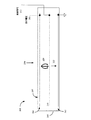
集束EBCCDにより、量子効率を維持または改良すると同時に、空間分解能、寿命、および信号対雑音比が改善された。図2は、集束EBCCD201の図である。EBCCD201は密封管205を含み、この密封管は、真空環境において感光性光電陰極204とCCD202を格納する。密封管205の上面はウィンドウ207を含む。ウィンドウ207は、対象の波長において透明である。UV感応性EBCCD検出器の場合、このウィンドウは、好ましくは、極めて純度の高いグレードの石英、溶融シリカ、またはアルミナ(サファイア)を含む。いくつかの好適な実施形態では、ウィンドウの外面はUV反射防止コーティングで被覆される。このコーティングは、低指数物質(例えばフッ化マグネシウム(MgF2))で作られた単層でもよく、あるいは多層コーティングでもよい。
Detailed Description of the Drawings Focused EBCCD has improved spatial resolution, lifetime, and signal-to-noise ratio while maintaining or improving quantum efficiency. FIG. 2 is a diagram of the focusing
光電陰極204は、ウィンドウ207に直接隣接して配置される。あるいは、ウィンドウ207のコーティングとして実装してもよい。光電陰極の材料は、光電子倍増管、イメージ増強管、またはCCD検出器用として当技術分野で公知の任意の光電陰極材料と実質的に同様であってよい。好適な実施形態では、光電陰極204は、1つ以上のアルカリ金属(例えばセシウム)を含んでよく、あるいは、半導体(例えば窒化ガリウム(GaN)、ヒ化ガリウム(GaAs))を含んでよい。光電陰極204は、CCD202に対して負の電圧203に保たれる。いくつかの実施形態では、負の電圧203は約1000Vであってよい。他の実施形態では、負の電圧203は数百ボルトまたは数十ボルトであってよい。
The
CCD202は、密封管205の底面近くに配置され、その背面に最初に電子が衝突する向きにされた薄化CCD(すなわち背面薄化CCD)である。背面薄化CCDは通常、例えば厚さ約500μmのシリコン基板の上面にトランジスタその他のデバイスを形成することにより形成される。ドーピングを用いて、p型、n型両方のデバイスを作製することができる。このようなデバイスは、厚さの異なる種々な材料で形成されるので、CCDに到達する電子の一部は、厚みのあるシリコンの他、これらのデバイスによっても遮断または吸収されることがある。したがって、電子が背面に衝突したときに可能な限り多くの電子を確実に検出できるようにするため、シリコンのかなりの部分が除去される。標準的な実施形態では、結果として得られるシリコンの厚さは25μm程度である。
The
不都合なことに、シリコンが露出していると、そこに天然酸化物が形成される。この天然酸化物は、電子がシリコンに進入するのを阻害することもある。したがって、一実施形態では、CCDを用いた検出の強化を促進する目的で、コーティングしなければ天然酸化物が堆積するシリコン露出部にホウ素コーティングを施すことができる。この保護コーティングについては、2012年6月12日に出願された米国特許仮出願第61/658,758号に詳述されている(この文献は、参照により本明細書に組み込まれる)。いくつかの実施形態では、CCD202は時間遅延積分(TDI)CCDである。いくつかの好適な実施形態では、CCD202は接地電位近くに保たれる。
Unfortunately, when silicon is exposed, natural oxide is formed there. This natural oxide may prevent electrons from entering the silicon. Thus, in one embodiment, for the purpose of promoting enhanced detection using a CCD, a boron coating can be applied to the exposed silicon where the native oxide is deposited without coating. This protective coating is described in detail in US Provisional Application No. 61 / 658,758, filed June 12, 2012, which is incorporated herein by reference. In some embodiments, the
集束を提供し、ゆえに性能を改善するため、EBCCD201はさらに、制御デバイス210を含む。制御デバイス210は1つ以上の制御信号212(例えば制御電圧)で制御される。一実施形態では、制御デバイス210は光電陰極204とCCD202の間に配置される。別の一実施形態では、制御デバイス210はCCD202に取り付けられる。
In order to provide focusing and thus improve performance,
制御デバイス210は、光電陰極204からCCD202に向けて進行する電子を有利に集束させて、電子の水平方向の広がりを最小化することができる。いくつかの実施形態では、制御デバイス210は、大きな水平速度成分を有する一部の電子を、集束でなく遮断することができる。この集束を提供するため、制御デバイス210は、貫通穴(すなわち開口)の配列を有する。一実施形態では、これらの穴のパターンはCCD202のピクセルのパターンと整列される。例えば、CCD202が20μm×20μmの正方形ピクセルを含む場合、制御デバイス210は、20μm×20μmのグリッド上に直径約10μmの穴の配列を含んでよい。いくつかの実施形態では、制御デバイス210の厚さは約25μm〜200μmであってよい。穴の配列とCCD202のピクセルの配列の整列を可能にするため、制御デバイス210は、整列機能をさらに含んでよい。同様に、制御デバイス210との整列を容易にするため、CCD202の片面または両面に整列マークを組み込んでもよい。
The
いくつかの実施形態では、制御デバイス210は金属板または金属箔を含んでよい。他の好適な実施形態では、制御デバイス210は、シリコン結晶またはシリコンウエハを含んでよい。制御デバイス210内の穴の製作は、レーザードリル加工(例えば金属製材料の場合)またはフォトリソグラフィとエッチング(例えば半導体材料の場合)により行ってよい。半導体技術を用いて制御デバイス210を製作する実施形態では、穴以外の要素を、制御デバイスの中および表面に形成することもできる。例えば、電極、ドーピング領域、電圧制御デバイス、および検出デバイスを、制御装置210の表面または中に形成してよい。
In some embodiments, the
上記の通り、マイクロチャンネルプレート(MCP)は二次電子を発生させ、この二次電子はデバイスの利得を増加させるが、デバイスの空間分解能を低下させる。対照的に、制御デバイス210は、電子の大部分をCCD202のピクセルに向けて集束させ、同時に、相当な水平速度成分を有する電子は遮断するか向きをそらす。いくつかの好適な実施形態では、光電陰極204と制御デバイス210上面の間の電位差が小さいので(例えば数ボルトまたは数十ボルト)、制御デバイス210の制御電極に実際に電子が衝突しても、二次電子はまったく発生しないか、ごく少数しか発生しない。
As described above, the microchannel plate (MCP) generates secondary electrons, which increase the gain of the device but reduce the spatial resolution of the device. In contrast, the
光230がEBCCD201に入射すると、1つ以上の電子220が光電陰極204から発せられる。これらの電子は実質的に全方向に放出され、光電陰極204と制御デバイス210間の電位差により、制御デバイス210に向かって加速する。制御デバイス210の穴により、電子は制御デバイス210内で実質的に平行にされる。したがって、制御デバイス210から現れた電子は、CCD202に対して実質的に垂直に進行する。これにより、所与の穴を通って進行する大部分の電子が、対応する(および整列された)CCD202のピクセルに確実に到着し、これにより画像ぶれが実質的に低減される。
When light 230 enters
図3Aは、代表的な制御デバイスにおける4つの穴310の上面図である。上記の通り、好ましくは、これらの穴は、CCDのピクセルのグリッドと一致するグリッド上に配置される。ただし、検出器が面検出器でなく線分検出器の場合、1列のみの穴を配置してよい。好適な実施形態では、穴の直径はCCDピクセルのサイズの約半分である。非限定的な例として、CCDのピクセルが20μm×20μmである場合、いくつかの実施形態では、個々の穴の直径は約10μmであり得る。いくつかの実施形態では、制御デバイスの厚さは、穴の直径の約2.5〜20倍の大きさである。例えば、CCDピクセルのサイズが約20μm×20μmである場合、穴の直径は約10μm、制御デバイスの厚さは約25μm〜約200μmであり得る。穴の直径より穴の長さの方がはるかに長いので、穴を通過する電子は、比較的狭い角度範囲で進行することになる。
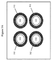
FIG. 3A is a top view of four
個々の穴310の周りを電極312が囲む。好適な実施形態では、穴310の内面は導電性であり、制御電圧に接続される。いくつかの実施形態では、(図2の電子220を表す矢印が示すように)穴310に向けて電子を引き付けるために、この電圧は光電陰極に対して正の電圧である。電子を穴310に向けるため、電極312は、穴310の内面とは異なる電圧にある。いくつかの実施形態では、電極312は、穴310の内面に対して負の電圧にある。いくつかの実施形態では、個々の穴310の周りに2つ以上の電極が設けられる。いくつかの実施形態では、制御デバイスの底面側の各穴の周りにも電極が設けられる。
An
図3Bは、制御デバイスの別の実施形態の図である。ここでは、個々の電極(例えば、図3Aに示す電極312)が統合されて、制御デバイス上面の大部分を覆う単一の電極322を形成している。いくつかの実施形態では、表面電極322と個々の穴310の間に小さなギャップ324が存在してよい。ギャップ324を形成するには、外側と内側で異なる電位を有する弱導電性要素を提供する不純物半導体(標準のドーパントを用いたn型またはp型のドーピング)を用いてよい。留意すべきことは、ギャップ324は絶縁体として形成されないことである。絶縁体として形成すると、電子を捕捉する傾向を有し、最終的に負に帯電するため、電子を穴310に引き付けるのでなく、電子を反発させることになる。
FIG. 3B is a diagram of another embodiment of a control device. Here, individual electrodes (eg,
図3Cは、制御デバイスのさらに別の実施形態の図である。この実施形態では、表面電極322と個々の穴310の間に内側電極332が設けられる。内側電極332と表面電極322は小さなギャップ330で分離される。一実施形態では、内側電極332と穴310を小さなギャップ324で分離してよい。好適な実施形態では、ギャップ324(および本明細書で論じる他のギャップ)ならびに制御デバイス表面の他の実質的に非導電性の領域を軽くドーピングするか、弱導電材料でコーティングすることにより、これらの表面にぶつかる電子またはイオンから表面が帯電するのを回避する。
FIG. 3C is a diagram of yet another embodiment of a control device. In this embodiment, an
図4Aは、線分検出器EBCCDでの使用に適した代表的な制御デバイスの上面図である。面検出器で使用する実質的に円形の穴の二次元配列の代わりに、実質的に長方形の穴410(またはスリット)の一次元配列を用いてよい。穴410の周りは、単一の表面電極412または複数の電極(図示せず)で囲まれる。個々の穴410と電極(単一または複数の電極)の間に小さなギャップ414を設けてよい。上述の通り、ギャップ414の材料を軽くドーピングして弱導電性にしてよく、これにより帯電が防止される。線分検出器のいくつかの実施形態では、穴410の幅は、CCDのピクセル幅の約半分である。これにより、線状配列に沿う方向の画像ぶれが最小化される。いくつかの実施形態では、穴410の縦の長さは、CCDのピクセルの縦の長さの約75%〜90%であり、これにより(線状配列の軸に対して垂直のぶれは重要性が低いので)電子の伝達が最大化される。
FIG. 4A is a top view of an exemplary control device suitable for use with line segment detector EBCCD. Instead of the two-dimensional array of substantially circular holes used in the surface detector, a one-dimensional array of substantially rectangular holes 410 (or slits) may be used. The
図4Bは、線分検出器EBCCDでの使用に適した別の代表的な制御デバイスの図である。この実施形態では、追加の電極420を個々の穴410の両側に配置するか、または穴の周りを囲む(図示せず)。
FIG. 4B is a diagram of another exemplary control device suitable for use with line segment detector EBCCD. In this embodiment,
理解すべきことは、上記の例は単なる実例として示すものであり、本発明の範囲を限定すると解釈すべきでないことである。多くの様々な電極構成、ギャップ構成、および穴構成が可能であることが認識されるであろう。例えば、一実施形態では、2を超える数の電極が個々の穴を囲み、あるいは個々の穴に隣接する。このように、電極、ギャップ、および穴の様々な構成が本発明の範囲内にある。 It should be understood that the above examples are given by way of illustration only and should not be construed to limit the scope of the invention. It will be appreciated that many different electrode configurations, gap configurations, and hole configurations are possible. For example, in one embodiment, more than two electrodes surround or are adjacent to an individual hole. Thus, various configurations of electrodes, gaps, and holes are within the scope of the present invention.
図4Cは、EBCCDの代表的実施形態の穴3個部分の断面図である。この実施形態では、光電陰極404は約−60Vの電位に保たれ、CCD402は約0Vの電位に保たれる。また、線分検出器の実施形態であると仮定すると、CCD402のピクセル幅が約18μmであるのに対し、ピクセルの縦の長さ(図4Cの平面に対して垂直の長さ)は、18μmより大きい(例えば約100μm以上である)。制御デバイス403は穴410(例えばスリット)の配列を含み、これらの穴はCCD402のピクセルと整列される。個々の穴410の幅は約9μm(すなわち、CCD402のピクセル幅の半分)である。この実施形態では、制御デバイス403の上端と光電陰極404の間のギャップは約10μmである。制御デバイスの厚さは約30μmである。この構成では、個々の穴410の上端の電位は実質的に−60Vである。特に注目すべきことは、穴410が光電陰極404の表面に対して垂直に形成されることである。これにより、穴410の側壁に衝突する電子の数が最少化され、その結果、二次電子の発生が最少化される。
FIG. 4C is a cross-sectional view of a three hole portion of an exemplary embodiment of an EBCCD. In this embodiment, the
制御デバイス403の一部分の詳細を、図4D(1)(上面図)と図4D(2)の断面図に示す。図4D(1)と4D(2)に示す通り、制御デバイス本体484において、第1電極412と第2電極446が内の個々の穴410を囲んでいる。穴410の幅と比べて、第1電極412および第2電極446の幅ははるかに狭い(例えば、少なくとも1:7程度)。第1電極と第2電極の間には、比較的大きなギャップ444が存在する。例えば、ピクセルサイズが約18μmの場合、ギャップの大きさは約4μmである。一実施形態では、ギャップ444は、微小導電性材料に露出してよい。例えば、領域482(全表面を図示)に示される通り、本体484の1つ以上の表面にドーピングまたは注入が施されてよい。あるいは、領域482は、本体484の表面に施された薄い抵抗性コーティングを含んでもよい。いくつかの実施形態では、電極412と446の間の本体484の表面のみ、ドーピング、注入、またはコーティングを施してよい。いくつかの実施形態では、電極412、446の一部または全部の下に微小導電性表面が広がるように(図4D(2)に図示)、先に本体484の表面にドーピング、注入、またはコーティングを施してから、電極412、446を付着させてよい。なお、本明細書に示す他の実施形態でも、電極の同様の実装を用いてよい。
Details of a portion of the
電極412、446は、導電性トレース(図示せず)により外部電圧に接続される。この導電性トレースは上面の真下にあってよい。代表的な一実施形態では、電極412、446は、光電陰極に対してわずかに負の電圧に保たれる。例えば、光電陰極が約−60Vの電位にあるとき、約−65Vに維持される。ギャップ444が導電性材料に露出しているので、第1電極と第2電極の間には、ほぼ線形の電圧勾配が存在する。代替の実施形態では、電極412と446の間で、電位の異なる追加の電極を使用してよい。これにより、所望の電圧勾配への段階的近似が実現可能になる。一実施形態では、制御デバイス403の底面に第3電極481を形成してよく、この電極は−5Vの電位を有してよい。
The
前の図4Cを参照すると、制御デバイス403の底面430は、導電性材料で形成された表面電極を含んでよく、CCD402に対して数ボルトだけ負の電圧に保持してよい。例えば、底面430を約−5Vの電圧に保持してよい。一実施形態では、底面430とCCD402の間のギャップは約20μmである。制御デバイス403の底面430とCCD402の間の電位差が小さいことの利点の1つは、CCD402の非平坦性が電子軌跡に与える影響がごく軽微であり、あるピクセルに対応する光電陰極404の領域から放出される電子のうち、CCD402の隣接ピクセルに到達する電子にはほとんど影響しないことである。一実施形態では、穴410の内面は、導電性材料(例えば不純物半導体、半金属材料等)を含む。上面と底面の間に電位差があるため、上面と底面の間の穴410の壁に沿って、ほぼ線形の電位勾配が生成される。
With reference to previous FIG. 4C, the
図4Cの線432は、上記の幾何学的配置と電圧に対してラプラスの方程式を解くことにより算出された、−59Vの等電位を表す。線434は、−4Vの等電位を表す。その他の等電位線(ラベル表示せず)は、−59V〜−4Vの電圧の5V間隔に対応する。
図4Eは、図4Cおよび4Dの代表的EBCCDの、光電陰極404から様々な方向に進行する電子に対して算出された電子軌跡を示す図である。各電子が約1eVのエネルギーで光電陰極から離れると仮定して、線451は、光電陰極404の1ピクセルの中心近くを離れる電子がたどる近似的な軌跡を示す。大部分の軌跡(例えば軌跡451)は、対応するCCDピクセルと整列した穴を用いてCCD402に到達する。少数の軌跡(例えば軌跡452)は隣の穴の方にそれるが、図示の通り、壁に当たる可能性が最も高い。少数(ラベル表示せず)は上面に到達する。少数(ラベル表示せず)は向きを変えて光電陰極402に戻る。図4Eに示す軌跡でCCD402の隣接ピクセルに到達する軌跡はほとんどないことから、制御デバイス403のない従来型EBCCDと比べて、この改良型EBCCDの分解能は(密な分布で示される通り)著しく優れている。その上、制御デバイス403または光電陰極404で停止する軌跡の数は、軌跡総数に対してごく少数であるため、このEBCCDは高効率である。
FIG. 4E is a diagram showing electron trajectories calculated for electrons traveling in various directions from the
図4Fは、別の代表的な制御デバイス460の断面図である。この実施形態では、制御デバイス460の上面の個々の穴410の間に畝462がある。この形状の違いを除き、このEBCCDの寸法は、図4Cおよび4Dに関して記載されている寸法と同様であってよい。畝462の上端は、光電陰極404から約5μmに位置してよい。このように距離が短いので、光電陰極に対する畝上端の電位差はわずか数ボルトでよく、例えば約−3Vでよい。畝462の利点の1つは、横向きに進行する電子を反射させる上で、正確な電圧がさほど重要でなくなることである。具体的には、制御デバイス460の上面が物理的に光電陰極404の近くに位置するので、上面の電圧が少し変化しても、電場勾配は、電子を反射するのに十分強力であることができる。この代表的な実施形態では、光電陰極404は約−60Vの電圧に保たれる。制御デバイス460の上面には、各畝の中心の約−63Vから、各穴410の端部近くの−60Vへの電圧勾配が存在する。制御デバイス460の底面の電圧は約0Vであり、CCD402は0Vの電圧にある。算出された等電位線464は約−59Vの等電位を表し、等電位線466は約−4Vを表す。その他の中間の等電位線は、約5Vきざみを表す。好適な一実施形態では、畝462の上端を妥当に一定の曲率半径で丸みを付けて、強力な電場勾配を最小化する。
FIG. 4F is a cross-sectional view of another
図4Gは、図4Fの代表的実施形態に対して算出された電子軌跡の一部を示す図である。線471は、光電陰極404から約1eVのエネルギーで様々な方向に発せられた電子に対して算出された軌跡を示す。この軌跡を図4Eの軌跡と比べると、図4Fの制御デバイス構成の方がCCD402に到達する電子の分布がコンパクトであり、ゆえに分解能の向上を示していることが分かる。
FIG. 4G is a diagram illustrating a portion of the electronic trajectory calculated for the exemplary embodiment of FIG. 4F. A
上記の実施形態では、光電陰極の電圧がCCDに対して約60V負電圧であるが、制御デバイスの集束効果は制御デバイスと光電陰極間の電位差に大きく依存することが理解されるであろう。いくつかの実施形態では、光電陰極は約500V、あるいは約1000Vといった大きな負の電圧にされ、光電陰極と制御デバイスの間の電圧差は数ボルト以内、または数十ボルト以内に維持されてよい。この場合、制御デバイスの底部とCCDの間に大きな電位差が存在し、これにより電子が高エネルギーへと加速してからCCDに衝突する。制御デバイスの底部とCCDの間に数百ボルト以上の電圧差が存在する場合、通常は、制御デバイスとCCDの間を数百ミクロン離すことが望ましい。数百ミクロン離すことにより、CCDの非平坦性がEBCCDの性能に及ぼす影響を低減することもできる。電子は、制御デバイスを離れるときに十分に平行にされるので、電子がより広範な角度で進行する従来型EBCCDの歪みと比べて、CCDの非平坦性から電場に生じる小さな歪みはさほど重要ではない。 In the above embodiment, the photocathode voltage is about 60V negative with respect to the CCD, but it will be understood that the focusing effect of the control device is highly dependent on the potential difference between the control device and the photocathode. In some embodiments, the photocathode may be at a large negative voltage, such as about 500V, or about 1000V, and the voltage difference between the photocathode and the control device may be maintained within a few volts, or within a few tens of volts. In this case, there is a large potential difference between the bottom of the control device and the CCD, which causes the electrons to accelerate to high energy before colliding with the CCD. If there is a voltage difference of several hundred volts or more between the bottom of the control device and the CCD, it is usually desirable to have a few hundred microns between the control device and the CCD. Separating several hundred microns can also reduce the effect of CCD non-flatness on the performance of EBCCD. Since the electrons are made sufficiently parallel as they leave the control device, the small distortion that occurs in the electric field due to CCD non-flatness is less important than the distortion of a conventional EBCCD where the electrons travel at a wider angle. Absent.
上記で示した通り、様々な制御デバイス形状と電圧分布により、EBCCDの操作性能を確実に改善することが可能である。したがって、制御デバイスを含む改良型EBCCDは、上記の制御デバイス形状と電圧分布に限定されるのでなく、他の制御デバイス形状と電圧分布も含み得る。図4A〜4Gは線形EBCCD検出器の代表的実施形態を示しているが、これらの代表的構成を、二次元EBCCD配列の検出器に応用することができる。 As indicated above, various control device shapes and voltage distributions can reliably improve the operating performance of the EBCCD. Thus, an improved EBCCD including a control device is not limited to the control device shape and voltage distribution described above, but may include other control device shapes and voltage distributions. 4A-4G illustrate exemplary embodiments of linear EBCCD detectors, these exemplary configurations can be applied to detectors in a two-dimensional EBCCD array.
留意すべきことは、金属製制御デバイスでなく、シリコンMEMSデバイスを用いて制御デバイスを実装した方が、いくつかの利点を得られることである。具体的には、どちらの実施形態も、穴の配列を通過する電子を平行にさせることにより、従来のEBCCD検出器と比べて空間分解能を実質的に改善できるが、金属製制御デバイスは、水平方向速度成分が比較的大きく、これらの電子を吸収することがある。これにより、シリコンMEMS制御デバイスを含むEBCCDと比べて効率が低下する。シリコンMEMS制御デバイスの場合、その電極構造と、各電極での適切な電圧の使用により、大部分の電子を穴に向けることができ、よって一段と多くの電子をCCDに搬送することができる。 It should be noted that implementing the control device using a silicon MEMS device rather than a metal control device provides several advantages. Specifically, both embodiments can substantially improve the spatial resolution compared to conventional EBCCD detectors by collimating electrons passing through the array of holes, but the metal control device is The direction velocity component is relatively large and may absorb these electrons. This reduces the efficiency compared to EBCCD including a silicon MEMS control device. In the case of a silicon MEMS control device, most of the electrons can be directed to the hole by means of its electrode structure and the use of appropriate voltages at each electrode, so that more electrons can be transported to the CCD.
いくつかの実施形態では、制御デバイスを制御する1つ以上の制御電圧を調整して、EBCCDの利得を変化させることができる。原理上は、光電陰極の電圧を調整することでEBCCDの利得を変えることが可能であるが、光電陰極の静電容量が大きいため、光電陰極の電圧を迅速に変化させるには、大電流が必要になると考えられる。制御デバイスの穴および/または1つ以上の電極の電圧を変えることにより、CCDに到達する電子の一部を減少させて、EBCCDの実効利得を低下させることが可能である。いくつかの実施形態では、この利得低下は、光電陰極の電圧を変える場合より低い駆動電流で実施できる。いくつかの実施形態では、標準の半導体製造手法を用いて、MEMSデバイス上にトランジスタ、ダイオード、抵抗器等の能動回路を製作する。これらの能動回路により、電極電圧の局所制御が可能になり、このような電圧をより迅速に変更できるようになる。いくつかの実施形態では、EBCCDの様々な領域が様々な利得を有するように、上記の能動回路を用いて制御デバイスの様々なセクションの利得を変更する。いくつかの実施形態では、個々のピクセルまたはピクセル群の利得またはブランキングを制御することができる。 In some embodiments, one or more control voltages that control the control device can be adjusted to change the gain of the EBCCD. In principle, it is possible to change the gain of EBCCD by adjusting the voltage of the photocathode, but since the capacitance of the photocathode is large, a large current is required to change the photocathode voltage quickly. It is considered necessary. By changing the voltage on the hole in the control device and / or one or more electrodes, it is possible to reduce some of the electrons reaching the CCD and thus reduce the effective gain of the EBCCD. In some embodiments, this gain reduction can be performed with a lower drive current than when changing the photocathode voltage. In some embodiments, active circuits such as transistors, diodes, resistors, etc. are fabricated on MEMS devices using standard semiconductor manufacturing techniques. These active circuits allow local control of the electrode voltage and allow such voltages to be changed more quickly. In some embodiments, the active circuit described above is used to change the gain of the various sections of the control device so that different regions of the EBCCD have different gains. In some embodiments, the gain or blanking of individual pixels or groups of pixels can be controlled.
いくつかの実施形態では、制御デバイス下面とCCDの間の電位差は小さい(例えば20V以下)か、または実質的にゼロであってよい。制御デバイスの底部とCCDの間に弱電場が存在するか電場がまったく存在しなければ、CCDの非平坦性が原因で、画像が著しく歪んだり、利得が局所的に著しく変動したりすることがなくなる。 In some embodiments, the potential difference between the lower surface of the control device and the CCD may be small (eg, 20V or less) or substantially zero. If there is a weak electric field or no electric field between the bottom of the control device and the CCD, the non-flatness of the CCD may cause the image to be distorted and the gain to be significantly fluctuated locally. Disappear.
いくつかの実施形態では、カスケード状に配置された2つの制御デバイスを用いてよい。この場合、第1制御デバイスの電位は、光電陰極の電位から10ボルト以内または数十ボルト以内の範囲にあり、下流の第2制御デバイスは、CCDに近い電位(例えばCCDに対して−20V)にある。第1および第2制御デバイスの間に大きな電位差が存在してよい(例えば数十ボルト、数百ボルト、あるいは約1000Vも可)。この構成では、光電陰極から発せられた電子を第1制御デバイスが集束して、平行にするのに対し、第2制御デバイスは、平行にされた電子を加速する。 In some embodiments, two control devices arranged in cascade may be used. In this case, the potential of the first control device is within a range of 10 volts or several tens of volts from the potential of the photocathode, and the downstream second control device has a potential close to the CCD (for example, −20 V with respect to the CCD). It is in. There may be a large potential difference between the first and second control devices (eg, tens of volts, hundreds of volts, or about 1000 volts). In this configuration, the first control device focuses and collimates the electrons emitted from the photocathode, while the second control device accelerates the collimated electrons.
いくつかの実施形態では、制御デバイスとCCDの間の整列を、CCDピクセルサイズの少なくとも約20%の精度で実施することが所望され得る。EBCCDの組み立て時に制御デバイスとCCDの両方をシリコン上に製作する実施形態では、波長約1.2μm超の赤外線を使用して、2つのシリコンデバイス上の整列マークを検出することができる(この赤外線であればシリコンを貫通できるため)。CCDの底面(実際には、背面薄化工程前のCCD製造中はウエハの上面)上の整列マークまたは回路特徴物と、シリコンMEMS制御デバイス上のマークを一致させることができ、これにより双方を確実に所望の精度に整列させることができる。 In some embodiments, it may be desirable to perform alignment between the control device and the CCD with an accuracy of at least about 20% of the CCD pixel size. In an embodiment in which both the control device and the CCD are fabricated on silicon during the assembly of the EBCCD, an infrared mark with a wavelength greater than about 1.2 μm can be used to detect alignment marks on the two silicon devices (this infrared If so, it can penetrate silicon). Alignment marks or circuit features on the bottom surface of the CCD (actually the top surface of the wafer during CCD manufacturing prior to the backside thinning process) can be aligned with the marks on the silicon MEMS control device. It can be surely aligned to a desired accuracy.
上記の制御デバイスは、電子を有利に平行にすることができるので、画像ぶれが減少する。画像ぶれが減ることから、いくつかの実施形態では、光電陰極に必要とされる負電圧の度合いが減少する。その上、制御デバイスは、CCDから光電陰極に戻って来るイオンの大部分を遮断することもできるので、光電陰極の摩耗率が低下する。さらに、イオンが実際に光電陰極に到達しても、そのエネルギーは比較的低く、材料の消耗が比較的少ないので、検出器の耐用寿命が長期化する。さらに、制御デバイスから放出される電子は(制御デバイスがない場合と比べて)低エネルギーでCCDに衝突するので、CCDに与える損傷が少なくなる。その上、このような電子であれば、CCDからの物質のスパッタリングが減少するので、結果として生じるイオンが減り、検出器の寿命がさらに長期化する。 The control device described above can advantageously collimate the electrons, reducing image blur. Because image blur is reduced, in some embodiments, the degree of negative voltage required for the photocathode is reduced. Moreover, the control device can also block most of the ions returning from the CCD to the photocathode, reducing the photocathode wear rate. Furthermore, even if ions actually reach the photocathode, the energy is relatively low and the material consumption is relatively low, which extends the useful life of the detector. Furthermore, the electrons emitted from the control device collide with the CCD with low energy (as compared to the case without the control device), so that damage to the CCD is reduced. Moreover, such electrons reduce the sputtering of the material from the CCD, resulting in fewer ions and further extending the lifetime of the detector.
以下に詳述する通り、ウエハ、レチクル、およびフォトマスクの検査システムに、制御デバイスを有するEBCCDを有利に含めることができる。散乱光レベルは表面粗さおよび表面上の粒子または欠陥のサイズに依存するので、制御デバイスを有するEBCCDの利得制御を有利に使用して、様々な散乱光レベルを補正することができる。 As detailed below, the wafer, reticle, and photomask inspection systems may advantageously include an EBCCD having a control device. Since the scattered light level depends on the surface roughness and the size of the particles or defects on the surface, the gain control of the EBCCD with the control device can be advantageously used to correct various scattered light levels.
図5は、反射屈折イメージングシステム500に垂直入射レーザー暗視野照明を追加した図である。この暗視野照明は、UVレーザー501と、照射ビームサイズおよび検査面プロファイルを制御するための適応光学系502と、機械収容部504内の開口およびウィンドウ503と、光軸に沿って法線入射するレーザーの方向をサンプル508の表面に向け直すためのプリズム505と、を含む。また、プリズム505は、サンプル508の表面形状からの鏡面反射と、対物レンズ506の光学的表面からの光路に沿った反射を、イメージ平面(または検出器)アレイ509の方向に向ける。対物レンズ506用のレンズは、反射屈折対物レンズ、集束レンズ群、およびズームチューブレンズの一般的形態で提供してよい。好適な一実施形態では、暗視野散乱信号が弱信号であり得ることから、制御デバイスを有する上記EBCCD検出器を用いて、イメージ平面(または検出器)アレイ509を有利に実装することができる。上記の制御デバイスを有するEBCCDは、この応用によく適している。その理由は、EBCCDの空間分解能が高いからであり、いくつかの実施形態では、検査対象ウエハ上のパターンに応じて変化する散乱光レベルに応答して、またはこれを見越して、EBCCDの利得を制御できるからである。2007年1月4日に公開された米国特許出願公開第2007/0002465号に、システム500のいくつかの態様がさらに詳しく記載されており、この文献は参照により本明細書に組み込まれる。
FIG. 5 is a diagram in which normal incidence laser dark field illumination is added to the
図6Aは、別の表面検査装置600の図である。この検査装置は、表面領域611を検査するための照明システム601と収集システム610を含む。図6Aが示す通り、レーザーシステム615は、光ビーム602がレンズ603を通過する方向に向くように構成される。レンズ603は、その平面が表面611と実質的に平行になる向きにされ、その結果、表面611上のレンズ603の焦点面に照明線(illumination line)605が形成される。加えて、光ビーム602と集束ビーム604は、非直行入射角で表面611に向かうように方向付けされる。特に、光ビーム602と集束ビーム604は、表面611に対する法線方向から約1度〜約85度の角度で方向付けされてよい。このようにして、照明線605は、実質的に集束ビーム604の入射面の中にある。いくつかの実施形態では、照明線の長さは約1mm、2mm、または数mm、幅は1μm、2μm、または数μmであり得る。いくつかの実施形態では、線状焦点の代わりに、照明を一連の個別の点に集束させてもよい。
FIG. 6A is a diagram of another
収集システム610は、照明線605からの散乱光を収集するためのレンズ612と、レンズ612から入射した光をデバイス(例えば、上記制御デバイスを含むEBCCD検出器614)上に集束させるためのレンズ613を含む。この種の検査システムでは、EBCCD検出器614の利得を動的に調整することが重要である。その理由は、ウエハのパターンが多様であることに起因して、ウエハの領域によって散乱光レベルと回折光レベル(およびフィルタ効率)が劇的に変わることがあるからである。
The
一実施形態では、EBCCD検出器614は、線状配列の複数の検出器を含んでよい。この場合、EBCCD検出器614内の線状配列の検出器を、照明線615と平行する向きにしてよい。一実施形態では、多重収集システムを含めることできる。この場合、各収集システムは、類似しているが向きの異なる構成要素を含む。例として、図6Bに、表面検査装置用の収集システム621、622、623の代表的配列を示す(この図は、簡単にするために、例えば照明システム601と同様の照明システムを表示していない)。2009年4月8日に発行された米国特許第7,525,649号に、検査システム601のいくつかの態様がさらに詳しく記載されており、この文献は参照により本明細書に組み込まれる。
In one embodiment,
図7は、表面701上の異常の検査に使用できる表面検査システム700の図である。この実施形態では、システム700の実質的に固定された照明デバイス部分で表面701を照らすことができる。この照明デバイス部分は、レーザーシステム720により生成されたレーザービームを含む。レーザーシステム720の出力は、偏光光学系721、ビーム拡大器と開口722、およびビームを拡大し集束させるためのビーム形成光学系723を連続的に通過することができる。
FIG. 7 is a diagram of a
次に、集束したレーザービーム702がビーム折り曲げ(ターニング)部品703とビーム偏向器704に反射され、ビーム705が表面701の方向に向けられて、表面を照らす。好適な実施形態では、ビーム705は表面701に対して実質的に法線すなわち垂直であるが、他の実施形態では、ビーム705は表面701に対して斜角であってよい。
Next, the
一実施形態では、ビーム705は表面701に対して実質的に垂直すなわち法線であり、ビーム偏向器704は、表面701からのビームの鏡面反射をビーム折り曲げ部品703に向けて反射させる。これにより、ビーム偏向器は、鏡面反射が検出器に到達するのを防ぐシールドの働きをする。鏡面反射の方向は、表面701に対して法線をなす線SRに沿っている。ビーム705が表面701に対して法線をなす一実施形態では、この線SRは、照明ビーム705の方向と一致する。この共通の基準線または方向を、本明細書では検査システム700の軸と称する。ビーム705が表面701に対して斜角である場合、鏡面反射SRの方向とビーム705の入射方向は一致しない。この場合、表面法線の方向を示すSR線を、検査システム700の収集部分の主軸と称する。
In one embodiment, the
小粒子により散乱した光はミラー706により収集され、開口707および検出器708の方に送られる。大型粒子により散乱した光はレンズ709により収集され、開口710および検出器711の方に送られる。留意すべきことは、大型粒子の一部から散乱する光は、収集されて検出器708にも送られ、同様に、小型粒子の一部から散乱する光は、収集されて検出器711にも送られるが、このような光は、各検出器が検出するように設計される散乱光と比べて、散乱光強度が相対的に低いことである。一実施形態では、パターン無しウエハ上の欠陥検出用として検査システムを構成してよい。一実施形態では、検出器708、711の1つ以上を、上記制御デバイスを有するEBCCDにより実装することができる。2001年8月7日に発行された米国特許第6,271,916号に、検査システム700のいくつかの態様がさらに詳しく記載されており、この文献は参照により本明細書に組み込まれる。
Light scattered by the small particles is collected by
図8は、法線、傾斜両方の照明ビームを用いて異常検出を実装するように構成された暗視野検査システム800の図である。この実施形態では、レーザーシステムからレーザービーム801を供給できる。レンズ802が空間フィルタ803を通じてビーム801を集束させ、レンズ804がビームを平行にして、偏光ビームスプリッタ805に伝送する。ビームスプリッタ805は、第1偏光成分を法線照明チャンネルに渡し、第2偏光成分を傾斜照明チャンネルに渡す。ここで、第1成分と第2成分は直交する関係にある。法線照明チャンネル806では、第1偏光成分が光学系807により集束され、ミラー808に反射されて、サンプル809の表面に向かう。サンプル809により散乱した放射線は、放物面ミラー810により収集、集束され、光電子倍増管811に送られる。
FIG. 8 is a diagram of a dark
傾斜照明チャンネル812では、第2偏光成分がビームスプリッタ805に反射されてミラー813に送られ、このミラーで反射したビームが半波長板814を通過し、光学系815により集束され、サンプル809に送られる。傾斜チャンネル812の傾斜照明ビームから生じサンプル809により散乱する放射線は、放物面ミラー810により収集、集束され、検出器811に送られる。一実施形態では、検出器811を、上記制御デバイスを有するEBCCDにより実装することができる。好ましくは、検出器および照射スポット(法線照射チャンネルと傾斜照射チャンネルから表面809に照射されるスポット)は、放物線ミラー810の焦点位置にある。
In the tilted
放物線ミラー810は、サンプル809からの散乱放射線を平行にして、平行ビーム816にする。次に、平行ビーム816は対物レンズ817により集束され、分析器818を通って検出器811に到達する。なお、放物面以外の形状を有するカーブミラー面を使用してもよい。器具820がビームとサンプル809の間の相対運動を提供できるので、サンプル809表面全体に渡って照射スポットが走査される。一実施形態では、EBCCD検出器811からの出力をコンピュータ830が受信できる。2001年3月13日に発行された米国特許第6,201,601号に、検査システム800のいくつかの態様が記載されており、この文献は参照により本明細書に組み込まれる。
図9は、複数のEBCCD検出器を含む別の暗視野ウエハ検査システム900の図である。システム900では、光源901が発した光ビームを照明光学系902が受け取る。一実施形態では、照明光学系902の中に、複数のビームスプリッタと、屈折光学要素に実質的に平行な出力光ビームを提供する複数の反射光学要素とが含まれていてよい。この場合、続いて屈折光学要素が複数の光ビームをサンプル903に集束させることができる。
FIG. 9 is a diagram of another dark field wafer inspection system 900 that includes a plurality of EBCCD detectors. In the system 900, the illumination
光学収集サブシステム907は、散乱光収集器その他の要素(例えば、1つ以上の開口、スプリッタ、偏光要素、反射光学要素)を含み、サンプルからの散乱光を2つのイメージ検出器906に向けることができる。一実施形態では、光学収集サブシステム907は、屈折光学要素905をさらに含んでよい。屈折光学要素905は、光学収集サブシステム907の他の要素が散乱光をイメージ検出器906に向けて画像化するのを援助するように構成される。一実施形態では、イメージ検出器906の少なくとも一方は、制御デバイスを含む上記のEBCCD検出器を含むことができる。例えば、一実施形態では、一方の検出器を実質的な光散乱用に最適化し、別の検出器を実質的に低い光散乱用に最適化してよい。したがって、走査の一部の間、散乱光の一部分は実質的光散乱用に最適化された一方のイメージ検出器に向けられ、散乱光の別の部分は低光散乱用に最適化された別のイメージ検出器に向けられるように、光学要素を構成してよい。2011年7月12日に出願された米国特許仮出願第61/506,892号の優先権を主張している2012年7月9日に出願された米国特許出願第13/544,954号に、より詳細にシステム900のいくつかの態様が記載されている。この2つの特許出願は、参照により本明細書に組み込まれる。
The optical collection subsystem 907 includes scattered light collectors and other elements (eg, one or more apertures, splitters, polarizing elements, reflective optical elements) and directs scattered light from the sample to the two
図10は、連続移動物体1001(例えばウエハ、マスク、レチクル)を伴うパルス照明源1006を使用するように構成された代表的な検査/測定システム1000の図である。有利には、パルス照明1006は長パルスを出力することができる。パルス照明1006の代表的な光源は、Qスイッチレーザーまたはパルスランプを含むことができる。Qスイッチレーザーは、レーザーの光発振器内部の可変減衰器を使用して、極度に高いピーク出力で光パルスを生成する。この光パルスは、連続モードで作動する同一レーザーが生成する光パルスと比べて、出力がはるかに高い。パルスランプは、遠紫外線(DUV)エキシマーまたは超紫外線(EVU)源により実装可能である。好適な一実施形態では、パルス幅は、実施する時間遅延積分(TDI)のライン周期(line period)に近いか、ライン周期より多少長い。
FIG. 10 is a diagram of an exemplary inspection /
システム1000では、ビームスプリッタ1007がパルス照明源1006からの照明パルスを対物レンズ1004の方向に向け、この対物レンズが光を物体1001へと集束させる。次に、物体1001からの反射光がイメージセンサ1010の方向に向けられる。一実施形態では、上記のEBCCDの実施形態のいずれかを用いてイメージセンサ1010を実装することができる。なお、光の方向付けと集束を行う他の周知の光学部品は、簡単にするため図10には表示していない。イメージセンサ1010に連結されたプロセッサ1020は、パルス照明源1006からの照明パルスと、イメージセンサ1010との間でやり取りする制御信号およびデータ信号とを同期させ、さらにイメージデータを分析するように構成される。上記の構成では、物体1001は物体運動1003を有し、イメージセンサ1010上のイメージはイメージ運動1009を有する。
In
システム1000の一態様によれば、物体運動1003があるので、図の照明領域1002a(例えば時間帯N)、前の照明領域1002b(例えば時間帯N−1)、前の照明領域1002c(例えば時間帯N−2)で示されるように、照明領域は物体1001を横切って連続的に移動する。各照明領域1002a、1002b、1002cは、細長い長方形の領域であってよい(見やすくするため縮尺通りに表示していない)。留意すべきことは、明確にするため領域を分離して図示しているが、画像化範囲を100%確保し、あるいは欠陥検出中に追加的な冗長性と性能を得る目的で、領域が部分的に重なってよいことである。
According to one aspect of the
システム1000の別の態様によれば、イメージセンサ1010は、照明パルス中にTDIモード動作を実行できる。このTDIモード動作中、イメージセンサのピクセルにより保存された電荷は第1方向にのみ移動する。システム1000は、非照明中に分割読み出し動作も実行することができる。この分割読み出し動作中、イメージセンサの第1ピクセルにより保存された第1電荷は第1方向に移動し、イメージセンサの第2ピクセルにより保存された第2電荷は同時に第2方向に移動する。この第2方向は第1方向と反対方向にある。
According to another aspect of the
このように、システム1000は、TDI読み出しモードの有益な特性と、パルスイメージアーキテクチャの高速読み出し能力とを有利に組み合わせることができる。システム1000の他の態様については、2012年12月10日に出願された米国特許出願第61/735,427号(名称「Method And Apparatus For High Speed Acquisition Of Moving Images Using Pulsed Illumination」)により詳細に記載されており、この文献は参照により本明細書に組み込まれる。
Thus, the
本発明の例示的実施形態を添付の図を参照しながら本明細書で詳細に記載したが、本発明は、これらの厳密な実施形態に限定されないものと理解される。上記の実施形態は、網羅的であるという意図はなく、開示される厳密な形態に本発明を限定するという意図もない。したがって、当業者には多くの修正および変形が明らかになるであろう。例えば、上記実施形態では制御デバイス内に円形の穴を表示しているが、他の実施形態では、楕円形や長方形の穴でよい。概して、この穴の形状とサイズは、CCDの対応する(そして整列される)ピクセルの形状とサイズに基づく。穴のコーナーが尖っていると電場勾配が増加し得るが、このことは、CCDが二次元ピクセル配列である用途には望ましくないと考えられる。しかし、CCDが一次元ピクセル配列である用途では、端のピクセルに衝突する電子は比較的少数となる。コーナーに衝突する電子が少なくなるので、望ましくない電場勾配に電子が遭遇する確率は最小になる。結果として、このような実施形態では、尖ったコーナーは容認可能となり得る。また、上記の通り、半導体技術を用いて制御デバイスを製作する場合には、制御デバイス内に電圧制御デバイスおよび/または検出デバイスを形成してよい。いくつかの実施形態では、電子軌跡に与える影響を最小にする目的で、これらのデバイスを、制御デバイス内でなく制御デバイスの底面(すなわちCCDに面する側)に形成してよい。いくつかの実施形態では、電子検出器は、CCDでなくCMOSイメージセンサを含んでよい。したがって、本発明の範囲は、以下の請求項およびその均等物により定義されることが意図される。 While exemplary embodiments of the present invention have been described in detail herein with reference to the accompanying drawings, it is understood that the present invention is not limited to these exact embodiments. The above embodiments are not intended to be exhaustive and are not intended to limit the invention to the precise forms disclosed. Accordingly, many modifications and variations will be apparent to practitioners skilled in this art. For example, in the above embodiment, a circular hole is displayed in the control device, but in other embodiments, an elliptical or rectangular hole may be used. In general, the shape and size of this hole is based on the shape and size of the corresponding (and aligned) pixels of the CCD. Sharp hole corners can increase the electric field gradient, which is considered undesirable for applications where the CCD is a two-dimensional pixel array. However, in applications where the CCD is a one-dimensional pixel array, a relatively small number of electrons strike the end pixels. Since fewer electrons impact the corners, the probability that the electrons will encounter an undesirable electric field gradient is minimized. As a result, in such an embodiment, a sharp corner may be acceptable. Further, as described above, when a control device is manufactured using semiconductor technology, a voltage control device and / or a detection device may be formed in the control device. In some embodiments, these devices may be formed on the bottom surface of the control device (i.e., the side facing the CCD) rather than in the control device in order to minimize the impact on the electron trajectory. In some embodiments, the electronic detector may include a CMOS image sensor instead of a CCD. Accordingly, the scope of the invention is intended to be defined by the following claims and their equivalents.
Claims (25)
前記アセンブリの内側にあり、かつ前記ウィンドウに隣接する光電陰極と;
前記アセンブリの内側にあり、かつ前記光電陰極から発せられた電子を収集するように位置付けられた電荷結合素子(CCD)デバイスと;
前記光電陰極と前記CCDの間に位置付けられ、内部に複数の穴を有する制御デバイスと;
を含む、電子衝撃電荷結合素子(EBCCD)であって、
前記複数の穴は、前記光電陰極の表面に対して垂直に形成され、前記複数の穴のパターンは前記CCDにおけるピクセルのパターンと整列され、各穴は、前記制御デバイスの前記光電陰極に面する表面に形成された少なくとも1つの第1電極に囲まれる、
電子衝撃電荷結合素子(EBCCD)。 An assembly including a window;
A photocathode inside the assembly and adjacent to the window;
A charge coupled device (CCD) device located inside the assembly and positioned to collect electrons emitted from the photocathode;
A control device positioned between the photocathode and the CCD and having a plurality of holes therein;
An electron impact charge coupled device (EBCCD) comprising:
The plurality of holes are formed perpendicular to the surface of the photocathode, the pattern of the plurality of holes is aligned with a pattern of pixels in the CCD, and each hole faces the photocathode of the control device. Surrounded by at least one first electrode formed on the surface;
Electron impact charge coupled device (EBCCD).
前記EBCCDの光電陰極を前記EBCCDのCCDに対して負の電圧に保つことと;
前記光電陰極とCCDとの間に配置された制御デバイス内に形成された複数の穴に電子を通過させることにより、前記光電陰極から前記CCDのピクセルに向かって進行する電子を集束させることであって、前記複数の穴を光陰極の表面に対し垂直に形成することで前記CCDに対し垂直に伝播する前記電子の前記複数の穴の側壁の影響を小さくすること;
を含み、
前記電子を集束させることは、前記制御デバイスの前記複数の穴の各穴をCCDの1つの対応するピクセルと位置合わせさせて、各ホールを通過する大部分の電子が対応するピクセル上に着地させることをさらに含む、方法。 A method of operating an electron impact charge coupled device (EBCCD) comprising:
And keeping the negative voltage photocathode of the EBCCD respect CCD before Symbol E BCCD;
The electrons traveling from the photocathode to the CCD pixel are focused by passing electrons through a plurality of holes formed in a control device disposed between the photocathode and the CCD. Reducing the influence of the side walls of the plurality of holes propagating perpendicularly to the CCD by forming the plurality of holes perpendicular to the surface of the photocathode;
Including
Focusing the electrons aligns each hole of the plurality of holes of the control device with one corresponding pixel of the CCD so that the majority of electrons passing through each hole land on the corresponding pixel. The method further comprising:
前記サンプルからの散乱光を収集し、収集した光を方向付けるための光学系と;
前記収集した光を受け取るための電子衝撃電荷結合素子(EBCCD)検出器と;
を含む、暗視野検査システムであって、
前記EBCCD検出器は、
ウィンドウを含むアセンブリと;
前記アセンブリの内側にあり、かつ前記ウィンドウに隣接する光電陰極と;
前記アセンブリの内側にあり、かつ前記光電陰極から発せられた電子を収集するように位置付けられたCCDデバイスと;
前記光電陰極と前記CCDの間に位置付けられ、内部に複数の穴を有する制御デバイスと;を含み、
前記複数の穴は、前記光電陰極の表面に対して垂直に形成され、前記複数の穴のパターンは前記CCDにおけるピクセルのパターンと整列され、各穴は、前記制御デバイスの前記光電陰極に面する表面に形成された少なくとも1つの第1電極に囲まれる、
暗視野検査システム。 An optical system for directing light to the sample to be examined;
An optical system for collecting scattered light from the sample and directing the collected light;
An electron impact charge coupled device (EBCCD) detector for receiving the collected light;
A dark field inspection system comprising:
The EBCCD detector is
An assembly including a window;
A photocathode inside the assembly and adjacent to the window;
A CCD device inside the assembly and positioned to collect electrons emitted from the photocathode;
A control device positioned between the photocathode and the CCD and having a plurality of holes therein;
The plurality of holes are formed perpendicular to the surface of the photocathode, the pattern of the plurality of holes is aligned with a pattern of pixels in the CCD, and each hole faces the photocathode of the control device. Surrounded by at least one first electrode formed on the surface;
Dark field inspection system.
前記ウエハの領域に光を当てることと;
前記ウエハからの散乱光を収集することと;
収集した光を電子衝撃電荷結合素子(EBCCD)検出器へと方向付けることと;
を含み、前記EBCCD検出器は、
前記EBCCDの光電陰極を前記EBCCDのCCDに対して負の電圧に保つことであって、前記CCDはパターンで配置された複数のピクセルを含むことと;
前記光電陰極とCCDとの間に配置された制御デバイス内に形成された複数の穴に電子を通過させることにより、前記光電陰極から前記CCDのピクセルに向かって進行する電子を集束させることであって、前記複数の穴を光陰極の表面に対し垂直に形成することで前記CCDに対し垂直に伝播する前記電子の前記複数の穴の側壁の影響を小さくすること;
を含み、
前記複数の穴が前記パターン内に配置され、前記制御デバイスは、前記複数の穴の各穴をCCDの1つの対応するピクセルと位置合わせさせて、各ホールを通過する大部分の電子が前記ピクセルのパターンの前記対応するピクセル上に着地するように位置決めされている、検査方法。 A method for inspecting a semiconductor wafer,
Illuminating the area of the wafer;
Collecting scattered light from the wafer;
Directing the collected light to an electron impact charge coupled device (EBCCD) detector;
The EBCCD detector includes:
Maintaining the EBCCD photocathode at a negative voltage relative to the EBCCD CCD, the CCD comprising a plurality of pixels arranged in a pattern;
The electrons traveling from the photocathode to the CCD pixel are focused by passing electrons through a plurality of holes formed in a control device disposed between the photocathode and the CCD. Te, to reduce the effect of side walls of said plurality of holes of the electrons propagating perpendicular to the CCD by vertically forming the plurality of holes to the surface of the photocathode that;
Including
The plurality of holes are arranged in the pattern, and the control device aligns each hole of the plurality of holes with one corresponding pixel of the CCD so that most of the electrons passing through each hole are in the pixel. The inspection method is positioned to land on the corresponding pixel of the pattern.
前記検査システムは、パルス照明光源と;
電子衝撃電荷結合素子(EBCCD)検出器を含むイメージセンサと、を含み;
前記EBCCD検出器は、
ウィンドウを含むアセンブリと;
前記アセンブリの内側にあり、かつ前記ウィンドウに隣接する光電陰極と;
前記アセンブリの内側にあり、かつ前記光電陰極から発せられた電子を収集するように位置付けられたCCDと;
前記光電陰極と前記CCDの間に位置付けられ、内部に複数の穴を有する制御デバイスと;を含み、
前記複数の穴は、前記光電陰極の表面に対して垂直に形成され、前記複数の穴のパターンは前記CCDにおけるピクセルのパターンと整列され、各穴は、前記制御デバイスの前記光電陰極に面する表面に形成された少なくとも1つの第1電極に囲まれており;
前記検査システムは、
前記パルス照明光源からのパルス照明を連続移動物体へと方向付けるように、かつ前記物体からの反射光を前記イメージセンサへと方向付けるように構成された光学構成要素と;
前記イメージセンサを操作するように構成されたプロセッサと;を含み、
処理を行う構成は、
照明パルス中に時間遅延積分(TDI)操作を行うことであって、TDI操作中、前記イメージセンサのピクセルにより保存された電荷は第1方向にのみ移動することと;
非照明中に分割読み出し操作を行うことであって、前記分割読み出し中、前記イメージセンサの第1ピクセルにより保存された第1電荷は前記第1方向に移動し、前記イメージセンサの第2ピクセルにより保存された第2電荷は第2方向に同時に移動し、前記第2方向は前記第1方向と反対方向にあることと、を含む、
検査システム。 An inspection system,
The inspection system comprises a pulsed illumination light source;
An image sensor including an electron impact charge coupled device (EBCCD) detector;
The EBCCD detector is
An assembly including a window;
A photocathode inside the assembly and adjacent to the window;
A CCD located inside the assembly and positioned to collect electrons emitted from the photocathode;
A control device positioned between the photocathode and the CCD and having a plurality of holes therein;
The plurality of holes are formed perpendicular to the surface of the photocathode, the pattern of the plurality of holes is aligned with a pattern of pixels in the CCD, and each hole faces the photocathode of the control device. Surrounded by at least one first electrode formed on the surface;
The inspection system includes:
An optical component configured to direct pulse illumination from the pulse illumination light source to a continuously moving object and to direct reflected light from the object to the image sensor;
A processor configured to operate the image sensor;
The configuration to process is
Performing a time delay integration (TDI) operation during the illumination pulse, wherein during the TDI operation, the charge stored by the pixels of the image sensor moves only in a first direction;
Performing a divided read operation during non-illumination, wherein during the divided read, the first charge stored by the first pixel of the image sensor moves in the first direction and is moved by the second pixel of the image sensor. The stored second charge moves simultaneously in a second direction, and the second direction is opposite to the first direction,
Inspection system.
Applications Claiming Priority (5)
| Application Number | Priority Date | Filing Date | Title |
|---|---|---|---|
| US201161569611P | 2011-12-12 | 2011-12-12 | |
| US61/569,611 | 2011-12-12 | ||
| US13/710,315 | 2012-12-10 | ||
| US13/710,315 US10197501B2 (en) | 2011-12-12 | 2012-12-10 | Electron-bombarded charge-coupled device and inspection systems using EBCCD detectors |
| PCT/US2012/068944 WO2013090261A1 (en) | 2011-12-12 | 2012-12-11 | Electron-bombarded charge-coupled device and inspection systems using ebccd detectors |
Publications (3)
| Publication Number | Publication Date |
|---|---|
| JP2015507321A JP2015507321A (en) | 2015-03-05 |
| JP2015507321A5 JP2015507321A5 (en) | 2016-02-04 |
| JP6328055B2 true JP6328055B2 (en) | 2018-05-23 |
Family
ID=48571709
Family Applications (1)
| Application Number | Title | Priority Date | Filing Date |
|---|---|---|---|
| JP2014547347A Active JP6328055B2 (en) | 2011-12-12 | 2012-12-11 | EBCCD, method for operating EBCCD, dark field inspection system, inspection method and inspection system |
Country Status (6)
| Country | Link |
|---|---|
| US (1) | US10197501B2 (en) |
| EP (1) | EP2791961B1 (en) |
| JP (1) | JP6328055B2 (en) |
| KR (1) | KR101980930B1 (en) |
| TW (1) | TWI581296B (en) |
| WO (1) | WO2013090261A1 (en) |
Families Citing this family (25)
| Publication number | Priority date | Publication date | Assignee | Title |
|---|---|---|---|---|
| US10197501B2 (en) | 2011-12-12 | 2019-02-05 | Kla-Tencor Corporation | Electron-bombarded charge-coupled device and inspection systems using EBCCD detectors |
| US9496425B2 (en) | 2012-04-10 | 2016-11-15 | Kla-Tencor Corporation | Back-illuminated sensor with boron layer |
| US9601299B2 (en) | 2012-08-03 | 2017-03-21 | Kla-Tencor Corporation | Photocathode including silicon substrate with boron layer |
| US9426400B2 (en) | 2012-12-10 | 2016-08-23 | Kla-Tencor Corporation | Method and apparatus for high speed acquisition of moving images using pulsed illumination |
| US9478402B2 (en) | 2013-04-01 | 2016-10-25 | Kla-Tencor Corporation | Photomultiplier tube, image sensor, and an inspection system using a PMT or image sensor |
| US9347890B2 (en) | 2013-12-19 | 2016-05-24 | Kla-Tencor Corporation | Low-noise sensor and an inspection system using a low-noise sensor |
| US9748294B2 (en) | 2014-01-10 | 2017-08-29 | Hamamatsu Photonics K.K. | Anti-reflection layer for back-illuminated sensor |
| US9410901B2 (en) | 2014-03-17 | 2016-08-09 | Kla-Tencor Corporation | Image sensor, an inspection system and a method of inspecting an article |
| US9460886B2 (en) | 2014-07-22 | 2016-10-04 | Kla-Tencor Corporation | High resolution high quantum efficiency electron bombarded CCD or CMOS imaging sensor |
| US9767986B2 (en) | 2014-08-29 | 2017-09-19 | Kla-Tencor Corporation | Scanning electron microscope and methods of inspecting and reviewing samples |
| US9860466B2 (en) | 2015-05-14 | 2018-01-02 | Kla-Tencor Corporation | Sensor with electrically controllable aperture for inspection and metrology systems |
| US10748730B2 (en) | 2015-05-21 | 2020-08-18 | Kla-Tencor Corporation | Photocathode including field emitter array on a silicon substrate with boron layer |
| US10462391B2 (en) | 2015-08-14 | 2019-10-29 | Kla-Tencor Corporation | Dark-field inspection using a low-noise sensor |
| JP6921858B2 (en) | 2016-01-07 | 2021-08-18 | ザ リサーチ ファウンデイション フォー ザ ステイト ユニヴァーシティ オブ ニューヨーク | Selenium photomultiplier tube and its manufacturing method |
| US10778925B2 (en) | 2016-04-06 | 2020-09-15 | Kla-Tencor Corporation | Multiple column per channel CCD sensor architecture for inspection and metrology |
| US10313622B2 (en) | 2016-04-06 | 2019-06-04 | Kla-Tencor Corporation | Dual-column-parallel CCD sensor and inspection systems using a sensor |
| TWI734035B (en) * | 2017-09-29 | 2021-07-21 | 荷蘭商Asml荷蘭公司 | Semiconductor substrate, charged particle beam apparatus, and method for determining a charged particle signal |
| US10197441B1 (en) * | 2018-01-30 | 2019-02-05 | Applied Materials Israel Ltd. | Light detector and a method for detecting light |
| US11114489B2 (en) | 2018-06-18 | 2021-09-07 | Kla-Tencor Corporation | Back-illuminated sensor and a method of manufacturing a sensor |
| US10714295B2 (en) * | 2018-09-18 | 2020-07-14 | Kla-Tencor Corporation | Metal encapsulated photocathode electron emitter |
| US10943760B2 (en) | 2018-10-12 | 2021-03-09 | Kla Corporation | Electron gun and electron microscope |
| US11114491B2 (en) | 2018-12-12 | 2021-09-07 | Kla Corporation | Back-illuminated sensor and a method of manufacturing a sensor |
| CN110073216A (en) * | 2019-03-11 | 2019-07-30 | 京东方科技集团股份有限公司 | Micro-fluidic chip and the detection method for using micro-fluidic chip |
| US11268849B2 (en) | 2019-04-22 | 2022-03-08 | Applied Materials Israel Ltd. | Sensing unit having photon to electron converter and a method |
| US11848350B2 (en) | 2020-04-08 | 2023-12-19 | Kla Corporation | Back-illuminated sensor and a method of manufacturing a sensor using a silicon on insulator wafer |
Family Cites Families (190)
| Publication number | Priority date | Publication date | Assignee | Title |
|---|---|---|---|---|
| US3755704A (en) | 1970-02-06 | 1973-08-28 | Stanford Research Inst | Field emission cathode structures and devices utilizing such structures |
| US3870917A (en) | 1971-05-10 | 1975-03-11 | Itt | Discharge device including channel type electron multiplier having ion adsorptive layer |
| GB1444951A (en) | 1973-06-18 | 1976-08-04 | Mullard Ltd | Electronic solid state devices |
| GB1536412A (en) | 1975-05-14 | 1978-12-20 | English Electric Valve Co Ltd | Photocathodes |
| US4210922A (en) | 1975-11-28 | 1980-07-01 | U.S. Philips Corporation | Charge coupled imaging device having selective wavelength sensitivity |
| NL7611593A (en) | 1976-10-20 | 1978-04-24 | Optische Ind De Oude Delft Nv | METHOD OF APPLYING A LIGHT-SORTABLE ELECTRONIC PENETRATION LAYER INTO AN IMAGE AMPLIFIER TUBE. |
| JPS58146B2 (en) * | 1980-10-14 | 1983-01-05 | 浜松テレビ株式会社 | Flaming pipe |
| US4348690A (en) | 1981-04-30 | 1982-09-07 | Rca Corporation | Semiconductor imagers |
| US4644221A (en) | 1981-05-06 | 1987-02-17 | The United States Of America As Represented By The Secretary Of The Army | Variable sensitivity transmission mode negative electron affinity photocathode |
| US4555731A (en) * | 1984-04-30 | 1985-11-26 | Polaroid Corporation | Electronic imaging camera with microchannel plate |
| US4760031A (en) | 1986-03-03 | 1988-07-26 | California Institute Of Technology | Producing CCD imaging sensor with flashed backside metal film |
| US4853595A (en) | 1987-08-31 | 1989-08-01 | Alfano Robert R | Photomultiplier tube having a transmission strip line photocathode and system for use therewith |
| NL8902271A (en) | 1989-09-12 | 1991-04-02 | Philips Nv | METHOD FOR CONNECTING TWO BODIES. |
| US5120949A (en) | 1991-01-17 | 1992-06-09 | Burle Technologies, Inc. | Semiconductor anode photomultiplier tube |
| JP2828221B2 (en) | 1991-06-04 | 1998-11-25 | インターナショナル・ビジネス・マシーンズ・コーポレイション | Laser light wavelength converter |
| US5563702A (en) | 1991-08-22 | 1996-10-08 | Kla Instruments Corporation | Automated photomask inspection apparatus and method |
| US5376810A (en) | 1992-06-26 | 1994-12-27 | California Institute Of Technology | Growth of delta-doped layers on silicon CCD/S for enhanced ultraviolet response |
| US5227313A (en) | 1992-07-24 | 1993-07-13 | Eastman Kodak Company | Process for making backside illuminated image sensors |
| US5315126A (en) | 1992-10-13 | 1994-05-24 | Itt Corporation | Highly doped surface layer for negative electron affinity devices |
| US5428392A (en) | 1992-11-20 | 1995-06-27 | Picker International, Inc. | Strobing time-delayed and integration video camera system |
| US5326978A (en) | 1992-12-17 | 1994-07-05 | Intevac, Inc. | Focused electron-bombarded detector |
| US5475227A (en) | 1992-12-17 | 1995-12-12 | Intevac, Inc. | Hybrid photomultiplier tube with ion deflector |
| US5760809A (en) | 1993-03-19 | 1998-06-02 | Xerox Corporation | Recording sheets containing phosphonium compounds |
| JP3372584B2 (en) * | 1993-03-23 | 2003-02-04 | 浜松ホトニクス株式会社 | Streak tube |
| US5495141A (en) * | 1994-02-15 | 1996-02-27 | The Regents Of The University Of California | Collimator application for microchannel plate image intensifier resolution improvement |
| FI940740A0 (en) | 1994-02-17 | 1994-02-17 | Arto Salokatve | Detector For the detection of photoners or particulates, for the production of detectors and for the production of detectors |
| US6271916B1 (en) | 1994-03-24 | 2001-08-07 | Kla-Tencor Corporation | Process and assembly for non-destructive surface inspections |
| US5493176A (en) | 1994-05-23 | 1996-02-20 | Siemens Medical Systems, Inc. | Photomultiplier tube with an avalanche photodiode, a flat input end and conductors which simulate the potential distribution in a photomultiplier tube having a spherical-type input end |
| US20080315092A1 (en) | 1994-07-28 | 2008-12-25 | General Nanotechnology Llc | Scanning probe microscopy inspection and modification system |
| EP0702221A3 (en) | 1994-09-14 | 1997-05-21 | Delco Electronics Corp | One-chip integrated sensor |
| JPH08241977A (en) | 1995-03-03 | 1996-09-17 | Hamamatsu Photonics Kk | Manufacture of semiconductor device |
| ATE313857T1 (en) | 1995-05-19 | 2006-01-15 | Heidenhain Gmbh Dr Johannes | RADIATION SENSITIVE DETECTOR ELEMENT |
| US5731584A (en) | 1995-07-14 | 1998-03-24 | Imec Vzw | Position sensitive particle sensor and manufacturing method therefor |
| US6362484B1 (en) | 1995-07-14 | 2002-03-26 | Imec Vzw | Imager or particle or radiation detector and method of manufacturing the same |
| JP3524249B2 (en) | 1996-01-16 | 2004-05-10 | 浜松ホトニクス株式会社 | Electron tube |
| WO1997046865A1 (en) | 1996-06-04 | 1997-12-11 | Tencor Instruments | Optical scanning system for surface inspection |
| US5717518A (en) | 1996-07-22 | 1998-02-10 | Kla Instruments Corporation | Broad spectrum ultraviolet catadioptric imaging system |
| US5999310A (en) | 1996-07-22 | 1999-12-07 | Shafer; David Ross | Ultra-broadband UV microscope imaging system with wide range zoom capability |
| US5742626A (en) | 1996-08-14 | 1998-04-21 | Aculight Corporation | Ultraviolet solid state laser, method of using same and laser surgery apparatus |
| US5760899A (en) | 1996-09-04 | 1998-06-02 | Erim International, Inc. | High-sensitivity multispectral sensor |
| US5940685A (en) | 1996-10-28 | 1999-08-17 | The United States Of America As Represented By The Secretary Of The Air Force | Fabrication of UV-sensitive back illuminated CCD image sensors |
| US6064759A (en) | 1996-11-08 | 2000-05-16 | Buckley; B. Shawn | Computer aided inspection machine |
| JPH10171965A (en) | 1996-12-05 | 1998-06-26 | Toshiba Corp | Method and system for inputting image for accumulating area sensor |
| US6201601B1 (en) | 1997-09-19 | 2001-03-13 | Kla-Tencor Corporation | Sample inspection system |
| US6403963B1 (en) | 1997-09-29 | 2002-06-11 | California Institute Of Technology | Delta-doped CCD's as low-energy particle detectors and imagers |
| US6278119B1 (en) | 1997-10-21 | 2001-08-21 | California Institute Of Technology | Using a delta-doped CCD to determine the energy of a low-energy particle |
| US6297879B1 (en) | 1998-02-27 | 2001-10-02 | Micron Technology, Inc. | Inspection method and apparatus for detecting defects on photomasks |
| US6162707A (en) | 1998-05-18 | 2000-12-19 | The Regents Of The University Of California | Low work function, stable thin films |
| US6373869B1 (en) | 1998-07-30 | 2002-04-16 | Actinix | System and method for generating coherent radiation at ultraviolet wavelengths |
| US6013399A (en) | 1998-12-04 | 2000-01-11 | Advanced Micro Devices, Inc. | Reworkable EUV mask materials |
| US6535531B1 (en) | 2001-11-29 | 2003-03-18 | Cymer, Inc. | Gas discharge laser with pulse multiplier |
| US6285018B1 (en) * | 1999-07-20 | 2001-09-04 | Intevac, Inc. | Electron bombarded active pixel sensor |
| US6307586B1 (en) | 1999-07-20 | 2001-10-23 | Intevac, Inc. | Electron bombarded active pixel sensor camera incorporating gain control |
| US6657178B2 (en) | 1999-07-20 | 2003-12-02 | Intevac, Inc. | Electron bombarded passive pixel sensor imaging |
| US6549647B1 (en) | 2000-01-07 | 2003-04-15 | Cyberoptics Corporation | Inspection system with vibration resistant video capture |
| US6711283B1 (en) | 2000-05-03 | 2004-03-23 | Aperio Technologies, Inc. | Fully automatic rapid microscope slide scanner |
| JP2002033473A (en) | 2000-07-17 | 2002-01-31 | Hamamatsu Photonics Kk | Semiconductor device |
| US6411748B1 (en) | 2000-07-17 | 2002-06-25 | Alcatel Usa Sourcing, L.P. | Wide tuning range acousto-optical fiber Bragg grating filter (FBGF) |
| US6879390B1 (en) | 2000-08-10 | 2005-04-12 | Kla-Tencor Technologies Corporation | Multiple beam inspection apparatus and method |
| US6507147B1 (en) | 2000-08-31 | 2003-01-14 | Intevac, Inc. | Unitary vacuum tube incorporating high voltage isolation |
| US7136159B2 (en) | 2000-09-12 | 2006-11-14 | Kla-Tencor Technologies Corporation | Excimer laser inspection system |
| JP2002184302A (en) | 2000-12-18 | 2002-06-28 | Hamamatsu Photonics Kk | Semiconductor photoelectric cathode |
| US6545281B1 (en) | 2001-07-06 | 2003-04-08 | The United States Of America As Represented By The United States Department Of Energy | Pocked surface neutron detector |
| JP3573725B2 (en) * | 2001-08-03 | 2004-10-06 | 川崎重工業株式会社 | X-ray microscope equipment |
| JP2003043533A (en) | 2001-08-03 | 2003-02-13 | Kitakyushu Foundation For The Advancement Of Industry Science & Technology | Automatic tracking device for keeping fixed direction of second higher harmonic of laser |
| US6747258B2 (en) | 2001-10-09 | 2004-06-08 | Itt Manufacturing Enterprises, Inc. | Intensified hybrid solid-state sensor with an insulating layer |
| US7015452B2 (en) * | 2001-10-09 | 2006-03-21 | Itt Manufacturing Enterprises, Inc. | Intensified hybrid solid-state sensor |
| US6908355B2 (en) * | 2001-11-13 | 2005-06-21 | Burle Technologies, Inc. | Photocathode |
| US7130039B2 (en) | 2002-04-18 | 2006-10-31 | Kla-Tencor Technologies Corporation | Simultaneous multi-spot inspection and imaging |
| JP4165129B2 (en) | 2002-06-21 | 2008-10-15 | 三菱電機株式会社 | Back-illuminated solid-state image sensor |
| US20040021061A1 (en) * | 2002-07-30 | 2004-02-05 | Frederik Bijkerk | Photodiode, charged-coupled device and method for the production |
| US7446474B2 (en) | 2002-10-10 | 2008-11-04 | Applied Materials, Inc. | Hetero-junction electron emitter with Group III nitride and activated alkali halide |
| US7283166B1 (en) | 2002-10-15 | 2007-10-16 | Lockheed Martin Corporation | Automatic control method and system for electron bombarded charge coupled device (“EBCCD”) sensor |
| US7126699B1 (en) | 2002-10-18 | 2006-10-24 | Kla-Tencor Technologies Corp. | Systems and methods for multi-dimensional metrology and/or inspection of a specimen |
| US7005637B2 (en) | 2003-01-31 | 2006-02-28 | Intevac, Inc. | Backside thinning of image array devices |
| US6990385B1 (en) | 2003-02-03 | 2006-01-24 | Kla-Tencor Technologies Corporation | Defect detection using multiple sensors and parallel processing |
| US7141785B2 (en) * | 2003-02-13 | 2006-11-28 | Micromass Uk Limited | Ion detector |
| US7957066B2 (en) | 2003-02-21 | 2011-06-07 | Kla-Tencor Corporation | Split field inspection system using small catadioptric objectives |
| US7813406B1 (en) | 2003-10-15 | 2010-10-12 | The United States Of America As Represented By The Administrator Of The National Aeronautics And Space Administration | Temporal laser pulse manipulation using multiple optical ring-cavities |
| US7023126B2 (en) | 2003-12-03 | 2006-04-04 | Itt Manufacturing Enterprises Inc. | Surface structures for halo reduction in electron bombarded devices |
| US7321468B2 (en) | 2003-12-15 | 2008-01-22 | Carl Zeiss Laser Optics Gmbh | Method and optical arrangement for beam guiding of a light beam with beam delay |
| US7313155B1 (en) | 2004-02-12 | 2007-12-25 | Liyue Mu | High power Q-switched laser for soft tissue ablation |
| JP2005241290A (en) | 2004-02-24 | 2005-09-08 | Toshiba Corp | Image inspection device and inspection device |
| JP4365255B2 (en) | 2004-04-08 | 2009-11-18 | 浜松ホトニクス株式会社 | Luminescent body, electron beam detector, scanning electron microscope and mass spectrometer using the same |
| US7301263B2 (en) | 2004-05-28 | 2007-11-27 | Applied Materials, Inc. | Multiple electron beam system with electron transmission gates |
| KR100688497B1 (en) | 2004-06-28 | 2007-03-02 | 삼성전자주식회사 | Image sensor and method of fabrication the same |
| JP4500641B2 (en) | 2004-09-29 | 2010-07-14 | 株式会社日立ハイテクノロジーズ | Defect inspection method and apparatus |
| US7455565B2 (en) | 2004-10-13 | 2008-11-25 | The Board Of Trustees Of The Leland Stanford Junior University | Fabrication of group III-nitride photocathode having Cs activation layer |
| US7952633B2 (en) | 2004-11-18 | 2011-05-31 | Kla-Tencor Technologies Corporation | Apparatus for continuous clocking of TDI sensors |
| US7609309B2 (en) | 2004-11-18 | 2009-10-27 | Kla-Tencor Technologies Corporation | Continuous clocking of TDI sensors |
| US7432517B2 (en) | 2004-11-19 | 2008-10-07 | Asml Netherlands B.V. | Pulse modifier, lithographic apparatus, and device manufacturing method |
| US7491943B2 (en) | 2005-01-13 | 2009-02-17 | Whitehead Institute For Biomedical Research | Method and apparatus for UV imaging |
| JP4751617B2 (en) | 2005-01-21 | 2011-08-17 | 株式会社日立ハイテクノロジーズ | Defect inspection method and apparatus |
| JP2006302844A (en) * | 2005-04-25 | 2006-11-02 | Univ Of Tokyo | Gas electron amplifier, its manufacturing method and radiation detector using gas electron amplifier |
| EP1716964B1 (en) | 2005-04-28 | 2009-01-21 | Semiconductor Energy Laboratory Co., Ltd. | Method for manufacturing semiconductor device and laser irradiation apparatus |
| US7531826B2 (en) | 2005-06-01 | 2009-05-12 | Intevac, Inc. | Photocathode structure and operation |
| EP1734584A1 (en) | 2005-06-14 | 2006-12-20 | Photonis-DEP B.V. | Electron bombarded image sensor array device as well as such an image sensor array |
| US7345825B2 (en) | 2005-06-30 | 2008-03-18 | Kla-Tencor Technologies Corporation | Beam delivery system for laser dark-field illumination in a catadioptric optical system |
| JP4491391B2 (en) | 2005-08-05 | 2010-06-30 | 株式会社日立ハイテクノロジーズ | Defect inspection apparatus and defect inspection method |
| JP5403852B2 (en) | 2005-08-12 | 2014-01-29 | 株式会社荏原製作所 | Detection device and inspection device |
| JP4142734B2 (en) | 2005-09-16 | 2008-09-03 | 松下電器産業株式会社 | Diffractive optical element |
| EP1938584A4 (en) | 2005-09-21 | 2009-09-30 | Technology Inc Rjs | High resolution and wide dynamic range integrator |
| JP4939033B2 (en) | 2005-10-31 | 2012-05-23 | 浜松ホトニクス株式会社 | Photocathode |
| US7715459B2 (en) | 2005-11-01 | 2010-05-11 | Cymer, Inc. | Laser system |
| JP2007133102A (en) | 2005-11-09 | 2007-05-31 | Canon Inc | Optical element having reflection preventing film, and exposure apparatus having the same |
| US7528943B2 (en) | 2005-12-27 | 2009-05-05 | Kla-Tencor Technologies Corporation | Method and apparatus for simultaneous high-speed acquisition of multiple images |
| JP4911494B2 (en) | 2006-03-18 | 2012-04-04 | 国立大学法人大阪大学 | Wavelength conversion optical element, method for manufacturing wavelength conversion optical element, wavelength conversion apparatus, ultraviolet laser irradiation apparatus, and laser processing apparatus |
| WO2007112058A2 (en) | 2006-03-24 | 2007-10-04 | Applied Materials, Inc. | Carbon precursors for use during silicon epitaxial firm formation |
| US7113325B1 (en) | 2006-05-03 | 2006-09-26 | Mitsubishi Materials Corporation | Wavelength conversion method with improved conversion efficiency |
| EP2033036A4 (en) | 2006-06-13 | 2009-07-15 | Invent Technologies Llc | Apparatus and method for deep ultraviolet optical microscopy |
| US7457330B2 (en) | 2006-06-15 | 2008-11-25 | Pavilion Integration Corporation | Low speckle noise monolithic microchip RGB lasers |
| US8482197B2 (en) | 2006-07-05 | 2013-07-09 | Hamamatsu Photonics K.K. | Photocathode, electron tube, field assist type photocathode, field assist type photocathode array, and field assist type electron tube |
| US7791170B2 (en) | 2006-07-10 | 2010-09-07 | Taiwan Semiconductor Manufacturing Company, Ltd. | Method of making a deep junction for electrical crosstalk reduction of an image sensor |
| KR100826407B1 (en) | 2006-10-12 | 2008-05-02 | 삼성전기주식회사 | Photo diode for sensing ultraviolet rays and image sensor comprising the same |
| KR100874954B1 (en) | 2006-12-04 | 2008-12-19 | 삼성전자주식회사 | Rear receiving image sensor |
| JP5342769B2 (en) | 2006-12-28 | 2013-11-13 | 浜松ホトニクス株式会社 | Photocathode, electron tube and photomultiplier tube |
| US20080173903A1 (en) | 2006-12-28 | 2008-07-24 | Fujifilm Corporation | Solid-state image pickup element |
| CN107059116B (en) | 2007-01-17 | 2019-12-31 | 晶体公司 | Defect reduction in seeded aluminum nitride crystal growth |
| US9771666B2 (en) | 2007-01-17 | 2017-09-26 | Crystal Is, Inc. | Defect reduction in seeded aluminum nitride crystal growth |
| US20080239105A1 (en) | 2007-03-30 | 2008-10-02 | Weize Xu | Sample and hold circuits for cmos imagers |
| US20110073982A1 (en) | 2007-05-25 | 2011-03-31 | Armstrong J Joseph | Inspection system using back side illuminated linear sensor |
| US7586108B2 (en) | 2007-06-25 | 2009-09-08 | Asml Netherlands B.V. | Radiation detector, method of manufacturing a radiation detector and lithographic apparatus comprising a radiation detector |
| US8138485B2 (en) | 2007-06-25 | 2012-03-20 | Asml Netherlands B.V. | Radiation detector, method of manufacturing a radiation detector, and lithographic apparatus comprising a radiation detector |
| WO2009009081A2 (en) | 2007-07-10 | 2009-01-15 | Massachusetts Institute Of Technology | Tomographic phase microscopy |
| US8325337B2 (en) | 2007-07-13 | 2012-12-04 | Purdue Research Foundation | Time resolved raman spectroscopy |
| US7999342B2 (en) | 2007-09-24 | 2011-08-16 | Taiwan Semiconductor Manufacturing Company, Ltd | Image sensor element for backside-illuminated sensor |
| JP5039495B2 (en) | 2007-10-04 | 2012-10-03 | ルネサスエレクトロニクス株式会社 | Mask blank inspection method, reflective exposure mask manufacturing method, reflective exposure method, and semiconductor integrated circuit manufacturing method |
| US7525649B1 (en) | 2007-10-19 | 2009-04-28 | Kla-Tencor Technologies Corporation | Surface inspection system using laser line illumination with two dimensional imaging |
| US7605376B2 (en) | 2007-10-29 | 2009-10-20 | Fairchild Imaging, Inc. | CMOS sensor adapted for dental x-ray imaging |
| JP5132262B2 (en) | 2007-11-02 | 2013-01-30 | 三菱電機株式会社 | Back-illuminated linear image sensor, driving method thereof, and manufacturing method thereof |
| US7994693B2 (en) * | 2007-11-16 | 2011-08-09 | Itt Manufacturing Enterprises, Inc. | Curved MCP channels |
| US7741666B2 (en) | 2008-02-08 | 2010-06-22 | Omnivision Technologies, Inc. | Backside illuminated imaging sensor with backside P+ doped layer |
| JP2009206057A (en) * | 2008-02-29 | 2009-09-10 | Scienergy Co Ltd | Gas electron amplifier and radiation detector using the same |
| US8803075B2 (en) | 2008-04-18 | 2014-08-12 | Saint-Gobain Ceramics & Plastics, Inc. | Radiation detector device |
| US20120170021A1 (en) | 2008-09-02 | 2012-07-05 | Phillip Walsh | Method and apparatus for providing multiple wavelength reflectance magnitude and phase for a sample |
| US7875948B2 (en) | 2008-10-21 | 2011-01-25 | Jaroslav Hynecek | Backside illuminated image sensor |
| US7880127B2 (en) | 2008-10-27 | 2011-02-01 | Itt Manufacturing Enterprises, Inc. | Apparatus and method for aligning an image sensor including a header alignment means |
| DE112009003725T5 (en) | 2008-12-16 | 2012-10-11 | Hiok Nam Tay | Noise-canceling image sensors |
| US8581228B2 (en) | 2009-01-22 | 2013-11-12 | Bae Systems Information And Electronic Systems Integration Inc. | Corner cube enhanced photocathode |
| US8624971B2 (en) | 2009-01-23 | 2014-01-07 | Kla-Tencor Corporation | TDI sensor modules with localized driving and signal processing circuitry for high speed inspection |
| US8625012B2 (en) | 2009-02-05 | 2014-01-07 | The Hong Kong University Of Science And Technology | Apparatus and method for improving dynamic range and linearity of CMOS image sensor |
| KR20100103238A (en) | 2009-03-13 | 2010-09-27 | 삼성전자주식회사 | Fabricating method of epi-wafer and wafer fabricated by the same, and image sensor fabricated by using the same |
| JP2010278303A (en) | 2009-05-29 | 2010-12-09 | Toshiba Corp | Solid-state imaging apparatus |
| US20100301437A1 (en) | 2009-06-01 | 2010-12-02 | Kla-Tencor Corporation | Anti-Reflective Coating For Sensors Suitable For High Throughput Inspection Systems |
| US7985658B2 (en) | 2009-06-08 | 2011-07-26 | Aptina Imaging Corporation | Method of forming substrate for use in imager devices |
| EP2443440B1 (en) | 2009-06-19 | 2019-11-27 | KLA-Tencor Corporation | Euv high throughput inspection system for defect detection on patterned euv masks, mask blanks, and wafers |
| NL2004539A (en) | 2009-06-22 | 2010-12-23 | Asml Netherlands Bv | Object inspection systems and methods. |
| CN102035085B (en) | 2009-10-08 | 2014-03-05 | 群康科技(深圳)有限公司 | Conducting structure and manufacturing method thereof |
| US8629384B1 (en) | 2009-10-26 | 2014-01-14 | Kla-Tencor Corporation | Photomultiplier tube optimized for surface inspection in the ultraviolet |
| EP2513670B1 (en) | 2009-12-15 | 2020-02-05 | Saint-Gobain Ceramics & Plastics, Inc. | Radiation detection system and method of analyzing an electrical pulse output by a radiation detector |
| EP2346094A1 (en) | 2010-01-13 | 2011-07-20 | FEI Company | Method of manufacturing a radiation detector |
| WO2011091159A1 (en) | 2010-01-21 | 2011-07-28 | Roper Scientific, Inc. | Solid state back- illuminated photon sensor and its method of fabrication |
| ES2928111T3 (en) | 2010-01-22 | 2022-11-15 | Univ Leland Stanford Junior | Inhibition of AXL signaling in antimetastatic therapy |
| US8558234B2 (en) | 2010-02-11 | 2013-10-15 | California Institute Of Technology | Low voltage low light imager and photodetector |
| CN102859338A (en) | 2010-03-29 | 2013-01-02 | 因特瓦克公司 | Time Resolved Photoluminescence Imaging Systems And Methods For Photovoltaic Cell Inspection |
| US8269223B2 (en) | 2010-05-27 | 2012-09-18 | The United States Of America As Represented By The Secretary Of The Army | Polarization enhanced avalanche photodetector and method thereof |
| US8310021B2 (en) | 2010-07-13 | 2012-11-13 | Honeywell International Inc. | Neutron detector with wafer-to-wafer bonding |
| EP2601714A4 (en) | 2010-08-08 | 2014-12-17 | Kla Tencor Corp | Dynamic wavefront control of a frequency converted laser system |
| US8605173B2 (en) | 2010-08-16 | 2013-12-10 | SK Hynix Inc. | Differential column ADC architectures for CMOS image sensor applications |
| SG190678A1 (en) | 2010-12-16 | 2013-07-31 | Kla Tencor Corp | Wafer inspection |
| US8669512B2 (en) | 2010-12-28 | 2014-03-11 | Technion Research & Development Foundation Limited | System and method for analyzing light by three-photon counting |
| US8513587B2 (en) | 2011-01-24 | 2013-08-20 | Taiwan Semiconductor Manufacturing Company, Ltd. | Image sensor with anti-reflection layer and method of manufacturing the same |
| US8455971B2 (en) | 2011-02-14 | 2013-06-04 | Taiwan Semiconductor Manufacturing Company, Ltd. | Apparatus and method for improving charge transfer in backside illuminated image sensor |
| JP2012189385A (en) | 2011-03-09 | 2012-10-04 | Fujifilm Corp | Maintenance method of radiograph detection apparatus |
| WO2012154468A2 (en) | 2011-05-06 | 2012-11-15 | Kla-Tencor Corporation | Deep ultra-violet light sources for wafer and reticle inspection systems |
| JP5731444B2 (en) | 2011-07-07 | 2015-06-10 | 富士フイルム株式会社 | Radiation detector, radiation image capturing apparatus, and radiation image capturing system |
| US9279774B2 (en) | 2011-07-12 | 2016-03-08 | Kla-Tencor Corp. | Wafer inspection |
| KR101900273B1 (en) | 2011-07-15 | 2018-09-21 | 삼성전자 주식회사 | Cmos image sensor |
| ITTO20110649A1 (en) | 2011-07-19 | 2013-01-20 | St Microelectronics Srl | PHOTORELECTRIC DEVICE WITH PROTECTIVE AND ANTI-REFLECTIVE COVER, AND RELATIVE MANUFACTURING METHOD |
| US8871557B2 (en) | 2011-09-02 | 2014-10-28 | Electronics And Telecommunications Research Institute | Photomultiplier and manufacturing method thereof |
| WO2013036576A1 (en) | 2011-09-07 | 2013-03-14 | Kla-Tencor Corporation | Transmissive-reflective photocathode |
| US8748828B2 (en) | 2011-09-21 | 2014-06-10 | Kla-Tencor Corporation | Interposer based imaging sensor for high-speed image acquisition and inspection systems |
| US8872159B2 (en) | 2011-09-29 | 2014-10-28 | The United States Of America, As Represented By The Secretary Of The Navy | Graphene on semiconductor detector |
| US10197501B2 (en) | 2011-12-12 | 2019-02-05 | Kla-Tencor Corporation | Electron-bombarded charge-coupled device and inspection systems using EBCCD detectors |
| US9389166B2 (en) | 2011-12-16 | 2016-07-12 | Kla-Tencor Corporation | Enhanced high-speed logarithmic photo-detector for spot scanning system |
| US8754972B2 (en) | 2012-02-01 | 2014-06-17 | Kla-Tencor Corporation | Integrated multi-channel analog front end and digitizer for high speed imaging applications |
| US9496425B2 (en) | 2012-04-10 | 2016-11-15 | Kla-Tencor Corporation | Back-illuminated sensor with boron layer |
| US10079257B2 (en) | 2012-04-13 | 2018-09-18 | Taiwan Semiconductor Manufacturing Co., Ltd. | Anti-reflective layer for backside illuminated CMOS image sensors |
| US20130313440A1 (en) | 2012-05-22 | 2013-11-28 | Kla-Tencor Corporation | Solid-State Laser And Inspection System Using 193nm Laser |
| KR101914231B1 (en) | 2012-05-30 | 2018-11-02 | 삼성디스플레이 주식회사 | Inspection system using scanning electron microscope |
| US8953869B2 (en) | 2012-06-14 | 2015-02-10 | Kla-Tencor Corporation | Apparatus and methods for inspecting extreme ultra violet reticles |
| US9601299B2 (en) | 2012-08-03 | 2017-03-21 | Kla-Tencor Corporation | Photocathode including silicon substrate with boron layer |
| NL2011568A (en) | 2012-10-31 | 2014-05-06 | Asml Netherlands Bv | Sensor and lithographic apparatus. |
| US9426400B2 (en) | 2012-12-10 | 2016-08-23 | Kla-Tencor Corporation | Method and apparatus for high speed acquisition of moving images using pulsed illumination |
| US8929406B2 (en) | 2013-01-24 | 2015-01-06 | Kla-Tencor Corporation | 193NM laser and inspection system |
| US8912615B2 (en) | 2013-01-24 | 2014-12-16 | Osi Optoelectronics, Inc. | Shallow junction photodiode for detecting short wavelength light |
| US9478402B2 (en) | 2013-04-01 | 2016-10-25 | Kla-Tencor Corporation | Photomultiplier tube, image sensor, and an inspection system using a PMT or image sensor |
| US9350921B2 (en) | 2013-06-06 | 2016-05-24 | Mitutoyo Corporation | Structured illumination projection with enhanced exposure control |
| US9347890B2 (en) | 2013-12-19 | 2016-05-24 | Kla-Tencor Corporation | Low-noise sensor and an inspection system using a low-noise sensor |
| US9748294B2 (en) | 2014-01-10 | 2017-08-29 | Hamamatsu Photonics K.K. | Anti-reflection layer for back-illuminated sensor |
-
2012
- 2012-12-10 US US13/710,315 patent/US10197501B2/en active Active
- 2012-12-11 WO PCT/US2012/068944 patent/WO2013090261A1/en active Application Filing
- 2012-12-11 EP EP12857499.3A patent/EP2791961B1/en active Active
- 2012-12-11 JP JP2014547347A patent/JP6328055B2/en active Active
- 2012-12-11 KR KR1020147019165A patent/KR101980930B1/en active IP Right Grant
- 2012-12-12 TW TW101147031A patent/TWI581296B/en active
Also Published As
| Publication number | Publication date |
|---|---|
| KR20140109947A (en) | 2014-09-16 |
| WO2013090261A1 (en) | 2013-06-20 |
| KR101980930B1 (en) | 2019-05-21 |
| TWI581296B (en) | 2017-05-01 |
| EP2791961A4 (en) | 2015-07-15 |
| US10197501B2 (en) | 2019-02-05 |
| TW201337999A (en) | 2013-09-16 |
| JP2015507321A (en) | 2015-03-05 |
| EP2791961B1 (en) | 2019-06-05 |
| EP2791961A1 (en) | 2014-10-22 |
| US20130148112A1 (en) | 2013-06-13 |
Similar Documents
| Publication | Publication Date | Title |
|---|---|---|
| JP6328055B2 (en) | EBCCD, method for operating EBCCD, dark field inspection system, inspection method and inspection system | |
| US9620341B2 (en) | Photomultiplier tube, image sensor, and an inspection system using a PMT or image sensor | |
| US7022986B2 (en) | Apparatus and method for wafer pattern inspection | |
| CN112113977B (en) | Wafer inspection | |
| JP2015172588A (en) | Extreme ultraviolet detection system | |
| KR20170008764A (en) | Apparatus and method for inspecting a sample using a plurality of charged particle beams | |
| KR102101838B1 (en) | Electron beam apparatus | |
| EP1619495A1 (en) | Method and Apparatus for inspecting a specimen surface and use of fluorescent materials | |
| US6365897B1 (en) | Electron beam type inspection device and method of making same | |
| US9568437B2 (en) | Inspection device | |
| US9460886B2 (en) | High resolution high quantum efficiency electron bombarded CCD or CMOS imaging sensor | |
| KR20230021128A (en) | Charged Particle Multi-Beam Column, Charged Particle Multi-Beam Column Array, Inspection Method | |
| US20070051879A1 (en) | Image Intensifier Device and Method | |
| JP2002025492A (en) | Method and apparatus for imaging sample using low profile electron detector for charged particle beam imaging system containing electrostatic mirror | |
| US20200271594A1 (en) | Inspection Device and Detector | |
| EP4310884A1 (en) | Charged particle detector for microscopy | |
| JP7474372B2 (en) | Electronic Detection Device | |
| JP4113229B2 (en) | Substrate inspection method and substrate inspection system | |
| JP3851740B2 (en) | Board inspection equipment | |
| JP4596351B2 (en) | Electron beam image generator | |
| WO2001084590A2 (en) | Method and apparatus for imaging a specimen using indirect in-column detection of secondary electrons in a microcolumn | |
| JP2007073529A (en) | Image intensifier device and method |
Legal Events
| Date | Code | Title | Description |
|---|---|---|---|
| A521 | Request for written amendment filed |
Free format text: JAPANESE INTERMEDIATE CODE: A523 Effective date: 20151210 |
|
| A621 | Written request for application examination |
Free format text: JAPANESE INTERMEDIATE CODE: A621 Effective date: 20151210 |
|
| A977 | Report on retrieval |
Free format text: JAPANESE INTERMEDIATE CODE: A971007 Effective date: 20161031 |
|
| A131 | Notification of reasons for refusal |
Free format text: JAPANESE INTERMEDIATE CODE: A131 Effective date: 20161206 |
|
| A521 | Request for written amendment filed |
Free format text: JAPANESE INTERMEDIATE CODE: A523 Effective date: 20170303 |
|
| A131 | Notification of reasons for refusal |
Free format text: JAPANESE INTERMEDIATE CODE: A131 Effective date: 20170905 |
|
| A521 | Request for written amendment filed |
Free format text: JAPANESE INTERMEDIATE CODE: A523 Effective date: 20171127 |
|
| A131 | Notification of reasons for refusal |
Free format text: JAPANESE INTERMEDIATE CODE: A131 Effective date: 20180109 |
|
| A521 | Request for written amendment filed |
Free format text: JAPANESE INTERMEDIATE CODE: A523 Effective date: 20180302 |
|
| TRDD | Decision of grant or rejection written | ||
| A01 | Written decision to grant a patent or to grant a registration (utility model) |
Free format text: JAPANESE INTERMEDIATE CODE: A01 Effective date: 20180403 |
|
| A61 | First payment of annual fees (during grant procedure) |
Free format text: JAPANESE INTERMEDIATE CODE: A61 Effective date: 20180417 |
|
| R150 | Certificate of patent or registration of utility model |
Ref document number: 6328055 Country of ref document: JP Free format text: JAPANESE INTERMEDIATE CODE: R150 |
|
| R250 | Receipt of annual fees |
Free format text: JAPANESE INTERMEDIATE CODE: R250 |
|
| R250 | Receipt of annual fees |
Free format text: JAPANESE INTERMEDIATE CODE: R250 |
|
| R250 | Receipt of annual fees |
Free format text: JAPANESE INTERMEDIATE CODE: R250 |
|
| R250 | Receipt of annual fees |
Free format text: JAPANESE INTERMEDIATE CODE: R250 |