JP5039495B2 - Mask blank inspection method, reflective exposure mask manufacturing method, reflective exposure method, and semiconductor integrated circuit manufacturing method - Google Patents
Mask blank inspection method, reflective exposure mask manufacturing method, reflective exposure method, and semiconductor integrated circuit manufacturing method Download PDFInfo
- Publication number
- JP5039495B2 JP5039495B2 JP2007260796A JP2007260796A JP5039495B2 JP 5039495 B2 JP5039495 B2 JP 5039495B2 JP 2007260796 A JP2007260796 A JP 2007260796A JP 2007260796 A JP2007260796 A JP 2007260796A JP 5039495 B2 JP5039495 B2 JP 5039495B2
- Authority
- JP
- Japan
- Prior art keywords
- defect
- mask blank
- mask
- light
- reflective
- Prior art date
- Legal status (The legal status is an assumption and is not a legal conclusion. Google has not performed a legal analysis and makes no representation as to the accuracy of the status listed.)
- Active
Links
Images


Classifications
-
- G—PHYSICS
- G03—PHOTOGRAPHY; CINEMATOGRAPHY; ANALOGOUS TECHNIQUES USING WAVES OTHER THAN OPTICAL WAVES; ELECTROGRAPHY; HOLOGRAPHY
- G03F—PHOTOMECHANICAL PRODUCTION OF TEXTURED OR PATTERNED SURFACES, e.g. FOR PRINTING, FOR PROCESSING OF SEMICONDUCTOR DEVICES; MATERIALS THEREFOR; ORIGINALS THEREFOR; APPARATUS SPECIALLY ADAPTED THEREFOR
- G03F1/00—Originals for photomechanical production of textured or patterned surfaces, e.g., masks, photo-masks, reticles; Mask blanks or pellicles therefor; Containers specially adapted therefor; Preparation thereof
- G03F1/68—Preparation processes not covered by groups G03F1/20 - G03F1/50
- G03F1/82—Auxiliary processes, e.g. cleaning or inspecting
- G03F1/84—Inspecting
-
- G—PHYSICS
- G01—MEASURING; TESTING
- G01N—INVESTIGATING OR ANALYSING MATERIALS BY DETERMINING THEIR CHEMICAL OR PHYSICAL PROPERTIES
- G01N21/00—Investigating or analysing materials by the use of optical means, i.e. using sub-millimetre waves, infrared, visible or ultraviolet light
- G01N21/17—Systems in which incident light is modified in accordance with the properties of the material investigated
- G01N21/47—Scattering, i.e. diffuse reflection
-
- G—PHYSICS
- G01—MEASURING; TESTING
- G01N—INVESTIGATING OR ANALYSING MATERIALS BY DETERMINING THEIR CHEMICAL OR PHYSICAL PROPERTIES
- G01N21/00—Investigating or analysing materials by the use of optical means, i.e. using sub-millimetre waves, infrared, visible or ultraviolet light
- G01N21/84—Systems specially adapted for particular applications
- G01N21/88—Investigating the presence of flaws or contamination
- G01N21/95—Investigating the presence of flaws or contamination characterised by the material or shape of the object to be examined
- G01N21/956—Inspecting patterns on the surface of objects
-
- G—PHYSICS
- G01—MEASURING; TESTING
- G01N—INVESTIGATING OR ANALYSING MATERIALS BY DETERMINING THEIR CHEMICAL OR PHYSICAL PROPERTIES
- G01N21/00—Investigating or analysing materials by the use of optical means, i.e. using sub-millimetre waves, infrared, visible or ultraviolet light
- G01N21/17—Systems in which incident light is modified in accordance with the properties of the material investigated
- G01N21/47—Scattering, i.e. diffuse reflection
- G01N2021/4704—Angular selective
- G01N2021/4711—Multiangle measurement
-
- G—PHYSICS
- G01—MEASURING; TESTING
- G01N—INVESTIGATING OR ANALYSING MATERIALS BY DETERMINING THEIR CHEMICAL OR PHYSICAL PROPERTIES
- G01N21/00—Investigating or analysing materials by the use of optical means, i.e. using sub-millimetre waves, infrared, visible or ultraviolet light
- G01N21/84—Systems specially adapted for particular applications
- G01N21/88—Investigating the presence of flaws or contamination
- G01N21/95—Investigating the presence of flaws or contamination characterised by the material or shape of the object to be examined
- G01N21/956—Inspecting patterns on the surface of objects
- G01N2021/95676—Masks, reticles, shadow masks
Landscapes
- Physics & Mathematics (AREA)
- General Physics & Mathematics (AREA)
- Health & Medical Sciences (AREA)
- Life Sciences & Earth Sciences (AREA)
- Chemical & Material Sciences (AREA)
- Analytical Chemistry (AREA)
- Biochemistry (AREA)
- General Health & Medical Sciences (AREA)
- Immunology (AREA)
- Pathology (AREA)
- Preparing Plates And Mask In Photomechanical Process (AREA)
- Exposure Of Semiconductors, Excluding Electron Or Ion Beam Exposure (AREA)
- Investigating Materials By The Use Of Optical Means Adapted For Particular Applications (AREA)
- Exposure And Positioning Against Photoresist Photosensitive Materials (AREA)
Description
本発明は、例えば、波長が13.5nm付近の極端紫外線を用いたEUVL(Extreme Ultra Violet Lithography: 極端紫外線リソグラフィ)などに好適であるマスクブランク検査方法に関する。また本発明は、反射型露光マスクの製造方法、反射型露光方法、および半導体集積回路の製造方法に関する。
The present invention is, for example, a wavelength extreme ultraviolet an EUVL using near 13.5 nm: about mask blank inspection method is suitable for such (Extreme Ultra Violet Lithography extreme ultraviolet lithography). The present invention also relates to a reflective exposure mask manufacturing method, a reflective exposure method, and a semiconductor integrated circuit manufacturing method.
半導体集積回路などの半導体デバイスは、回路パターンが描かれた原版であるマスクに露光光を照射し、前記パターンを、縮小光学系を介して半導体基板(以下、「ウエハ」と称する)上に転写する光リソグラフィ工程を繰り返し用いることによって、大量生産されている。 A semiconductor device such as a semiconductor integrated circuit irradiates a mask, which is an original plate on which a circuit pattern is drawn, with exposure light, and transfers the pattern onto a semiconductor substrate (hereinafter referred to as a “wafer”) via a reduction optical system. It is mass-produced by repeatedly using an optical lithography process.
近年、半導体デバイスの微細化が進み、光リソグラフィの露光波長をより短くして解像度を上げる方法が検討されている。これまでは波長193nmのフッ化アルゴン(ArF)エキシマレーザ光を用いたArFリソグラフィが開発されてきたが、それよりもはるかに波長の短い波長13.5nmのEUVLの開発が進んでいる。 In recent years, the miniaturization of semiconductor devices has progressed, and methods for increasing the resolution by shortening the exposure wavelength of photolithography have been studied. Until now, ArF lithography using an argon fluoride (ArF) excimer laser beam with a wavelength of 193 nm has been developed, but development of EUVL having a wavelength of 13.5 nm, which is much shorter than that, has been developed.
このEUV波長域では、物質の光吸収の関係で透過マスクが使えないため、Mo(モリブデン)とSi(シリコン)などの多層膜による反射(ブラッグ反射)を利用した多層膜反射基板がEUVL用のマスクブランクとして使用される。多層膜反射は一種の干渉を利用した反射である。EUVL用のマスクは、石英ガラスや低熱膨張ガラス基板の上にMoとSiなどの多層膜が被着された多層膜ブランク上に吸収体パターンが形成されている。 In this EUV wavelength range, a transmission mask cannot be used due to the light absorption of the substance. Therefore, a multilayer film reflective substrate using reflection (Bragg reflection) by a multilayer film such as Mo (molybdenum) and Si (silicon) is used for EUVL. Used as a mask blank. Multilayer reflection is a kind of reflection utilizing interference. In the EUVL mask, an absorber pattern is formed on a multilayer blank in which a multilayer film such as Mo and Si is deposited on a quartz glass or a low thermal expansion glass substrate.
EUVLでは、ブラッグ反射を利用した反射マスクであることと、露光波長が13.5nmと極めて短いことにより、露光波長の数分の1程度のごく僅かな高さの異常が発生した場合でも、その高さ異常に起因して反射率の局所的な差が生じ、転写の際、欠陥を生じさせる。従って、EUVL用マスクは、従来の透過マスクと比較して欠陥転写に関して質的に大きな差がある。 In EUVL, even if an abnormality with a slight height of about a fraction of the exposure wavelength occurs due to the fact that it is a reflective mask using Bragg reflection and the exposure wavelength is as short as 13.5 nm, Due to the height abnormality, a local difference in reflectance occurs, which causes defects during transfer. Therefore, the EUVL mask has a large qualitative difference in defect transfer compared to the conventional transmission mask.
吸収体パターンを形成する前段階でのマスクブランク欠陥検査に関しては、レーザ光をマスクブランクに対し斜めから照射し、その乱反射光から異物を検出するものと、マスクパターン露光に用いる波長と同じ波長のEUV光を用いて欠陥検出する同波長(at wavelength)欠陥検査法がある。後者の方法としては、暗視野像を用いる方法(例えば、下記特許文献1参照)と、明視野を用いるX線顕微鏡法と(例えば、下記特許文献2参照)と、暗視野を用いて欠陥検出し、フレネルゾーンプレートを用いた明視野系で欠陥同定を行う暗視野明視野併用法(例えば、下記特許文献3参照)などがある。
For mask blank defect inspection in the previous stage of forming the absorber pattern, the laser beam is irradiated obliquely onto the mask blank and foreign matter is detected from the irregularly reflected light, and the same wavelength as that used for mask pattern exposure. There is an at-wavelength defect inspection method in which defects are detected using EUV light. As the latter method, a method using a dark field image (for example, see
なお、従来の透過マスクブランクの検査としては、レーザ光をマスクブランクに対し斜めから照射して乱反射光から異物を検出するものと、明視野像(顕微鏡像)を検出するものがある。後者の変形としては、検出像信号の非対称性から凸欠陥か凹欠陥か判別するもの(例えば、下記特許文献4,5参照)などがある。
In addition, as a conventional inspection of a transmission mask blank, there are a method of detecting a foreign substance from diffusely reflected light by irradiating a laser beam obliquely to the mask blank and a method of detecting a bright field image (microscope image). As a modification of the latter, there is one that discriminates a convex defect or a concave defect from the asymmetry of the detected image signal (for example, see
さらに、剥離可能なパターンを多層膜マスク上に形成して実際にパターン転写を行ない、パターンを検査することにより多層膜欠陥を検査する方法(例えば、下記特許文献6参照)が開示されている。 Further, a method of inspecting a multilayer film defect by forming a peelable pattern on a multilayer film mask, actually performing pattern transfer, and inspecting the pattern is disclosed (for example, see Patent Document 6 below).
しかしながら、特許文献1のように、EUV光を用いた暗視野検出法では、検出感度が高く、多層膜の異常による位相欠陥の検出性能に優れるものの、欠陥の凹凸の区別を同時に行なうことはできない。
However, as in
また、特許文献2のように、明視野を用いたX線顕微鏡法では、多層膜の反射率のみを調べているため、位相の変化を起こさせる欠陥をすべて検出することはできない。
Further, as in
また、特許文献3のように、露光波長検査であって、明視野検査と暗視野検査とを兼ね備える方法は、検査装置が複雑になると同時に、高速な暗視野検査であっても検出感度が高くない。
In addition, as disclosed in
また、特許文献4,5のように、レーザを用いた方式は、検出すべき欠陥のサイズが検査波長と比べて十分小さく感度が不足する。さらに、多層膜の表面のみの凹凸欠陥を検出するものであり、多層膜の内部にまで存在してEUV光反射の異常を発生する欠陥を捕らえることができない。
Further, as in
また、特許文献6のように、剥離可能なパターンを多層膜マスク上に形成して実際にパターン転写を行ない、パターンを検査することにより多層膜欠陥を検査する方法では、位相欠陥を検出できるものの、実際にパターン転写を行なう工程が必要であり、検査としては煩雑である。 Further, as disclosed in Patent Document 6, a method of inspecting a multilayer film defect by forming a peelable pattern on a multilayer mask and actually performing pattern transfer and inspecting the pattern can detect a phase defect. A process of actually performing pattern transfer is necessary, and the inspection is complicated.
また、上述したいずれの検査方法でも、修正が困難な欠陥が検出された場合は、たとえ微小サイズの欠陥であってもそのマスクブランクは不良品として取り扱われ、処分されることになる。 In addition, in any of the inspection methods described above, if a defect that is difficult to correct is detected, the mask blank is handled as a defective product and disposed even if it is a micro-sized defect.
本発明の目的は、反射型マスクブランクの欠陥の存在および種類を正確かつ簡便に検査することができるマスクブランク検査方法を提供することである。
An object of the present invention is to provide a mask blank inspection method the presence and type of a defect of the reflective mask blank can be accurately and conveniently inspected.
また本発明の目的は、上記検査方法によって欠陥の存在が判明した場合でも、信頼性の高い反射型マスクを高い歩留まりで製造できる反射型露光マスクの製造方法を提供することである。 Another object of the present invention is to provide a reflective exposure mask manufacturing method capable of manufacturing a highly reliable reflective mask with a high yield even when the presence of defects is found by the above inspection method.
また本発明の目的は、上記製造方法によって得られた反射型露光マスクを用いた反射型露光方法を提供することである。 Moreover, the objective of this invention is providing the reflection type exposure method using the reflection type exposure mask obtained by the said manufacturing method.
また本発明の目的は、上記反射型露光方法を用いた半導体集積回路の製造方法を提供することである。 Another object of the present invention is to provide a method for manufacturing a semiconductor integrated circuit using the reflection type exposure method.
本発明の一実施例によれば、検査対象となる反射型マスクブランクに向けて検査光を照射し、被検査領域を照明する。そして、暗視野結像光学系を用いて、被検査領域から反射した光のうち鏡面反射光を除く散乱光を捕集する。捕集した光は、光分岐素子によって第1光束および第2光束に分岐される。 According to an embodiment of the present invention, the inspection light is irradiated toward the reflective mask blank to be inspected to illuminate the inspection area. Then, using the dark field imaging optical system, the scattered light excluding the specular reflection light among the light reflected from the inspection region is collected. The collected light is branched into a first light beam and a second light beam by the light branching element.
第1画像センサは、第1光束の結像面から光進行方向に沿って所定距離だけ変位した位置に配置される。第2画像センサは、第2光束の結像面から光進行方向とは反対方向に所定距離だけ変位した位置に配置される。これらの第1画像センサおよび第2画像センサは、第1光束および第2光束が形成する各検査画像の強度分布を計測する。第1画像センサおよび第2画像センサからの各信号は、画像処理部に供給され、マスクブランクの欠陥の有無を判定する。 The first image sensor is disposed at a position displaced from the imaging surface of the first light flux by a predetermined distance along the light traveling direction. The second image sensor is disposed at a position displaced from the imaging surface of the second light flux by a predetermined distance in the direction opposite to the light traveling direction. These first image sensor and second image sensor measure the intensity distribution of each inspection image formed by the first light flux and the second light flux. Each signal from the first image sensor and the second image sensor is supplied to the image processing unit, and determines whether or not there is a defect in the mask blank.
光分岐素子は、多層膜、透過型回折格子、または反射型回折格子で構成することが好ましい。 The optical branching element is preferably composed of a multilayer film, a transmission diffraction grating, or a reflection diffraction grating.
また、第1画像センサおよび第2画像センサは、ステージの連続移動と同期して時間遅延積分(TDI:Time Delayed Integration)動作が可能なイメージセンサであることが好ましい。 Further, the first image sensor and the second image sensor are preferably image sensors capable of performing a time delay integration (TDI) operation in synchronization with the continuous movement of the stage.
また、検査光は、マスクパターン露光に用いる波長と同じ波長であることが好ましく、例えば、波長10nm〜15nmの極端紫外線であることが好ましい。 Moreover, it is preferable that inspection light is the same wavelength as the wavelength used for mask pattern exposure, for example, it is preferable that it is extreme ultraviolet rays with a wavelength of 10 nm-15 nm.
また、欠陥の有無を判定する際、第1画像センサおよび第2画像センサの各信号および予め設定した第1閾値および第2閾値を相互に比較することによって、表面形状の凸型欠陥と凹型欠陥を識別することが好ましい。 Further, when determining the presence / absence of a defect, by comparing each signal of the first image sensor and the second image sensor and the first threshold value and the second threshold value which are set in advance, the surface type convex defect and the concave defect Is preferably identified.
さらに、反射型マスクブランクの上に吸収体パターンを形成して、反射型露光マスクを製造する場合、上述のようにマスクブランクの欠陥を検査して、欠陥の位置情報を事前に記憶しておく。続いて、記憶した欠陥位置情報に基づいて、吸収体パターンの形成位置を規定するための吸収体パターンマスクとマスクブランクとの相対位置を決定する。このとき、例えば、吸収体パターンが欠陥を覆い隠すように、吸収体パターンマスクの位置決めが可能である。そして、決定した相対位置に基づいて、マスクブランクの上に吸収体パターンを形成する。 Furthermore, when a reflective exposure mask is manufactured by forming an absorber pattern on a reflective mask blank, the mask blank is inspected as described above, and defect position information is stored in advance. . Subsequently, based on the stored defect position information, a relative position between the absorber pattern mask and the mask blank for defining the formation position of the absorber pattern is determined. At this time, for example, the absorber pattern mask can be positioned so that the absorber pattern covers the defect. Then, an absorber pattern is formed on the mask blank based on the determined relative position.
このようにして得られたマスクを反射型露光装置に載置して、吸収体パターンを半導体基板に縮小投影することができる。さらに、こうした反射型露光方法を用いて半導体基板に集積回路パターンを形成し、半導体集積回路を製造することが可能である。 The mask thus obtained can be placed on a reflective exposure apparatus, and the absorber pattern can be reduced and projected onto a semiconductor substrate. Further, it is possible to manufacture a semiconductor integrated circuit by forming an integrated circuit pattern on a semiconductor substrate using such a reflective exposure method.
この実施例によれば、反射型マスクブランクの欠陥の存在および種類を正確かつ簡便に検査できることから、欠陥生成要因の分析が可能になる。さらに、得られた欠陥位置情報を用いて、欠陥の影響を回避するように、反射型マスクブランクの上に吸収体パターンを形成することが可能になるため、反射型露光マスクの歩留まりが向上する。 According to this embodiment, it is possible to accurately and easily inspect the presence and type of defects of the reflective mask blank, and therefore it is possible to analyze the cause of defect generation. Furthermore, since the absorber pattern can be formed on the reflective mask blank so as to avoid the influence of the defect using the obtained defect position information, the yield of the reflective exposure mask is improved. .
実施の形態1.
図1は、本発明に係るマスクブランク検査装置の一例を示す構成図である。マスクブランク検査装置は、反射型マスクブランクMを載置するためのステージ2と、検査光BMを発生する光源1と、照明光学系としてのミラー10と、結像光学系Lと、ビームスプリッタBSと、2個の2次元アレイセンサSa,Sbと、信号蓄積部6,7と、画像処理部8と、装置全体の動作を制御する主制御部9などで構成される。ここで、理解容易のため、ステージ面をXY面とし、ステージ面の法線方向をZ軸とする。
FIG. 1 is a block diagram showing an example of a mask blank inspection apparatus according to the present invention. The mask blank inspection apparatus includes a
マスクブランクMは、図2に示すように、石英ガラス等の低熱膨張材で形成されたマスク基板MS上に、波長(例えば、13.5nm)の露光光に対して反射率が十分に得られるように、Si(シリコン)とMo(モリブデン)を交互に積層した多層膜MLを形成したものである。この多層膜MLの上に、所望のパターン形状を有する吸収体パターンを形成することによって、反射型露光マスクが得られる。 As shown in FIG. 2, the mask blank M has a sufficient reflectivity with respect to exposure light having a wavelength (for example, 13.5 nm) on a mask substrate MS formed of a low thermal expansion material such as quartz glass. As described above, the multilayer film ML in which Si (silicon) and Mo (molybdenum) are alternately laminated is formed. A reflective exposure mask is obtained by forming an absorber pattern having a desired pattern shape on the multilayer film ML.
図1に戻って、光源1は、露光光と同じ波長の光を含む検査光BMを発生するEUV光源で構成される。ミラー10は、凹面ミラーまたは平面ミラーで構成され、光源1からの検査光BMをスポット状にして、マスクブランクMの被検査領域を照明する。検査光BMの入射方向は、マスクブランクMの法線方向とほぼ一致するように設定される。
Returning to FIG. 1, the
結像光学系Lは、凹面ミラーL1と凸面ミラーL2を備え、凹面ミラーL1の中心に出射開口が設けられたシュバルツシルド(Schwarzschild)光学系として構成される。被検査領域で反射した光のうち、正反射方向およびその近傍に進行する鏡面反射光は、凸面ミラーL2によって遮断されて、暗視野光学系を構成している。一方、凹面ミラーL1に入射した散乱光は、凹面ミラーL1と凸面ミラーL2の組合せ倍率に従って拡大投影され、凹面ミラーL1の出射開口を通じてZ方向に出射される。結像光学系Lは、例えば、凹面ミラーL1による集光開口数が0.2、凸面ミラーL2による中心遮光開口数が0.1、組合せ倍率が26倍となるように設計される。 The imaging optical system L includes a concave mirror L1 and a convex mirror L2, and is configured as a Schwarzschild optical system in which an exit aperture is provided at the center of the concave mirror L1. Of the light reflected by the region to be inspected, specular reflection light traveling in the regular reflection direction and in the vicinity thereof is blocked by the convex mirror L2 to form a dark field optical system. On the other hand, the scattered light incident on the concave mirror L1 is enlarged and projected in accordance with the combination magnification of the concave mirror L1 and the convex mirror L2, and is emitted in the Z direction through the exit aperture of the concave mirror L1. The imaging optical system L is designed, for example, such that the condensing numerical aperture by the concave mirror L1 is 0.2, the central light-shielding numerical aperture by the convex mirror L2 is 0.1, and the combination magnification is 26 times.
こうした暗視野光学系を採用することにより、マスクブランクM上に欠陥が存在しない場合は、散乱光が発生せず、鏡面反射光のみとなるので、結像光学系Lには捕捉されず、2次元アレイセンサSa,Sbには入射しない。一方、マスクブランクM上に欠陥が存在する場合は、散乱光が発生して、結像光学系Lに捕捉され、2次元アレイセンサSa,Sbに入射する。そのため、高いS/N比の検査を実現できる。 By adopting such a dark field optical system, when there is no defect on the mask blank M, scattered light is not generated and only specular reflection light is generated, so that it is not captured by the imaging optical system L. The light does not enter the dimension array sensors Sa and Sb. On the other hand, when there is a defect on the mask blank M, scattered light is generated, captured by the imaging optical system L, and incident on the two-dimensional array sensors Sa and Sb. Therefore, a high S / N ratio inspection can be realized.
ビームスプリッタBSは、結像光学系Lの出射側に配置され、出射光束14を2つの光束14a,14bに分岐して、光束14aの結像面IPaおよび光束14bの結像面IPbをそれぞれ形成している。本実施形態では、ビームスプリッタBSは、数対のSiとMoからなる多層膜で構成しており、EUV光に対して約30%の透過率及び約30%の反射率を有するように設計している。
The beam splitter BS is disposed on the exit side of the imaging optical system L, and branches the
2次元アレイセンサSaは、正のデフォーカス像を検知するように、光束14aの結像面IPaから光進行方向に沿って所定距離d1だけ変位した位置に配置される。一方、2次元アレイセンサSbは、負のデフォーカス像を検知するように、光束14bの結像面IPbから光進行方向とは反対方向に所定距離d2だけ変位した位置に配置される。
The two-dimensional array sensor Sa is disposed at a position displaced by a predetermined distance d1 from the imaging plane IPa of the
2次元アレイセンサSa,Sbは、複数の検出画素を有する、例えば、CCD(電荷結合素子)として構成され、各受光面における光強度分布を電気信号Va,Vbにそれぞれ変換する。代替として、2次元アレイセンサSa,Sbは、主制御部9からの同期信号SYに従って、ステージ2の連続移動と同期して時間遅延積分(TDI:Time Delayed Integration)動作が可能なイメージセンサで構成してもよく、信号積分によりノイズの低減および感度の向上を図ることができる。
The two-dimensional array sensors Sa and Sb are configured as, for example, a CCD (charge coupled device) having a plurality of detection pixels, and convert the light intensity distribution on each light receiving surface into electric signals Va and Vb, respectively. As an alternative, the two-dimensional array sensors Sa and Sb are configured by an image sensor capable of performing a time delay integration (TDI) operation in synchronization with the continuous movement of the
信号蓄積部6,7は、2次元アレイセンサSa,Sbからの電気信号Va,Vbを一時的に保存して、ノイズ除去処理を施したり、検出信号の位置を定義する画素番号の初期化処理を行う。画像処理部8は、信号蓄積部6,7で処理された信号を診断して、マスクブランクMでの欠陥の存在およびその種類を判定する。画像処理部8の判定結果は、主制御部9を経由してディスプレイ等の表示部DSに送られて、欠陥の有無、個数、サイズ、位置などの欠陥情報を表示する。
The signal storage units 6 and 7 temporarily store the electrical signals Va and Vb from the two-dimensional array sensors Sa and Sb, perform noise removal processing, and initialize pixel numbers that define the positions of the detection signals. I do. The
ステージ2は、主制御部9からのコマンドに従って、ステージ駆動部5によってXY方向にステップ移動または連続移動が可能である。ステージ2には、測長ミラー3が固定されており、レーザ測長器4によってステージ2のXY位置が精度良く計測される。計測したステージ2の位置情報は、主制御部9に伝送される。
The
また、ステージ2の高さ(Z位置)は、レーザ光源12からマスクブランクMの表面に対して斜めに照射し、その反射光をセンサ13で検出することによって計測される。計測したステージ2の高さ情報は、主制御部9に伝送される。
The height (Z position) of the
ステージ2には、高さ調整機構(不図示)を組み込んでもよく、ステージ2がXY方向に移動した場合でも、センサ13に受光される反射光の位置が一定になるように、ステージ2の高さ調整を行うことによって、検査光BMの合焦制御が可能になる。
The
さらに、ステージ2には、X軸回りの傾斜角およびY回りの傾斜角を調整する機構(不図示)を組み込んでもよく、上述のレーザ高さ計測器を複数設置することにより、ステージ2がXY方向に移動した場合でも、マスクブランクMの表面がXY面と常に平行になるように、傾き誤差を補正できる。
Furthermore, the
また、図示してはいないが、ステージ2の近傍には、マスクブランクMに形成された基準マークを検知するためのアライメントスコープが設置されている。
Although not shown, an alignment scope for detecting a reference mark formed on the mask blank M is installed in the vicinity of the
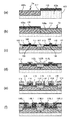
図2(a)は、反射型マスクブランクMの全体を示す平面図であり、図2(b)は、欠陥15を含む拡大図である。図2(c)と図2(d)は、A−A’線に沿った断面図であり、図2(c)は凸状欠陥の様子を示し、図2(d)は凹状欠陥の様子を示す。
FIG. 2A is a plan view showing the entirety of the reflective mask blank M, and FIG. 2B is an enlarged view including the
マスクブランクMは、マスク基板MS上に、波長(例えば、13.5nm)の露光光に対して反射率が十分に得られるように、Si(シリコン)とMo(モリブデン)を交互に積層した多層膜MLを形成したものである。 The mask blank M is a multilayer in which Si (silicon) and Mo (molybdenum) are alternately stacked on a mask substrate MS so that a sufficient reflectance can be obtained with respect to exposure light having a wavelength (for example, 13.5 nm). A film ML is formed.
多層膜MLを成膜する際、マスク基板MS上に、異物などの微細粒子が存在すると、多層膜MLはその影響を受けて、図2(c)に示すように、多層膜MLの表面が凸形状になって、凸状の位相欠陥16が発生する。逆に、マスク基板MSの表面に、微小な窪み、ピットが存在すると、図2(d)に示すように、多層膜MLの表面が凹形状になって、凹状の位相欠陥17が発生する。
When the multilayer film ML is formed, if fine particles such as foreign matter are present on the mask substrate MS, the multilayer film ML is affected by this, and the surface of the multilayer film ML is changed as shown in FIG. A
図3(a)は、凸状欠陥16を含むマスクブランクMの欠陥検出信号強度が最大となる検出状態を示す説明図である。図3(b)は、無欠陥のマスクブランクMを検出光学系の合焦位置に配置した状態を示す説明図である。図3(c)は、凹状欠陥17を含むマスクブランクMの欠陥検出信号強度が最大となる検出状態を示す説明図である。ここでは、理解容易のため、ビームスプリッタBSを省いて、結像光学系Lの結像面IPにアレイセンサを配置して光強度を検出する例について説明する。
FIG. 3A is an explanatory diagram showing a detection state in which the defect detection signal intensity of the mask blank M including the
凸状欠陥16は、僅か6nm程度の小さな高さを有する。凹状欠陥17は、僅か6nm程度の小さな深さを有する。いずれの場合も、検査光BMをマスクブランクMに対して垂直に照射した状態で、結像面IPでの光強度が最大となるようにマスクブランクMの高さを調整する合焦制御を行い、その高さを最適フォーカス位置とみなす。
The
図3(b)に示す無欠陥のマスクブランクMについて合焦制御を行ったフォーカス位置を基準として、図3(a)に示すような凸状欠陥16が存在する場合、凸状欠陥16は凸面ミラーのように作用して、フォーカス位置は距離df1だけ光路長が短くなる向きにシフトする。一方、図3(c)に示すような凹状欠陥17が存在する場合、凹状欠陥17は凹面ミラーのように作用して、フォーカス位置は距離df2だけ光路長が長くなる向きにシフトする。
When the
図4は、結像面IPでの信号強度とフォーカス位置の関係を示すグラフである。縦軸は暗視野検出像の信号強度を示し、横軸はフォーカス位置(フォーカスレベル)を示す。フォーカス位置の値が大きいほど、マスクブランクMの位置は結像光学系Lから離れることを意味する。なお、無欠陥のマスクブランクMのフォーカス位置は0である。ここで、直径W=140nm、高さH=6nmの凸状欠陥と、直径W=140nm、深さH=6nmの凹状欠陥が存在する場合を例示している。 FIG. 4 is a graph showing the relationship between the signal intensity on the imaging plane IP and the focus position. The vertical axis represents the signal intensity of the dark field detection image, and the horizontal axis represents the focus position (focus level). It means that the position of the mask blank M is farther from the imaging optical system L as the value of the focus position is larger. The focus position of the defect-free mask blank M is 0. Here, a case where a convex defect having a diameter W = 140 nm and a height H = 6 nm and a concave defect having a diameter W = 140 nm and a depth H = 6 nm are illustrated.
図4を参照すると、凸状欠陥が存在する場合、合焦制御によるフォーカス位置は結像光学系Lに近づく方向にシフトし、一方、凹状欠陥が存在する場合、合焦制御によるフォーカス位置は結像光学系Lから離れる方向にシフトすることが判る。 Referring to FIG. 4, when there is a convex defect, the focus position by focusing control is shifted toward the imaging optical system L. On the other hand, when there is a concave defect, the focusing position by focusing control is fixed. It can be seen that the shift is away from the image optical system L.
本実施形態では、図1に示したように、結像光学系Lからの出射光束14をビームスプリッタBSによって2つの光束14a,14bに分岐し、2個の2次元アレイセンサSa,Sbを用いて各シフト量を同時計測している。
In the present embodiment, as shown in FIG. 1, the
ここで、結像光学系Lの倍率をMAGとして、2次元アレイセンサSaの受光面と光束14aの結像面IPaとの間の距離d1=MAG2×df1とし、2次元アレイセンサSbの受光面と光束14bの結像面IPbとの間の距離d2=MAG2×df2と設定することが好ましい。
Here, the magnification of the imaging optical system L is MAG, and the distance between the light receiving surface of the two-dimensional array sensor Sa and the imaging surface IPa of the
なお、図1に示す構成において、ビームスプリッタBSは、必要に応じて、移動させて集光光路から取り外し可能であることが好ましい。すなわち、1個の2次元アレイセンサSaのみで検査信号を取り込むようにした暗視野検出装置の構成も実現可能である。この場合、センサSaの受光面を、結像光学系Lの結像面IPaとほぼ一致するように配置することが好ましく、これにより受光面に到達する検査光の光量は約3倍になる。 In the configuration shown in FIG. 1, it is preferable that the beam splitter BS can be moved and detached from the condensing optical path as necessary. That is, it is possible to realize a configuration of a dark field detection apparatus in which an inspection signal is captured by only one two-dimensional array sensor Sa. In this case, it is preferable to arrange the light receiving surface of the sensor Sa so as to substantially coincide with the image forming surface IPa of the image forming optical system L, so that the amount of the inspection light reaching the light receiving surface is about three times.
次に、図5と図6に示すフローチャートを用いて、本実施形態に係るマスクブランク検査方法を詳細に説明する。 Next, the mask blank inspection method according to the present embodiment will be described in detail using the flowcharts shown in FIGS.
まず図5のステップs1において、図1に示すように、多層膜MLが形成された反射型マスクブランクMをステージ2に載置して、ステージ駆動部5によって所望のXY位置に位置決めを終えた後、検査光BMを照射し、マスクブランクMの被検査領域を照明する。
First, in step s1 of FIG. 5, as shown in FIG. 1, the reflective mask blank M on which the multilayer film ML is formed is placed on the
次にステップs2において、結像光学系Lからの出射光束14をビームスプリッタBSによって2つの光束14a,14bに分岐し、2次元アレイセンサSa,Sbを用いて各欠陥検出信号を取得する。各検出信号は信号蓄積部6,7に取り込まれて、続いてノイズ除去処理が施され(ステップs3)、そして、検出信号の位置を定義する画素番号の初期化処理を行う(ステップs4)。
Next, in step s2, the emitted
次にステップs5において、画像処理部8は、欠陥の有無の判断処理を行う。次にステップs6において、欠陥有りと判断した場合、ステップs7に移行して、欠陥の有無、個数、サイズ、位置などの欠陥情報をデータ管理システムなどに記録する。
In step s5, the
次にステップs8において、すべての画素の処理が終了したかの判断を行い、処理すべき画素が残っている場合は、画素番号を更新して(ステップs9)、ステップs5に移行し、再び欠陥の有無の判断処理を繰り返す。 Next, in step s8, it is determined whether or not the processing of all the pixels has been completed. If there are remaining pixels to be processed, the pixel number is updated (step s9), the process proceeds to step s5, and the defect is again detected. Repeat the process of determining whether or not there is any.
図6は、ステップs5における欠陥の有無の判断処理の詳細を示すフローチャートである。マスクブランクMに欠陥が存在すると、欠陥位置に対応する2次元アレイセンサSa,Sbの何れかの画素での信号レベルが増大する。同一の箇所の検査信号が、ビームスプリッタBSを介して2個の2次元アレイセンサSa,Sbに取り込まれるため、両センサの検査信号レベルが予め設定した所定の閾値THを超えるか否かを判断することにより、欠陥の有無を判定できる。 FIG. 6 is a flowchart showing details of the process for determining whether there is a defect in step s5. If there is a defect in the mask blank M, the signal level at any pixel of the two-dimensional array sensor Sa, Sb corresponding to the defect position increases. Since the inspection signals at the same location are taken into the two two-dimensional array sensors Sa and Sb via the beam splitter BS, it is determined whether or not the inspection signal levels of both sensors exceed a predetermined threshold TH. By doing so, the presence or absence of a defect can be determined.
具体的には、まずステップs51において、第1の2次元アレイセンサSaの所定の画素の信号と予め設定した閾値THとを比較する。画素の信号レベルが閾値TH以下であれば、ステップs52において、第2の2次元アレイセンサSbの対応する画素の信号と当該閾値THとを比較する。比較の結果、いずれの画素の信号レベルも閾値TH以下であれば、欠陥無しと判断できる(ステップs56)。 Specifically, first, in step s51, a signal of a predetermined pixel of the first two-dimensional array sensor Sa is compared with a preset threshold value TH. If the signal level of the pixel is equal to or lower than the threshold value TH, in step s52, the corresponding pixel signal of the second two-dimensional array sensor Sb is compared with the threshold value TH. As a result of the comparison, if the signal level of any pixel is equal to or lower than the threshold value TH, it can be determined that there is no defect (step s56).
一方、いずれの画素の信号レベルも閾値THより大きい場合、ステップs53において、今度は、第1の2次元アレイセンサSaの所定の画素の信号と第2の2次元アレイセンサSbの所定の画素の信号とを比較する。前者が後者より大きければ、凸型欠陥ありと判断する(ステップs54)。一方、前者が後者以下であれば、凹型欠陥ありと判断する(ステップs55)。 On the other hand, if the signal level of any pixel is greater than the threshold value TH, in step s53, the signal of the predetermined pixel of the first two-dimensional array sensor Sa and the predetermined pixel of the second two-dimensional array sensor Sb are now detected. Compare the signal. If the former is larger than the latter, it is determined that there is a convex defect (step s54). On the other hand, if the former is less than or equal to the latter, it is determined that there is a concave defect (step s55).
なお、欠陥判定に使用する閾値THは、光学系に起因したノイズや2次元アレイセンサ等の電気系ノイズなどに由来する検出信号のバックグラウンドレベルの影響を予め把握しておいて、その影響を受けないように設定することが望ましい。 Note that the threshold TH used for defect determination is obtained by grasping in advance the influence of the background level of the detection signal derived from noise caused by the optical system and electrical system noise such as a two-dimensional array sensor. It is desirable to set so as not to receive.
また、2次元アレイセンサSa,Sbは、同じレベルの光を受光したときに同じレベルの出力が得られるよう較正することが望ましい。このとき、ビームスプリッタBSで分岐される光束14a,14bの強度が異なる場合は、光束14a,14bの強度比に応じて2次元アレイセンサSa,Sbの感度を較正して、同じレベルの出力が得られるように調整することが望ましい。
The two-dimensional array sensors Sa and Sb are preferably calibrated so that the same level of output can be obtained when the same level of light is received. At this time, when the
図7(a)は、基準マーク18が形成されたマスクブランクMの全体を示す平面図である。図7(b)は、基準マーク18の拡大図であり、図7(c)は、図7(b)のB−B’線に沿った断面図である。
FIG. 7A is a plan view showing the entire mask blank M on which the
マスクブランクMは、一般に、矩形状をなし、4つの角部のうちの隣接する2つの各部近傍に基準マーク18を予め設けている。これらの基準マーク18は、多層膜MLの上に吸収体パターンを形成するときの基準点として機能するものであり、マスクブランクMの検査の際、アライメントスコープ(不図示)で計測することによって、マスクブランクMの基準座標を正確に決定できる。
The mask blank M generally has a rectangular shape, and a
マスクブランクMを構成する超平滑基板の表面の一部には、微細幅の凹部19がFIB(Focused Ion Beam)等により予め形成されている。凹部19を覆うように多層膜MLを堆積することにより、凹部19に対応した位置に基準マーク18が形成される。ここでは、一対の凹部19が1つの基準マーク18を構成する場合を例示している。
On a part of the surface of the ultra-smooth substrate constituting the mask blank M, a
凹部19をEUV光で観察した場合、大きな位相変化を伴ったパターン部として認識できる。したがって、基準マーク18をマスクブランクM上の座標の基準として用い、検出される欠陥の位置は、基準マーク18を基準とした相対座標で定義できる。
When the
基準マーク18は、電子線、紫外光、可視光を照射した場合も、その反射光からパターン検出が可能である。これにより、例えば、電子線を用いて吸収体パターンを形成する際、基準マーク18および欠陥は電子線により検出することが可能である。
Even when the
基準マーク18は、1つのマスクブランクMにつき2箇所またはそれ以上に配置することが好ましい。基準マーク18を2箇所またはそれ以上配置することで、マスクブランクMの回転ずれを測定でき、その修正や補正が可能となる。ただし、基準マーク18の配置個数があまり多すぎても基準座標の設定が難しくなるので、本実施形態では基準マーク18が2つの角部近傍に1個ずつ、合計2箇所に配置している。
The reference marks 18 are preferably arranged at two or more locations for one mask blank M. By arranging two or more
特に限定されないが、基準マーク18の平面寸法は、例えば、200〜2000nm程度である。なお、基準マークの形成方法は、上記に限られること無く、例えば、平坦基板面上に多層膜MLを形成した後、多層膜ML上にFIBや短波長レーザ光を照射しても、基準マークとして活用できる。また、マスクブランクMのエッジ位置を光学的に検出する方法を採用しても同等の効果が得られる。
Although not particularly limited, the planar dimension of the
次に、反射型露光マスクの製造方法について説明する。上述のように検査が済んだ反射型マスクブランクMの上には、集積回路パターンに対応した吸収体パターンが形成される。従来は、修正が困難な欠陥が検出された場合、たとえ微小サイズの欠陥であってもそのマスクブランクは不良品として取り扱われ、処分される。 Next, a method for manufacturing a reflective exposure mask will be described. On the reflective mask blank M that has been inspected as described above, an absorber pattern corresponding to the integrated circuit pattern is formed. Conventionally, when a defect that is difficult to correct is detected, even if the defect is a minute size, the mask blank is handled as a defective product and disposed of.
本実施形態では、マスクブランクMに、凸型欠陥や凹型欠陥などの各種欠陥が存在している場合でも、吸収体パターンで欠陥を覆い隠すことによって、マスクブランクの不良品率を削減している。 In the present embodiment, even when various defects such as a convex defect and a concave defect exist in the mask blank M, the defect rate of the mask blank is reduced by covering the defects with the absorber pattern. .
まず、上述した検査方法により、マスクブランクMの欠陥の位置情報を事前に記憶しておく。このとき上述した基準マーク18を利用することにより、欠陥の位置座標を正確に把握することができる。
First, the position information of the defect of the mask blank M is stored in advance by the inspection method described above. At this time, the position coordinates of the defect can be accurately grasped by using the
続いて、記憶した欠陥位置情報に基づいて、吸収体パターンの形成位置を規定するための吸収体パターンマスクとマスクブランクとの相対位置を決定する。このとき、例えば、吸収体パターンが欠陥を覆い隠すように、吸収体パターンマスクの位置決めが可能である。そして、決定した相対位置に基づいて、マスクブランクの上に吸収体パターンを形成する。得られた反射型露光マスクは、吸収体パターンの下に欠陥が隠れているため、半導体基板の露光投影には全く支障がない。 Subsequently, based on the stored defect position information, a relative position between the absorber pattern mask and the mask blank for defining the formation position of the absorber pattern is determined. At this time, for example, the absorber pattern mask can be positioned so that the absorber pattern covers the defect. Then, an absorber pattern is formed on the mask blank based on the determined relative position. The obtained reflective exposure mask has no hindrance to the exposure projection of the semiconductor substrate because the defect is hidden under the absorber pattern.
以上のように、本実施形態のマスクブランクの検査装置および検査方法を用いることによって、マスクブランクの位相欠陥となる表面凹凸を容易に判断できるので、欠陥生成要因の分析が可能になり、無欠陥マスクブランク製造技術の開発を促進できる。 As described above, by using the mask blank inspection apparatus and inspection method of the present embodiment, the surface unevenness that becomes the phase defect of the mask blank can be easily determined, so that it becomes possible to analyze the cause of defect generation, and no defect Development of mask blank manufacturing technology can be promoted.
さらに、位相欠陥の位置が特定できるので、多層膜の上に半導体回路などのマスクパターンを定義する吸収体パターンと位相欠陥との位置関係を操作することにより、製造する反射型露光マスクの歩留まりを向上させることができる。その結果、低コストの反射型露光マスクを供給することができる。 Furthermore, since the position of the phase defect can be specified, the yield of the reflective exposure mask to be manufactured can be increased by manipulating the positional relationship between the absorber pattern defining the mask pattern such as a semiconductor circuit on the multilayer film and the phase defect. Can be improved. As a result, a low-cost reflective exposure mask can be supplied.
また、反射型露光マスクを用いた露光処理では、マスクとウエハとの相対平面位置に吸収体パターンのシフト量を加味させることにより、多層膜マスクのパターンをウエハ上に位置合わせ良く形成できる。このため、半導体集積回路の性能、信頼性および歩留まりを向上させることが可能となる。また、反射型露光マスクのコスト低減により、高い性能が要求される半導体集積回路のコスト低減を推進できる。 In the exposure process using the reflective exposure mask, the pattern of the multilayer mask can be formed on the wafer with good alignment by adding the shift amount of the absorber pattern to the relative plane position between the mask and the wafer. For this reason, the performance, reliability, and yield of the semiconductor integrated circuit can be improved. Further, the cost reduction of the reflective exposure mask can promote the cost reduction of the semiconductor integrated circuit that requires high performance.
実施の形態2.
本実施形態では、図1に示した検査装置において、ビームスプリッタBSの代わりに、回折格子で構成された光分岐素子を使用した例を説明する。
In the present embodiment, an example will be described in which an optical branching element constituted by a diffraction grating is used instead of the beam splitter BS in the inspection apparatus shown in FIG.
図8(a)は、透過型の回折格子GR1を使用した例を示す構成図である。図8(b)は、反射型の回折格子GR2を使用した例を示す構成図である。光分岐素子以外の構成は、図1のものと同様であるため、重複説明を省く。 FIG. 8A is a configuration diagram showing an example in which a transmissive diffraction grating GR1 is used. FIG. 8B is a configuration diagram illustrating an example in which a reflective diffraction grating GR2 is used. Since the configuration other than the optical branching element is the same as that of FIG. 1, redundant description is omitted.
図8(a)において、回折格子GR1は、ステンシル透過型回折格子で構成され、例えば、ピッチ140nmの線状開口群を有する。結像光学系Lからの出射光束14が、回折格子GR1を通過すると、格子ピッチおよび光波長で定まる回折角に従って、数次の回折光に分かれる。そのうち+1次回折光を光束14aとして利用し、−1次回折光を光束14bとして利用することができる。
In FIG. 8A, the diffraction grating GR1 is formed of a stencil transmission type diffraction grating, and has, for example, a linear aperture group with a pitch of 140 nm. When the
図8(b)では、回折格子GR2は、反射型回折格子として構成され、光束14の平均入射角は、例えば、80度に設定される。結像光学系Lからの出射光束14が回折格子GR2に入射すると、格子ピッチおよび光波長で定まる回折角に従って、数次の回折光に分かれる。そのうち+1次回折光を光束14aとして利用し、−1次回折光を光束14bとして利用することができる。
In FIG. 8B, the diffraction grating GR2 is configured as a reflective diffraction grating, and the average incident angle of the
いずれの場合も、2次元アレイセンサSaは、正のデフォーカス像を検知するように、光束14aの結像面IPaから光進行方向に沿って所定距離d1だけ変位した位置に配置される。一方、2次元アレイセンサSbは、負のデフォーカス像を検知するように、光束14bの結像面IPbから光進行方向とは反対方向に所定距離d2だけ変位した位置に配置される。こうした配置により、センサSa,Sb間の間隔を数cm程度に維持することができる。なお、2次元アレイセンサSa,Sb間に余裕がある場合は、上記の+1次回折光と−1次回折光に限られること無く、0次回折光を2次元アレイセンサSa,Sbのいずれかに取り込むことも可能である。
In any case, the two-dimensional array sensor Sa is disposed at a position displaced by a predetermined distance d1 from the imaging plane IPa of the
回折格子GR1,GR2で分岐される光束14a,14bの強度が異なる場合は、光束14a,14bの強度比に応じて2次元アレイセンサSa,Sbの感度を較正して、同じレベルの出力が得られるように調整することが望ましい。
When the intensity of the
本実施形態では、製作の困難な多層膜ビームスプリッタを使用することなく、堅固な回折格子を使用できるという利点がある。また、2個のセンサSa,Sbを接近配置できるため、図1の配置よりも光学系の重心バランスが良く、ステージ2の走査に伴う振動の影響を受けにくい、という利点もある。 In this embodiment, there is an advantage that a rigid diffraction grating can be used without using a multilayer film beam splitter which is difficult to manufacture. Further, since the two sensors Sa and Sb can be arranged close to each other, there is an advantage that the center of gravity balance of the optical system is better than the arrangement shown in FIG.
なお、位相欠陥の凹凸の形状を判別できること、検出した欠陥座標を検知でき、さらに必要であれば欠陥座標情報を吸収体パターンの作成時に反映できることは、実施の形態1の場合と同様であることはいうまでも無い。 As in the case of the first embodiment, it is possible to determine the shape of the irregularities of the phase defect, to detect the detected defect coordinates, and to reflect the defect coordinate information when creating the absorber pattern if necessary. Needless to say.
実施の形態3.
本実施形態では、上述の反射型露光マスクを用いた投影露光方法および半導体集積回路の製造方法について説明する。
In the present embodiment, a projection exposure method using the above-described reflective exposure mask and a method for manufacturing a semiconductor integrated circuit will be described.
図9は、反射型露光装置の一例を示す構成図である。マスクMは、上述したマスク製造方法によって製造されたものである。光源40から発する中心波長13.5nmのEUV光は、複数の多層膜反射鏡で構成された照明光学系41を介して、マスクMのパターン面を照明する。パターン面からの反射光は、複数の多層膜反射鏡で構成された縮小投影光学系42(例えば、倍率1/4)を通過して、ウエハ43上に結像される。ウエハ43は面内で移動可能なステージ44に搭載されており、ステージ44の移動とパターン露光の繰返しにより、ウエハ43の所望の領域にマスクMに対応したパターンが転写される。
FIG. 9 is a block diagram showing an example of a reflective exposure apparatus. The mask M is manufactured by the mask manufacturing method described above. The EUV light having a center wavelength of 13.5 nm emitted from the
図10(a)〜(f)は、半導体集積回路の製造方法の一例を説明する断面図である。ここでは、ツイン・ウエル方式のCMIS(Complimentary MIS)回路を有する半導体集積回路を製造する場合を例示するが、他の種々の方式の回路にも本発明は適用可能である。 10A to 10F are cross-sectional views illustrating an example of a method for manufacturing a semiconductor integrated circuit. Here, a case of manufacturing a semiconductor integrated circuit having a twin well type CMIS (Complimentary MIS) circuit is illustrated, but the present invention can be applied to other various types of circuits.
半導体ウエハ103を構成する基板103sは、例えば、略円板状のn−型Si(シリコン)単結晶からなる。基板103sの上部には、例えばnウエル106nおよびpウエル106pが形成されている(図10(b)参照)。nウエル106nには、例えば、n型不純物のP(リン)またはAs(ヒ素)が導入されている。また、pウエル106pには、例えば、p型不純物のB(ホウ素)が導入されている。nウエルおよびpウエルは以下のようにして形成する。
The
まず、半導体基板103s上にマスク合わせ用のウエハライメントマークを形成する(図示せず)。このウエハライメントマークは選択酸化工程を付加してウエル形成時に作成することもできる。
First, a wafer alignment mark for mask alignment is formed on the
続いて、図10(a)に示すように、基板103s上に酸化膜117を形成し、そして、酸化膜117の上に、インプラ(イオン・インプランテーションの略称)マスク用のレジストパターン118を通常の光リソグラフィを用いて形成する。その後、P(リン)またはAsをイオン注入して、n型ウエル106nを形成する。
Subsequently, as shown in FIG. 10A, an
次に、アッシング処理を行ってレジストパターン118を除去し、酸化膜117を除去した後、図10(b)に示すように、基板103sの上に酸化膜119を形成し、そして、酸化膜119の上に、インプラマスク用のレジストパターン120を通常の光リソグラフィを用いて形成する。その後、B(ホウ素)をイオン注入して、p型ウエル106pを形成する。
Next, ashing is performed to remove the resist
次に、アッシング処理を行ってレジストパターン120を除去し、酸化膜119を除去した後、図10(c)に示すように、基板103sの上側主面に、例えば、酸化シリコン膜からなる分離用のフィールド絶縁膜107を溝型アイソレーションの形状で形成する。
Next, after performing the ashing process to remove the resist
このアイソレーション形状は、例えば、最小寸法がウエハ上で36nmと小さく、寸法精度が3.5nmと厳しい値が要求される。そのため、このアイソレーション作製時のリソグラフィとして、EUVリソグラフィを用いることができる。 For this isolation shape, for example, the minimum dimension is as small as 36 nm on the wafer, and the dimensional accuracy is required to be as severe as 3.5 nm. Therefore, EUV lithography can be used as the lithography for producing this isolation.
このフィールド絶縁膜107によって囲まれた活性領域には、nMISトランジスタQnおよびpMISトランジスタQpが形成される。各トランジスタのゲート絶縁膜108は、例えば、酸化シリコン膜からなり、熱酸化法などで形成される。
In the active region surrounded by the
また、各トランジスタのゲート電極109は、例えば、最小寸法がウエハ上で32nmと小さく、寸法精度が3nmと厳しい値が要求される。そのため、例えば、CVD法等を用いて低抵抗ポリシリコンからなるゲート形成膜を堆積した後、EUVリソグラフィを用いてレジストを形成し、エッチング処理によりゲート電極109を形成する。この工程のリソグラフィは、一般にゲート層用リソグラフィと称され、極めて微細でかつ高い寸法精度なパターン転写が求められる。
Further, the
nMISトランジスタQnの半導体領域110は、ゲート電極109をマスクとして基板103sに、例えば、P(リン)またはAsをイオン注入法等によって導入することにより、ゲート電極109に対して自己整合的に形成される。また、pMISトランジスタQpの半導体領域111は、ゲート電極109をマスクとして基板103sに、例えば、B(ホウ素)をイオン注入法等によって導入することにより、ゲート電極109に対して自己整合的に形成される。
The
ここで、ゲート電極9は、低抵抗ポリシリコンの単体膜で形成されることに限定されるものではなく種々変更可能である。例えば、ゲート電極9は、低抵抗ポリシリコン膜上にタングステンシリサイドやコバルトシリサイド等のようなシリサイド層を設けた、いわゆるポリサイド構造としてもよい。あるいは、ゲート電極9は、低抵抗ポリシリコン膜上に、窒化チタンや窒化タングステン等のようなバリア導体膜を介在し、さらにタングステン等のような金属膜を設けた、いわゆるポリメタル構造としてもよい。 Here, the gate electrode 9 is not limited to being formed of a single film of low resistance polysilicon, and can be variously changed. For example, the gate electrode 9 may have a so-called polycide structure in which a silicide layer such as tungsten silicide or cobalt silicide is provided on a low resistance polysilicon film. Alternatively, the gate electrode 9 may have a so-called polymetal structure in which a barrier conductor film such as titanium nitride or tungsten nitride is interposed on a low resistance polysilicon film and a metal film such as tungsten is further provided.
次に、図10(d)に示すように、基板103s上に、例えば、CVD法等を用いて酸化シリコン膜からなる層間絶縁膜112を堆積した後、層間絶縁膜112の上面に配線用のポリシリコン膜をCVD法等によって堆積する。続いて、このポリシリコン膜上にリソグラフィを実施し、エッチングによりパターニングを行った後、パターニングされたポリシリコン膜の所定領域に不純物を導入することにより、ポリシリコン膜からなる配線113Lおよび抵抗113Rを形成する。
Next, as shown in FIG. 10D, after an
次に、図10(e)に示すように、基板103s上に、例えば、CVD法等を用いて酸化シリコン膜114を堆積する。そして、層間絶縁膜112および酸化シリコン膜114に対してEUVリソグラフィを用いてレジストを形成し、エッチング処理により、半導体領域110,111および配線113Lの一部が露出するような接続孔115を形成する。微細な孔は光回折の影響により解像しにくいので、この接続孔用リソグラフィには高い解像度を持ったEUVリソグラフィ技術を適用する。
Next, as shown in FIG. 10E, a
次に、図10(f)に示すように、基板103s上に、例えば、スパッタリング法やCVD法等を用いてTi(チタン)、TiNおよびW(タングステン)からなる金属膜を順次堆積した後、その金属膜の上に、EUVリソグラフィを用いてレジストを形成し、エッチング処理により、第1配線層116L1を形成する。第1配線層116L1は、微細な密集パターンと孤立パターンが含まれ、また近隣の配線を避けて配線を引き回したり、配線間を接続するため複雑なレイアウト形状となる。このため第1配線層のリソグラフィも高い解像度と寸法精度が要求される。
Next, as shown in FIG. 10F, after sequentially depositing a metal film made of Ti (titanium), TiN and W (tungsten) on the
これ以降も、第1配線層116L1と同様にして第2配線層(不図示)等を形成することにより、最終製品を製造することができる。 Thereafter, the final product can be manufactured by forming the second wiring layer (not shown) and the like in the same manner as the first wiring layer 116L1.
上述した一連の半導体装置の製造工程の中で、ゲート層用と接続孔および第1配線層用リソグラフィには十分高い解像性能が要求されるので、EUVリソグラフィを適用することが好ましい。 In the above-described series of semiconductor device manufacturing processes, sufficiently high resolution performance is required for the gate layer, the connection hole, and the first wiring layer lithography. Therefore, it is preferable to apply EUV lithography.
そしてゲート層用と第1配線層用のマスクには、実施の形態1〜2で説明した検査装置および方法を用いてマスクブランクを検査し、マスクブランク段階で無欠陥を確認したマスクを用いることが好ましい。 For the mask for the gate layer and the first wiring layer, the mask blank is inspected using the inspection apparatus and method described in the first and second embodiments, and a mask that has been checked for defects at the mask blank stage is used. Is preferred.
また接続孔(コンタクトホール)用マスクには、実施の形態1〜2で説明した検査装置および方法を用いてマスクブランクを検査し、マスクブランク段階で接続孔部付近に欠陥がないことを確認したマスクを用いることが好ましい。
接続孔の面積は小さく、またパターン密度も5%%程度であるため、接続孔付近に欠陥が発生する比率は少なく、この方法により使用できるマスクブランクの歩留まりは高くなる。従って、本実施形態により作製した半導体集積回路の歩留まりは、従来のマスクブランク欠陥検査を行って作製したものより高くなる。
Further, the mask for the connection hole (contact hole) was inspected by using the inspection apparatus and method described in the first and second embodiments, and it was confirmed that there was no defect near the connection hole at the mask blank stage. It is preferable to use a mask.
Since the area of the connection hole is small and the pattern density is about 5%, the ratio of defects near the connection hole is small, and the yield of the mask blank that can be used by this method is high. Therefore, the yield of the semiconductor integrated circuit manufactured according to this embodiment is higher than that manufactured by performing conventional mask blank defect inspection.
以上のように、実施の形態1〜2で説明した検査装置および方法を用いてマスクブランクを検査し、マスクブランク段階で無欠陥を確認したマスクを用いることにより、信頼性の高いマスクを用いたパターン転写を行なうことができる。このため、製造した半導体集積回路の性能、信頼性および歩留まりを向上させることが可能となり、その結果、半導体集積回路のコスト低減にも寄与できる。 As described above, a mask blank is inspected using the inspection apparatus and method described in the first and second embodiments, and a mask having no defects is used in the mask blank stage, thereby using a highly reliable mask. Pattern transfer can be performed. Therefore, it is possible to improve the performance, reliability, and yield of the manufactured semiconductor integrated circuit, and as a result, it is possible to contribute to cost reduction of the semiconductor integrated circuit.
以上、本発明を各実施形態を参照しつつ具体的に説明したが、本発明は上述した各実施形態に限定されるものではなく、本発明の範囲を逸脱しない範囲で種々変更可能であることはいうまでもない。 The present invention has been specifically described above with reference to each embodiment. However, the present invention is not limited to the above-described embodiment, and various modifications can be made without departing from the scope of the present invention. Needless to say.
本発明は、微細かつ高精度なパターンを含む半導体装置を高い生産効率で製造できる点で、産業上極めて有用である。 The present invention is extremely useful industrially in that a semiconductor device including a fine and highly accurate pattern can be manufactured with high production efficiency.
1 光源、 2 ステージ、 3 測長ミラー、 4 レーザ測長器、
5 ステージ駆動部、 6,7 信号蓄積部、 8 画像処理部、 9 主制御部、
10 ミラー、 12 レーザ光源、 13 センサ、 14,14a,14b 光束
18 基準マーク、 BS ビームスプリッタ、 DS 表示部、
IP,IPa,IPb 結像面、 L 結像光学系、 M マスクブランク、
MS マスク基板、 ML 多層膜、 Sa,Sb 2次元アレイセンサ、
103s 基板、 106n n型ウエル、 106p p型ウエル、
108 ゲート絶縁膜、 109 ゲート電極、 116L1 第1配線層。
1 light source, 2 stage, 3 measuring mirror, 4 laser measuring instrument,
5 stage drive unit, 6, 7 signal storage unit, 8 image processing unit, 9 main control unit,
10 mirror, 12 laser light source, 13 sensor, 14, 14a,
IP, IPa, IPb imaging surface, L imaging optical system, M mask blank,
MS mask substrate, ML multilayer film, Sa, Sb two-dimensional array sensor,
103s substrate, 106n n-type well, 106pp p-type well,
108 gate insulating film, 109 gate electrode, 116L1 first wiring layer.
Claims (4)
被検査領域から反射した光のうち鏡面反射光を除く散乱光を捕集し、捕集した光を第1光束および第2光束に分岐した後、第1光束の結像面から光進行方向に沿って所定距離だけ変位した位置に配置された第1画像センサ、および第2光束の結像面から光進行方向とは反対方向に所定距離だけ変位した位置に配置された第2画像センサをそれぞれ用いて、第1光束および第2光束が形成する各検査画像の強度分布を計測するステップと、
第1画像センサおよび第2画像センサからの各信号に基づいて、マスクブランクの欠陥の有無を判定するステップとを含み、
欠陥の有無を判定するステップは、
第1画像センサの信号と所定の第1閾値とを比較するステップと、
第2画像センサの信号と所定の第2閾値とを比較するステップと、
第1画像センサの信号と第2画像センサの信号とを比較するステップとを含み、
比較結果に基づいて、表面形状の凸型欠陥と凹型欠陥を識別することを特徴とするマスクブランク検査方法。 Irradiating inspection light toward the reflective mask blank to be inspected and illuminating the inspected area;
Scattered light other than specularly reflected light is collected from the light reflected from the region to be inspected. A first image sensor disposed at a position displaced along a predetermined distance along the second image sensor and a second image sensor disposed at a position displaced by a predetermined distance in the direction opposite to the light traveling direction from the imaging surface of the second light flux respectively. And measuring the intensity distribution of each inspection image formed by the first light beam and the second light beam,
Based on the signals from the first and second image sensors, see containing and determining the presence or absence of a defect of the mask blank,
The step of determining whether there is a defect is:
Comparing the signal of the first image sensor with a predetermined first threshold;
Comparing the signal of the second image sensor with a predetermined second threshold;
Comparing the signal of the first image sensor and the signal of the second image sensor,
A mask blank inspection method for identifying a convex defect and a concave defect of a surface shape based on a comparison result .
請求項1に記載されたマスクブランク検査方法を用いて、マスクブランクの欠陥を検査するステップと、
欠陥の位置情報を記憶するステップと、
記憶した欠陥位置情報に基づいて、吸収体パターンの形成位置を規定するための吸収体パターンマスクとマスクブランクとの相対位置を決定するステップと、
決定した相対位置に基づいて、マスクブランクの上に吸収体パターンを形成するステップとを含むことを特徴とする反射型露光マスクの製造方法。 A method of manufacturing a reflective exposure mask for forming an absorber pattern on a reflective mask blank,
Using the mask blank inspection method according to claim 1 for inspecting a mask blank for defects;
Storing defect position information;
Determining a relative position between the absorber pattern mask and the mask blank for defining the formation position of the absorber pattern based on the stored defect position information;
And a step of forming an absorber pattern on the mask blank based on the determined relative position.
Priority Applications (2)
| Application Number | Priority Date | Filing Date | Title |
|---|---|---|---|
| JP2007260796A JP5039495B2 (en) | 2007-10-04 | 2007-10-04 | Mask blank inspection method, reflective exposure mask manufacturing method, reflective exposure method, and semiconductor integrated circuit manufacturing method |
| US12/241,614 US7911600B2 (en) | 2007-10-04 | 2008-09-30 | Apparatus and a method for inspection of a mask blank, a method for manufacturing a reflective exposure mask, a method for reflective exposure, and a method for manufacturing semiconductor integrated circuits |
Applications Claiming Priority (1)
| Application Number | Priority Date | Filing Date | Title |
|---|---|---|---|
| JP2007260796A JP5039495B2 (en) | 2007-10-04 | 2007-10-04 | Mask blank inspection method, reflective exposure mask manufacturing method, reflective exposure method, and semiconductor integrated circuit manufacturing method |
Publications (3)
| Publication Number | Publication Date |
|---|---|
| JP2009092407A JP2009092407A (en) | 2009-04-30 |
| JP2009092407A5 JP2009092407A5 (en) | 2010-10-14 |
| JP5039495B2 true JP5039495B2 (en) | 2012-10-03 |
Family
ID=40522970
Family Applications (1)
| Application Number | Title | Priority Date | Filing Date |
|---|---|---|---|
| JP2007260796A Active JP5039495B2 (en) | 2007-10-04 | 2007-10-04 | Mask blank inspection method, reflective exposure mask manufacturing method, reflective exposure method, and semiconductor integrated circuit manufacturing method |
Country Status (2)
| Country | Link |
|---|---|
| US (1) | US7911600B2 (en) |
| JP (1) | JP5039495B2 (en) |
Families Citing this family (59)
| Publication number | Priority date | Publication date | Assignee | Title |
|---|---|---|---|---|
| KR101535230B1 (en) * | 2009-06-03 | 2015-07-09 | 삼성전자주식회사 | Apparatus and method for measuring an aerial image of EUV mask |
| EP2443440B1 (en) * | 2009-06-19 | 2019-11-27 | KLA-Tencor Corporation | Euv high throughput inspection system for defect detection on patterned euv masks, mask blanks, and wafers |
| JP6211270B2 (en) * | 2009-06-19 | 2017-10-11 | ケーエルエー−テンカー・コーポレーションKla−Tencor Corporation | Inspection system and method for defect detection of extreme ultraviolet mask blanks |
| NL2004949A (en) * | 2009-08-21 | 2011-02-22 | Asml Netherlands Bv | Inspection method and apparatus. |
| JP4715955B2 (en) * | 2009-10-23 | 2011-07-06 | レーザーテック株式会社 | Mask inspection method and mask inspection apparatus |
| JP5425593B2 (en) * | 2009-11-13 | 2014-02-26 | ルネサスエレクトロニクス株式会社 | EUV mask defect inspection method, EUV mask manufacturing method, EUV mask inspection apparatus, and semiconductor device manufacturing method |
| JP2012059984A (en) * | 2010-09-10 | 2012-03-22 | Nuflare Technology Inc | Mask inspection device and exposure mask manufacturing device |
| JP2012058206A (en) * | 2010-09-13 | 2012-03-22 | Toshiba Corp | Method and device for inspecting defect in mask |
| JP4822471B1 (en) * | 2010-11-30 | 2011-11-24 | レーザーテック株式会社 | EUV mask inspection apparatus and EUV mask inspection method |
| WO2012081587A1 (en) | 2010-12-14 | 2012-06-21 | 株式会社ニコン | Inspection method, inspection device, exposure management method, exposure system, and semiconductor device |
| JP5537443B2 (en) * | 2011-01-04 | 2014-07-02 | 株式会社東芝 | EUV mask blank quality determination method and EUV mask manufacturing method |
| WO2012114147A1 (en) * | 2011-02-23 | 2012-08-30 | Nano-Uv | Method for detecting defects in a microscopic scale on a surface of a sample, and device implementing this method |
| JP5566928B2 (en) * | 2011-03-04 | 2014-08-06 | 株式会社東芝 | Mask inspection method and apparatus |
| WO2012121159A1 (en) * | 2011-03-07 | 2012-09-13 | 旭硝子株式会社 | Multilayer substrate, manufacturing method for multilayer substrate, and quality control method for multilayer substrate |
| JP5814638B2 (en) * | 2011-06-08 | 2015-11-17 | 株式会社東芝 | Mask substrate defect inspection method and defect inspection apparatus, photomask manufacturing method and semiconductor device manufacturing method |
| WO2013013246A1 (en) | 2011-07-21 | 2013-01-24 | Brooks Automation, Inc. | Method and device for compensation for dimensional variations in low temperature sample group holders |
| JP5816499B2 (en) * | 2011-09-12 | 2015-11-18 | ルネサスエレクトロニクス株式会社 | Manufacturing method of EUV mask |
| US10197501B2 (en) | 2011-12-12 | 2019-02-05 | Kla-Tencor Corporation | Electron-bombarded charge-coupled device and inspection systems using EBCCD detectors |
| CN105549341A (en) | 2012-02-21 | 2016-05-04 | Asml荷兰有限公司 | Inspection apparatus and method |
| JP5126917B1 (en) * | 2012-03-14 | 2013-01-23 | レーザーテック株式会社 | Defect coordinate measuring apparatus, defect coordinate measuring method, mask manufacturing method, and reference mask |
| JP5944189B2 (en) | 2012-03-15 | 2016-07-05 | 株式会社東芝 | Mask substrate defect inspection method and defect inspection apparatus, photomask manufacturing method and semiconductor device manufacturing method |
| JP6009787B2 (en) * | 2012-03-16 | 2016-10-19 | 株式会社東芝 | Optimal imaging position detection method, optimal imaging position detection apparatus, photomask manufacturing method, and semiconductor device manufacturing method |
| US9496425B2 (en) | 2012-04-10 | 2016-11-15 | Kla-Tencor Corporation | Back-illuminated sensor with boron layer |
| US8953869B2 (en) | 2012-06-14 | 2015-02-10 | Kla-Tencor Corporation | Apparatus and methods for inspecting extreme ultra violet reticles |
| US9601299B2 (en) | 2012-08-03 | 2017-03-21 | Kla-Tencor Corporation | Photocathode including silicon substrate with boron layer |
| US9426400B2 (en) | 2012-12-10 | 2016-08-23 | Kla-Tencor Corporation | Method and apparatus for high speed acquisition of moving images using pulsed illumination |
| US10067419B2 (en) * | 2013-02-22 | 2018-09-04 | Hoya Corporation | Method for manufacturing reflective mask blank, and method for manufacturing reflective mask |
| US9632411B2 (en) | 2013-03-14 | 2017-04-25 | Applied Materials, Inc. | Vapor deposition deposited photoresist, and manufacturing and lithography systems therefor |
| US9417515B2 (en) | 2013-03-14 | 2016-08-16 | Applied Materials, Inc. | Ultra-smooth layer ultraviolet lithography mirrors and blanks, and manufacturing and lithography systems therefor |
| US9354508B2 (en) | 2013-03-12 | 2016-05-31 | Applied Materials, Inc. | Planarized extreme ultraviolet lithography blank, and manufacturing and lithography systems therefor |
| US20140272684A1 (en) | 2013-03-12 | 2014-09-18 | Applied Materials, Inc. | Extreme ultraviolet lithography mask blank manufacturing system and method of operation therefor |
| US9612521B2 (en) | 2013-03-12 | 2017-04-04 | Applied Materials, Inc. | Amorphous layer extreme ultraviolet lithography blank, and manufacturing and lithography systems therefor |
| US9448343B2 (en) * | 2013-03-15 | 2016-09-20 | Kla-Tencor Corporation | Segmented mirror apparatus for imaging and method of using the same |
| US9478402B2 (en) | 2013-04-01 | 2016-10-25 | Kla-Tencor Corporation | Photomultiplier tube, image sensor, and an inspection system using a PMT or image sensor |
| WO2014200648A2 (en) * | 2013-06-14 | 2014-12-18 | Kla-Tencor Corporation | System and method for determining the position of defects on objects, coordinate measuring unit and computer program for coordinate measuring unit |
| US9347890B2 (en) | 2013-12-19 | 2016-05-24 | Kla-Tencor Corporation | Low-noise sensor and an inspection system using a low-noise sensor |
| US9748294B2 (en) | 2014-01-10 | 2017-08-29 | Hamamatsu Photonics K.K. | Anti-reflection layer for back-illuminated sensor |
| US9410901B2 (en) | 2014-03-17 | 2016-08-09 | Kla-Tencor Corporation | Image sensor, an inspection system and a method of inspecting an article |
| DE102014211362B4 (en) | 2014-06-13 | 2018-05-09 | Carl Zeiss Smt Gmbh | Method for analyzing an optical element for the EUV wavelength range |
| JP6251647B2 (en) * | 2014-07-15 | 2017-12-20 | 株式会社ニューフレアテクノロジー | Mask inspection apparatus and mask inspection method |
| US9767986B2 (en) | 2014-08-29 | 2017-09-19 | Kla-Tencor Corporation | Scanning electron microscope and methods of inspecting and reviewing samples |
| KR102299921B1 (en) * | 2014-10-07 | 2021-09-09 | 삼성전자주식회사 | Optical apparatus |
| US9860466B2 (en) | 2015-05-14 | 2018-01-02 | Kla-Tencor Corporation | Sensor with electrically controllable aperture for inspection and metrology systems |
| US10748730B2 (en) | 2015-05-21 | 2020-08-18 | Kla-Tencor Corporation | Photocathode including field emitter array on a silicon substrate with boron layer |
| US10462391B2 (en) | 2015-08-14 | 2019-10-29 | Kla-Tencor Corporation | Dark-field inspection using a low-noise sensor |
| JP6394544B2 (en) * | 2015-09-04 | 2018-09-26 | 信越化学工業株式会社 | Photomask blank defect inspection method, sorting method, and manufacturing method |
| US10313622B2 (en) | 2016-04-06 | 2019-06-04 | Kla-Tencor Corporation | Dual-column-parallel CCD sensor and inspection systems using a sensor |
| US10778925B2 (en) | 2016-04-06 | 2020-09-15 | Kla-Tencor Corporation | Multiple column per channel CCD sensor architecture for inspection and metrology |
| US10359694B2 (en) * | 2016-08-31 | 2019-07-23 | Imec Vzw | Lithographic mask for EUV lithography |
| JP6891795B2 (en) * | 2017-01-26 | 2021-06-18 | 信越化学工業株式会社 | Defect inspection method, sorting method and manufacturing method of photomask blank |
| EP3355115B1 (en) * | 2017-01-26 | 2022-08-31 | Shin-Etsu Chemical Co., Ltd. | Methods and system for defect inspection, sorting and manufacturing photomask blanks |
| KR20190052516A (en) * | 2017-11-08 | 2019-05-16 | 삼성전자주식회사 | Surface inspection apparatus |
| US11114489B2 (en) | 2018-06-18 | 2021-09-07 | Kla-Tencor Corporation | Back-illuminated sensor and a method of manufacturing a sensor |
| KR102632562B1 (en) | 2018-08-22 | 2024-02-02 | 삼성전자주식회사 | Inspecting apparatus and method based on SI(Structured Illumination), and method for fabricating semiconductor device comprising the inspecting method |
| JP7154572B2 (en) * | 2018-09-12 | 2022-10-18 | Hoya株式会社 | MASK BLANK, TRANSFER MASK, AND METHOD FOR MANUFACTURING SEMICONDUCTOR DEVICE |
| US10943760B2 (en) | 2018-10-12 | 2021-03-09 | Kla Corporation | Electron gun and electron microscope |
| US11114491B2 (en) | 2018-12-12 | 2021-09-07 | Kla Corporation | Back-illuminated sensor and a method of manufacturing a sensor |
| JP7257853B2 (en) * | 2019-04-02 | 2023-04-14 | キヤノン株式会社 | POSITION DETECTION DEVICE, EXPOSURE DEVICE, AND PRODUCT MANUFACTURING METHOD |
| US11848350B2 (en) | 2020-04-08 | 2023-12-19 | Kla Corporation | Back-illuminated sensor and a method of manufacturing a sensor using a silicon on insulator wafer |
Family Cites Families (22)
| Publication number | Priority date | Publication date | Assignee | Title |
|---|---|---|---|---|
| JPH04328549A (en) * | 1991-04-26 | 1992-11-17 | Nikon Corp | Method and device for inspecting photomask |
| JP3336361B2 (en) | 1993-06-11 | 2002-10-21 | 株式会社ニコン | Inspection apparatus and inspection method for reflection type X-ray mask for reduction projection exposure |
| JP2002181723A (en) * | 1995-10-24 | 2002-06-26 | Nkk Corp | Surface inspection apparatus |
| JPH11354404A (en) | 1998-06-05 | 1999-12-24 | Hitachi Ltd | Method and apparatus for inspecting mask blank and reflecting mask |
| JP4576013B2 (en) * | 1999-12-21 | 2010-11-04 | オリンパス株式会社 | Optical encoder |
| JP3881125B2 (en) * | 1999-02-17 | 2007-02-14 | レーザーテック株式会社 | Level difference measuring apparatus and etching monitor apparatus and etching method using the level difference measuring apparatus |
| US6268093B1 (en) * | 1999-10-13 | 2001-07-31 | Applied Materials, Inc. | Method for reticle inspection using aerial imaging |
| JP3614741B2 (en) | 1999-12-17 | 2005-01-26 | 日立ハイテク電子エンジニアリング株式会社 | Defect detection optical system and the surface defect inspection apparatus |
| JP4230674B2 (en) * | 2001-03-01 | 2009-02-25 | 株式会社日立製作所 | Defect inspection apparatus and method |
| US6617603B2 (en) * | 2001-03-06 | 2003-09-09 | Hitachi Electronics Engineering Co., Ltd. | Surface defect tester |
| JP4084580B2 (en) | 2001-03-06 | 2008-04-30 | 株式会社日立ハイテクノロジーズ | Surface defect inspection equipment |
| JP2002286409A (en) * | 2001-03-26 | 2002-10-03 | Fuji Photo Optical Co Ltd | Interferometer |
| US6657714B2 (en) * | 2001-09-24 | 2003-12-02 | Applied Materials, Inc. | Defect detection with enhanced dynamic range |
| JP3728495B2 (en) | 2001-10-05 | 2005-12-21 | 独立行政法人産業技術総合研究所 | Multilayer mask defect inspection method and apparatus |
| US6914723B2 (en) * | 2001-11-09 | 2005-07-05 | Xradia, Inc. | Reflective lithography mask inspection tool based on achromatic Fresnel optics |
| JP2004193269A (en) * | 2002-12-10 | 2004-07-08 | Hitachi Ltd | Manufacturing method of mask, and manufacturing method of semiconductor integrated circuit device |
| JP2005156516A (en) * | 2003-11-05 | 2005-06-16 | Hitachi Ltd | Method of inspecting pattern defect, and apparatus of the same |
| JP4629372B2 (en) * | 2004-06-29 | 2011-02-09 | パナソニック株式会社 | Lens wavefront aberration inspection method and lens wavefront aberration inspection apparatus used therefor |
| US7769225B2 (en) * | 2005-08-02 | 2010-08-03 | Kla-Tencor Technologies Corp. | Methods and systems for detecting defects in a reticle design pattern |
| JP4723362B2 (en) * | 2005-11-29 | 2011-07-13 | 株式会社日立ハイテクノロジーズ | Optical inspection apparatus and method |
| JP2007219130A (en) * | 2006-02-16 | 2007-08-30 | Renesas Technology Corp | Defect inspection method and defect inspection device for mask blank, and method for manufacturing semiconductor device using them |
| US7782452B2 (en) * | 2007-08-31 | 2010-08-24 | Kla-Tencor Technologies Corp. | Systems and method for simultaneously inspecting a specimen with two distinct channels |
-
2007
- 2007-10-04 JP JP2007260796A patent/JP5039495B2/en active Active
-
2008
- 2008-09-30 US US12/241,614 patent/US7911600B2/en active Active
Also Published As
| Publication number | Publication date |
|---|---|
| US20090091752A1 (en) | 2009-04-09 |
| JP2009092407A (en) | 2009-04-30 |
| US7911600B2 (en) | 2011-03-22 |
Similar Documents
| Publication | Publication Date | Title |
|---|---|---|
| JP5039495B2 (en) | Mask blank inspection method, reflective exposure mask manufacturing method, reflective exposure method, and semiconductor integrated circuit manufacturing method | |
| TWI551956B (en) | Inspection method and apparatus, lithographic apparatus, lithographic processing cell and device manufacturing method | |
| JP5992103B2 (en) | Position measuring apparatus, position measuring method, lithographic apparatus, and device manufacturing method | |
| JP4660533B2 (en) | Scatterometer and focus analysis method | |
| US7630068B2 (en) | Method and system of defect inspection for mask blank and method of manufacturing semiconductor device using the same | |
| KR102102302B1 (en) | Diffraction based overlay metrology tool and method | |
| JP4541374B2 (en) | Lithographic apparatus and device manufacturing method with use of reduced scribe lanes for substrate metrology | |
| US9829442B2 (en) | Defect inspecting method, sorting method and producing method for photomask blank | |
| US11385552B2 (en) | Method of measuring a structure, inspection apparatus, lithographic system and device manufacturing method | |
| JP4940218B2 (en) | Optical focus sensor, inspection apparatus, and lithography apparatus | |
| JP2010272553A (en) | Defect inspection device and defect inspection method for mask blank, and method of manufacturing semiconductor device | |
| JP2009251412A (en) | Device and method for inspecting mask blank, method of manufacturing reflection type exposure mask, and method of manufacturing semiconductor integrated circuit | |
| JP5425593B2 (en) | EUV mask defect inspection method, EUV mask manufacturing method, EUV mask inspection apparatus, and semiconductor device manufacturing method | |
| KR102160223B1 (en) | Device and method for focusing in inspection system | |
| JP4861363B2 (en) | Angle-resolved scatterometer and inspection method | |
| CN112262345B (en) | Measuring apparatus | |
| JPH11150063A (en) | Method for detecting positional deviation and manufacture of device using the same | |
| JP5751994B2 (en) | Mask blank defect inspection method | |
| JP2011108711A (en) | Method of inspecting defect of euv mask, method of manufacturing euv mask, and method of manufacturing semiconductor device | |
| WO2020126266A1 (en) | Method of measuring a parameter of a patterning process, metrology apparatus, target | |
| JP2006269669A (en) | Measuring device and measuring method, exposure apparatus and device manufacturing method | |
| JP2009071169A (en) | Method of manufacturing reflection type exposure mask, reflection type exposure method, and manufacturing method of semiconductor integrated circuit | |
| JP2013026424A (en) | Manufacturing method of semiconductor device | |
| JP2006012867A (en) | Method and device for measuring mark, method, device and system for exposure | |
| JP5846785B2 (en) | Projection exposure method, projection exposure apparatus, and mask pattern transfer method |
Legal Events
| Date | Code | Title | Description |
|---|---|---|---|
| A711 | Notification of change in applicant |
Free format text: JAPANESE INTERMEDIATE CODE: A712 Effective date: 20100512 |
|
| A521 | Request for written amendment filed |
Free format text: JAPANESE INTERMEDIATE CODE: A523 Effective date: 20100830 |
|
| A621 | Written request for application examination |
Free format text: JAPANESE INTERMEDIATE CODE: A621 Effective date: 20100830 |
|
| A977 | Report on retrieval |
Free format text: JAPANESE INTERMEDIATE CODE: A971007 Effective date: 20120313 |
|
| A131 | Notification of reasons for refusal |
Free format text: JAPANESE INTERMEDIATE CODE: A131 Effective date: 20120327 |
|
| A521 | Request for written amendment filed |
Free format text: JAPANESE INTERMEDIATE CODE: A523 Effective date: 20120518 |
|
| TRDD | Decision of grant or rejection written | ||
| A01 | Written decision to grant a patent or to grant a registration (utility model) |
Free format text: JAPANESE INTERMEDIATE CODE: A01 Effective date: 20120703 |
|
| A01 | Written decision to grant a patent or to grant a registration (utility model) |
Free format text: JAPANESE INTERMEDIATE CODE: A01 |
|
| A61 | First payment of annual fees (during grant procedure) |
Free format text: JAPANESE INTERMEDIATE CODE: A61 Effective date: 20120709 |
|
| FPAY | Renewal fee payment (event date is renewal date of database) |
Free format text: PAYMENT UNTIL: 20150713 Year of fee payment: 3 |
|
| R150 | Certificate of patent or registration of utility model |
Ref document number: 5039495 Country of ref document: JP Free format text: JAPANESE INTERMEDIATE CODE: R150 Free format text: JAPANESE INTERMEDIATE CODE: R150 |
|
| S531 | Written request for registration of change of domicile |
Free format text: JAPANESE INTERMEDIATE CODE: R313531 |
|
| R350 | Written notification of registration of transfer |
Free format text: JAPANESE INTERMEDIATE CODE: R350 |