JP6312379B2 - Lithographic apparatus, lithography method, lithography system, program, and article manufacturing method - Google Patents
Lithographic apparatus, lithography method, lithography system, program, and article manufacturing method Download PDFInfo
- Publication number
- JP6312379B2 JP6312379B2 JP2013150054A JP2013150054A JP6312379B2 JP 6312379 B2 JP6312379 B2 JP 6312379B2 JP 2013150054 A JP2013150054 A JP 2013150054A JP 2013150054 A JP2013150054 A JP 2013150054A JP 6312379 B2 JP6312379 B2 JP 6312379B2
- Authority
- JP
- Japan
- Prior art keywords
- substrate
- processing
- processing unit
- information
- pattern formation
- Prior art date
- Legal status (The legal status is an assumption and is not a legal conclusion. Google has not performed a legal analysis and makes no representation as to the accuracy of the status listed.)
- Active
Links
Images


Classifications
-
- G—PHYSICS
- G03—PHOTOGRAPHY; CINEMATOGRAPHY; ANALOGOUS TECHNIQUES USING WAVES OTHER THAN OPTICAL WAVES; ELECTROGRAPHY; HOLOGRAPHY
- G03F—PHOTOMECHANICAL PRODUCTION OF TEXTURED OR PATTERNED SURFACES, e.g. FOR PRINTING, FOR PROCESSING OF SEMICONDUCTOR DEVICES; MATERIALS THEREFOR; ORIGINALS THEREFOR; APPARATUS SPECIALLY ADAPTED THEREFOR
- G03F7/00—Photomechanical, e.g. photolithographic, production of textured or patterned surfaces, e.g. printing surfaces; Materials therefor, e.g. comprising photoresists; Apparatus specially adapted therefor
- G03F7/70—Microphotolithographic exposure; Apparatus therefor
- G03F7/70058—Mask illumination systems
- G03F7/70191—Optical correction elements, filters or phase plates for controlling intensity, wavelength, polarisation, phase or the like
-
- G—PHYSICS
- G03—PHOTOGRAPHY; CINEMATOGRAPHY; ANALOGOUS TECHNIQUES USING WAVES OTHER THAN OPTICAL WAVES; ELECTROGRAPHY; HOLOGRAPHY
- G03F—PHOTOMECHANICAL PRODUCTION OF TEXTURED OR PATTERNED SURFACES, e.g. FOR PRINTING, FOR PROCESSING OF SEMICONDUCTOR DEVICES; MATERIALS THEREFOR; ORIGINALS THEREFOR; APPARATUS SPECIALLY ADAPTED THEREFOR
- G03F7/00—Photomechanical, e.g. photolithographic, production of textured or patterned surfaces, e.g. printing surfaces; Materials therefor, e.g. comprising photoresists; Apparatus specially adapted therefor
- G03F7/0002—Lithographic processes using patterning methods other than those involving the exposure to radiation, e.g. by stamping
-
- G—PHYSICS
- G03—PHOTOGRAPHY; CINEMATOGRAPHY; ANALOGOUS TECHNIQUES USING WAVES OTHER THAN OPTICAL WAVES; ELECTROGRAPHY; HOLOGRAPHY
- G03F—PHOTOMECHANICAL PRODUCTION OF TEXTURED OR PATTERNED SURFACES, e.g. FOR PRINTING, FOR PROCESSING OF SEMICONDUCTOR DEVICES; MATERIALS THEREFOR; ORIGINALS THEREFOR; APPARATUS SPECIALLY ADAPTED THEREFOR
- G03F7/00—Photomechanical, e.g. photolithographic, production of textured or patterned surfaces, e.g. printing surfaces; Materials therefor, e.g. comprising photoresists; Apparatus specially adapted therefor
- G03F7/70—Microphotolithographic exposure; Apparatus therefor
- G03F7/70483—Information management; Active and passive control; Testing; Wafer monitoring, e.g. pattern monitoring
-
- H—ELECTRICITY
- H01—ELECTRIC ELEMENTS
- H01J—ELECTRIC DISCHARGE TUBES OR DISCHARGE LAMPS
- H01J37/00—Discharge tubes with provision for introducing objects or material to be exposed to the discharge, e.g. for the purpose of examination or processing thereof
- H01J37/30—Electron-beam or ion-beam tubes for localised treatment of objects
- H01J37/317—Electron-beam or ion-beam tubes for localised treatment of objects for changing properties of the objects or for applying thin layers thereon, e.g. for ion implantation
- H01J37/3174—Particle-beam lithography, e.g. electron beam lithography
Description
本発明は、リソグラフィ装置、リソグラフィ方法、リソグラフィシステム、プログラム、および物品の製造方法に関する。 The present invention relates to a lithographic apparatus, a lithographic method, a lithographic system, a program, and an article manufacturing method.
リソグラフィ装置は、半導体デバイスやMEMSなどの物品の製造工程に含まれるリソグラフィ工程において、被加工物(基板)の上に加工のためのパターンを形成する。リソグラフィ装置の一例として、基板上の未硬化樹脂を型(モールド)で成形し、樹脂のパターンを基板上に形成するインプリント装置がある。光硬化法を採用したインプリント装置は、まず、基板上のインプリント領域(ショット領域)にインプリント材(光硬化性樹脂)を塗布する。次に、樹脂(未硬化樹脂)を型により成形する。そして、光を照射して樹脂を硬化させたうえで離型することにより、樹脂のパターンを基板上に形成する。特許文献1は、ステップアンドフラッシュ式のインプリント装置を開示している。 A lithographic apparatus forms a pattern for processing on a workpiece (substrate) in a lithography process included in a manufacturing process of an article such as a semiconductor device or a MEMS. As an example of a lithography apparatus, there is an imprint apparatus that forms an uncured resin on a substrate with a mold and forms a resin pattern on the substrate. An imprint apparatus that employs a photocuring method first applies an imprint material (photocurable resin) to an imprint region (shot region) on a substrate. Next, a resin (uncured resin) is molded with a mold. Then, the resin pattern is formed on the substrate by irradiating light to cure the resin and then releasing the mold. Patent Document 1 discloses a step-and-flash type imprint apparatus.
また、特許文献2は、生産性の向上のために、複数のリソグラフィ装置(例えば、露光装置またはインプリント装置)と、該複数のリソグラフィ装置に対して基板または原版を搬送する搬送ユニットとを含むクラスタ型のリソグラフィシステムを開示している。
Further,
従来のリソグラフィ工程では、露光装置の他に、基板上にレジスト(感光剤)を塗布する前処理と、露光済みの基板を現像する後処理とを行う塗布現像装置(コーター/デベロッパー)が用いられる。そして、塗布現像装置は、生産性や基板の清浄度の維持の観点から、露光装置と接続(いわゆるインライン接続)して用いられるのが一般的である。インプリント装置に関しても、パターンを形成する前に、洗浄や密着層の塗布などの基板に対する前処理を行う必要があるため、そのような前処理を行う前処理装置がインプリント装置に接続されて使用されうる。その場合、インプリント装置によるインプリント処理の直前に前処理装置による前処理が行われるのが望ましい。これは、インプリント処理では、基板上にゴミが付着していると、型や、型により形成される複数のインプリント領域のパターンの品位に影響を及ぼしうるためである。また、密着層が経時変化しうる場合もそうである。そのように前処理が行われるのが望ましい点は、他のリソグラフィ装置にもあてはまりうる。 In the conventional lithography process, in addition to the exposure apparatus, a coating / developing apparatus (coater / developer) that performs pre-processing for applying a resist (photosensitive agent) on a substrate and post-processing for developing an exposed substrate is used. . The coating and developing apparatus is generally used by being connected to an exposure apparatus (so-called inline connection) from the viewpoint of maintaining productivity and substrate cleanliness. Also regarding the imprint apparatus, it is necessary to perform pretreatment on the substrate such as cleaning and application of an adhesion layer before forming a pattern. Therefore, the pretreatment apparatus for performing such pretreatment is connected to the imprint apparatus. Can be used. In this case, it is desirable that preprocessing by the preprocessing device is performed immediately before imprint processing by the imprint device. This is because in the imprint process, if dust adheres to the substrate, it may affect the quality of the mold and the pattern of a plurality of imprint areas formed by the mold. This is also the case when the adhesion layer can change over time. The point that such pre-processing is desirable may also apply to other lithographic apparatus.
また、従来、1台の露光装置と1台の塗布現像装置とをインライン接続するのが一般的である。これに対して、リソグラフィ装置のスループット(単位時間当たりの基板処理枚数)より前処理装置のスループットが高い場合がある。この場合、1台の前処理装置に接続され、複数台のリソグラフィ装置(または複数のリソグラフィユニット)を含む所謂クラスタ型のリソグラフィ装置が必要となりうる。 Conventionally, one exposure apparatus and one coating and developing apparatus are generally connected in-line. On the other hand, the throughput of the preprocessing apparatus may be higher than the throughput of the lithography apparatus (the number of substrates processed per unit time). In this case, a so-called cluster type lithography apparatus that includes a plurality of lithography apparatuses (or a plurality of lithography units) connected to one pre-processing apparatus may be required.
そのようなクラスタ型のリソグラフィ装置の場合、同一ロット内の複数の基板を同一の装置(ユニット)で処理することが望ましい。そのように処理すると、同一ロット内の基板を同一の条件で処理できるため、その後の検査や処理などが容易となるためである。しかしながら、そのような処理を行うクラスタ型のリソグラフィ装置は、その生産性を考慮すると、複数のロットを並列に処理するのが好ましい。 In the case of such a cluster-type lithography apparatus, it is desirable to process a plurality of substrates in the same lot with the same apparatus (unit). This is because, if such processing is performed, the substrates in the same lot can be processed under the same conditions, so that subsequent inspection and processing are facilitated. However, a cluster-type lithography apparatus that performs such processing preferably processes a plurality of lots in parallel in view of productivity.
一方、前処理は、上記のとおり、リソグラフィ処理のできるだけ直前に行うのが有利である。そのため、クラスタ型のリソグラフィ装置での歩留まりおよび生産性を考慮すると、複数のロットにそれぞれ属する複数の基板を前処理装置が適時に処理して適時にリソグラフィ装置に提供するのが好ましい。 On the other hand, as described above, the pretreatment is advantageously performed immediately before the lithography process. Therefore, in consideration of the yield and productivity of the cluster-type lithography apparatus, it is preferable that the preprocessing apparatus processes the plurality of substrates respectively belonging to the plurality of lots in a timely manner and provides the lithographic apparatus in a timely manner.
本発明は、例えば、歩留まりおよび生産性の点で有利なリソグラフィ装置を提供することを目的とする。 An object of the present invention is to provide a lithographic apparatus that is advantageous in terms of yield and productivity, for example.
上記課題を解決するために、本発明は、前処理装置から供給された基板に対して、基板に対するレシピ情報に基づいて、パターン形成処理をそれぞれが行う複数の処理部を有するリソグラフィ装置であって、複数のロットのそれぞれに属する複数の基板に対して、並行したパターン形成処理を行うように、複数のロットのそれぞれに対応する複数のレシピ情報に基づいて複数の処理部を制御し、かつ前処理装置に対して基板を要求するタイミングを含む、並行したパターン形成処理のスケジュールに関する情報を前処理装置に送信する制御部を有することを特徴とする。 In order to solve the above-described problems, the present invention provides a lithography apparatus having a plurality of processing units each for performing pattern formation processing on a substrate supplied from a preprocessing device based on recipe information for the substrate. , for a plurality of substrates that belong to each of the plurality of lots, to perform parallel pattern forming process, and controls the plurality of processing units based on the plurality of recipe information corresponding to each of the plurality of lots, and before It has a control part which transmits the information regarding the schedule of the parallel pattern formation process including the timing which requests | requires a board | substrate with respect to a processing apparatus to a pre-processing apparatus.
本発明によれば、例えば、歩留まりおよび生産性の点で有利なリソグラフィ装置を提供することができる。 According to the present invention, for example, it is possible to provide a lithographic apparatus that is advantageous in terms of yield and productivity.
以下、本発明を実施するための形態について図面などを参照して説明する。 Hereinafter, embodiments for carrying out the present invention will be described with reference to the drawings.
まず、本発明の一実施形態に係るリソグラフィ装置について説明する。本実施形態に係るリソグラフィ装置は、後述する前処理装置から供給される基板に対してパターン形成処理をそれぞれ行う複数のリソグラフィ処理部を含む、いわゆるクラスタ型のリソグラフィ装置である。以下、本実施形態では、リソグラフィ処理部をインプリント処理部(インプリント装置)とした、クラスタ型インプリント装置を例に説明する。 First, a lithographic apparatus according to an embodiment of the present invention will be described. The lithographic apparatus according to the present embodiment is a so-called cluster type lithographic apparatus including a plurality of lithographic processing units that respectively perform pattern formation processing on a substrate supplied from a preprocessing apparatus to be described later. Hereinafter, in this embodiment, a cluster type imprint apparatus in which the lithography processing unit is an imprint processing unit (imprint apparatus) will be described as an example.
図1は、本実施形態に係るクラスタ型インプリント装置2と、このクラスタ型インプリント装置2を含むインプリントシステム1との構成を示す概略平面図である。インプリントシステム1は、クラスタ型インプリント装置2と、前処理装置3とを含む。クラスタ型インプリント装置2は、複数(本実施形態では一例として6つ)のインプリント処理部4(4A〜4F)と、基板搬送部5と、クラスタ制御部6とを含む。
FIG. 1 is a schematic plan view showing a configuration of a cluster
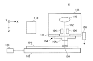
図2は、1つのインプリント処理部(以下、単に「処理部」と表記する)4の構成を示す概略図である。処理部4は、物品としての半導体デバイスなどの製造工程のうちのリソグラフィ工程を実施するもので、被処理基板であるウエハ101上(基板上)の未硬化樹脂109をモールド(型)104で成形し、ウエハ101上に樹脂109のパターンを形成する。なお、処理部4は、ここでは光硬化法を採用するものとする。また、以下の図においては、ウエハ101上の樹脂109に対して紫外線を照射する照明系107の光軸に平行にZ軸を取り、Z軸に垂直な平面内に互いに直交するX軸およびY軸を取っている。処理部4は、照明系107、モールド保持機構111およびアライメント計測系106とを含むインプリント構造体105と、ウエハステージ102と、塗布部108と、処理部内制御部110とを備える。
FIG. 2 is a schematic diagram showing a configuration of one imprint processing unit (hereinafter simply referred to as “processing unit”) 4. The
照明系107は、インプリント処理時に、光源から発せられた紫外線112をインプリントに適切な光に調整し、モールド104に照射する。光源は、水銀ランプなどのランプ類を採用可能であるが、モールド104を透過し、かつ樹脂(紫外線硬化樹脂)109が硬化する波長の光を発する光源であれば、特に限定するものではない。なお、本実施形態では、光硬化法を採用するので照明系107を設置しているが、例えば熱硬化法を採用する場合には、照明系107に換えて、熱硬化性樹脂を硬化させるための熱源部を設置することとなる。
The
モールド104は、外周形状が多角形(好適には、矩形または正方形)であり、ウエハ101に対する面には、例えば回路パターンなどの転写すべき凹凸パターンが3次元状に形成されたパターン部104aを含む。なお、パターンサイズは、製造対象となる物品により様々であるが、微細なものでは十数ナノメートルのパターンも含まれる。また、モールド104の材質は、紫外線112を透過させることが可能で、かつ熱膨張率の低いことが望ましく、例えば石英としうる。
The
モールド保持機構111は、不図示であるが、モールド104を保持するモールドチャックと、このモールドチャックを保持し、モールド104を移動させるモールド駆動機構とを有する。モールドチャックは、モールド104における紫外線112の照射面の外周領域を真空吸着力や静電力により引き付けることでモールド104を保持しうる。また、モールドチャックおよびモールド駆動機構は、照明系107から照射された紫外線112がモールド104を透過してウエハ101に向かうように、中心部(内側)に開口領域を有する。モールド駆動機構は、モールド104とウエハ101上の樹脂109との押し付けまたは引き離しを選択的に行うようにモールド104を各軸方向に移動させる。モールド駆動機構に採用可能な動力源としては、例えばリニアモーターまたはエアシリンダーがある。また、モールド104の高精度な位置決めに対応するために、粗動駆動系や微動駆動系などの複数の駆動系から構成されていてもよい。さらに、Z軸方向だけでなく、X軸方向やY軸方向、またはθ(Z軸周りの回転)方向の位置調整機能や、モールド104の傾きを補正するためのチルト機能などを有する構成もありうる。なお、インプリント処理時の押し付けおよび引き離し動作は、モールド104をZ軸方向に移動させることで実現してもよいが、ウエハステージ102をZ軸方向に移動させることで実現してもよく、または、その双方を相対的に移動させてもよい。
Although not shown, the
アライメント計測系106は、モールド104に予め形成されているアライメントマークと、ウエハ101に予め形成されているアライメントマークとを光学的に観察し、両者の相対位置関係を計測する。
The
ウエハ101は、例えば、単結晶シリコン基板やSOI(Silicon on Insulator)基板であり、この被処理面には、紫外線硬化樹脂であり、モールド104に形成されたパターン部104aにより成形される樹脂109が塗布される。
The
ウエハステージ102は、ウエハ101を保持し、モールド104とウエハ101上の樹脂109との押し付けに際して、モールド104と樹脂109との位置合わせを実施する。ウエハステージ102は、不図示であるが、ウエハ101を吸着力により保持するウエハチャックと、このウエハチャックを機械的手段により保持し、少なくともウエハ101の表面に沿う方向に移動可能とするステージ駆動機構とを有する。ステージ駆動機構に採用可能な動力源としては、例えばリニアモーターや平面モーターがあり、ステージ制御部103からの駆動指令に基づいて動作する。ステージ駆動機構も、X軸およびY軸の各方向に対して、粗動駆動系や微動駆動系などの複数の駆動系から構成されていてもよい。さらに、Z軸方向の位置調整のための駆動系や、ウエハ101のθ方向の位置調整機能、またはウエハ101の傾きを補正するためのチルト機能などを有する構成もありうる。
The
塗布部108は、モールド保持機構111の近傍に設置され、ウエハ101上に存在するパターン形成領域としてのショット上に、樹脂(未硬化樹脂)109を塗布する。ここで、樹脂109は、紫外線112を受光することにより硬化する性質を有する光硬化性樹脂(インプリント材)であり、デバイス製造工程などの各種条件により適宜選択される。また、塗布部108から塗布(吐出)される樹脂109の量も、ウエハ101上に形成される樹脂109の所望の厚さや、形成されるパターンの密度などにより適宜決定される。
The
処理部内制御部110は、処理部4の各構成要素の動作および調整などを制御する。処理部内制御部110は、不図示であるが、CPUまたはDSPなどの計算部と、レシピ情報などを記憶するメモリーやハードディスクなどの記憶部とを含む。ここで、レシピ情報は、ウエハ101、または同一の処理を行うウエハ群であるロットを処理する際の一連の処理パラメーターからなる情報(データ)である。処理パラメーターとしては、例えば、ショットのレイアウト、インプリント処理されるショットの順番、各ショットでのインプリント条件などである。また、インプリント条件としては、例えば、ウエハ101上に塗布した樹脂109にモールド104を押し付ける時間である充填時間や、紫外線112を照射して樹脂109を硬化させる時間である露光時間がある。インプリント条件として、さらには各ショット当たりに塗布する樹脂109の量である樹脂塗布量などもある。処理部内制御部110は、クラスタ制御部6からレシピを受信し、このレシピに基づいて、基板搬送部5により搬入されたウエハ101に対してインプリント処理を実施させる。
The processing unit
図1に戻り、基板搬送部5(図中の破線部分)は、各処理部4と前処理装置3との間でウエハ101を搬送(受け渡し)する。基板搬送部5としては、例えば、具体的には不図示であるが、ウエハ101を保持するハンドを含む搬送ロボットである。
Returning to FIG. 1, the substrate transfer unit 5 (broken line portion in the figure) transfers (transfers) the
クラスタ制御部(制御部)6は、クラスタ型インプリント装置2の各構成要素の動作および調整などを制御する。クラスタ制御部6は、例えば情報処理装置(コンピューター)で構成される。そして、本実施形態に係る処理(インプリント方法)は、プログラムとして上記情報処理装置に実行させうる。また、クラスタ制御部6と、各処理部4および基板搬送部5との間では、内部通信回線(通信回線)7により通信接続され、制御信号および各種情報(レシピ)が送受信される。
The cluster control unit (control unit) 6 controls the operation and adjustment of each component of the cluster
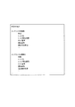
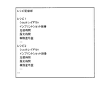
図3は、クラスタ制御部6の構成を示す概念図である。クラスタ制御部6は、主制御部301と、状態記録部302と、レシピ記録部303と、履歴記録部304とを含む。状態記録部302は、各処理部4の処理状態を記録する。図4は、状態記録部302に記録しているデータの一例を示す図である。状態記録部302は、処理部4ごとに、処理状態(処理中/処理待ち/停止中)、処理中のレシピを示すレシピ名、レシピの開始時間、または処理中のロットを示すロット番号などを記録する。状態記録部302は、さらには、処理中のウエハ101を示す基板番号や、処理を開始するウエハ101の開始時間を示す基板開始時間なども記録する。レシピ記録部303は、統括制御部10(後述)から受信した複数のレシピを記録する。図5は、レシピ記録部303に記録しているデータの一例を示す図である。レシピ記録部303に記録されうる内容は、処理部内制御部110の説明でも触れたとおりである。履歴記録部304は、過去に各処理部4で行ったインプリント処理の履歴情報(実績値)を記録する。さらに、図6は、履歴記録部304に記録しているデータの一例を示す図である。履歴記録部304は、処理部4ごとに、過去のインプリント処理のレシピ名、各ウエハ101の処理にかかった時間である基板処理時間などを記録する。そして、主制御部301は、状態記録部302、レシピ記録部303、履歴記録部304のデータ参照およびデータ設定を実行しながら、統括制御部10から受信したレシピに基づいてインプリント処理を行うよう各処理部4に指示を送信する。
FIG. 3 is a conceptual diagram showing the configuration of the
図1に再度戻り、前処理装置3は、クラスタ型インプリント装置2が指定したロットのウエハ101に対して、ウエハ101の洗浄や密着層の塗布などの前処理を行う洗浄装置または塗布装置などである。前処理装置3は、1ロットのウエハ101を格納する基板格納容器(FOUP)8を、その処理を担当する各処理部4に合わせた分、設置(収容)しうる。また、クラスタ制御部6と前処理装置3との間では、外部通信回線(通信回線)9により通信接続され、後述する基板要求スケジュールが送受信される。特に前処理装置3は、基板要求スケジュールに基づいて、クラスタ型インプリント装置2が前処理装置3に対して処理対象となるウエハ101を要求するタイミングに合わせて前処理が終了するように、複数のロット中のウエハ101を順不同で前処理を開始する。そして、前処理が完了したウエハ101は、一旦保持され、クラスタ型インプリント装置2からの基板要求に基づいて搬出される。
Returning to FIG. 1 again, the
さらに、統括制御部10は、従来、インプリント装置を用いて物品(例えば半導体デバイス)を製造する製造場所(例えば半導体製造工場)にて存在するもの同様、各種の製造装置との間でデータの送受信を行い、製造工程全体を統括制御するものである。本実施形態に係るクラスタ型インプリント装置2を含むインプリントシステム1も、他の製造装置と同様に、統括制御部10と、製造場所内のローカルエリアネットワークなどの通信網11で接続されている。
Further, the
次に、インプリントシステム1(クラスタ型インプリント装置2)におけるインプリント方法(リソグラフィ方法)について説明する。まず、クラスタ制御部6は、統括制御部10からの複数の要求(ロット番号とレシピとの組み合わせ)に対して、以下で説明する処理を各要求ごとに並行処理する。
Next, an imprint method (lithography method) in the imprint system 1 (cluster type imprint apparatus 2) will be described. First, in response to a plurality of requests (combination of lot numbers and recipes) from the
図7は、クラスタ制御部6が統括制御部10からの一要求に対して行う処理(以下「クラスタ構成インプリント処理」という)を示すフローチャートである。まず、クラスタ制御部6は、統括制御部10から、次に処理するロット(処理ロット)のロット番号およびそのロットに適用するレシピ(処理レシピ)を受信する(ステップS101)。また、クラスタ制御部6は、受信した処理レシピをレシピ記録部303に記録する。次に、クラスタ制御部6は、ステップS101で受信した処理ロットの処理を行う処理部4(以下「選択処理部」という。)を選択する(ステップS102)。このとき、クラスタ制御部6は、具体的には、内部の状態記録部302を参照し、処理を行っていない処理部4から選択処理部(以下、一例として処理部4Aが選択されたものとする。)を選択する。ここで、すべての処理部4が処理中の場合には、クラスタ制御部6は、いずれかの処理部4でロットの処理が終了するまで待機する。その後、クラスタ制御部6は、状態記録部302の選択処理部4Aの項目(例えば「インプリント処理部1」)に、状態、レシピ名、レシピ開始時間、ロット番号を記録する。なお、クラスタ制御部6は、ステップS101において統括制御部10から具体的に処理を担当する処理部4が指定され、その情報についても受信した場合には、その指定された処理部4を選択処理部とする。次に、クラスタ制御部6は、ステップS102で選択した選択処理部4Aに処理レシピを送信する(ステップS103)。次に、クラスタ制御部6は、前処理装置3に、処理ロットのウエハ101を要求する(ステップS104)。次に、クラスタ制御部6は、基板搬送部5に、ここで処理対象となるウエハ(対象ウエハ)101を前処理装置3から選択処理部4Aに搬送させる(ステップS105)。このとき、クラスタ制御部6は、さらに状態記録部302の選択処理部4Aの項目に、基板番号および基板開始時間を記録する。次に、クラスタ制御部6は、選択処理部4Aに、対象ウエハ101に対するインプリント処理を実施させる(ステップS106)。次に、クラスタ制御部6は、ステップS106におけるインプリント処理の終了後、基板搬送部5に、選択処理部4Aから処理済みの対象ウエハ101を搬出させ、前処理装置3に搬送させる(ステップS107)。次に、クラスタ制御部6は、この対象ウエハ101に対してステップS105からS107までの工程を行った際の基板処理時間を、レシピ名とともに履歴記録部304の選択処理部の項目のデータとして記録する(ステップS108)。次に、クラスタ制御部6は、処理ロットに含まれるすべてのウエハ101に対するステップS104からS109までの工程が終了したかどうかを判断する(ステップS109)。ここで、クラスタ制御部6は、終了したと判断した場合には(YES)、以下のステップS110に移行し、終了していないと判断した場合には(NO)、処理ロット内の次のウエハ101に対してステップS104以降の工程を実行する。そして、クラスタ制御部6は、処理ロットのインプリント処理が終了したことを統括制御部10に通知する(ステップS110)。また、クラスタ制御部6は、ここで状態記録部302の選択処理部の項目の情報(状態)を更新する。
FIG. 7 is a flowchart showing processing (hereinafter referred to as “cluster configuration imprint processing”) performed by the
一方、クラスタ制御部6は、上記のクラスタ構成インプリント処理と並行して、基板要求スケジュールを前処理装置3に送信する処理(以下「基板要求スケジュール送信処理」という。)を実行する。ここで、「基板要求スケジュール」とは、クラスタ制御部6から前処理装置3に対してウエハ101を要求するタイミングを含む情報である。基板要求スケジュール送信処理は、例えば、いずれかの処理部4でウエハ101に対する処理を開始または終了したタイミング(図7のステップS105またはステップS108に対応)で実行しうる。または、基板要求スケジュール送信処理を一定の時間間隔で実行しても構わない。
On the other hand, in parallel with the above-described cluster configuration imprint process, the
図8は、基板要求スケジュール送信処理を示すフローチャートである。まず、クラスタ制御部6は、各処理部4のそれぞれの基板処理スケジュールを生成する(ステップS201)。具体的には、まず、クラスタ制御部6は、各処理部4で処理中のレシピをレシピ記録部303から参照し、各ウエハ101の処理時間を推定する。そして、クラスタ制御部6は、状態記録部302から参照した処理部4の状態と、上記推定した各ウエハ101の処理時間とに基づいて、以降のウエハ101を要求するスケジュールを生成することができる。次に、クラスタ制御部6は、すべての処理部4に対してステップS201の工程が終了したかどうかを判断する(ステップS202)。ここで、クラスタ制御部6は、終了したと判断した場合には(YES)、以下のステップS203に移行し、終了していないと判断した場合には(NO)、すべての処理部4について終了するまでステップS201を繰り返す。次に、クラスタ制御部6は、ステップS201で求めた各処理部4の基板要求タイミングを合わせて時間順に並べて、すべての処理部4についての基板要求スケジュールを生成する(ステップS203)。
FIG. 8 is a flowchart showing the board request schedule transmission process. First, the
図9は、基板要求スケジュールの一例を示す図である。基板要求スケジュールは、各ウエハ101の要求ごとに、ウエハ101を要求する時刻、要求するウエハ101のロット番号、およびロット内の基板番号を含むデータである。なお、この例ではロット番号を前処理装置3に送信するものとしているが、例えば、前処理装置3がロットとそれを処理する処理部4との関係を記録および管理するものであれば、ロット番号に換えて処理部4を示す番号を送信するものとしてもよい。
FIG. 9 is a diagram illustrating an example of the board request schedule. The substrate request schedule is data including the time for requesting the
そして、クラスタ制御部6は、基板要求スケジュールを前処理装置3に送信する(ステップS204)。なお、この例では各処理部4で処理中のレシピから基板要求スケジュールを生成するものとしているが、例えば、履歴記録部304から過去の同一の処理部4の同一のレシピ実行時の処理時間を参照して基板要求スケジュールを生成してもよい。
Then, the
次に、各処理部において、アライメントマークが検出できないなどの例外処理が発生した場合または例外処理から復帰した場合の処理(以下「例外処理対応処理」という)について説明する。図10は、例外処理対応処理のフローチャートである。まず、クラスタ制御部6は、例外処理が発生した、または例外処理から復帰した処理部4から、その旨の信号を受信する(ステップS301)。次に、クラスタ制御部6は、状態記録部302に、当該処理部4が停止または復帰したことを記録する(ステップS302)。次に、クラスタ制御部6は、図8のステップS201からS202と同じ手順で、基板要求スケジュールを生成する(ステップS303)。ここで、例外処理が発生した場合については、当該処理部のウエハ101の要求は削除される。そして、クラスタ制御部6は、前処理装置3に、新規の基板要求スケジュールを再送信する(ステップS304)。
Next, a description will be given of a process (hereinafter referred to as “exception process corresponding process”) in the case where an exception process such as an alignment mark cannot be detected or a return from the exception process in each processing unit. FIG. 10 is a flowchart of exception handling handling processing. First, the
このように、クラスタ型インプリント装置2は、前処理装置3に対して、各処理部4にとって処理時間の観点から最も効率がよい基板要求スケジュールを送信するので、クラスタ型インプリント装置2全体の生産性を向上させることができる。さらに、この基板要求スケジュールにより、前記前処理装置3は、例えば、可能な限り各処理部4での処理の直前に密着層の塗布を実施することもできる。したがって、クラスタ型インプリント装置2は、歩留まりの低下を抑止することもできる。
As described above, the cluster
以上のように、本実施形態によれば、クラスタ構成とした場合に歩留まりおよび生産性を両立するリソグラフィ装置およびリソグラフィ方法、ならびにリソグラフィシステムを提供することができる。 As described above, according to the present embodiment, it is possible to provide a lithography apparatus, a lithography method, and a lithography system that can achieve both yield and productivity in a cluster configuration.
なお、上記説明では、クラスタ制御部6が、基板要求スケジュールを前処理装置3に送信するものとしているが、例えば、統括制御部10などの外部装置に送信し、この外部装置から前処理装置3の前処理開始タイミングを制御するものとしてもよい。また、上記説明では、各処理部4が、それぞれ1つのインプリント構造体105を備える構成としているが、それぞれ複数のインプリント構造体を備えるものとしてもよい。この場合、同一ロット内のウエハ101は、同一のインプリント構造体でインプリント処理されることが望ましい。
In the above description, the
さらに、上記説明では、リソグラフィ装置として、複数のインプリント処理部(インプリント装置)を含むクラスタ型インプリント装置を例示した。ただし、本発明は、これに限られるものではなく、例えば、電子線のような荷電粒子線で基板(基板上の感光剤)に描画処理を行う描画処理部(描画装置)を複数含むクラスタ型描画装置などにも適用可能である。 Furthermore, in the above description, a cluster type imprint apparatus including a plurality of imprint processing units (imprint apparatuses) is exemplified as the lithography apparatus. However, the present invention is not limited to this, for example, a cluster type including a plurality of drawing processing units (drawing apparatuses) that perform drawing processing on a substrate (photosensitive agent on the substrate) with a charged particle beam such as an electron beam. The present invention can also be applied to a drawing device.
(物品の製造方法)
一実施形態に係る物品の製造方法は、例えば、半導体デバイスなどのマイクロデバイスや微細構造を有する素子などの物品を製造するのに好適である。当該製造方法は、物体(例えば、感光剤を表面に有する基板)上に上記のリソグラフィ装置を用いてパターン(例えば潜像パターン)を形成する工程と、該工程でパターンを形成された物体を処理する工程(例えば、現像工程)とを含みうる。さらに、該製造方法は、他の周知の工程(酸化、成膜、蒸着、ドーピング、平坦化、エッチング、レジスト剥離、ダイシング、ボンディング、パッケージングなど)を含みうる。本実施形態の物品の製造方法は、従来の方法に比べて、物品の性能・品質・生産性・生産コストの少なくとも1つにおいて有利である。
(Product manufacturing method)
The method for manufacturing an article according to an embodiment is suitable for manufacturing an article such as a micro device such as a semiconductor device or an element having a fine structure. The manufacturing method includes a step of forming a pattern (for example, a latent image pattern) on an object (for example, a substrate having a photosensitive agent on the surface) by using the above-described lithography apparatus, and a processing of the object on which the pattern is formed in the step. (For example, development process). Further, the manufacturing method may include other well-known steps (oxidation, film formation, vapor deposition, doping, planarization, etching, resist stripping, dicing, bonding, packaging, and the like). The method for manufacturing an article according to the present embodiment is advantageous in at least one of the performance, quality, productivity, and production cost of the article as compared with the conventional method.
以上、本発明の好ましい実施形態について説明したが、本発明は、これらの実施形態に限定されず、その要旨の範囲内で種々の変形または変更が可能である。 As mentioned above, although preferable embodiment of this invention was described, this invention is not limited to these embodiment, A various deformation | transformation or change is possible within the range of the summary.
2 クラスタ型インプリント装置
3 前処理装置
4 処理部
6 クラスタ制御部
101 ウエハ
2 Cluster
Claims (32)
複数のロットのそれぞれに属する複数の前記基板に対して、並行したパターン形成処理を行うように、前記複数のロットのそれぞれに対応する複数のレシピ情報に基づいて前記複数の処理部を制御し、かつ前記前処理装置に対して前記基板を要求するタイミングを含む、前記並行したパターン形成処理のスケジュールに関する情報を前記前処理装置に送信する制御部を有することを特徴とするリソグラフィ装置。 A lithographic apparatus having a plurality of processing units each performing pattern formation processing based on recipe information for the substrate supplied from a pre-processing apparatus,
Control the plurality of processing units based on a plurality of recipe information corresponding to each of the plurality of lots so as to perform parallel pattern formation processing on the plurality of substrates belonging to each of the plurality of lots, A lithographic apparatus comprising: a control unit configured to transmit information regarding the schedule of the parallel pattern forming processes to the preprocessing apparatus, including timing for requesting the substrate from the preprocessing apparatus.
複数のロットのそれぞれに対応する複数のレシピ情報に基づいて、前記複数の処理部により前記複数のロットのそれぞれに属する複数の前記基板に対して、並行したパターン形成処理を行い、かつ前記前処理装置に対して前記基板を要求するタイミングを含む、前記並行したパターン形成処理のスケジュールに関する情報を生成し、
前記スケジュールに関する情報を前記前処理装置に送信する、
ことを特徴とするリソグラフィ方法。 A lithography method for performing pattern formation processing on a substrate supplied from a pretreatment apparatus in parallel in a plurality of processing units based on recipe information for the substrate,
Based on the plurality of recipe information corresponding to each of the plurality of lots, the plurality of processing units perform parallel pattern formation processing on the plurality of substrates belonging to each of the plurality of lots, and the preprocessing Generating information regarding the schedule of the parallel pattern formation process, including the timing of requesting the substrate to the apparatus;
Sending information about the schedule to the pre-processing device;
Lithographic method characterized by the above.
該リソグラフィ装置に基板を供給する前処理装置と、
を有することを特徴とするリソグラフィシステム。 A lithographic apparatus according to any one of claims 1 to 8,
A pretreatment apparatus for supplying a substrate to the lithographic apparatus;
A lithography system comprising:
前記工程で前記パターンを形成された基板を処理する工程と、
を含むことを特徴とする物品の製造方法。 Forming a pattern on a substrate using the lithographic apparatus according to any one of claims 1 to 8 or the lithographic method according to claim 9;
Processing the substrate on which the pattern is formed in the step;
A method for producing an article comprising:
複数のロットにそれぞれ対応する複数のレシピ情報に基づいて、前記複数の処理部により前記複数のロットのそれぞれに属する複数の基板に対して、並行したパターン形成処理を行い、かつ前記前処理装置に対して前記基板を要求するタイミングを含む、前記並行したパターン形成処理のスケジュールに関する情報を、生成し、
前記スケジュールに関する情報に基づいて、前記複数の基板に対する処理を前記前処理装置に行わせ、
前記前処理装置から供給された前記複数の基板に対する並行したパターン形成処理を前記リソグラフィ装置に行わせる、
ことを特徴とする方法。 A method of manufacturing an article by performing pattern formation processing on a substrate supplied from a pre-processing apparatus in parallel with a plurality of processing units included in the lithography apparatus based on recipe information for the substrate. ,
Based on a plurality of recipe information respectively corresponding to a plurality of lots, the plurality of processing units perform a parallel pattern formation process on a plurality of substrates belonging to each of the plurality of lots, and the preprocessing apparatus Generating information on a schedule of the parallel pattern forming processes, including timing for requesting the substrate to
Based on the information related to the schedule, let the pre-processing apparatus perform processing for the plurality of substrates,
Causing the lithography apparatus to perform parallel pattern formation processing on the plurality of substrates supplied from the pretreatment apparatus;
A method characterized by that.
インプリント処理によってパターン形成処理を基板に行う第1処理部と、
インプリント処理によってパターン形成処理を基板に行う第2処理部と、
第1ロットに属する第1基板のパターン形成処理を前記第1基板に対するレシピ情報に基づいて前記第1処理部が行い、かつ第2ロットに属する第2基板のパターン形成処理を前記第2基板に対するレシピ情報に基づいて前記第2処理部が行う並行したパターン形成処理を前記第1処理部および前記第2処理部に行わせ、前記第1処理部および前記第2処理部に前記基板を供給する前処理装置に対して、前記基板を要求するタイミングを含む、前記並行したパターン形成処理のスケジュールに関する情報を送信する制御部と、
を有するリソグラフィ装置。 A lithographic apparatus comprising:
A first processing unit that performs pattern formation processing on the substrate by imprint processing;
A second processing unit that performs pattern formation processing on the substrate by imprint processing;
The first processing unit performs pattern formation processing of the first substrate belonging to the first lot based on recipe information for the first substrate, and performs pattern formation processing of the second substrate belonging to the second lot to the second substrate. Based on the recipe information, the first processing unit and the second processing unit perform parallel pattern formation processing performed by the second processing unit, and supply the substrate to the first processing unit and the second processing unit. A control unit that transmits information regarding the schedule of the parallel pattern formation processing , including a timing of requesting the substrate, to the preprocessing apparatus;
A lithographic apparatus having:
インプリント処理によってパターン形成処理を基板に行う第1処理部と、
インプリント処理によってパターン形成処理を基板に行う第2処理部と、
第1ロットに属する第1基板に対するレシピ情報に基づいて前記第1処理部がパターン形成処理を前記第1基板に行い、かつ第2ロットに属する第2基板に対するレシピ情報に基づいて前記第2処理部がパターン形成処理を前記第2基板に行う並行したパターン形成処理のスケジュールに関する情報に基づいて、前記第1処理部に前記第1基板を搬送し、かつ前記第2処理部に前記第2基板を搬送する搬送部と、
前記第1処理部および前記第2処理部に前記並行したパターン形成処理を行わせ、前記搬送部に前記第1基板および前記第2基板を供給する前処理装置に対して、前記第1基板および前記第2基板を要求するタイミングを含む、前記並行したパターン形成処理のスケジュールに関する情報を送信する制御部と、
を有するリソグラフィ装置。 A lithographic apparatus comprising:
A first processing unit that performs pattern formation processing on the substrate by imprint processing;
A second processing unit that performs pattern formation processing on the substrate by imprint processing;
It performs the first processing unit is a pattern forming process based on the recipe information to the first substrate to the first substrate belonging to the first lot, and the second process based on recipe information to the second substrate belonging to the second lot The first substrate is transferred to the first processing unit and the second substrate is transferred to the second processing unit based on information on a schedule of parallel pattern forming processing in which the unit performs the pattern forming processing on the second substrate. A transport section for transporting
The pretreatment apparatus that causes the first processing unit and the second processing unit to perform the parallel pattern formation processing and supplies the first substrate and the second substrate to the transfer unit, the first substrate and A control unit for transmitting information on a schedule of the parallel pattern forming processes , including a timing for requesting the second substrate;
A lithographic apparatus having:
パターン形成処理を基板に行う第1処理部と、
パターン形成処理を基板に行う第2処理部と、
第1ロットに属する第1基板のパターン形成処理を前記第1基板に対するレシピ情報に基づいて前記第1処理部が行い、かつ第2ロットに属する第2基板のパターン形成処理を前記第2基板に対するレシピ情報に基づいて前記第2処理部が行う並行したパターン形成処理を前記第1処理部および前記第2処理部に行わせ、前記第1処理部および前記第2処理部に前記第1基板および前記第2基板を供給する前処理装置に対して、前記第1基板および前記第2基板を要求するタイミングを含む、前記並行したパターン形成処理のスケジュールに関する情報を送信する制御部と、
を有するリソグラフィ装置。 A lithographic apparatus comprising:
A first processing unit for performing pattern formation processing on the substrate;
A second processing unit for performing pattern formation processing on the substrate;
The first processing unit performs pattern formation processing of the first substrate belonging to the first lot based on recipe information for the first substrate, and performs pattern formation processing of the second substrate belonging to the second lot to the second substrate. The first processing unit and the second processing unit perform parallel pattern formation processing performed by the second processing unit based on the recipe information, and the first processing unit and the second processing unit have the first substrate and A control unit that transmits information on a schedule of the parallel pattern formation processes , including a timing of requesting the first substrate and the second substrate, to a pretreatment apparatus that supplies the second substrate;
A lithographic apparatus having:
第1ロットに属する第1基板に対するレシピ情報に基づいて前記第1処理部がパターン形成処理を前記第1基板に行い、かつ第2ロットに属する第2基板に対するレシピ情報に基づいて前記第2処理部がパターン形成処理を前記第2基板に行う並行したパターン形成処理のスケジュールに関する情報に基づいて、前記第1処理部に前記第1基板を搬送し、かつ前記第2処理部に前記第2基板を搬送し、
前記パターン形成処理のスケジュールに関する情報および前記搬送に関する情報に基づいて、前記第1基板および前記第2基板に前処理を行い、
前記並行したパターン形成処理を行う、
ことを特徴とするリソグラフィ方法。 A lithography method for performing pattern formation processing on a substrate using a first processing unit and a second processing unit,
It performs the first processing unit is a pattern forming process based on the recipe information to the first substrate to the first substrate belonging to the first lot, and the second process based on recipe information to the second substrate belonging to the second lot The first substrate is transferred to the first processing unit and the second substrate is transferred to the second processing unit based on information on a schedule of parallel pattern forming processing in which the unit performs the pattern forming processing on the second substrate. Transport the
Based on the information on the pattern formation processing schedule and the information on the transfer, pre-process the first substrate and the second substrate,
Performing the parallel pattern formation process;
Lithographic method characterized by the above.
第1ロットに属する第1基板に対するレシピ情報に基づいて前記第1処理部がパターン形成処理を前記第1基板に行い、かつ第2ロットに属する第2基板に対するレシピ情報に基づいて前記第2処理部がパターン形成処理を前記第2基板に行う並行したパターン形成処理および、前記第1処理部および前記第2処理部へ前記第1基板および前記第2基板を供給するタイミングを含む、スケジュールに関する情報を生成し、
生成された前記スケジュールに関する情報に基づいて、前記第1基板および前記第2基板に前処理を行い、
生成された前記スケジュールに関する情報に基づいて、前記並行したパターン形成処理を行う、
ことを特徴とするリソグラフィ方法。 A lithography method for performing pattern formation processing on a substrate using a first processing unit and a second processing unit,
It performs the first processing unit is a pattern forming process based on the recipe information to the first substrate to the first substrate belonging to the first lot, and the second process based on recipe information to the second substrate belonging to the second lot Information relating to a schedule, including a parallel pattern formation process in which a unit performs a pattern formation process on the second substrate, and a timing of supplying the first substrate and the second substrate to the first processing unit and the second processing unit Produces
Based on the generated information on the schedule , pre-process the first substrate and the second substrate,
Based on the generated information on the schedule , the parallel pattern formation processing is performed.
Lithographic method characterized by the above.
前記リソグラフィ装置に基板を供給する前処理装置と、
を有することを特徴とするリソグラフィシステム。 A lithographic apparatus according to any one of claims 14 to 25;
A pretreatment apparatus for supplying a substrate to the lithographic apparatus;
A lithography system comprising:
前記工程で前記パターン形成処理を行われた基板を処理する工程と、
を含むことを特徴とする物品の製造方法。 A step of performing pattern formation processing on a substrate using the lithography apparatus according to any one of claims 14 to 25;
Processing the substrate subjected to the pattern formation process in the step;
A method for producing an article comprising:
第1ロットに属する第1基板に対するレシピ情報に基づいて前記第1処理部がパターン形成処理を前記第1基板に行い、かつ第2ロットに属する第2基板に対するレシピ情報に基づいて前記第2処理部がパターン形成処理を前記第2基板に行う並行したパターン形成処理のスケジュールに関する情報に基づいて、前記第1処理部に前記第1基板を搬送し、かつ前記第2処理部に前記第2基板を搬送し、
前記パターン形成処理のスケジュールに関する情報および前記搬送に関する情報に基づいて、前記第1基板および前記第2基板に前処理を行い、
前記並行したパターン形成処理を行う、
ことを特徴とする方法。 A method of manufacturing an article by performing pattern formation processing on a substrate using a first processing unit and a second processing unit,
It performs the first processing unit is a pattern forming process based on the recipe information to the first substrate to the first substrate belonging to the first lot, and the second process based on recipe information to the second substrate belonging to the second lot The first substrate is transferred to the first processing unit and the second substrate is transferred to the second processing unit based on information on a schedule of parallel pattern forming processing in which the unit performs the pattern forming processing on the second substrate. Transport the
Based on the information on the pattern formation processing schedule and the information on the transfer, pre-process the first substrate and the second substrate,
Performing the parallel pattern formation process;
A method characterized by that.
第1ロットに属する第1基板に対するレシピ情報に基づいて前記第1処理部がパターン形成処理を前記第1基板に行い、かつ第2ロットに属する第2基板に対するレシピ情報に基づいて前記第2処理部がパターン形成処理を前記第2基板に行う並行したパターン形成処理および、前記第1処理部および前記第2処理部へ前記第1基板および前記第2基板を供給するタイミングを含む、スケジュールに関する情報を生成し、
生成された前記スケジュールに関する情報に基づいて、前記第1基板および前記第2基板に前処理を行い、
生成された前記スケジュールに関する情報に基づいて、前記並行したパターン形成処理を行う、
ことを特徴とする方法。 A method of manufacturing an article by performing pattern formation processing on a substrate using a first processing unit and a second processing unit,
It performs the first processing unit is a pattern forming process based on the recipe information to the first substrate to the first substrate belonging to the first lot, and the second process based on recipe information to the second substrate belonging to the second lot Information relating to a schedule, including a parallel pattern formation process in which a unit performs a pattern formation process on the second substrate, and a timing of supplying the first substrate and the second substrate to the first processing unit and the second processing unit Produces
Based on the generated information on the schedule , pre-process the first substrate and the second substrate,
Based on the generated information on the schedule , the parallel pattern formation processing is performed.
A method characterized by that.
Priority Applications (4)
| Application Number | Priority Date | Filing Date | Title |
|---|---|---|---|
| JP2013150054A JP6312379B2 (en) | 2013-07-19 | 2013-07-19 | Lithographic apparatus, lithography method, lithography system, program, and article manufacturing method |
| KR1020140087391A KR101758429B1 (en) | 2013-07-19 | 2014-07-11 | Lithography apparatus, lithography method, lithography system, storage medium, and article manufacturing method |
| US14/334,794 US9423700B2 (en) | 2013-07-19 | 2014-07-18 | Lithography apparatus, lithography method, lithography system, storage medium, and article manufacturing method |
| US15/221,985 US9880475B2 (en) | 2013-07-19 | 2016-07-28 | Lithography apparatus, lithography method, lithography system, storage medium, and article manufacturing method |
Applications Claiming Priority (1)
| Application Number | Priority Date | Filing Date | Title |
|---|---|---|---|
| JP2013150054A JP6312379B2 (en) | 2013-07-19 | 2013-07-19 | Lithographic apparatus, lithography method, lithography system, program, and article manufacturing method |
Publications (3)
| Publication Number | Publication Date |
|---|---|
| JP2015023146A JP2015023146A (en) | 2015-02-02 |
| JP2015023146A5 JP2015023146A5 (en) | 2016-09-08 |
| JP6312379B2 true JP6312379B2 (en) | 2018-04-18 |
Family
ID=52343343
Family Applications (1)
| Application Number | Title | Priority Date | Filing Date |
|---|---|---|---|
| JP2013150054A Active JP6312379B2 (en) | 2013-07-19 | 2013-07-19 | Lithographic apparatus, lithography method, lithography system, program, and article manufacturing method |
Country Status (3)
| Country | Link |
|---|---|
| US (2) | US9423700B2 (en) |
| JP (1) | JP6312379B2 (en) |
| KR (1) | KR101758429B1 (en) |
Families Citing this family (14)
| Publication number | Priority date | Publication date | Assignee | Title |
|---|---|---|---|---|
| JP6297001B2 (en) * | 2014-03-19 | 2018-03-20 | キヤノン株式会社 | Lithographic apparatus, lithography method, lithography system, program, and article manufacturing method |
| JP6324246B2 (en) * | 2014-07-11 | 2018-05-16 | キヤノン株式会社 | Lithographic apparatus and article manufacturing method |
| JP6399839B2 (en) * | 2014-07-15 | 2018-10-03 | キヤノン株式会社 | Imprint apparatus and article manufacturing method |
| US9927725B2 (en) | 2015-02-16 | 2018-03-27 | Canon Kabushiki Kaisha | Lithography apparatus, lithography method, program, lithography system, and article manufacturing method |
| JP6198805B2 (en) * | 2015-02-16 | 2017-09-20 | キヤノン株式会社 | Lithographic apparatus, lithography method, program, lithography system, and article manufacturing method |
| JP6438332B2 (en) * | 2015-03-18 | 2018-12-12 | キヤノン株式会社 | Imprint system and article manufacturing method |
| JP2016207755A (en) * | 2015-04-17 | 2016-12-08 | 株式会社ニコン | Exposure system and exchange method |
| EP3285281A4 (en) * | 2015-04-17 | 2019-05-08 | Nikon Corporation | Exposure system |
| JP6562707B2 (en) * | 2015-05-13 | 2019-08-21 | キヤノン株式会社 | Imprint apparatus, imprint method, and article manufacturing method |
| JP6320457B2 (en) * | 2016-05-31 | 2018-05-09 | キヤノン株式会社 | Substrate processing apparatus, substrate processing method, program, and article manufacturing method |
| US10969680B2 (en) | 2016-11-30 | 2021-04-06 | Canon Kabushiki Kaisha | System and method for adjusting a position of a template |
| JP6860365B2 (en) * | 2017-01-31 | 2021-04-14 | キヤノン株式会社 | Substrate processing equipment, substrate processing system, substrate processing method, article manufacturing method, and program |
| JP6853704B2 (en) * | 2017-03-22 | 2021-03-31 | キヤノン株式会社 | Lithography equipment and manufacturing method of goods |
| JP7112220B2 (en) * | 2017-05-12 | 2022-08-03 | キヤノン株式会社 | Methods, apparatus, systems, and methods of manufacturing articles |
Family Cites Families (15)
| Publication number | Priority date | Publication date | Assignee | Title |
|---|---|---|---|---|
| JPH0756619A (en) * | 1993-08-10 | 1995-03-03 | Nissan Motor Co Ltd | Production controller |
| US6466838B1 (en) * | 1998-05-14 | 2002-10-15 | Canon Kabushiki Kaisha | Semiconductor exposure apparatus and device manufacturing method using the same |
| JP4365934B2 (en) * | 1999-05-10 | 2009-11-18 | キヤノン株式会社 | Exposure apparatus, semiconductor manufacturing apparatus, and device manufacturing method |
| JP2000353649A (en) | 1999-06-09 | 2000-12-19 | Tokyo Electron Ltd | Method and apparatus for processing substrate |
| JP4915033B2 (en) * | 2000-06-15 | 2012-04-11 | 株式会社ニコン | Exposure apparatus, substrate processing apparatus, lithography system, and device manufacturing method |
| US20050137734A1 (en) | 2003-12-23 | 2005-06-23 | Asml Netherlands B.V. | Method of operating a lithographic apparatus or lithographic processsing cell, lithographic apparatus and lithographic processing cell |
| JP2006005285A (en) * | 2004-06-21 | 2006-01-05 | Canon Inc | Exposing line |
| US7798764B2 (en) * | 2005-12-22 | 2010-09-21 | Applied Materials, Inc. | Substrate processing sequence in a cartesian robot cluster tool |
| US7699021B2 (en) * | 2004-12-22 | 2010-04-20 | Sokudo Co., Ltd. | Cluster tool substrate throughput optimization |
| JP4509926B2 (en) * | 2005-12-27 | 2010-07-21 | 大日本スクリーン製造株式会社 | Substrate processing equipment |
| JP4185941B2 (en) | 2006-04-04 | 2008-11-26 | キヤノン株式会社 | Nanoimprint method and nanoimprint apparatus |
| JP5283842B2 (en) * | 2006-12-18 | 2013-09-04 | キヤノン株式会社 | Processing equipment |
| JP2011210992A (en) | 2010-03-30 | 2011-10-20 | Canon Inc | Lithography system, method of controlling lithography system, and device manufacturing method and article manufacturing method using lithography system |
| JP5411201B2 (en) * | 2010-05-21 | 2014-02-12 | 東京エレクトロン株式会社 | IMPRINT SYSTEM, IMPRINT METHOD, PROGRAM, AND COMPUTER STORAGE MEDIUM |
| TWI576670B (en) | 2011-04-22 | 2017-04-01 | 瑪波微影Ip公司 | Network architecture for lithography machine cluster |
-
2013
- 2013-07-19 JP JP2013150054A patent/JP6312379B2/en active Active
-
2014
- 2014-07-11 KR KR1020140087391A patent/KR101758429B1/en active IP Right Grant
- 2014-07-18 US US14/334,794 patent/US9423700B2/en active Active
-
2016
- 2016-07-28 US US15/221,985 patent/US9880475B2/en active Active
Also Published As
| Publication number | Publication date |
|---|---|
| KR101758429B1 (en) | 2017-07-14 |
| US9880475B2 (en) | 2018-01-30 |
| US9423700B2 (en) | 2016-08-23 |
| JP2015023146A (en) | 2015-02-02 |
| KR20150010601A (en) | 2015-01-28 |
| US20150022793A1 (en) | 2015-01-22 |
| US20160334714A1 (en) | 2016-11-17 |
Similar Documents
| Publication | Publication Date | Title |
|---|---|---|
| JP6312379B2 (en) | Lithographic apparatus, lithography method, lithography system, program, and article manufacturing method | |
| JP6198805B2 (en) | Lithographic apparatus, lithography method, program, lithography system, and article manufacturing method | |
| JP5754965B2 (en) | Imprint apparatus and article manufacturing method | |
| JP6399839B2 (en) | Imprint apparatus and article manufacturing method | |
| JP5072247B2 (en) | Lithographic apparatus and method, and device manufacturing method | |
| JP6297001B2 (en) | Lithographic apparatus, lithography method, lithography system, program, and article manufacturing method | |
| JP2013125817A (en) | Imprint device, imprint method, and article manufacturing method using the device or the method | |
| JP2011210992A (en) | Lithography system, method of controlling lithography system, and device manufacturing method and article manufacturing method using lithography system | |
| JP7270417B2 (en) | IMPRINT APPARATUS CONTROL METHOD, IMPRINT APPARATUS, AND ARTICLE MANUFACTURING METHOD | |
| JP2015023149A (en) | Imprint device, imprint method, program, imprint system, and method of manufacturing article using them | |
| JP2019102495A (en) | Information processing apparatus, program, lithographic apparatus, lithographic system, and method of manufacturing article | |
| JP2018163954A (en) | Lithographic apparatus and article manufacturing method | |
| JP2019046937A (en) | Substrate processing apparatus, substrate processing system, substrate processing method, program, and article manufacturing method | |
| JP2017199760A (en) | Imprint method, manufacturing method of material, and program | |
| JP2015023151A (en) | Imprint device, imprint method, program, imprint system, and method of manufacturing article using them | |
| US9927725B2 (en) | Lithography apparatus, lithography method, program, lithography system, and article manufacturing method | |
| KR102296682B1 (en) | Lithography apparatus, and method of manufacturing article | |
| JP6864447B2 (en) | Lithography equipment and manufacturing method of goods | |
| JP5871627B2 (en) | Imprint system and imprint method | |
| KR102192911B1 (en) | Stage apparatus, lithography apparatus, plate and article manufacturing method | |
| JP2023056322A (en) | Substrate conveying method, substrate conveying device, and method for manufacturing article | |
| JP2023183679A (en) | Substrate processing system and substrate processing method | |
| KR20180123630A (en) | Conveying device, system, and method of manufacturing article | |
| KR20180124732A (en) | Imprint method, imprint apparatus, imprint system, and method of manufacturing article | |
| JP2021068846A (en) | Imprinting device, imprinting method, and article manufacturing method |
Legal Events
| Date | Code | Title | Description |
|---|---|---|---|
| A521 | Request for written amendment filed |
Free format text: JAPANESE INTERMEDIATE CODE: A523 Effective date: 20160719 |
|
| A621 | Written request for application examination |
Free format text: JAPANESE INTERMEDIATE CODE: A621 Effective date: 20160719 |
|
| A977 | Report on retrieval |
Free format text: JAPANESE INTERMEDIATE CODE: A971007 Effective date: 20170411 |
|
| A131 | Notification of reasons for refusal |
Free format text: JAPANESE INTERMEDIATE CODE: A131 Effective date: 20170425 |
|
| A521 | Request for written amendment filed |
Free format text: JAPANESE INTERMEDIATE CODE: A523 Effective date: 20170626 |
|
| A131 | Notification of reasons for refusal |
Free format text: JAPANESE INTERMEDIATE CODE: A131 Effective date: 20171128 |
|
| A521 | Request for written amendment filed |
Free format text: JAPANESE INTERMEDIATE CODE: A523 Effective date: 20180129 |
|
| TRDD | Decision of grant or rejection written | ||
| A01 | Written decision to grant a patent or to grant a registration (utility model) |
Free format text: JAPANESE INTERMEDIATE CODE: A01 Effective date: 20180220 |
|
| A61 | First payment of annual fees (during grant procedure) |
Free format text: JAPANESE INTERMEDIATE CODE: A61 Effective date: 20180320 |
|
| R151 | Written notification of patent or utility model registration |
Ref document number: 6312379 Country of ref document: JP Free format text: JAPANESE INTERMEDIATE CODE: R151 |