JP6308958B2 - Substrate processing apparatus, substrate processing method, program, and computer storage medium - Google Patents
Substrate processing apparatus, substrate processing method, program, and computer storage medium Download PDFInfo
- Publication number
- JP6308958B2 JP6308958B2 JP2015035309A JP2015035309A JP6308958B2 JP 6308958 B2 JP6308958 B2 JP 6308958B2 JP 2015035309 A JP2015035309 A JP 2015035309A JP 2015035309 A JP2015035309 A JP 2015035309A JP 6308958 B2 JP6308958 B2 JP 6308958B2
- Authority
- JP
- Japan
- Prior art keywords
- substrate
- wafer
- shot
- exposure
- peripheral
- Prior art date
- Legal status (The legal status is an assumption and is not a legal conclusion. Google has not performed a legal analysis and makes no representation as to the accuracy of the status listed.)
- Active
Links
- 239000000758 substrate Substances 0.000 title claims description 157
- 238000012545 processing Methods 0.000 title claims description 78
- 238000003672 processing method Methods 0.000 title claims description 10
- 230000002093 peripheral effect Effects 0.000 claims description 109
- 238000007689 inspection Methods 0.000 claims description 29
- 230000007246 mechanism Effects 0.000 claims description 27
- 238000003384 imaging method Methods 0.000 claims description 19
- 238000000034 method Methods 0.000 claims description 17
- 235000012431 wafers Nutrition 0.000 description 155
- 238000012546 transfer Methods 0.000 description 42
- 230000008569 process Effects 0.000 description 14
- 239000011248 coating agent Substances 0.000 description 13
- 238000000576 coating method Methods 0.000 description 13
- 238000010438 heat treatment Methods 0.000 description 11
- 238000001514 detection method Methods 0.000 description 8
- 238000011161 development Methods 0.000 description 8
- 230000018109 developmental process Effects 0.000 description 8
- 238000005286 illumination Methods 0.000 description 6
- 230000012447 hatching Effects 0.000 description 4
- 239000007788 liquid Substances 0.000 description 3
- PXFBZOLANLWPMH-UHFFFAOYSA-N 16-Epiaffinine Natural products C1C(C2=CC=CC=C2N2)=C2C(=O)CC2C(=CC)CN(C)C1C2CO PXFBZOLANLWPMH-UHFFFAOYSA-N 0.000 description 2
- 239000007888 film coating Substances 0.000 description 2
- 238000009501 film coating Methods 0.000 description 2
- QSHDDOUJBYECFT-UHFFFAOYSA-N mercury Chemical compound [Hg] QSHDDOUJBYECFT-UHFFFAOYSA-N 0.000 description 2
- 229910052753 mercury Inorganic materials 0.000 description 2
- 238000012986 modification Methods 0.000 description 2
- 230000004048 modification Effects 0.000 description 2
- 238000000206 photolithography Methods 0.000 description 2
- 239000004065 semiconductor Substances 0.000 description 2
- 238000004528 spin coating Methods 0.000 description 2
- 230000009466 transformation Effects 0.000 description 2
- 238000004364 calculation method Methods 0.000 description 1
- 238000001816 cooling Methods 0.000 description 1
- 238000010586 diagram Methods 0.000 description 1
- 238000009434 installation Methods 0.000 description 1
- 230000001678 irradiating effect Effects 0.000 description 1
- 238000004519 manufacturing process Methods 0.000 description 1
- 230000003287 optical effect Effects 0.000 description 1
- 230000009467 reduction Effects 0.000 description 1
- 238000012360 testing method Methods 0.000 description 1
Images


Classifications
-
- G—PHYSICS
- G03—PHOTOGRAPHY; CINEMATOGRAPHY; ANALOGOUS TECHNIQUES USING WAVES OTHER THAN OPTICAL WAVES; ELECTROGRAPHY; HOLOGRAPHY
- G03F—PHOTOMECHANICAL PRODUCTION OF TEXTURED OR PATTERNED SURFACES, e.g. FOR PRINTING, FOR PROCESSING OF SEMICONDUCTOR DEVICES; MATERIALS THEREFOR; ORIGINALS THEREFOR; APPARATUS SPECIALLY ADAPTED THEREFOR
- G03F7/00—Photomechanical, e.g. photolithographic, production of textured or patterned surfaces, e.g. printing surfaces; Materials therefor, e.g. comprising photoresists; Apparatus specially adapted therefor
- G03F7/20—Exposure; Apparatus therefor
- G03F7/2022—Multi-step exposure, e.g. hybrid; backside exposure; blanket exposure, e.g. for image reversal; edge exposure, e.g. for edge bead removal; corrective exposure
- G03F7/2026—Multi-step exposure, e.g. hybrid; backside exposure; blanket exposure, e.g. for image reversal; edge exposure, e.g. for edge bead removal; corrective exposure for the removal of unwanted material, e.g. image or background correction
- G03F7/2028—Multi-step exposure, e.g. hybrid; backside exposure; blanket exposure, e.g. for image reversal; edge exposure, e.g. for edge bead removal; corrective exposure for the removal of unwanted material, e.g. image or background correction of an edge bead on wafers
-
- G—PHYSICS
- G03—PHOTOGRAPHY; CINEMATOGRAPHY; ANALOGOUS TECHNIQUES USING WAVES OTHER THAN OPTICAL WAVES; ELECTROGRAPHY; HOLOGRAPHY
- G03F—PHOTOMECHANICAL PRODUCTION OF TEXTURED OR PATTERNED SURFACES, e.g. FOR PRINTING, FOR PROCESSING OF SEMICONDUCTOR DEVICES; MATERIALS THEREFOR; ORIGINALS THEREFOR; APPARATUS SPECIALLY ADAPTED THEREFOR
- G03F7/00—Photomechanical, e.g. photolithographic, production of textured or patterned surfaces, e.g. printing surfaces; Materials therefor, e.g. comprising photoresists; Apparatus specially adapted therefor
- G03F7/20—Exposure; Apparatus therefor
- G03F7/2022—Multi-step exposure, e.g. hybrid; backside exposure; blanket exposure, e.g. for image reversal; edge exposure, e.g. for edge bead removal; corrective exposure
Description
本発明は、基板の周縁部に対して周辺露光処理を行う周辺露光装置、周辺露光方法、プログラム及びコンピュータ記憶媒体に関する。 The present invention relates to a peripheral exposure apparatus, a peripheral exposure method, a program, and a computer storage medium that perform peripheral exposure processing on a peripheral portion of a substrate.
例えば半導体デバイスの製造におけるフォトリソグラフィ処理では、例えば基板としての半導体ウェハ(以下、「ウェハ」という。)上にレジスト液を塗布してレジスト膜を形成するレジスト塗布処理、レジスト膜の周縁部を選択的に露光する周辺露光処理、周縁部が露光されたレジスト膜に所定のパターンを露光する露光処理、露光されたレジスト膜を現像する現像処理などが順次行われ、ウェハ上に所定のレジストのパターンが形成される。これらの一連の処理は、ウェハを処理する各種処理装置やウェハを搬送する搬送機構などを搭載した基板処理システム及び露光装置により行われる。 For example, in photolithography processing in the manufacture of semiconductor devices, for example, resist coating processing for forming a resist film by applying a resist solution on a semiconductor wafer (hereinafter referred to as “wafer”) as a substrate, and selecting the peripheral portion of the resist film A peripheral exposure process that exposes the target, an exposure process that exposes a predetermined pattern on the resist film that has been exposed to the peripheral edge, a development process that develops the exposed resist film, etc. Is formed. These series of processes are performed by a substrate processing system and an exposure apparatus equipped with various processing apparatuses for processing a wafer, a transfer mechanism for transferring a wafer, and the like.
ところで、周辺露光においては、ウェハをスピンチャックに保持した状態でレジスト膜の周縁部に光を照射し、スピンチャックを鉛直軸周りに回転させることで、ウェハ周縁部が所定幅でリング状に露光される。しかしながら、露光装置では矩形状のパターンの露光が行われるため、ウェハの周縁部には、周辺露光とパターン露光のいずれも行われない領域が存在することとなる。そのため、露光装置では、この露光が行われない領域に対して、いわゆるダミーショットと呼ばれる露光処理が行われる。 By the way, in the peripheral exposure, the peripheral edge of the resist film is irradiated with light while the wafer is held on the spin chuck, and the peripheral edge of the wafer is exposed in a ring shape with a predetermined width by rotating the spin chuck around the vertical axis. Is done. However, since exposure of a rectangular pattern is performed in the exposure apparatus, an area where neither peripheral exposure nor pattern exposure is performed exists at the peripheral edge of the wafer. Therefore, in the exposure apparatus, an exposure process called a so-called dummy shot is performed on an area where this exposure is not performed.
しかしながら、実際の製品に用いられないダミーショットを露光装置で行うことは、露光装置のスループットの低下を意味する。そのため、特許文献1では、周辺露光装置においてダミーショットを行うことが提案されている。具体的には、周辺露光装置においてウェハのオリエンテーションフラットやノッチを検出してウェハの位置を認識すると共に、ウェハの位置調整を行う。そして、光源をX方向及びY方向に走査することで、ウェハWの周縁部に矩形状のダミーショットが施される。
However, performing dummy shots that are not used in actual products with the exposure apparatus means a reduction in throughput of the exposure apparatus. For this reason,
ところで、一般的に、パターンのショットの配列方向と、ノッチとウェハの中心を結んだ線またはオリエンテーションフラットとは、直交あるいは平行の関係にある。そのため、特許文献1では、オリエンテーションフラットと平行または直交する方向に沿って周辺露光処理を行っている。
By the way, in general, the arrangement direction of the pattern shots and the line or orientation flat connecting the notch and the center of the wafer are orthogonal or parallel to each other. For this reason, in
しかしながら、露光装置で露光されるパターンのショットは、必ずしもオリエンテーションフラットや、ノッチとウェハの中心を結んだ線と、平行、直交した状態で配列しているとは限らない。かかる場合、ダミーショットのために光源を走査させるための情報としては、周辺露光装置で検出したオリエンテーションフラットやノッチの位置のみでは不十分である。 However, pattern shots exposed by the exposure apparatus are not necessarily arranged in a state of being parallel or orthogonal to an orientation flat or a line connecting the notch and the center of the wafer. In such a case, as information for scanning the light source for the dummy shot, only the position of the orientation flat or notch detected by the peripheral exposure apparatus is insufficient.
本発明は、かかる点に鑑みてなされたものであり、周辺露光装置により適切にダミーショットを行うことを目的としている。 The present invention has been made in view of this point, and an object thereof is to appropriately perform a dummy shot by a peripheral exposure apparatus.
レジスト膜が塗布された基板の周縁部を露光する周辺露光装置を備えた基板処理装置であって、前記周辺露光装置の外部に配置され、前記レジスト膜の塗布処理が施される前の既にパターン露光が行われパターンが形成された基板の表面を撮像して、基板画像を取得する検査装置を備え、前記周辺露光装置は、前記レジスト膜が塗布された基板を保持する基板保持部と、前記基板保持部に保持された基板の周縁部を露光する露光部と、前記基板保持部を移動及び回転させる第1の移動機構と、前記露光部を移動させる第2の移動機構と、前記レジスト膜が塗布された前記基板の周縁部が露光されるように、前記第1の移動機構及び前記第2の移動機構を制御する制御部と、を有し、該制御部は、前記レジスト膜が塗布された前記基板が当該周辺露光装置に搬入される前に、前記検査装置で取得した基板画像から、基板上のパターンのショットの配列情報を取得し、当該取得した配列情報に基づいて、前記第1の移動機構及び前記第2の移動機構を制御する処理レシピを作成することを特徴としている。 A substrate processing apparatus including a peripheral exposure apparatus that exposes a peripheral portion of a substrate coated with a resist film, the pattern being already placed before the resist film coating process is performed outside the peripheral exposure apparatus An inspection device that captures an image of the surface of a substrate on which a pattern has been formed by exposure and obtains a substrate image , wherein the peripheral exposure device includes a substrate holding unit that holds the substrate coated with the resist film , An exposure unit that exposes a peripheral portion of the substrate held by the substrate holding unit; a first moving mechanism that moves and rotates the substrate holding unit; a second moving mechanism that moves the exposure unit; and the resist film to but so that the exposed peripheral edge portion of the front Stories substrate coated, have a, and a controller which controls the first moving mechanism and the second moving mechanism, said control unit, the resist film The coated substrate is Before being carried into the exposure apparatus, pattern information on the pattern on the substrate is acquired from the substrate image acquired by the inspection apparatus, and the first moving mechanism and the first pattern are acquired based on the acquired array information. It is characterized in that a processing recipe for controlling the two movement mechanisms is created .
本発明によれば、パターン露光が行われた基板の基板画像から、基板上のパターンのショットの配列情報を取得し、当該取得した配列情報に基づいて第1の移動機構及び第2の移動機構を制御する制御部を有しているので、仮に、露光装置で露光されるパターンのショットの配列が、オリエンテーションフラットや、ノッチとウェハの中心を結んだ線と、平行、直交した状態ない場合であっても、取得した配列情報に基づいて、周縁部に適切にダミーショットを行うことができる。 According to the present invention, the arrangement information of the pattern shot on the substrate is acquired from the substrate image of the substrate on which the pattern exposure has been performed, and the first moving mechanism and the second moving mechanism are obtained based on the acquired arrangement information. If the pattern of the pattern shot exposed by the exposure device is not parallel or orthogonal to the orientation flat or the line connecting the notch and the center of the wafer. Even if it exists, based on the acquired arrangement | sequence information, a dummy shot can be appropriately performed to a peripheral part.
前記制御部では、前記基板画像から基板の中心位置及び基板のノッチ位置を検出し、当該基板の中心位置と基板のノッチ位置を結ぶ直線と、前記基板上のパターンのショットの配列方向とのなす角度を求め、当該求められた角度に応じて前記基板を回転させるべく前記第1の移動機構を制御してもよい。 The control unit detects the center position of the substrate and the notch position of the substrate from the substrate image, and forms a straight line connecting the center position of the substrate and the notch position of the substrate and the arrangement direction of the shots of the pattern on the substrate. seeking angles may control the first moving mechanism to rotate the substrate in accordance with the sought angle.
前記制御部では、前記基板画像から1のショットの寸法を算出すると共に、算出した寸法の前記ショットにより基板の全面を覆った場合に当該基板の外周端部と前記ショットが重なるか否かを判定し、前記基板の外周端部と前記ショットが重なる領域に存在するショットの座標を算出し、当該算出された座標に基づいて、前記処理レシピを作成してもよい。 The control unit calculates the size of one shot from the substrate image, and determines whether the shot is overlapped with the outer peripheral edge of the substrate when the entire surface of the substrate is covered with the shot of the calculated size. Then, the coordinates of a shot existing in an area where the outer peripheral edge of the substrate and the shot overlap may be calculated, and the processing recipe may be created based on the calculated coordinates.
前記検査装置は、複数の前記周辺露光装置に対して共通で設けられていてもよい。 The inspection apparatus may be provided in common for the plurality of peripheral exposure apparatuses.
別の観点による本発明は、周辺露光装置を備えた基板処理装置を用いた基板処理方法であって、前記基板処理装置は、前記周辺露光装置の外部に配置され、基板の表面を撮像して基板画像を取得する検査装置を備え、前記周辺露光装置は、レジスト膜が塗布された基板を保持する基板保持部と、前記基板保持部に保持された基板の周縁部を露光する露光部と、前記基板保持部を移動及び回転させる第1の移動機構と、前記露光部を移動させる第2の移動機構と、を有し、前記基板処理方法は、レジスト膜の塗布処理が施される前の既にパターン露光が行われパターンが形成された基板の表面を、前記検査装置で撮像して、基板画像を取得し、前記レジスト膜が塗布された前記基板が当該周辺露光装置に搬入される前に、前記検査装置で取得した基板画像から、基板上のパターンのショットの配列情報を取得し、当該取得した配列情報に基づいて、前記レジスト膜が塗布された前記基板の周縁部が露光されるように前記第1の移動機構及び前記第2の移動機構を制御する処理レシピを作成することを特徴としている。 The present invention according to another aspect is a substrate processing method using the substrate processing apparatus having a peripheral exposure apparatus, the substrate processing apparatus is located outside of the peripheral exposure device, by imaging a surface of the substrate An inspection apparatus for acquiring a substrate image, wherein the peripheral exposure apparatus includes a substrate holding unit that holds a substrate coated with a resist film , and an exposure unit that exposes a peripheral portion of the substrate held by the substrate holding unit; A first moving mechanism for moving and rotating the substrate holding portion; and a second moving mechanism for moving the exposure portion. The substrate processing method is a method before a resist film coating process is performed. The surface of the substrate on which the pattern exposure has already been performed and the pattern is formed is imaged by the inspection apparatus to obtain a substrate image, and before the substrate coated with the resist film is carried into the peripheral exposure apparatus Acquired by the inspection device From the substrate image to obtain the sequence information of the shot pattern on the substrate, based on the acquired sequence information, said first movement mechanism as the peripheral portion of the substrate on which the resist film is coated is exposed And the process recipe which controls the said 2nd moving mechanism is created, It is characterized by the above-mentioned.
前記基板画像から基板の中心位置及び基板のノッチ位置を検出し、当該基板の中心位置と基板のノッチ位置を結ぶ直線と、前記基板上のパターンのショットの配列方向とのなす角度を求め、当該求められた角度に応じて前記基板保持部を回転させてもよい。 Detecting the center position and the notch position of the substrate of the substrate from the substrate image, obtains a straight line connecting the center position and the notch position of the substrate of the substrate, the angle of the arrangement direction of the shot pattern on the substrate, The substrate holder may be rotated according to the determined angle.
前記基板画像から1のショットの寸法を算出すると共に、算出した寸法の前記ショットにより基板の全面を覆った場合に当該基板の外周端部と前記ショットが重なるか否かを判定し、前記基板の外周端部と前記ショットが重なる領域に存在するショットの座標を算出し、当該算出された座標に基づいて、前記処理レシピを作成してもよい。 The size of one shot is calculated from the substrate image, and when the entire surface of the substrate is covered with the shot of the calculated size, it is determined whether or not the shot is overlapped with the outer peripheral edge of the substrate, It is also possible to calculate the coordinates of a shot that exists in an area where the outer edge and the shot overlap, and create the processing recipe based on the calculated coordinates .
また別な観点による本発明によれば、前記基板処理方法を、基板処理装置によって実行させるように、当該基板処理装置を制御する制御部のコンピュータ上で動作するプログラムが提供される。 According to the present invention according to another aspect, the substrate processing method, as is performed by the substrate processing apparatus, a program running on a computer of a control unit for controlling the substrate processing apparatus is provided.
さらに別な観点による本発明によれば、前記プログラムを格納した読み取り可能なコンピュータ記憶媒体が提供される。 According to another aspect of the present invention, a readable computer storage medium storing the program is provided.
本発明によれば、周辺露光装置により適切にダミーショットを行うことができる。 According to the present invention, dummy shots can be appropriately performed by the peripheral exposure apparatus.
以下、本発明の実施の形態について説明する。図1は、本実施の形態にかかる周辺露光装置を備えた基板処理システム1の構成の概略を示す説明図である。図2及び図3は、各々基板処理システム1の内部構成の概略を模式的に示す、正面図と背面図である。なお、本実施の形態における基板処理システム1は、ウェハWに対して塗布現像処理を行う塗布現像処理システムである。
Embodiments of the present invention will be described below. FIG. 1 is an explanatory diagram showing an outline of a configuration of a
基板処理システム1は、図1に示すように複数枚のウェハWを収容したカセットCが搬入出されるカセットステーション10と、ウェハWに所定の処理を施す複数の各種処理装置を備えた処理ステーション11と、処理ステーション11に隣接する露光装置12との間でウェハWの受け渡しを行うインターフェイスステーション13とを一体に接続した構成を有している。
As shown in FIG. 1, the
カセットステーション10には、カセット載置台20が設けられている。カセット載置台20には、基板処理システム1の外部に対してカセットCを搬入出する際に、カセットCを載置するカセット載置板21が複数設けられている。
The
カセットステーション10には、図1に示すようにX方向に延びる搬送路22上を移動自在なウェハ搬送装置23が設けられている。ウェハ搬送装置23は、上下方向及び鉛直軸周り(θ方向)にも移動自在であり、各カセット載置板21上のカセットCと、後述する処理ステーション11の第3のブロックG3の受け渡し装置との間でウェハWを搬送できる。
As shown in FIG. 1, the
処理ステーション11には、各種装置を備えた複数例えば4つのブロックG1、G2、G3、G4が設けられている。例えば処理ステーション11の正面側(図1のX方向負方向側)には、第1のブロックG1が設けられ、処理ステーション11の背面側(図1のX方向正方向側)には、第2のブロックG2が設けられている。また、処理ステーション11のカセットステーション10側(図1のY方向負方向側)には、第3のブロックG3が設けられ、処理ステーション11のインターフェイスステーション13側(図1のY方向正方向側)には、第4のブロックG4が設けられている。
The
例えば第1のブロックG1には、図2に示すように複数の液処理装置、例えばウェハWを現像処理する現像処理装置30、ウェハWのレジスト膜の下層に反射防止膜(以下「下部反射防止膜」という)を形成する下部反射防止膜形成装置31、ウェハWにレジスト液を塗布してレジスト膜を形成するレジスト塗布装置32、ウェハWのレジスト膜の上層に反射防止膜(以下「上部反射防止膜」という)を形成する上部反射防止膜形成装置33が下からこの順に配置されている。
For example, in the first block G1, as shown in FIG. 2, a plurality of liquid processing apparatuses, for example, a
例えば現像処理装置30、下部反射防止膜形成装置31、レジスト塗布装置32、上部反射防止膜形成装置33は、それぞれ水平方向に3つ並べて配置されている。なお、これら現像処理装置30、下部反射防止膜形成装置31、レジスト塗布装置32、上部反射防止膜形成装置33の数や配置は、任意に選択できる。
For example, three
これら現像処理装置30、下部反射防止膜形成装置31、レジスト塗布装置32、上部反射防止膜形成装置33では、例えばウェハW上に所定の塗布液を塗布するスピンコーティングが行われる。スピンコーティングでは、例えば塗布ノズルからウェハW上に塗布液を吐出すると共に、ウェハWを回転させて、塗布液をウェハWの表面に拡散させる。
In the
例えば第2のブロックG2には、図3に示すようにウェハWの加熱や冷却といった熱処理を行う熱処理装置40や、レジスト液とウェハWとの定着性を高めるためのアドヒージョン装置41、ウェハWの外周部を露光する周辺露光装置42が上下方向と水平方向に並べて設けられている。これら熱処理装置40、アドヒージョン装置41、周辺露光装置42の数や配置についても、任意に選択できる。なお、周辺露光装置42の構成については後述する。
For example, in the second block G2, as shown in FIG. 3, a
例えば第3のブロックG3には、検査装置50と、複数の受け渡し装置51、52、53、54、55、56が下から順に設けられている。また、第4のブロックG4には、複数の受け渡し装置60、61、62が下から順に設けられている。検査装置50の構成については後述する。
For example, in the third block G3, an
図1に示すように第1のブロックG1〜第4のブロックG4に囲まれた領域には、ウェハ搬送領域Dが形成されている。ウェハ搬送領域Dには、例えばY方向、X方向、θ方向及び上下方向に移動自在な搬送アームを有する、ウェハ搬送装置70が複数配置されている。ウェハ搬送装置70は、ウェハ搬送領域D内を移動し、周囲の第1のブロックG1、第2のブロックG2、第3のブロックG3及び第4のブロックG4内の所定の装置にウェハWを搬送できる。
As shown in FIG. 1, a wafer transfer region D is formed in a region surrounded by the first block G1 to the fourth block G4. In the wafer transfer region D, for example, a plurality of
また、ウェハ搬送領域Dには、第3のブロックG3と第4のブロックG4との間で直線的にウェハWを搬送するシャトル搬送装置80が設けられている。
Further, in the wafer transfer region D, a
シャトル搬送装置80は、例えば図3のY方向に直線的に移動自在になっている。シャトル搬送装置80は、ウェハWを支持した状態でY方向に移動し、第3のブロックG3の受け渡し装置52と第4のブロックG4の受け渡し装置62との間でウェハWを搬送できる。
The
図1に示すように第3のブロックG3のX方向正方向側の隣には、ウェハ搬送装置90が設けられている。ウェハ搬送装置90は、例えばX方向、θ方向及び上下方向に移動自在な搬送アームを有している。ウェハ搬送装置90は、ウェハWを支持した状態で上下に移動して、第3のブロックG3内の各受け渡し装置にウェハWを搬送できる。
As shown in FIG. 1, a
インターフェイスステーション13には、ウェハ搬送装置100と受け渡し装置101が設けられている。ウェハ搬送装置100は、例えばY方向、θ方向及び上下方向に移動自在な搬送アームを有している。ウェハ搬送装置100は、例えば搬送アームにウェハWを支持して、第4のブロックG4内の各受け渡し装置、受け渡し装置101及び露光装置12との間でウェハWを搬送できる。
The
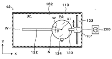
次に、周辺露光装置42の構成について説明する。周辺露光装置42は、図4及び図5に示すように筐体110を有している。筐体110の側面には、ウェハWを搬入出する、図示しない搬入出口が形成されている。筐体110の内部には、ウェハWを吸着保持する基板保持部としてのウェハチャック120が設けられている。ウェハチャック120は、水平な上面を有し、当該上面には、例えばウェハWを吸引する吸引口(図示せず)が設けられている。この吸引口からの吸引により、ウェハWをウェハチャック120上に吸着保持できる。
Next, the configuration of the
ウェハチャック120には、図5に示すように第1の移動機構としてのチャック駆動部121が取り付けられている。筐体110の底面には、筐体110内の一端側(図5中のX方向負方向側)から他端側(図5中のX方向正方向側)まで延伸するガイドレール122が設けられている。チャック駆動部121は、ガイドレール122上に設けられている。
As shown in FIG. 5, a
チャック駆動部121には、例えばモータ(図示せず)が内蔵されており、ウェハチャック120を回転させると共に、ガイドレール122に沿って、周辺露光装置42の外部との間でウェハWの受け渡しを行う受渡位置P1と、ウェハWの周縁部に対して周辺露光処理を行う周辺露光位置P2との間で移動自在に構成されている。
For example, a motor (not shown) is incorporated in the
筐体110の内部には、ウェハチャック120に保持されたウェハW上のレジスト膜の周縁部に光を照射して露光する露光部130が設けられている。露光部130には、当該露光部130に光を供給する光源としてランプハウス131が設けられている。ランプハウス131の内部には、超高圧水銀ランプ(図示せず)や超高圧水銀ランプからの光を集光する集光ミラー(図示せず)が設けられている。また、露光部130には、図示しない矩形状のスリットが設けられており、このスリットを通過した矩形状の光が露光部130から照射されるように構成されている。なお、矩形状の光を生成するスリットの開口は、後述するパターンのショットSHの寸法と同じか又は小さくなるように設定されている。これら露光部130とランプハウス131は、周辺露光位置P2よりX方向正方向側、すなわち筐体110のX方向正方向側の端部に配置されている。
An
ランプハウス131は、例えばその下面を、第2の移動機構としての露光駆動部132により支持されている。また、露光駆動部132の下面には、ガイドレール122と直交する方向(図4中のY方向)に沿って延伸するガイドレール133が設けられている。露光駆動部132には、例えばモータ(図示せず)が内蔵されており、ガイドレール133に沿って移動自在に構成されている。これにより、露光部130は、Y方向に沿ってウェハWの一端部から他端部上まで移動自在となっている。
転させてもよい。
For example, the lower surface of the
It may be turned.
筐体110の内部であって周辺露光位置P2には、ウェハチャック120に保持されたウェハWの周縁部の位置を検出する位置検出センサ134が設けられている。位置検出センサ134は例えばCCDカメラ(図示せず)を有し、周辺露光位置P2において、ウェハチャック120に保持されたウェハWの中心からの偏心量や、ウェハWのノッチ部Nの位置を検出する。また、位置検出センサ134によってノッチ部Nの位置を検出しながら、チャック駆動部121によってウェハチャック120を回転させて、ウェハWのノッチ部Nの位置を調整することができる。
A
これら、チャック駆動部121、露光駆動部132や、露光部130、位置検出センサ134といった、周辺露光装置42内の各機器は、後述する制御部200と接続されており、制御部200によりその動作が制御される。
Each device in the
次に、検査装置50の構成について説明する。
Next, the configuration of the
検査装置50は、図6に示すようにケーシング150を有している。ケーシング150内には、図7に示すようにウェハWを保持するウェハチャック151が設けられている。ケーシング150の底面には、ケーシング150内の一端側(図7中のX方向負方向側)から他端側(図7中のX方向正方向側)まで延伸するガイドレール152が設けられている。ガイドレール152上には、ウェハチャック151を回転させると共に、ガイドレール152に沿って移動自在な駆動部153が設けられている。
The
ケーシング150内の他端側(図5のX方向正方向側)の側面には、撮像部160が設けられている。撮像部160としては、例えば広角型のCCDカメラが用いられる。ケーシング150の上部中央付近には、ハーフミラー161が設けられている。ハーフミラー161は、撮像部160と対向する位置に、鏡面が鉛直下方を向いた状態から撮像部160の方向に向けて45度上方に傾斜した状態で設けられている。ハーフミラー161の上方には、照明装置162が設けられている。ハーフミラー161と照明装置162は、ケーシング150内部の上面に固定されている。照明装置162からの照明は、ハーフミラー161を通過して下方に向けて照らされる。したがって、照明装置162の下方にある物体によって反射した光は、ハーフミラー161でさらに反射して、撮像部160に取り込まれる。すなわち、撮像部160は、照明装置162による照射領域にある物体を撮像することができる。そして撮像したウェハWの画像(基板画像)は、後述する制御部200に入力される。
An
なお、本実施の形態では、検査装置50内に配置された撮像部160が、本発明の周辺露光装置42の撮像部として機能するものであり、当該撮像部160は、本実施の形態のごとく周辺露光装置42の外部に配置されていてもよい。
In the present embodiment, the
以上の基板処理システム1には、図1に示すように制御部200が設けられている。制御部200は、例えばコンピュータであり、プログラム格納部(図示せず)を有している。プログラム格納部には、基板処理システム1におけるウェハWの処理や搬送、ウェハWの周辺露光などを実行するプログラムが格納されている。なお、前記プログラムは、例えばコンピュータ読み取り可能なハードディスク(HD)、フレキシブルディスク(FD)、コンパクトディスク(CD)、マグネットオプティカルデスク(MO)、メモリーカードなどのコンピュータに読み取り可能な記憶媒体Hに記録されていたものであって、その記憶媒体Hから制御部200にインストールされたものであってもよい。
The
次に、以上のように構成された基板処理システム1を用いて行われるウェハWの処理方法について説明する。
Next, a processing method for the wafer W performed using the
先ず、複数のウェハWを収納したカセットCが、基板処理システム1のカセットステーション10に搬入される。このカセットC内の各ウェハWには既にパターン露光が行われ、例えば基板処理システム1外部の各種処理装置により、所定のパターンが形成されている。カセットC内のウェハWは、ウェハ搬送装置23により、先ず処理ステーション11の検査装置50に搬送される。
First, a cassette C storing a plurality of wafers W is carried into the
検査装置50では、ウェハWの表面が撮像部160により順次撮像され、ウェハW表面の画像(基板画像)が取得される。撮像部160で撮像された基板画像は、制御部200に入力される。
In the
制御部200では、基板画像に基づいて、ウェハW上に形成されたパターンの情報を取得する。具体的には、ウェハW上に図8に示すようにパターンのショットSHが配列している場合、制御部200では、ウェハWの基板画像IMから、ウェハWの中心位置CT、1のショットSHの寸法、ノッチ部Nの位置、及びショットSHの配列方向を取得する。ここで、ショットSHの配列方向は、ウェハWの中心位置CTとノッチ部Nの位置を結ぶ直線と、ショットSHの配列方向とのなす角θを算出することにより求められる。なお、図8では、例えば直径300mmのウェハWに、一辺15mmの正方形状にショットSHが形成されている場合の例を描図している。
The
次にウェハWは、第2のブロックG2の熱処理装置40に搬送され温度調節処理される。その後、ウェハWは、第1のブロックG1の下部反射防止膜形成装置31に搬送され、ウェハW上に下部反射防止膜が形成される。その後ウェハWは、第2のブロックG2の熱処理装置40に搬送され、加熱処理され、温度調節される。
Next, the wafer W is transferred to the
次にウェハWはアドヒージョン装置41に搬送され、アドヒージョン処理される。その後ウェハWは、第1のブロックG1のレジスト塗布装置32に搬送され、ウェハW上にレジスト膜が形成される。
Next, the wafer W is transferred to the
ウェハWにレジスト膜が形成されると、次にウェハWは、第1のブロックG1の上部反射防止膜形成装置33に搬送され、ウェハW上に上部反射防止膜が形成される。その後、ウェハWは第2のブロックG2の熱処理装置40に搬送され、加熱処理が行われる。その後、ウェハWは、ウェハ搬送装置70により、周辺露光装置42に搬送され、周辺露光処理される。
When the resist film is formed on the wafer W, the wafer W is then transferred to the upper antireflection
周辺露光装置42における周辺露光処置について詳述する。周辺露光装置42に搬送されたウェハWは、先ず、受渡位置P1においてウェハチャック120に受け渡される。この際、制御部200で基板画像IMから取得したウェハW中心位置CTと、ウェハチャック120の回転中心とが一致するように、ウェハ搬送装置70によりウェハWが受け渡される。その後、チャック駆動部121によって、ウェハチャック120を受渡位置P1から周辺露光位置P2側に移動させる。
The peripheral exposure treatment in the
ウェハチャック120に保持されたウェハWが周辺露光位置P2に移動すると、チャック駆動部121によってウェハWを回転させ、位置検出センサ134によりウェハWのノッチ部Nの位置を確認する。ノッチ部Nの位置が確認されると、次いで、制御部200により、ウェハチャック120に保持されたウェハWのノッチ部Nの位置が、例えば図9に示すように、ガイドレール122の延伸する方向から角度θずれるようにウェハチャック120が回転される。これにより、例えば図10に示すように、ショットSHの配列方向とガイドレール133の延伸する方向、即ち露光部130の移動する方向とが平行になり、露光部130をガイドレール133上で移動させることで、ショットSHの端部に沿って露光部130を移動させることができるようになる。
When the wafer W held on the
その後、ウェハWの周縁部に対して露光部130から光が照射され、ダミーショットが行われる。このダミーショットは、基板画像IMに基づいて制御部200で作成されたレシピに基づいて行われる。レシピの作成について具体的に説明する。
Thereafter, light is irradiated from the
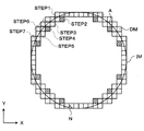
レシピの作成にあたり制御部200では、検査装置50で撮像された基板画像IMから求めた寸法のショットSHにより、例えば図11に示すように基板画像IMの全面を覆った場合に、基板画像IMの外周端部、即ちウェハWの外周端部とショットSHとが重なるか否かを判定する。そして、ショットSHの外周端部と重なる部分を図11に斜線で示すようにダミーショット領域DMと判定し、各ダミーショット領域DMの座標を算出する。なお、図11においては、例えば図12に斜線で示す、ウェハWの外周端部と重ならない領域Aについてもダミーショット領域DMとして表示しているが、不要部分のレジストを除去するという周辺露光処理の目的からは、図12に斜線で示す領域AについてはパターンのショットSHが形成されていないためダミーショットを行う必要がある。そのため、制御部200では、当該領域Aについてもダミーショット領域DMとして判定する。即ち、図12に斜線で示す領域Aは、例えば外周端部と重ならない部分及びショットSHのいずれにも属さない領域であり、このような領域Aもダミーショット領域DMとして判定される。
In creating the recipe, the
制御部200では、各ダミーショット領域DMの座標を算出した後に、各ダミーショット領域DMに対して周辺露光処理を行う順序を決定する。具体的には、例えば図12に破線で示すSTEP1〜STEP4のように、露光部130をガイドレール133に沿って、ウェハチャック120をガイドレール122に沿ってそれぞれ移動させることで露光可能なダミーショット領域DMに対して、先ず露光を行うようにレシピが作成される。この際、例えば図13に示すように、各STEP1〜STEP4においてダミーショットが行われるダミーショット領域DMの露光開始位置及び露光終了位置の座標が基板画像IMに基づいて算出される。なお、図13では、便宜上、各ダミーショット領域DMの右上の頂点の座標を記載している。
After calculating the coordinates of each dummy shot area DM, the
図12に示すSTEP5〜STEP7については、例えばウェハWを時計回りに90度回転させて周辺露光処理を行うことが好ましいため、露光順序はSTEP4の後に設定される。このSTEP5〜STEP7についても、同様にダミーショット領域DMの露光開始位置及び露光終了位置の座標が算出される。そして、STEP7以降も、順次ダミーショット領域DMの露光開始位置及び露光終了位置の座標が算出され、周辺露光処理のレシピが作成される。このレシピの作成は、検査装置50で基板画像IMが取得されたウェハWが周辺露光装置42に搬入される前に予め行われる。なお、位置検出センサ134での検出結果から、ウェハチャック120の回転中心とウェハWの中心位置CTとがずれて偏心した状態にある場合は、図13に示すX座標、Y座標に、X方向への偏心量ΔX及びY方向への偏心量ΔYをそれぞれ加えて補正してもよい。
For the STEP5~STEP7 shown in FIG. 12, for example, because it is preferable to perform the edge exposure processing is rotated by 90 degrees wafer W clockwise, exposure sequence is set after STEP4. In
なお、本実施の形態では、図11や図12に示すように、ダミーショット領域DMがX方向及びY方向に沿って配列するように、ノッチ部Nを角度θ傾けた状態で露光開始位置及び露光終了位置の座標を算出したが、当該座標の算出方法は本実施の形態の内容に限定されない。例えば、ウェハWの中心位置CTとノッチ部Nの位置を結ぶ直線と、図12のY方向とが平行な状態の基板画像IMに基づいて当該座標を算出してもよい。かかる場合、例えば図13に示す座標を、図14で示す行列式でアフェイン変換することで、角度θを加味した座標(Xθ,Yθ)を得ることができる。なお、図14内のΔX及びΔYは、上述の偏心量である。 In the present embodiment, as shown in FIGS. 11 and 12, the exposure start position and the notch portion N are inclined at an angle θ such that the dummy shot areas DM are arranged along the X direction and the Y direction. Although the coordinates of the exposure end position are calculated, the calculation method of the coordinates is not limited to the contents of the present embodiment. For example, the coordinates may be calculated based on the substrate image IM in a state where the straight line connecting the center position CT of the wafer W and the position of the notch N is parallel to the Y direction in FIG. In such a case, for example, coordinates (X θ , Y θ ) in consideration of the angle θ can be obtained by affine transformation of the coordinates shown in FIG. 13 with the determinant shown in FIG. Note that ΔX and ΔY in FIG. 14 are the above-described eccentric amounts.
そして、周辺露光装置42において、制御部200で作成したレシピに基づいてチャック駆動部121及び露光駆動部132が操作され、レシピで指定されたダミーショット領域DMの周辺露光処理が行われる。
Then, in the
その後ウェハWは、周辺露光装置42から第4のブロックG4の受け渡し装置62に搬送される。その後ウェハWは、インターフェイスステーション13のウェハ搬送装置100によって露光装置12に搬送され、露光処理される。
Thereafter, the wafer W is transferred from the
次に、ウェハWは、ウェハ搬送装置100によって露光装置12から第4のブロックG4の受け渡し装置60に搬送される。その後、ウェハWは、ウェハ搬送装置70によって熱処理装置40に搬送され、露光後ベーク処理される。その後、ウェハWは、ウェハ搬送装置70によって現像処理装置30に搬送され、現像される。現像終了後、ウェハWは、ウェハ搬送装置70によって熱処理装置40に搬送され、ポストベーク処理される。
Next, the wafer W is transferred from the
その後ウェハWは、カセットステーション10のカセットCに搬送される。こうして、一連のフォトリソグラフィ工程が終了する。
Thereafter, the wafer W is transferred to the cassette C of the
以上の実施の形態によれば、パターン露光が行われたウェハWを撮像部160で撮像して基板画像IMを取得し、当該基板画像IMからウェハW上のパターンのショットSHの配列情報を取得する。そして、制御部200により、当該取得したショットSHの配列情報に基づいて周辺露光処理のレシピを作成し、レシピに基づいてチャック駆動部121及び露光駆動部132を制御する。したがって、仮に、露光装置12で露光されるパターンのショットSHの配列が、ノッチ部NとウェハWの中心位置CTを結んだ線と、平行、直交した状態にない場合であっても、換言すれば、ウェハW上のショットSHの配列が、ウェハWのノッチ部Nの位置に対して角度θ傾いていたとしても、取得した配列情報に基づいて、周辺露光装置42において適切にダミーショットを行うことができる。
According to the above embodiment, the wafer W on which pattern exposure has been performed is imaged by the
また、以上の実施の形態では、複数の周辺露光装置42に対して1の検査装置50、即ち1の撮像部160を共通で設け、この1の撮像部160によりウェハW上のパターンのショットSHの配列情報を取得したので、各周辺露光装置42に個別に撮像部160を設ける必要がない。したがって、基板処理システム1の設備費用を低減できる。なお、撮像部160の設置数は本実施の形態の内容に限定されるものではなく、任意に設定できる。
In the above embodiment, one
さらには、ウェハWが周辺露光装置42に搬入される前に、予め検査装置50で取得した基板画像IMに基づいて制御部200によりレシピを作成するので、ウェハWが周辺露光装置42に搬入された後、直ちに周辺露光処理を行うことができる。したがって、周辺露光装置42でのスループットが低下することもない。
Furthermore, since the
以上の実施の形態では、検査装置50は、処理ステーション11の第3のブロックG3に配置されていたが、当該検査装置50は、周辺露光装置42にウェハWが搬入される前にウェハWの撮像を行える位置に配置されていれば、設置場所は任意に選択できる。例えば検査装置50を第2のブロックG2に配置してもよい。同様に、周辺露光装置42についても、ウェハWを露光装置12に搬入する前に周辺露光処理を行うことができればその配置は任意に選択でき、例えば第3のブロックG3や第4のブロックG4に配置してもよい。
In the above embodiment, the
以上、添付図面を参照しながら本発明の好適な実施の形態について説明したが、本発明はかかる例に限定されない。当業者であれば、特許請求の範囲に記載された思想の範疇内において、各種の変更例または修正例に想到し得ることは明らかであり、それらについても当然に本発明の技術的範囲に属するものと了解される。本発明はこの例に限らず種々の態様を採りうるものである。本発明は、基板がウェハ以外のFPD(フラットパネルディスプレイ)、フォトマスク用のマスクレチクルなどの他の基板である場合にも適用できる。 The preferred embodiments of the present invention have been described above with reference to the accompanying drawings, but the present invention is not limited to such examples. It is obvious for those skilled in the art that various modifications or modifications can be conceived within the scope of the idea described in the claims, and these naturally belong to the technical scope of the present invention. It is understood. The present invention is not limited to this example and can take various forms. The present invention can also be applied to a case where the substrate is another substrate such as an FPD (flat panel display) other than a wafer or a mask reticle for a photomask.
1 基板処理システム
30 現像処理装置
31 下部反射防止膜形成装置
32 レジスト塗布装置
33 上部反射防止膜形成装置
40 熱処理装置
42 周辺露光装置
50 検査装置
120 ウェハチャック
121 チャック駆動部
130 露光部
132 露光駆動部
134 位置検出センサ
160 撮像部
200 制御部
P1 受渡位置
P2 周辺露光位置
DM ダミーショット領域
IM 基板画像
N ノッチ部
SH ショット
W ウェハ
DESCRIPTION OF
Claims (9)
前記周辺露光装置の外部に配置され、前記レジスト膜の塗布処理が施される前の既にパターン露光が行われパターンが形成された基板の表面を撮像して、基板画像を取得する検査装置を備え、
前記周辺露光装置は、
前記レジスト膜が塗布された基板を保持する基板保持部と、
前記基板保持部に保持された基板の周縁部を露光する露光部と、
前記基板保持部を移動及び回転させる第1の移動機構と、
前記露光部を移動させる第2の移動機構と、
前記レジスト膜が塗布された前記基板の周縁部が露光されるように、前記第1の移動機構及び前記第2の移動機構を制御する制御部と、を有し、
該制御部は、前記レジスト膜が塗布された前記基板が当該周辺露光装置に搬入される前に、前記検査装置で取得した基板画像から、基板上のパターンのショットの配列情報を取得し、当該取得した配列情報に基づいて、前記第1の移動機構及び前記第2の移動機構を制御する処理レシピを作成することを特徴とする、基板処理装置。 A substrate processing apparatus comprising a peripheral exposure device that exposes a peripheral edge of a substrate coated with a resist film,
An inspection apparatus is provided outside the peripheral exposure apparatus and captures a substrate image by capturing an image of the surface of a substrate on which a pattern has already been formed and patterned before the resist film is applied. ,
The peripheral exposure apparatus is
A substrate holding unit for holding a substrate coated with the resist film ;
An exposure unit that exposes a peripheral portion of the substrate held by the substrate holding unit;
A first moving mechanism for moving and rotating the substrate holder;
A second moving mechanism for moving the exposure unit;
Wherein the so that the peripheral portion of the front Stories substrate on which a resist film is coated is exposed and possess a control unit which controls the first moving mechanism and the second moving mechanism,
The controller obtains pattern shot arrangement information on the substrate from the substrate image acquired by the inspection apparatus before the substrate coated with the resist film is carried into the peripheral exposure apparatus, and A substrate processing apparatus, wherein a processing recipe for controlling the first moving mechanism and the second moving mechanism is created based on the acquired arrangement information .
前記基板画像から1のショットの寸法を算出すると共に、算出した寸法の前記ショットにより基板の全面を覆った場合に当該基板の外周端部と前記ショットが重なるか否かを判定し、
前記基板の外周端部と前記ショットが重なる領域に存在するショットの座標を算出し、
当該算出された座標に基づいて、前記処理レシピを作成することを特徴とする、請求項1または2のいずれか一項に記載の基板処理装置。 In the control unit,
Calculating the size of one shot from the substrate image and determining whether or not the shot overlaps the outer peripheral edge of the substrate when the entire surface of the substrate is covered by the shot of the calculated size ;
Calculate the coordinates of the shot that exists in the area where the shot and the outer peripheral edge of the substrate overlap,
The substrate processing apparatus according to claim 1, wherein the processing recipe is created based on the calculated coordinates.
前記基板処理装置は、
前記周辺露光装置の外部に配置され、基板の表面を撮像して基板画像を取得する検査装置を備え、
前記周辺露光装置は、
レジスト膜が塗布された基板を保持する基板保持部と、
前記基板保持部に保持された基板の周縁部を露光する露光部と、
前記基板保持部を移動及び回転させる第1の移動機構と、
前記露光部を移動させる第2の移動機構と、
を有し、
前記基板処理方法は、
レジスト膜の塗布処理が施される前の既にパターン露光が行われパターンが形成された基板の表面を、前記検査装置で撮像して、基板画像を取得し、
前記レジスト膜が塗布された前記基板が前記周辺露光装置に搬入される前に、前記検査装置で取得した基板画像から、基板上のパターンのショットの配列情報を取得し、当該取得した配列情報に基づいて、前記レジスト膜が塗布された前記基板の周縁部が露光されるように前記第1の移動機構及び前記第2の移動機構を制御する処理レシピを作成することを特徴とする、基板処理方法。 A substrate processing method using a substrate processing apparatus provided with a peripheral exposure apparatus,
The substrate processing apparatus includes:
An inspection apparatus that is disposed outside the peripheral exposure apparatus and captures a substrate image by imaging the surface of the substrate;
The peripheral exposure apparatus is
A substrate holding section for holding a substrate coated with a resist film ;
An exposure unit that exposes a peripheral portion of the substrate held by the substrate holding unit;
A first moving mechanism for moving and rotating the substrate holder;
A second moving mechanism for moving the exposure unit;
Have
The substrate processing method includes:
The surface of the substrate on which the pattern exposure has already been performed and the pattern is formed before the resist film is applied is imaged with the inspection apparatus to obtain a substrate image,
Before the substrate coated with the resist film is carried into the peripheral exposure apparatus, pattern information on the pattern on the substrate is acquired from the substrate image acquired by the inspection apparatus, and the acquired array information is included in the acquired array information. Based on the above , substrate processing is characterized in that a processing recipe for controlling the first moving mechanism and the second moving mechanism is created so that a peripheral portion of the substrate coated with the resist film is exposed. Method.
当該基板の中心位置と基板のノッチ位置を結ぶ直線と、前記基板上のパターンのショットの配列方向とのなす角度を求め、
当該求められた角度に応じて前記基板保持部を回転させることを特徴とする、請求項5に記載の基板処理方法。 Detecting the center position of the substrate and the notch position of the substrate from the substrate image;
A straight line connecting the center position and the notch position of the substrate of the substrate, the angle of the arrangement direction of the shot pattern on the substrate determined,
6. The substrate processing method according to claim 5, wherein the substrate holding part is rotated in accordance with the determined angle.
前記基板の外周端部と前記ショットが重なる領域に存在するショットの座標を算出し、
当該算出された座標に基づいて、前記処理レシピを作成することを特徴とする、請求項5または6のいずれか一項に記載の基板処理方法。 Calculating the size of one shot from the substrate image and determining whether or not the shot overlaps the outer peripheral edge of the substrate when the entire surface of the substrate is covered by the shot of the calculated size ;
Calculate the coordinates of the shot that exists in the area where the shot and the outer peripheral edge of the substrate overlap,
The substrate processing method according to claim 5, wherein the processing recipe is created based on the calculated coordinates.
Priority Applications (4)
| Application Number | Priority Date | Filing Date | Title |
|---|---|---|---|
| JP2015035309A JP6308958B2 (en) | 2015-02-25 | 2015-02-25 | Substrate processing apparatus, substrate processing method, program, and computer storage medium |
| US15/015,254 US9810989B2 (en) | 2015-02-25 | 2016-02-04 | Edge exposure apparatus, edge exposure method and non-transitory computer storage medium |
| KR1020160016401A KR102560788B1 (en) | 2015-02-25 | 2016-02-12 | Peripheral exposure apparatus, peripheral exposure method, program, computer storage medium |
| TW105105198A TWI637241B (en) | 2015-02-25 | 2016-02-23 | Edge exposure device, edge exposure method, program, and computer storage medium |
Applications Claiming Priority (1)
| Application Number | Priority Date | Filing Date | Title |
|---|---|---|---|
| JP2015035309A JP6308958B2 (en) | 2015-02-25 | 2015-02-25 | Substrate processing apparatus, substrate processing method, program, and computer storage medium |
Publications (3)
| Publication Number | Publication Date |
|---|---|
| JP2016157841A JP2016157841A (en) | 2016-09-01 |
| JP2016157841A5 JP2016157841A5 (en) | 2017-01-12 |
| JP6308958B2 true JP6308958B2 (en) | 2018-04-11 |
Family
ID=56693581
Family Applications (1)
| Application Number | Title | Priority Date | Filing Date |
|---|---|---|---|
| JP2015035309A Active JP6308958B2 (en) | 2015-02-25 | 2015-02-25 | Substrate processing apparatus, substrate processing method, program, and computer storage medium |
Country Status (4)
| Country | Link |
|---|---|
| US (1) | US9810989B2 (en) |
| JP (1) | JP6308958B2 (en) |
| KR (1) | KR102560788B1 (en) |
| TW (1) | TWI637241B (en) |
Families Citing this family (6)
| Publication number | Priority date | Publication date | Assignee | Title |
|---|---|---|---|---|
| JP2019021747A (en) * | 2017-07-14 | 2019-02-07 | 東京エレクトロン株式会社 | Substrate position adjustment method, storage medium, and substrate processing system |
| JP7379104B2 (en) | 2019-03-04 | 2023-11-14 | 東京エレクトロン株式会社 | Substrate inspection device, substrate processing device, substrate inspection method, and computer-readable recording medium |
| CN111650813B (en) * | 2019-03-04 | 2024-04-16 | 东京毅力科创株式会社 | Substrate processing apparatus, substrate inspection apparatus and method, and recording medium |
| TW202113331A (en) * | 2019-06-10 | 2021-04-01 | 日商東京威力科創股份有限公司 | Substrate processing device, substrate inspection method, and storage medium |
| CN117878049A (en) | 2019-10-02 | 2024-04-12 | 佳能株式会社 | Wafer chuck, method for producing the same, and exposure apparatus |
| CN113433799B (en) * | 2020-03-23 | 2023-01-20 | 长鑫存储技术有限公司 | Wafer edge exposure method, wafer edge exposure device and mask plate |
Family Cites Families (17)
| Publication number | Priority date | Publication date | Assignee | Title |
|---|---|---|---|---|
| JP2593831B2 (en) * | 1991-03-20 | 1997-03-26 | ウシオ電機株式会社 | Apparatus and method for exposing unnecessary resist on wafer |
| JPH053153A (en) * | 1991-06-24 | 1993-01-08 | Ushio Inc | Exposing device for unnecessary resist on wafer |
| TW316322B (en) * | 1995-10-02 | 1997-09-21 | Ushio Electric Inc | |
| JP3237522B2 (en) * | 1996-02-05 | 2001-12-10 | ウシオ電機株式会社 | Wafer peripheral exposure method and apparatus |
| JP3525976B2 (en) * | 1996-06-06 | 2004-05-10 | 大日本スクリーン製造株式会社 | Substrate peripheral exposure system |
| JP3383166B2 (en) * | 1996-09-10 | 2003-03-04 | 大日本スクリーン製造株式会社 | Peripheral exposure equipment |
| JP3439932B2 (en) * | 1996-10-28 | 2003-08-25 | 大日本スクリーン製造株式会社 | Peripheral exposure equipment |
| JPH10256121A (en) | 1997-03-11 | 1998-09-25 | Dainippon Screen Mfg Co Ltd | Device and method for peripheral exposure |
| KR100256121B1 (en) | 1997-06-20 | 2000-05-15 | 김영환 | Write mode control method and control signal generation circuit of synchronous memory |
| JP3356047B2 (en) * | 1997-11-26 | 2002-12-09 | ウシオ電機株式会社 | Wafer peripheral exposure equipment |
| JP4385699B2 (en) * | 2003-09-25 | 2009-12-16 | オムロン株式会社 | Semiconductor wafer direction adjusting method and semiconductor wafer direction adjusting apparatus |
| US20090123874A1 (en) * | 2007-11-14 | 2009-05-14 | Tadashi Nagayama | Exposure method, exposure apparatus, and method for manufacturing device |
| JP2010021485A (en) * | 2008-07-14 | 2010-01-28 | Renesas Technology Corp | Method of manufacturing semiconductor device |
| JP5479253B2 (en) * | 2010-07-16 | 2014-04-23 | 東京エレクトロン株式会社 | Substrate processing apparatus, substrate processing method, program, and computer storage medium |
| JP5575691B2 (en) * | 2011-04-06 | 2014-08-20 | 東京エレクトロン株式会社 | SUBSTRATE PROCESSING APPARATUS, SUBSTRATE PROCESSING METHOD, AND RECORDING MEDIUM RECORDING PROGRAM FOR EXECUTING THE SUBSTRATE PROCESSING METHOD |
| JP5729326B2 (en) * | 2012-02-14 | 2015-06-03 | 東京エレクトロン株式会社 | Liquid processing apparatus, liquid processing method, and storage medium |
| JP5837150B2 (en) * | 2014-07-01 | 2015-12-24 | 東京エレクトロン株式会社 | Substrate processing method and recording medium storing program for executing the substrate processing method |
-
2015
- 2015-02-25 JP JP2015035309A patent/JP6308958B2/en active Active
-
2016
- 2016-02-04 US US15/015,254 patent/US9810989B2/en active Active
- 2016-02-12 KR KR1020160016401A patent/KR102560788B1/en active IP Right Grant
- 2016-02-23 TW TW105105198A patent/TWI637241B/en active
Also Published As
| Publication number | Publication date |
|---|---|
| KR20160103927A (en) | 2016-09-02 |
| US20160246187A1 (en) | 2016-08-25 |
| TWI637241B (en) | 2018-10-01 |
| US9810989B2 (en) | 2017-11-07 |
| TW201636739A (en) | 2016-10-16 |
| KR102560788B1 (en) | 2023-07-26 |
| JP2016157841A (en) | 2016-09-01 |
Similar Documents
| Publication | Publication Date | Title |
|---|---|---|
| JP6308958B2 (en) | Substrate processing apparatus, substrate processing method, program, and computer storage medium | |
| US11513081B2 (en) | Substrate inspection method, substrate treatment system, and computer storage medium | |
| JP5479253B2 (en) | Substrate processing apparatus, substrate processing method, program, and computer storage medium | |
| TWI674618B (en) | Substrate processing method, substrate processing apparatus and a computer-readable storage medium | |
| US11287798B2 (en) | Substrate processing capable of suppressing a decrease in throughput while reducing the impact on exposure treatment caused by warping of a substrate | |
| JP3178129U (en) | Board inspection equipment | |
| TWI818077B (en) | Substrate inspection method, substrate inspection device and recording medium | |
| JP5766316B2 (en) | Substrate processing apparatus, substrate processing method, program, and computer storage medium | |
| TW201921116A (en) | Substrate position adjustment method storage medium and substrate processing system | |
| JP6322840B2 (en) | Resist film removal method, resist film removal apparatus, and storage medium | |
| JP6788089B2 (en) | Substrate processing method, substrate processing equipment and computer-readable recording medium | |
| JP5567919B2 (en) | Substrate processing apparatus, substrate processing method, program, and computer storage medium | |
| JP2021015992A (en) | Substrate treatment method, substrate treatment device, and computer readable recording medium | |
| JP2017092306A (en) | Substrate processing apparatus and substrate processing method | |
| JP2019050417A (en) | Substrate treatment method, substrate treatment device, and computer readable recording medium |
Legal Events
| Date | Code | Title | Description |
|---|---|---|---|
| A521 | Request for written amendment filed |
Free format text: JAPANESE INTERMEDIATE CODE: A523 Effective date: 20161121 |
|
| A621 | Written request for application examination |
Free format text: JAPANESE INTERMEDIATE CODE: A621 Effective date: 20161121 |
|
| A977 | Report on retrieval |
Free format text: JAPANESE INTERMEDIATE CODE: A971007 Effective date: 20170824 |
|
| A131 | Notification of reasons for refusal |
Free format text: JAPANESE INTERMEDIATE CODE: A131 Effective date: 20170912 |
|
| A521 | Request for written amendment filed |
Free format text: JAPANESE INTERMEDIATE CODE: A523 Effective date: 20171108 |
|
| TRDD | Decision of grant or rejection written | ||
| A01 | Written decision to grant a patent or to grant a registration (utility model) |
Free format text: JAPANESE INTERMEDIATE CODE: A01 Effective date: 20180306 |
|
| A61 | First payment of annual fees (during grant procedure) |
Free format text: JAPANESE INTERMEDIATE CODE: A61 Effective date: 20180313 |
|
| R150 | Certificate of patent or registration of utility model |
Ref document number: 6308958 Country of ref document: JP Free format text: JAPANESE INTERMEDIATE CODE: R150 |
|
| R250 | Receipt of annual fees |
Free format text: JAPANESE INTERMEDIATE CODE: R250 |
|
| R250 | Receipt of annual fees |
Free format text: JAPANESE INTERMEDIATE CODE: R250 |
|
| R250 | Receipt of annual fees |
Free format text: JAPANESE INTERMEDIATE CODE: R250 |
|
| R250 | Receipt of annual fees |
Free format text: JAPANESE INTERMEDIATE CODE: R250 |