JP6300751B2 - Semiconductor device - Google Patents
Semiconductor device Download PDFInfo
- Publication number
- JP6300751B2 JP6300751B2 JP2015062241A JP2015062241A JP6300751B2 JP 6300751 B2 JP6300751 B2 JP 6300751B2 JP 2015062241 A JP2015062241 A JP 2015062241A JP 2015062241 A JP2015062241 A JP 2015062241A JP 6300751 B2 JP6300751 B2 JP 6300751B2
- Authority
- JP
- Japan
- Prior art keywords
- electrode lead
- semiconductor device
- resin case
- parallel
- lead portions
- Prior art date
- Legal status (The legal status is an assumption and is not a legal conclusion. Google has not performed a legal analysis and makes no representation as to the accuracy of the status listed.)
- Active
Links
Images


Classifications
-
- H—ELECTRICITY
- H10—SEMICONDUCTOR DEVICES; ELECTRIC SOLID-STATE DEVICES NOT OTHERWISE PROVIDED FOR
- H10W—GENERIC PACKAGES, INTERCONNECTIONS, CONNECTORS OR OTHER CONSTRUCTIONAL DETAILS OF DEVICES COVERED BY CLASS H10
- H10W70/00—Package substrates; Interposers; Redistribution layers [RDL]
- H10W70/20—Conductive package substrates serving as an interconnection, e.g. metal plates
-
- H—ELECTRICITY
- H10—SEMICONDUCTOR DEVICES; ELECTRIC SOLID-STATE DEVICES NOT OTHERWISE PROVIDED FOR
- H10W—GENERIC PACKAGES, INTERCONNECTIONS, CONNECTORS OR OTHER CONSTRUCTIONAL DETAILS OF DEVICES COVERED BY CLASS H10
- H10W76/00—Containers; Fillings or auxiliary members therefor; Seals
- H10W76/10—Containers or parts thereof
- H10W76/12—Containers or parts thereof characterised by their shape
- H10W76/15—Containers comprising an insulating or insulated base
- H10W76/153—Containers comprising an insulating or insulated base having interconnections in passages through the insulating or insulated base
-
- H—ELECTRICITY
- H10—SEMICONDUCTOR DEVICES; ELECTRIC SOLID-STATE DEVICES NOT OTHERWISE PROVIDED FOR
- H10W—GENERIC PACKAGES, INTERCONNECTIONS, CONNECTORS OR OTHER CONSTRUCTIONAL DETAILS OF DEVICES COVERED BY CLASS H10
- H10W42/00—Arrangements for protection of devices
- H10W42/20—Arrangements for protection of devices protecting against electromagnetic or particle radiation, e.g. light, X-rays, gamma-rays or electrons
-
- H—ELECTRICITY
- H10—SEMICONDUCTOR DEVICES; ELECTRIC SOLID-STATE DEVICES NOT OTHERWISE PROVIDED FOR
- H10W—GENERIC PACKAGES, INTERCONNECTIONS, CONNECTORS OR OTHER CONSTRUCTIONAL DETAILS OF DEVICES COVERED BY CLASS H10
- H10W44/00—Electrical arrangements for controlling or matching impedance
- H10W44/501—Inductive arrangements
Landscapes
- Structures Or Materials For Encapsulating Or Coating Semiconductor Devices Or Solid State Devices (AREA)
- Coils Or Transformers For Communication (AREA)
- Physics & Mathematics (AREA)
- Health & Medical Sciences (AREA)
- Electromagnetism (AREA)
- Toxicology (AREA)
Description
本発明は、半導体装置の自己インダクタンス低減に関するものである。 The present invention relates to self-inductance reduction of a semiconductor device.
IGBTモジュールまたはSiCモジュールなどのパワーモジュールにおいて、互いの合計電流が相殺して概ねゼロとなるように複数の端子(電極)を配置した構成がある。この構成では、半導体装置の自己インダクタンスを低減させるために、複数の端子が絶縁材を介して互いに接近して配置されたり、複数の端子の接近部分が平行に配置されたりしている(例えば、特許文献1参照)。 In a power module such as an IGBT module or a SiC module, there is a configuration in which a plurality of terminals (electrodes) are arranged so that the total current of each other cancels and becomes approximately zero. In this configuration, in order to reduce the self-inductance of the semiconductor device, a plurality of terminals are arranged close to each other via an insulating material, or an approach portion of the plurality of terminals is arranged in parallel (for example, Patent Document 1).
しかしながら、外部回路と接続するための端子は絶縁性を有する樹脂ケース内から外部に開放される必要があり、複数の端子間は沿面距離確保のために互いに離して配置される必要がある。または沿面距離確保のために樹脂ケースの上面に凹凸が設けられることから、半導体装置の自己インダクタンスを一定以上低減させることが困難であった。 However, the terminals for connecting to the external circuit need to be opened to the outside from the insulating resin case, and the plurality of terminals need to be arranged apart from each other in order to ensure a creepage distance. Or since the unevenness is provided on the upper surface of the resin case to ensure the creepage distance, it is difficult to reduce the self-inductance of the semiconductor device more than a certain level.
そこで、本発明は、自己インダクタンスを低減させることが可能な半導体装置を提供することを目的とする。 Therefore, an object of the present invention is to provide a semiconductor device capable of reducing self-inductance.
本発明に係る半導体装置は、半導体素子を収容する樹脂ケースと、前記半導体素子と接続されるとともに前記樹脂ケース内に配置され、かつ、絶縁材を介して互いに平行に配置される2枚の平板によって構成される平行平板と、前記平行平板の上端からそれぞれ引き出されて前記樹脂ケースの上面に予め定められた間隔をあけて配置される2つの電極とを備え、前記平行平板における前記2つの電極がそれぞれ引き出される2つの電極引き出し部の間の上端部はそれぞれ互いに遠ざかる方向である外側に曲げられるものである。 A semiconductor device according to the present invention includes a resin case that accommodates a semiconductor element, and two flat plates that are connected to the semiconductor element and disposed in the resin case and in parallel with each other via an insulating material. And two electrodes that are respectively drawn out from the upper ends of the parallel plates and arranged at a predetermined interval on the upper surface of the resin case, and the two electrodes in the parallel plates The upper end portions between the two electrode lead portions from which the lead wires are drawn out are bent outwardly in directions away from each other.
本発明に係る別の半導体装置は、半導体素子を収容する樹脂ケースと、前記半導体素子と接続されるとともに前記樹脂ケース内に配置され、かつ、絶縁材を介して互いに平行に配置される2枚の平板によって構成される平行平板と、前記平行平板の上端からそれぞれ引き出されて前記樹脂ケースの上面に予め定められた間隔をあけて配置される2つの電極とを備え、前記平行平板における前記2つの電極がそれぞれ引き出される2つの電極引き出し部の間の上部同士の間隔は、前記2つの電極引き出し部の間の上部以外の部分同士の間隔よりも広い。 Another semiconductor device according to the present invention includes a resin case that accommodates a semiconductor element, and two sheets that are connected to the semiconductor element, disposed in the resin case, and disposed in parallel to each other via an insulating material. A parallel plate composed of a flat plate and two electrodes respectively drawn out from the upper end of the parallel plate and arranged on the upper surface of the resin case at a predetermined interval. The interval between the upper portions between the two electrode lead portions from which the two electrodes are drawn out is wider than the interval between the portions other than the upper portion between the two electrode lead portions.
本発明に係る半導体装置によれば、平行平板における2つの電極がそれぞれ引き出される2つの電極引き出し部の間の上端部はそれぞれ互いに遠ざかる方向である外側に曲げられるため、平行平板における2つの電極引き出し部の間の上端部の厚みが増す。平行平板の上下方向の端部は磁束が集中し易いが、平行平板における2つの電極引き出し部の間の上端部の厚みを増すことで、この部分の磁束の集中が緩和され、半導体装置の自己インダクタンスを低減させることができる。 According to the semiconductor device of the present invention, since the upper end portions between the two electrode lead portions from which the two electrodes on the parallel plate are each drawn are bent outwardly in directions away from each other, the two electrode leads on the parallel plate are drawn. The thickness of the upper end part between the parts increases. Magnetic flux tends to concentrate at the vertical end of the parallel plate, but by increasing the thickness of the upper end between the two electrode lead-out portions of the parallel plate, the concentration of magnetic flux in this portion is alleviated, and the semiconductor device self Inductance can be reduced.
本発明に係る別の半導体装置によれば、平行平板における2つの電極引き出し部の間の上部同士の間隔は、2つの電極引き出し部の間の上部以外の部分同士の間隔よりも広いため、平行平板における2つの電極引き出し部の間の上部の厚みが増すことと同様の効果が得られる。これにより、半導体装置の自己インダクタンスを低減させることができる。 According to another semiconductor device of the present invention, the distance between the upper portions between the two electrode lead portions in the parallel plate is wider than the distance between the portions other than the upper portion between the two electrode lead portions. The same effect as that of increasing the thickness of the upper part between the two electrode lead portions in the flat plate can be obtained. Thereby, the self-inductance of the semiconductor device can be reduced.
<実施の形態1>
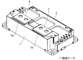
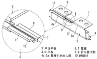
本発明の実施の形態1について、図面を用いて以下に説明する。図1は、実施の形態1に係る半導体装置の斜視図であり、図2は、実施の形態1に係る半導体装置の平行平板3および電極6,7の斜視図である。
<
図1と図2に示すように、半導体装置は、IGBTモジュールまたはSiCモジュールなどのパワーモジュールであり、樹脂ケース1、平行平板3および電極6,7を備えている。樹脂ケース1は箱状に形成され、内部に半導体素子(図示省略)が収容されている。樹脂ケース1において前部の上面が後部の上面よりも高い高さ位置になるように形成されている。樹脂ケース1の後部の上端部に蓋2が配置され、蓋2が樹脂ケース1の後部の上面を形成している。
As shown in FIGS. 1 and 2, the semiconductor device is a power module such as an IGBT module or a SiC module, and includes a
平行平板3は、半導体素子と接続されるとともに樹脂ケース1の前部の内部に配置されている。平行平板3は、絶縁材10を介して互いに平行に配置される2枚の平板4,5によって構成されている。平板4は、樹脂ケース1の幅方向に延びるように形成され、主面が前方または後方を向くように配置されている。平板4の幅方向左端部の上端(電極引き出し部4a)から後方に向けて電極6が引き出されている。平板5は、樹脂ケース1の幅方向に延びるように形成され、主面が前方または後方を向くように配置されている。平板5の幅方向右端部の上端(電極引き出し部5a)から後方に向けて電極7が引き出されている。電極6および電極7は、樹脂ケース1の前部の上面に予め定められた間隔をあけて配置されている。
The parallel plate 3 is connected to the semiconductor element and disposed inside the front portion of the
平行平板3における2つの電極引き出し部4a,5aの間の上端部に、それぞれ互いに遠ざかる方向である外側に曲げられた折り曲げ部8,9が設けられている。折り曲げ部8,9によって、平行平板3における2つの電極引き出し部4a,5aの間の上端部の厚みを増すことで、この部分の磁束の集中を緩和し、半導体装置の自己インダクタンスを低減可能としている。
Bending
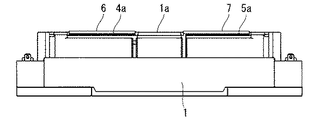
次に、樹脂ケース1の前部の上面の構造について説明する。図3は、実施の形態1に係る半導体装置の電極引き出し部4a,5aの間を示す拡大斜視図であり、図4は、実施の形態1に係る半導体装置の正面図であり、図5は、実施の形態1に係る半導体装置の上端部を示す拡大正面図である。
Next, the structure of the upper surface of the front part of the
図3に示すように、樹脂ケース1の上面における電極引き出し部4a,5aの間の部分に対応する領域1aは、平面状に形成されている。より具体的には、樹脂ケース1の前部の前側部分の上面は前部の後側部分の上面よりも高い高さ位置に形成され、領域1aは、樹脂ケース1の前部の前側部分の上面における電極引き出し部4a,5aの間の部分に対応する領域である。なお、樹脂ケース1の前部の後側部分の上面における電極引き出し部4a,5aの間の部分に対応する領域も平面状に形成されている。ここで、平行平板3は、樹脂ケース1の前部の前側部分の内部に収容されている。電極引き出し部4a,5aに外部の平行平板配線(ブスバー)が接続されるが、領域1aが平面状に形成されているため、平行平板3における電極引き出し部4a,5aの間の部分とブスバーとの距離を近づけることができる。
As shown in FIG. 3, the
単純に考えると電極引き出し部4a,5a同士を近づけた方が半導体装置の自己インダクタンスを低減できるように感じるが、本願の発明者は、詳細に電磁界シミュレーションを繰り返した結果、電極引き出し部4a,5aの間の距離を近づけた場合よりも、平行平板3における電極引き出し部4a,5aの間の部分とブスバーとの距離を近づけた場合の方が半導体装置の自己インダクタンスを低減できるとの知見を得た。このためには、樹脂ケース1の上面における電極引き出し部4a,5aの間の部分に対応する領域1aには沿面距離を稼ぐための凹凸形状がない方が良い。
If it thinks simply, it will feel that the electrode lead-out
図4と図5に示すように、樹脂ケース1の前部の前側部分の上面における電極引き出し部4a,5aの間の部分に対応する領域1aは、電極6,7の上面と下面の間の高さ位置に位置している。樹脂ケース1の前部の前側部分の内部において平行平板3を上方に配置することができるため、平行平板3における電極引き出し部4a,5aの間の部分とブスバーとの距離を近づけることができる。ここで、樹脂ケース1の上面における電極引き出し部4a,5aの間の部分に対応する領域1a、すなわち、平行平板3における電極引き出し部4a,5aの間を覆う樹脂ケース1の部分の高さ位置は、ブスバーの取り付け公差の許す範囲内で高くする方が好ましい。
As shown in FIGS. 4 and 5, a
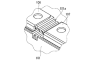
次に、実施の形態1に係る半導体装置から得られる効果について、前提技術に係る半導体装置の場合と対比しながら説明する。図10は、前提技術に係る半導体装置の斜視図であり、図11は、前提技術に係る半導体装置の平行平板103および電極106,107の斜視図であり、図12は、前提技術に係る半導体装置の電極引き出し部104a,105aの間を示す拡大斜視図である。
Next, effects obtained from the semiconductor device according to the first embodiment will be described in comparison with the semiconductor device according to the base technology. 10 is a perspective view of the semiconductor device according to the base technology, FIG. 11 is a perspective view of the
最初に、前提技術に係る半導体装置について説明する。図10と図11に示すように、前提技術に係る半導体装置は、樹脂ケース101、平行平板103および電極106,107を備えている。樹脂ケース101の後部の上端部に蓋102が配置され、蓋102が樹脂ケース101の後部の上面を形成している。
First, a semiconductor device according to the prerequisite technology will be described. As shown in FIGS. 10 and 11, the semiconductor device according to the base technology includes a
平行平板103は、半導体素子と接続されるとともに樹脂ケース101の前部の内部に配置されている。平行平板103は、絶縁材10を介して互いに平行に配置される2枚の平板104,105によって構成されている。平板104は、樹脂ケース101の幅方向に延びるように形成され、主面が前方または後方を向くように配置されている。平板104の幅方向左端部の上端(電極引き出し部104a)から後方に向けて電極106が引き出されている。平板105は、樹脂ケース101の幅方向に延びるように形成され、主面が前方または後方を向くように配置されている。平板105の幅方向右端部の上端(電極引き出し部105a)から後方に向けて電極107が引き出されている。電極106および電極107は、樹脂ケース101の前部の上面に予め定められた間隔をあけて配置されている。
The
ここで、前提技術においては、電極106と電極107との間隔は、実施の形態1の場合と比較して狭くなっている。これは、平行平板103における電極引き出し部104a,105aの間の間隔が狭い方が半導体装置の自己インダクタンスを低減させることができるからである。
Here, in the base technology, the distance between the
しかし、図10と図12に示すように、前提技術に係る半導体装置では、電極106と電極107との間の沿面距離を稼ぐために、樹脂ケース101の上面における電極引き出し部104a,105aの間の部分に対応する領域101aは凹凸形状に形成されている。そのため、平行平板103における電極引き出し部104a,105aの間の部分と、電極引き出し部104a,105aに接続されるブスバーとの距離が長くなり、自己インダクタンスを一定以上低減させることが困難であった。
However, as shown in FIGS. 10 and 12, in the semiconductor device according to the base technology, in order to increase the creepage distance between the
これに対して、実施の形態1に係る半導体装置は、図2に示すように、平行平板3における2つの電極6,7がそれぞれ引き出される2つの電極引き出し部4a,5aの間の上端部はそれぞれ互いに遠ざかる方向である外側に曲げられるため、平行平板3における2つの電極引き出し部4a,5aの間の上端部の厚みが増す。平行平板3の上下方向の端部は磁束が集中し易いが、平行平板3における2つの電極引き出し部4a,5aの間の上端部の厚みを増すことで、この部分の磁束の集中が緩和され、半導体装置の自己インダクタンスを低減させることができる。
In contrast, in the semiconductor device according to the first embodiment, as shown in FIG. 2, the upper end portion between the two
図3に示すように、樹脂ケース1の上面における2つの電極引き出し部4a,5aの間の部分に対応する領域1aは、平面状に形成されるため、平行平板3における電極引き出し部4a,5aの間の部分とブスバーとの距離を短くすることができ、半導体装置の自己インダクタンスを低減させることができる。
As shown in FIG. 3, since the
図4と図5に示すように、樹脂ケース1の上面における2つの電極引き出し部4a,5aの間の部分に対応する領域1aは、2つの電極6,7の上面と下面の間の高さ位置に位置するため、平行平板3における電極引き出し部4a,5aの間の部分とブスバーとの距離を短くすることができ、半導体装置の自己インダクタンスを低減させることができる。
As shown in FIGS. 4 and 5, the
<実施の形態2>
次に、実施の形態2に係る半導体装置について説明する。図6は、実施の形態2に係る半導体装置の平行平板3および電極6,7の斜視図である。なお、実施の形態2において、実施の形態1で説明したものと同一の構成要素については同一符号を付して説明は省略する。
<
Next, a semiconductor device according to the second embodiment will be described. FIG. 6 is a perspective view of parallel plate 3 and
図6に示すように、実施の形態2では、平行平板3における2つの電極引き出し部4a,5aの間の上部同士の間隔は、2つの電極引き出し部4a,5aの間の上部以外の部分同士の間隔よりも広い。より具体的には、平行平板3を構成する平板5における電極引き出し部4a,5aの間の上部に、互いに遠ざかる方向である外側に張り出す張り出し部12が設けられているため、平行平板3における電極引き出し部4a,5aの間の上部同士の間隔がそれ以外の部分同士の間隔よりも広くなっている。これにより、平板5における電極引き出し部4a,5aの間の上部の厚みが増すことと同様の効果が得られる。ここで、張り出し部12は絞り加工によって形成されている。なお、平板5に張り出し部12を設ける代わりに、平板4における電極引き出し部4a,5aの間の上部に、互いに遠ざかる方向である外側に張り出す張り出し部を設けても良い。
As shown in FIG. 6, in the second embodiment, the interval between the upper portions between the two
以上のように、実施の形態2に係る半導体装置では、平行平板3における2つの電極引き出し部4a,5aの間の上部同士の間隔は、2つの電極引き出し部4a,5aの間の上部以外の部分同士の間隔よりも広いため、平行平板3における2つの電極引き出し部4a,5aの間の上部の厚みが増すことと同様の効果が得られる。これにより、半導体装置の自己インダクタンスを低減させることができる。
As described above, in the semiconductor device according to the second embodiment, the interval between the upper portions between the two
ここで、実施の形態1の場合のように、平行平板3における電極引き出し部4a,5aの間の上端部をそれぞれ互いに遠ざかる方向である外側に曲げるためには曲げ方向にある程度の長さが必要であるため、平行平板3における電極引き出し部4a,5aの間の上端部が大きくなってしまう。また、樹脂ケース1の内部に平行平板3を配置するために一般にインサート成型が使用されるが、インサート圧力によって電極6,7の端部が変形し互いに接近しやすくなる。そこで、平行平板3において概ね平行を保ちながら電極引き出し部4a,5aの間の上部の間隔を広げることで、実施の形態1の場合よりも平行平板3における電極引き出し部4a,5aの間の上端部をコンパクトな形状にすることができるとともに、優れた成型性が得られる。
Here, as in the case of the first embodiment, in order to bend the upper end portions between the
張り出し部12は、絞り加工によって形成されるため、張り出し部12を簡単に実現することができる。
Since the
<実施の形態3>
次に、実施の形態3に係る半導体装置について説明する。図7は、実施の形態3に係る半導体装置の平行平板3および電極6,7の斜視図であり、図8は、実施の形態3に係る半導体装置の平行平板3における電極引き出し部4a,5aの間を示す平面図である。なお、実施の形態3において、実施の形態1,2で説明したものと同一の構成要素については同一符号を付して説明は省略する。
<Embodiment 3>
Next, a semiconductor device according to the third embodiment will be described. 7 is a perspective view of the parallel plate 3 and the
図7と図8に示すように、実施の形態3では、張り出し部11は、平板4における電極引き出し部4a,5aの間の上部に設けられるとともに、張り出し部12は、平板5における電極引き出し部4a,5aの間の上部に設けられている。そのため、平行平板3における電極引き出し部4a,5aの間の上部同士の間隔がそれ以外の部分同士の間隔よりも広くなっている。ここで、実施の形態2の場合と同様に、張り出し部11,12は絞り加工によって形成されている。
As shown in FIGS. 7 and 8, in the third embodiment, the overhanging
以上のように、実施の形態3に係る半導体装置では、平行平板3を構成する2枚の平板4,5の両方における2つの電極引き出し部4a,5aの間の上部に、互いに遠ざかる方向である外側に張り出す張り出し部11,12が設けられるため、平行平板3における電極引き出し部4a,5aの間の上部の厚みが増すことと同様の効果が得られ、半導体装置の自己インダクタンスを低減させることができる。さらに、樹脂ケース1および平行平板3をインサート成型する際に樹脂の流動圧力が均等化されるという効果も得られる。
As described above, in the semiconductor device according to the third embodiment, the distance between the two
<実施の形態4>
次に、実施の形態4に係る半導体装置について説明する。図9は、実施の形態4に係る半導体装置の平行平板3および電極6,7の斜視図である。なお、実施の形態4において、実施の形態1から実施の形態3で説明したものと同一の構成要素については同一符号を付して説明は省略する。
<Embodiment 4>
Next, a semiconductor device according to the fourth embodiment will be described. FIG. 9 is a perspective view of parallel plate 3 and
図9に示すように、実施の形態4では、張り出し部11,12に張り出し部11,12を複数に分割する分割部13が設けられている。より具体的には、分割部13は、上下方向に延びるスリット状に形成され、張り出し部11,12を幅方向に複数に分割している。なお、分割部13は、張り出し部11,12の一方にのみ設けられていても良い。
As shown in FIG. 9, in the fourth embodiment, the overhanging
以上のように、実施の形態4に係る半導体装置では、張り出し部11,12に当該張り出し部11,12を複数に分割する分割部13が設けられるため、樹脂ケース1および平行平板3をインサート成型する際に樹脂の流動性が向上する。
As described above, in the semiconductor device according to the fourth embodiment, since the projecting
なお、本発明は、その発明の範囲内において、各実施の形態を自由に組み合わせたり、各実施の形態を適宜、変形、省略することが可能である。 It should be noted that the present invention can be freely combined with each other within the scope of the invention, and each embodiment can be appropriately modified or omitted.
1 樹脂ケース、3 平行平板、4,5 平板、4a,5a 電極引き出し部、6,7 電極、8,9 折り曲げ部、10 絶縁材、11,12 張り出し部、13 分割部。
DESCRIPTION OF
Claims (7)
前記半導体素子と接続されるとともに前記樹脂ケース内に配置され、かつ、絶縁材を介して互いに平行に配置される2枚の平板によって構成される平行平板と、
前記平行平板の上端からそれぞれ引き出されて前記樹脂ケースの上面に予め定められた間隔をあけて配置される2つの電極と、
を備え、
前記平行平板における前記2つの電極がそれぞれ引き出される2つの電極引き出し部の間の上端部はそれぞれ互いに遠ざかる方向である外側に曲げられる、半導体装置。 A resin case for housing a semiconductor element;
A parallel flat plate constituted by two flat plates connected to the semiconductor element and arranged in the resin case and arranged in parallel with each other through an insulating material;
Two electrodes that are respectively drawn from the upper ends of the parallel plates and arranged on the upper surface of the resin case with a predetermined interval;
With
A semiconductor device, wherein an upper end portion between two electrode lead portions from which the two electrodes are drawn out from the parallel plate is bent outward, which is a direction away from each other.
前記半導体素子と接続されるとともに前記樹脂ケース内に配置され、かつ、絶縁材を介して互いに平行に配置される2枚の平板によって構成される平行平板と、
前記平行平板の上端からそれぞれ引き出されて前記樹脂ケースの上面に予め定められた間隔をあけて配置される2つの電極と、
を備え、
前記平行平板における前記2つの電極がそれぞれ引き出される2つの電極引き出し部の間の上部同士の間隔は、前記2つの電極引き出し部の間の上部以外の部分同士の間隔よりも広い、半導体装置。 A resin case for housing a semiconductor element;
A parallel flat plate constituted by two flat plates connected to the semiconductor element and arranged in the resin case and arranged in parallel with each other through an insulating material;
Two electrodes that are respectively drawn from the upper ends of the parallel plates and arranged on the upper surface of the resin case with a predetermined interval;
With
The semiconductor device, wherein an interval between upper portions between two electrode lead portions from which the two electrodes are drawn out in the parallel plate is wider than a gap between portions other than the upper portion between the two electrode lead portions.
前記張り出し部に当該張り出し部を複数に分割する分割部が設けられる、請求項2記載の半導体装置。 In the upper part between the two electrode lead portions in at least one of the two flat plates constituting the parallel flat plate, an overhanging portion that protrudes outward is provided in a direction away from each other.
The semiconductor device according to claim 2, wherein the projecting part is provided with a dividing unit that divides the projecting part into a plurality of parts.
前記張り出し部は、絞り加工によって形成される、請求項2記載の半導体装置。 In the upper part between the two electrode lead portions in at least one of the two flat plates constituting the parallel flat plate, an overhanging portion that protrudes outward is provided in a direction away from each other.
The semiconductor device according to claim 2, wherein the protruding portion is formed by drawing.
Priority Applications (4)
| Application Number | Priority Date | Filing Date | Title |
|---|---|---|---|
| JP2015062241A JP6300751B2 (en) | 2015-03-25 | 2015-03-25 | Semiconductor device |
| US14/926,805 US9627284B2 (en) | 2015-03-25 | 2015-10-29 | Semiconductor device |
| DE102015222826.6A DE102015222826B4 (en) | 2015-03-25 | 2015-11-19 | Semiconductor device |
| CN201610177520.9A CN106024748B (en) | 2015-03-25 | 2016-03-25 | Semiconductor device |
Applications Claiming Priority (1)
| Application Number | Priority Date | Filing Date | Title |
|---|---|---|---|
| JP2015062241A JP6300751B2 (en) | 2015-03-25 | 2015-03-25 | Semiconductor device |
Publications (3)
| Publication Number | Publication Date |
|---|---|
| JP2016181649A JP2016181649A (en) | 2016-10-13 |
| JP2016181649A5 JP2016181649A5 (en) | 2017-06-29 |
| JP6300751B2 true JP6300751B2 (en) | 2018-03-28 |
Family
ID=56890275
Family Applications (1)
| Application Number | Title | Priority Date | Filing Date |
|---|---|---|---|
| JP2015062241A Active JP6300751B2 (en) | 2015-03-25 | 2015-03-25 | Semiconductor device |
Country Status (4)
| Country | Link |
|---|---|
| US (1) | US9627284B2 (en) |
| JP (1) | JP6300751B2 (en) |
| CN (1) | CN106024748B (en) |
| DE (1) | DE102015222826B4 (en) |
Families Citing this family (17)
| Publication number | Priority date | Publication date | Assignee | Title |
|---|---|---|---|---|
| JP6399962B2 (en) * | 2015-04-16 | 2018-10-03 | 三菱電機株式会社 | Semiconductor device |
| USD814431S1 (en) * | 2015-05-15 | 2018-04-03 | Mitsubishi Electric Corporation | Power semiconductor device |
| JP1585831S (en) | 2017-01-05 | 2017-09-11 | ||
| USD864132S1 (en) | 2017-01-05 | 2019-10-22 | Rohm Co., Ltd. | Power semiconductor module |
| JP1603980S (en) * | 2017-09-07 | 2018-05-14 | ||
| JP1603793S (en) * | 2017-09-29 | 2018-05-14 | ||
| JP1632173S (en) * | 2018-06-01 | 2019-05-27 | ||
| JP1659675S (en) | 2019-08-29 | 2020-05-18 | ||
| JP1659673S (en) | 2019-08-29 | 2020-05-18 | ||
| JP1659677S (en) | 2019-08-29 | 2020-05-18 | ||
| JP1659678S (en) | 2019-08-29 | 2020-05-18 | ||
| JP1659716S (en) | 2019-08-29 | 2020-05-18 | ||
| JP1659676S (en) | 2019-08-29 | 2020-05-18 | ||
| JP1659674S (en) | 2019-08-29 | 2020-05-18 | ||
| JP1659672S (en) * | 2019-08-29 | 2020-05-18 | ||
| USD916039S1 (en) * | 2020-03-20 | 2021-04-13 | Sansha Electric Manufacturing Co., Ltd. | Semiconductor device |
| DE102020124149A1 (en) | 2020-09-16 | 2022-03-17 | Danfoss Silicon Power Gmbh | power module |
Family Cites Families (16)
| Publication number | Priority date | Publication date | Assignee | Title |
|---|---|---|---|---|
| US5523620A (en) * | 1994-02-14 | 1996-06-04 | Delco Electronics Corporation | Coplanar linear dual switch module |
| JPH0783087B2 (en) | 1994-04-19 | 1995-09-06 | 富士電機株式会社 | Semiconductor device |
| JP3997730B2 (en) * | 2001-06-20 | 2007-10-24 | 株式会社日立製作所 | Power conversion apparatus and moving body equipped with the same |
| JP4081611B2 (en) | 2003-11-19 | 2008-04-30 | 株式会社豊田自動織機 | Semiconductor device |
| JP4566678B2 (en) * | 2004-10-04 | 2010-10-20 | 日立オートモティブシステムズ株式会社 | Power module |
| JP4660214B2 (en) * | 2005-01-26 | 2011-03-30 | 日本インター株式会社 | Power semiconductor device |
| JP4603956B2 (en) * | 2005-08-26 | 2010-12-22 | 日立オートモティブシステムズ株式会社 | Power converter |
| JP4410241B2 (en) * | 2006-12-27 | 2010-02-03 | 三菱電機株式会社 | Electronic control unit |
| JP4865829B2 (en) * | 2009-03-31 | 2012-02-01 | シャープ株式会社 | Semiconductor device and manufacturing method thereof |
| EP3633723B1 (en) * | 2009-05-14 | 2023-02-22 | Rohm Co., Ltd. | Semiconductor device |
| WO2011016360A1 (en) * | 2009-08-03 | 2011-02-10 | 株式会社安川電機 | Power converter |
| JP5418668B2 (en) * | 2010-03-16 | 2014-02-19 | 富士電機株式会社 | Semiconductor device |
| JP5555206B2 (en) | 2011-07-11 | 2014-07-23 | 株式会社 日立パワーデバイス | Semiconductor power module |
| CN103733333B (en) * | 2011-09-28 | 2017-04-12 | 富士电机株式会社 | Semiconductor device and method for producing semiconductor device |
| CN104303297B (en) * | 2012-05-16 | 2017-05-17 | 松下知识产权经营株式会社 | Power semiconductor module |
| JP2014086506A (en) * | 2012-10-22 | 2014-05-12 | Toyota Motor Corp | Semiconductor device |
-
2015
- 2015-03-25 JP JP2015062241A patent/JP6300751B2/en active Active
- 2015-10-29 US US14/926,805 patent/US9627284B2/en active Active
- 2015-11-19 DE DE102015222826.6A patent/DE102015222826B4/en active Active
-
2016
- 2016-03-25 CN CN201610177520.9A patent/CN106024748B/en active Active
Also Published As
| Publication number | Publication date |
|---|---|
| US20160284618A1 (en) | 2016-09-29 |
| US9627284B2 (en) | 2017-04-18 |
| CN106024748B (en) | 2018-11-23 |
| DE102015222826A1 (en) | 2016-09-29 |
| JP2016181649A (en) | 2016-10-13 |
| DE102015222826B4 (en) | 2021-08-12 |
| CN106024748A (en) | 2016-10-12 |
Similar Documents
| Publication | Publication Date | Title |
|---|---|---|
| JP6300751B2 (en) | Semiconductor device | |
| JP2016046384A (en) | Semiconductor device | |
| JP6451747B2 (en) | Semiconductor device | |
| JP5136343B2 (en) | Semiconductor device | |
| CN105099252B (en) | power semiconductor device | |
| US10021802B2 (en) | Electronic module assembly having low loop inductance | |
| CN107393715A (en) | Capacitor, the intermediate circuit particularly for multiphase system | |
| JP5776707B2 (en) | Semiconductor device | |
| JP5481104B2 (en) | Semiconductor device | |
| US10536090B2 (en) | Bus bar structure and power conversion device using same | |
| JPWO2017122471A1 (en) | Semiconductor device | |
| US10062633B2 (en) | Substrate unit | |
| US20150262915A1 (en) | Semiconductor device and module | |
| JP6123722B2 (en) | Semiconductor device | |
| JP6277292B1 (en) | Semiconductor device and lead frame | |
| JP6481505B2 (en) | Power converter | |
| JP2013102242A (en) | Power semiconductor device | |
| JP5544767B2 (en) | Semiconductor device | |
| JP6402280B2 (en) | Electronics | |
| US9991180B2 (en) | Semiconductor device for reducing self-inductance | |
| CN114616639B (en) | capacitor | |
| JP2009259990A (en) | Semiconductor module | |
| JP2017073948A (en) | Power converter | |
| JP6325757B1 (en) | Electronic equipment | |
| JP7253684B2 (en) | inductor |
Legal Events
| Date | Code | Title | Description |
|---|---|---|---|
| A521 | Request for written amendment filed |
Free format text: JAPANESE INTERMEDIATE CODE: A523 Effective date: 20170515 |
|
| A621 | Written request for application examination |
Free format text: JAPANESE INTERMEDIATE CODE: A621 Effective date: 20170515 |
|
| A977 | Report on retrieval |
Free format text: JAPANESE INTERMEDIATE CODE: A971007 Effective date: 20180122 |
|
| TRDD | Decision of grant or rejection written | ||
| A01 | Written decision to grant a patent or to grant a registration (utility model) |
Free format text: JAPANESE INTERMEDIATE CODE: A01 Effective date: 20180130 |
|
| A61 | First payment of annual fees (during grant procedure) |
Free format text: JAPANESE INTERMEDIATE CODE: A61 Effective date: 20180227 |
|
| R150 | Certificate of patent or registration of utility model |
Ref document number: 6300751 Country of ref document: JP Free format text: JAPANESE INTERMEDIATE CODE: R150 |
|
| R250 | Receipt of annual fees |
Free format text: JAPANESE INTERMEDIATE CODE: R250 |
|
| R250 | Receipt of annual fees |
Free format text: JAPANESE INTERMEDIATE CODE: R250 |
|
| R250 | Receipt of annual fees |
Free format text: JAPANESE INTERMEDIATE CODE: R250 |
|
| R250 | Receipt of annual fees |
Free format text: JAPANESE INTERMEDIATE CODE: R250 |
|
| R250 | Receipt of annual fees |
Free format text: JAPANESE INTERMEDIATE CODE: R250 |
|
| R250 | Receipt of annual fees |
Free format text: JAPANESE INTERMEDIATE CODE: R250 |