JP6295210B2 - Power system - Google Patents
Power system Download PDFInfo
- Publication number
- JP6295210B2 JP6295210B2 JP2015010269A JP2015010269A JP6295210B2 JP 6295210 B2 JP6295210 B2 JP 6295210B2 JP 2015010269 A JP2015010269 A JP 2015010269A JP 2015010269 A JP2015010269 A JP 2015010269A JP 6295210 B2 JP6295210 B2 JP 6295210B2
- Authority
- JP
- Japan
- Prior art keywords
- power
- reactor
- current
- power supply
- duty ratio
- Prior art date
- Legal status (The legal status is an assumption and is not a legal conclusion. Google has not performed a legal analysis and makes no representation as to the accuracy of the status listed.)
- Active
Links
- 230000001172 regenerating effect Effects 0.000 claims description 37
- 238000006243 chemical reaction Methods 0.000 claims description 31
- 230000007423 decrease Effects 0.000 claims description 24
- 230000004044 response Effects 0.000 claims description 10
- 238000007599 discharging Methods 0.000 claims description 4
- 238000010586 diagram Methods 0.000 description 38
- 230000000630 rising effect Effects 0.000 description 20
- 230000004048 modification Effects 0.000 description 16
- 238000012986 modification Methods 0.000 description 16
- 239000004065 semiconductor Substances 0.000 description 12
- 230000000295 complement effect Effects 0.000 description 10
- 230000014509 gene expression Effects 0.000 description 10
- 230000015572 biosynthetic process Effects 0.000 description 4
- 239000003990 capacitor Substances 0.000 description 3
- HBBGRARXTFLTSG-UHFFFAOYSA-N Lithium ion Chemical compound [Li+] HBBGRARXTFLTSG-UHFFFAOYSA-N 0.000 description 2
- 230000002457 bidirectional effect Effects 0.000 description 2
- 238000001514 detection method Methods 0.000 description 2
- 230000000694 effects Effects 0.000 description 2
- 229910001416 lithium ion Inorganic materials 0.000 description 2
- 239000000470 constituent Substances 0.000 description 1
- 230000006870 function Effects 0.000 description 1
- 229910052987 metal hydride Inorganic materials 0.000 description 1
- 229910044991 metal oxide Inorganic materials 0.000 description 1
- 150000004706 metal oxides Chemical class 0.000 description 1
- 229910052759 nickel Inorganic materials 0.000 description 1
- PXHVJJICTQNCMI-UHFFFAOYSA-N nickel Substances [Ni] PXHVJJICTQNCMI-UHFFFAOYSA-N 0.000 description 1
- -1 nickel metal hydride Chemical class 0.000 description 1
- 238000010248 power generation Methods 0.000 description 1
Images

Landscapes
- Dc-Dc Converters (AREA)
Description
この発明は、電源システムに関し、より特定的には、2つの直流電源と負荷との間で直流電力変換を実行するための電源システムに関する。 The present invention relates to a power supply system, and more particularly to a power supply system for executing DC power conversion between two DC power supplies and a load.
複数の電源と負荷との間に接続された電力変換器を用いて、複数の電源を組み合わせて負荷へ電力を供給するハイブリッド電源システムが用いられている。 A hybrid power supply system that uses a power converter connected between a plurality of power supplies and a load to supply power to the load by combining the plurality of power supplies is used.
たとえば、特開2013−13234号公報(特許文献1)には、複数のスイッチング素子のスイッチングパターンを切換えることによって、動作モードを切換えることが可能な電力変換器の構成が記載されている。そして、動作モードには、2つの直流電源を並列に使用する状態で直流電力変換を行なうモード(並列接続モード)が含まれる。 For example, Japanese Patent Laying-Open No. 2013-13234 (Patent Document 1) describes a configuration of a power converter that can switch an operation mode by switching switching patterns of a plurality of switching elements. The operation mode includes a mode (parallel connection mode) in which DC power conversion is performed in a state where two DC power supplies are used in parallel.
特許文献1に記載された電力変換器では、並列接続モードにおいて、2つの直流電源からの直流電源変換は、電流経路を共有する複数のスイッチング素子によってそれぞれ制御される。特許文献1では、第1の直流電源からの直流電力変換を制御するためのPWM(Pulse Width Modulation)制御に使用される第1のキャリア波と、第2の直流電源からの直流電力変換を制御するためのPWM制御に使用される第2のキャリア波との位相差を調整することによって、複数のスイッチング素子のスイッチング損失の低減を図っている。しかしながら、第1および第2のキャリア波間の位相差を調整するのみでは、スイッチング損失の低減効果に限界がある。
In the power converter described in
この発明は、このような問題点を解決するためになされたものであって、その目的は、2つの直流電源を備えた電源システムのスイッチング損失を低減して、直流電力変換を高効率化することである。 The present invention has been made to solve such problems, and its object is to reduce the switching loss of a power supply system having two DC power supplies and to improve the efficiency of DC power conversion. That is.
この発明のある局面では、高電圧側の第1の電力線および低電圧側の第2の電力線の間の直流電圧を制御するための電源システムは、第1の直流電源と、第2の直流電源と、第1および第2の直流電源と第1および第2の電力線との間で並列に直流電力変換を実行するための電力変換器と、電力変換器における直流電圧変換を制御するための制御装置を備える。電力変換器は、第1のリアクトルと、第2のリアクトルと、制御装置からの制御信号に応答して、第1の直流電源と第1および第2の電力線との間に、第1のリアクトルにエネルギを蓄積するための第1の電流経路および第1のリアクトルのエネルギを放出するための第2の電流経路を交互に形成するとともに、第2の直流電源と第1および第2の電力線との間に、第2のリアクトルにエネルギを蓄積するための第3の電流経路および第2のリアクトルのエネルギを放出するための第4の電流経路を交互に形成するように構成された複数のスイッチング素子とを含む。複数のスイッチング素子の各々は、第1および第2の電流経路のいずれか一方と、第3および第4の電流経路のいずれか一方との両方に含まれるように配置される。制御装置は、m個(mは2以上の整数)のキャリア周期を1調整期間として、当該1調整期間内の各キャリア周期において、第1の直流電源からの第1の出力デューティ比と第1のキャリア波との比較による第1のパルス幅変調制御を実行するとともに、第2の直流電源からの第2の出力デューティ比と第2のキャリア波との比較による第2のパルス幅変調制御を実行する。複数のスイッチング素子は、第1のパルス幅変調制御に従って第1のリアクトルの電流の増減が制御されるとともに、第2のパルス幅変調制御に従って第2のリアクトルの電流の増減が制御されるように、制御信号に従ってオンオフされる。m個のキャリア周期は、n個(nは1以上m未満の整数)の第1のキャリア周期と、(m−n)個の第2のキャリア周期とから構成される。第1のキャリア周期において、制御装置は、第1のリアクトルの電流の2つの変曲点と第2のリアクトルの電流の2つの変曲点とがそれぞれ同一タイミングとなるように、第1および第2の出力デューティ比を調整するとともに、第1のキャリア波および第2のキャリア波の間の位相差を調整する。第2のキャリア周期において、制御装置は、第1のキャリア周期における第1および第2の出力デューティ比に基づいて第1および第2の出力デューティ比を調整し、さらに、第1のリアクトルの電流の2つの変曲点の一方と第2のリアクトルの電流の2つの変曲点の一方とが同一タイミングとなるように、位相差を調整する。 In one aspect of the present invention, a power supply system for controlling a DC voltage between a first power line on a high voltage side and a second power line on a low voltage side includes a first DC power supply and a second DC power supply. A power converter for executing DC power conversion in parallel between the first and second DC power supplies and the first and second power lines, and a control for controlling DC voltage conversion in the power converter Equipment. In response to a control signal from the first reactor, the second reactor, and the control device, the power converter includes a first reactor between the first DC power source and the first and second power lines. And alternately forming a first current path for storing energy and a second current path for discharging energy of the first reactor, and a second DC power source, first and second power lines, A plurality of switching devices configured to alternately form a third current path for storing energy in the second reactor and a fourth current path for discharging energy of the second reactor during Element. Each of the plurality of switching elements is arranged to be included in both one of the first and second current paths and either one of the third and fourth current paths. The control device takes m carrier cycles (m is an integer of 2 or more) as one adjustment period, and sets the first output duty ratio from the first DC power source and the first in each carrier period within the one adjustment period. The first pulse width modulation control based on the comparison with the second carrier wave is executed, and the second pulse width modulation control based on the comparison between the second output duty ratio from the second DC power source and the second carrier wave is performed. Run. The plurality of switching elements are controlled so as to increase or decrease the current of the first reactor according to the first pulse width modulation control, and to control the increase or decrease of the current of the second reactor according to the second pulse width modulation control. , On and off according to the control signal. The m carrier periods are composed of n (n is an integer greater than or equal to 1 and less than m) first carrier periods and (mn) second carrier periods. In the first carrier cycle, the control device sets the first and second inflection points so that the two inflection points of the current of the first reactor and the two inflection points of the current of the second reactor have the same timing, respectively. The output duty ratio of 2 is adjusted, and the phase difference between the first carrier wave and the second carrier wave is adjusted. In the second carrier period, the control device adjusts the first and second output duty ratios based on the first and second output duty ratios in the first carrier period, and further, the current of the first reactor The phase difference is adjusted so that one of the two inflection points and one of the two inflection points of the current of the second reactor have the same timing.
好ましくは、第2のキャリア周期において、制御装置は、1調整期間を通算した第1の出力デューティ比の平均値が、第1の直流電源からの出力を制御するためのデューティ比に相当するとともに、1調整期間を通算した第2の出力デューティ比の平均値が、第2の直流電源からの出力を制御するためのデューティ比に相当するように、第1のキャリア周期における第1および第2の出力デューティ比に基づいて、第1および第2の出力デューティ比を調整する。 Preferably, in the second carrier cycle, the control device is configured such that the average value of the first output duty ratio for one adjustment period corresponds to the duty ratio for controlling the output from the first DC power supply. 1st and 2nd in the 1st carrier cycle so that the average value of the 2nd output duty ratio which added up 1 adjustment period may correspond to the duty ratio for controlling the output from the 2nd direct-current power supply. The first and second output duty ratios are adjusted based on the output duty ratio.
好ましくは、第1のキャリア周期において、制御装置は、第1の直流電源が力行および回生のいずれの状態であるか、および、第2の直流電源が力行および回生のいずれの状態であるかの組合せに基づいて、第1および第2の出力デューティ比を調整するとともに、第1のキャリア波および第2のキャリア波の間の位相差を調整する。 Preferably, in the first carrier cycle, the control device determines whether the first DC power source is in a power running state or a regenerative state, and whether the second DC power source is in a power running state or a regenerative state. Based on the combination, the first and second output duty ratios are adjusted, and the phase difference between the first carrier wave and the second carrier wave is adjusted.
好ましくは、第1の直流電源および第2の直流電源が力行状態である場合、または、第1の直流電源および第2の直流電源が回生状態である場合には、制御装置は、第1のキャリア周期において、第1の電流経路から第2の電流経路へ切換えるときの第1のリアクトルの電流の変曲点と、第4の電流経路から第3の電流経路へ切換えるときの第2のリアクトルの電流の変曲点とが同一タイミングとなり、かつ、第2の電流経路から第1の電流経路へ切換えるときの第1のリアクトルの電流の変曲点と、第3の電流経路から第4の電流経路へ切換えるときの第2のリアクトルの電流の変曲点とが同一タイミングとなるように、第1および第2の出力デューティ比を調整するとともに、位相差を調整する。 Preferably, when the first DC power source and the second DC power source are in a power running state, or when the first DC power source and the second DC power source are in a regenerative state, the control device includes: In the carrier cycle, the inflection point of the current of the first reactor when switching from the first current path to the second current path, and the second reactor when switching from the fourth current path to the third current path The inflection point of the current of the first reactor and the inflection point of the current of the first reactor when switching from the second current path to the first current path, and the fourth from the third current path. The first and second output duty ratios are adjusted and the phase difference is adjusted so that the inflection point of the current of the second reactor when switching to the current path is at the same timing.
好ましくは、第1の直流電源および第2の直流電源が力行状態である場合、または、第1の直流電源および第2の直流電源が回生状態である場合には、制御装置は、第1のキャリア周期において、第1の出力デューティ比と第2の出力デューティ比との和が1となるように、第1および第2の出力デューティ比を調整するとともに、位相差を180度に調整する。 Preferably, when the first DC power source and the second DC power source are in a power running state, or when the first DC power source and the second DC power source are in a regenerative state, the control device includes: In the carrier period, the first and second output duty ratios are adjusted and the phase difference is adjusted to 180 degrees so that the sum of the first output duty ratio and the second output duty ratio becomes 1.
好ましくは、第1の直流電源が回生状態であり、かつ、第2の直流電源が力行状態である場合、または、第1の直流電源が力行状態であり、かつ、第2の直流電源が回生状態である場合には、制御装置は、第1のキャリア周期において、第1の電流経路から第2の電流経路へ切換えるときの第1のリアクトルの電流の変曲点が、第3の電流経路から第4の電流経路へ切換えるときの第2のリアクトルの電流の変曲点と同一タイミングとなり、かつ、第2の電流経路から第1の電流経路へ切換えるときの第1のリアクトルの電流の変曲点と、第4の電流経路から第3の電流経路へ切換えるときの第2のリアクトルの電流の変曲点とが同一タイミングとなるように、第1および第2の出力デューティ比を調整するとともに、位相差を調整する。 Preferably, when the first DC power source is in a regenerative state and the second DC power source is in a power running state, or the first DC power source is in a power running state, and the second DC power source is in a regenerative state. When the state is in the state, the control device determines that the inflection point of the current of the first reactor when switching from the first current path to the second current path is the third current path in the first carrier cycle. Change of the current of the first reactor when switching from the second current path to the first current path, and at the same timing as the inflection point of the current of the second reactor when switching from the current path to the fourth current path. The first and second output duty ratios are adjusted so that the inflection point and the inflection point of the current of the second reactor when switching from the fourth current path to the third current path have the same timing. At the same time, the phase difference is adjusted.
好ましくは、第1の直流電源が回生状態であり、かつ、第2の直流電源が力行状態である場合、または、第1の直流電源が力行状態であり、かつ、第2の直流電源が回生状態である場合には、制御装置は、第1のキャリア周期において、第1の出力デューティ比と第2の出力デューティ比とが等しくなるように、第1および第2の出力デューティ比を調整するとともに、位相差を0に調整する。 Preferably, when the first DC power source is in a regenerative state and the second DC power source is in a power running state, or the first DC power source is in a power running state, and the second DC power source is in a regenerative state. In the state, the control device adjusts the first and second output duty ratios so that the first output duty ratio and the second output duty ratio are equal in the first carrier period. At the same time, the phase difference is adjusted to zero.
好ましくは、複数のスイッチング素子は、第1の電力線と第1のノードとの間に電気的に接続される第1のスイッチング素子と、第2のノードと第1のノードとの間に電気的に接続される第2のスイッチング素子と、第2の直流電源の負極端子と電気的に接続される第3のノードと第2のノードとの間に電気的に接続される第3のスイッチング素子と、第1の直流電源の負極端子と第3のノードとの間に電気的に接続される第4のスイッチング素子とを含む。第1のリアクトルは、第2のノードと第2の電力線との間に、第1の直流電源と直列に電気的に接続される。第2のリアクトルは、第1のノードと第3のノートとの間に、第2の直流電源と直列に電気的に接続される。 Preferably, the plurality of switching elements are electrically connected between the first switching element electrically connected between the first power line and the first node, and between the second node and the first node. And a third switching element electrically connected between the second node and the third node electrically connected to the negative terminal of the second DC power source And a fourth switching element electrically connected between the negative terminal of the first DC power supply and the third node. The first reactor is electrically connected in series with the first DC power source between the second node and the second power line. The second reactor is electrically connected in series with the second DC power source between the first node and the third notebook.
好ましくは、複数のスイッチング素子は、第1の電力線および第1のノードの間に電気的に接続される第1のスイッチング素子と、第2の電力線と第1のノードとの間に電気的に接続される第2のスイッチング素子と、第2のノードと第2の電力線との間に電気的に接続される第3のスイッチング素子と、第1の電力線と第2の電力ノードとの間に電気的に接続される第4のスイッチング素子と、第1のノードと第2のノードとの間に電気的に接続される第5のスイッチング素子とを含む。第1のリアクトルは、第1のノードと第2の電力線との間に、第1の直流電源と直列に電気的に接続される。第2のリアクトルは、第2のノードと第1の電力線との間に、第2の直流電源と直列に電気的に接続される。 Preferably, the plurality of switching elements are electrically connected between the first power line and the first node, and between the second power line and the first node. A second switching element connected; a third switching element electrically connected between the second node and the second power line; and between the first power line and the second power node. A fourth switching element electrically connected; and a fifth switching element electrically connected between the first node and the second node. The first reactor is electrically connected in series with the first DC power source between the first node and the second power line. The second reactor is electrically connected in series with the second DC power source between the second node and the first power line.
この発明によれば、2つの直流電源を備えた電源システムのスイッチング損失を低減して、直流電力変換を高効率化することができる。 According to the present invention, it is possible to reduce the switching loss of a power supply system including two DC power supplies and to improve the efficiency of DC power conversion.
以下、本発明の実施の形態について、図面を参照しながら詳細に説明する。以下では、複数の実施の形態について説明するが、各実施の形態で説明された構成を適宜組み合わせることは出願当初から予定されている。なお、図中同一または相当部分には同一符号を付してその説明は繰返さない。 Hereinafter, embodiments of the present invention will be described in detail with reference to the drawings. Hereinafter, a plurality of embodiments will be described. However, it is planned from the beginning of the application to appropriately combine the configurations described in the embodiments. In the drawings, the same or corresponding parts are denoted by the same reference numerals and description thereof will not be repeated.
[実施の形態1]
(回路構成)
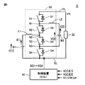
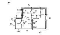
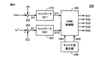
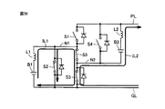
図1は、本発明の実施の形態1に従う電源システムの構成例を示す回路図である。本実施の形態1に従う電源システム5は、特許文献1に示された電源システムと回路構成が共通する。
[Embodiment 1]
(Circuit configuration)
FIG. 1 is a circuit diagram showing a configuration example of a power supply system according to the first embodiment of the present invention. The
図1を参照して、電源システム5は、直流電源B1と、直流電源B2と、負荷30と、制御装置40と、電力変換器50とを備える。
Referring to FIG. 1,
本実施の形態1において、直流電源B1およびB2は、二次電池や電気二重層キャパシタ等の蓄電装置によって構成される。たとえば、直流電源B1は、リチウムイオン二次電池やニッケル水素電池のような二次電池で構成される。また、直流電源B2は、たとえば、電気二重層キャパシタやリチウムイオンキャパシタ等の出力特性に優れた直流電圧源要素により構成される。直流電源B1および直流電源B2は、「第1の直流電源」および「第2の直流電源」にそれぞれ対応する。 In the first embodiment, DC power supplies B1 and B2 are configured by a power storage device such as a secondary battery or an electric double layer capacitor. For example, DC power supply B1 is comprised with secondary batteries, such as a lithium ion secondary battery and a nickel metal hydride battery. The DC power source B2 is constituted by a DC voltage source element having excellent output characteristics such as an electric double layer capacitor and a lithium ion capacitor. The DC power supply B1 and the DC power supply B2 correspond to “first DC power supply” and “second DC power supply”, respectively.
なお、直流電源B1およびB2を同種の蓄電装置によって構成することも可能である。また、直流電源B1およびB2の容量についても特に限定されることはなく、直流電源B1およびB2は、各々を同等の容量で構成してもよく、一方の直流電源の容量を他方の直流電源の容量より大きくしてもよい。 Note that the DC power supplies B1 and B2 can be configured by the same type of power storage device. Further, the capacities of the DC power supplies B1 and B2 are not particularly limited, and each of the DC power supplies B1 and B2 may be configured with an equivalent capacity, and the capacity of one DC power supply may be the same as that of the other DC power supply. It may be larger than the capacity.
電力変換器50は、高電圧側の電力線PLおよび低電圧側の電力線GLの間の直流電圧VH(以下、出力電圧VHとも称する)を制御するように構成される。電力線GLは、代表的には接地配線で構成される。
The
負荷30は、電力変換器50の出力電圧VHを受けて動作する。出力電圧VHの電圧指令値VH*は、負荷30の動作に適した電圧に設定される。電圧指令値VH*は、負荷30の状態に応じて可変に設定されてもよい。さらに、負荷30は、回生発電等によって、直流電源B1および/またはB2の充電電力を発生可能に構成されてもよい。
The
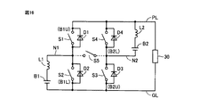
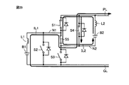
電力変換器50は、電力用半導体スイッチング素子S1〜S4と、リアクトルL1,L2とを含む。本実施の形態1において、電力用半導体スイッチング素子(以下、単に「スイッチング素子」とも称する)としては、IGBT(Insulated Gate Bipolar Transistor)、電力用MOS(Metal Oxide Semiconductor)トランジスタあるいは電力用バイポーラトランジスタ等を用いることができる。スイッチング素子S1〜S4に対しては、逆並列ダイオードD1〜D4が配置されている。スイッチング素子S1〜S4は、制御装置40からの制御信号SG1〜SG4に応答して、オンオフを制御することが可能である。
スイッチング素子S1は、電力線PLおよびノードN1の間に電気的に接続される。リアクトルL2および直流電源B2は、ノードN1とノードN3との間に直列に、電気的に接続される。たとえば、リアクトルL2は、ノードN1と直流電源B2の正極端子との間に電気的に接続されるとともに、直流電源B2の負極端子は、ノードN3と電気的に接続される。なお、リアクトルL2および直流電源B2の接続順序を入れ換えても、電気的に等価な回路構成が形成される。 Switching element S1 is electrically connected between power line PL and node N1. Reactor L2 and DC power supply B2 are electrically connected in series between nodes N1 and N3. For example, reactor L2 is electrically connected between node N1 and the positive terminal of DC power supply B2, and the negative terminal of DC power supply B2 is electrically connected to node N3. Even if the connection order of the reactor L2 and the DC power supply B2 is changed, an electrically equivalent circuit configuration is formed.
スイッチング素子S2は、ノードN1およびN2の間に電気的に接続される。リアクトルL1および直流電源B1は、ノードN2および電力線GLの間に直列に、電気的に接続される。たとえば、リアクトルL1は、直流電源B1の正極端子およびノードN1の間に電気的に接続されるとともに、直流電源B1の負極端子は、電力線GLと電気的に接続される。なお、リアクトルL1および直流電源B1の接続順序を入れ換えても、電気的に等価な回路構成が形成される。 Switching element S2 is electrically connected between nodes N1 and N2. Reactor L1 and DC power supply B1 are electrically connected in series between node N2 and power line GL. For example, reactor L1 is electrically connected between the positive terminal of DC power supply B1 and node N1, and the negative terminal of DC power supply B1 is electrically connected to power line GL. Even if the connection order of the reactor L1 and the DC power supply B1 is changed, an electrically equivalent circuit configuration is formed.
スイッチング素子S3は、ノードN2およびN3の間に電気的に接続される。スイッチング素子S4は、ノードN3および電力線GLの間に電気的に接続される。電力線GLは、負荷30および、直流電源B1の負極端子と電気的に接続される。 Switching element S3 is electrically connected between nodes N2 and N3. Switching element S4 is electrically connected between node N3 and power line GL. Power line GL is electrically connected to load 30 and the negative terminal of DC power supply B1.
図1の構成例では、スイッチング素子S1は「第1のスイッチング素子」に対応し、スイッチング素子S2は「第2のスイッチング素子」に対応し、スイッチング素子S3は「第3のスイッチング素子」に対応し、スイッチング素子S4は「第4のスイッチング素子」に対応する。さらに、リアクトルL1およびL2は、「第1のリアクトル」および「第2のリアクトル」にそれぞれ対応する。 In the configuration example of FIG. 1, the switching element S1 corresponds to a “first switching element”, the switching element S2 corresponds to a “second switching element”, and the switching element S3 corresponds to a “third switching element”. The switching element S4 corresponds to a “fourth switching element”. Furthermore, reactors L1 and L2 correspond to a “first reactor” and a “second reactor”, respectively.
制御装置40は、たとえば、図示しないCPU(Central Processing Unit)およびメモリを有する電子制御ユニット(ECU)によって構成される。制御装置40は、メモリに記憶されたマップおよびプログラムに基づいて、各センサによる検出値を用いた演算処理を行なうように構成される。あるいは、制御装置40の少なくとも一部は、電子回路等のハードウェアにより所定の数値・論理演算処理を実行するように構成されてもよい。
The
制御装置40は、出力電圧VHを制御するために、スイッチング素子S1〜S4のオンオフを制御する制御信号SG1〜SG4を生成する。
The
なお、図1では図示を省略しているが、直流電源B1の電圧(V[1]と表記する)および電流(I[1]と表記する)、直流電源B2の電圧(V[2]と表記する)および電流(I[2]と表記する)、ならびに、出力電圧VHの検出器(電圧センサ,電流センサ)が設けられている。これらの検出器の出力は、制御装置40へ与えられる。
Although not shown in FIG. 1, the voltage (denoted as V [1]) and current (denoted as I [1]) of the DC power supply B1, and the voltage (V [2] of the DC power supply B2). And a detector (voltage sensor, current sensor) for output voltage VH and current (denoted as I [2]) and output voltage VH. The outputs of these detectors are provided to the
実施の形態1に従う電力変換器50は、スイッチング素子S1〜S4の制御によって、直流電源B1,B2が並列に負荷30との間で電力の授受を行なう「パラレル接続モード」と、直列に接続された直流電源B1,B2が負荷30との間で電力の授受を実行する「シリーズ接続モード」とを切替えて動作することが可能である。実施の形態1では、パラレル接続モードにおける制御動作、特に、スイッチング素子による電力損失低減のための制御について説明する。
(パラレル接続モードでの回路動作)
電力変換器50のパラレル接続モードでの制御動作について説明する。
(Circuit operation in parallel connection mode)
A control operation in the parallel connection mode of the
図1を参照して、電力変換器50は、直流電源B1および直流電源B2の各々に対応して昇圧チョッパ回路を備えた構成となっている。すなわち、直流電源B1に対しては、スイッチング素子S1,S2を上アームとする一方で、スイッチング素子S3,S4を下アームとする電流双方向の第1の昇圧チョッパ回路が構成される。
Referring to FIG. 1,
具体的には、第1の昇圧チョッパ回路の下アーム(スイッチング素子S3,S4)は、直流電源B1が力行状態のときにリアクトルL1にエネルギを蓄積するための「第1の電流経路」を形成する一方、直流電源B1が回生状態のときにリアクトルL1の蓄積エネルギを直流電源B1に出力するための「第2の電流経路」を形成する。第1の昇圧チョッパ回路の上アーム(スイッチング素子S1,S2)は、直流電源B1が力行状態のときにリアクトルL1の蓄積エネルギを直流電源B1のエネルギとともに電力線PLに出力するための「第2の電流経路」を形成する一方で、直流電源B1が回生状態のときに電力線PLからの出力をリアクトルL1にエネルギを蓄積するための「第1の電流経路」を形成する。 Specifically, the lower arm (switching elements S3 and S4) of the first step-up chopper circuit forms a “first current path” for storing energy in reactor L1 when DC power supply B1 is in a powering state. On the other hand, when the DC power supply B1 is in the regenerative state, a “second current path” is formed for outputting the stored energy of the reactor L1 to the DC power supply B1. The upper arms (switching elements S1 and S2) of the first step-up chopper circuit “second” for outputting the stored energy of the reactor L1 to the power line PL together with the energy of the DC power supply B1 when the DC power supply B1 is in the power running state. While the “current path” is formed, a “first current path” for storing energy in the reactor L1 from the output from the power line PL when the DC power supply B1 is in the regenerative state is formed.
スイッチング素子S3,S4のペアがオンされる一方で、スイッチング素子S1,S2の少なくとも一方がオフされている第1の期間と、スイッチング素子S1,S2のペアがオンされる一方で、スイッチング素子S3,S4の少なくとも一方がオフされている第2の期間とを交互に繰り返すことにより、第1の電流経路および第2の電流経路が交互に形成される。 While the pair of switching elements S3 and S4 is turned on, the first period in which at least one of the switching elements S1 and S2 is turned off and the pair of switching elements S1 and S2 are turned on, while the switching element S3 , S4 and the second period in which at least one of them is turned off alternately, the first current path and the second current path are alternately formed.
このようなパラレル接続モードにおける直流電源B1に対する直流電力変換において、電圧変換比(昇圧比)は、直流電源B1の電圧V[1]、電力線PLの出力電圧VHおよび直流電源B1の出力デューティ比Da(以下、単にデューティ比Daとも称する)を用いて、下記(1)式で示される。なお、デューティ比は、下アームのオン期間およびオフ期間の和であるスイッチング周期に対する、下アームのオン期間比で定義される。(1)式では、スイッチング素子S3,S4のペアがオンされる第1の期間のデューティ比をDaとする。 In the DC power conversion for the DC power supply B1 in such a parallel connection mode, the voltage conversion ratio (step-up ratio) is the voltage V [1] of the DC power supply B1, the output voltage VH of the power line PL, and the output duty ratio Da of the DC power supply B1. (Hereinafter, also simply referred to as a duty ratio Da) is expressed by the following equation (1). The duty ratio is defined as the ratio of the lower arm on period to the switching period, which is the sum of the lower arm on period and off period. In the equation (1), the duty ratio in the first period when the pair of switching elements S3 and S4 is turned on is Da.
VH=1/(1−Da)・V[1] …(1)
同様に、直流電源B2に対しては、スイッチング素子S1,S4を上アームとする一方で、スイッチング素子S2,S3を下アームとする電流双方向の第2の昇圧チョッパ回路が構成される。第2の昇圧チョッパ回路の下アーム(スイッチング素子S2,S3)は、直流電源B2が力行状態のときにリアクトルL2にエネルギを蓄積するための「第3の電流経路」を形成する一方で、直流電源B2が回生状態のときにリアクトルL2の蓄積エネルギを直流電源B2に出力するための「第4の電流経路」を形成する。第2の昇圧チョッパ回路の上アーム(スイッチング素子S1,S4)は、直流電源B2が力行状態のときにリアクトルL2の蓄積エネルギを直流電源B2のエネルギとともに電力線PLに出力するための「第4の電流経路」を形成する一方で、直流電源B2が回生状態のときに電力線PLからの出力をリアクトルL2にエネルギを蓄積するための「第3の電流経路」を形成する。
VH = 1 / (1-Da) · V [1] (1)
Similarly, for the DC power source B2, a current bidirectional second step-up chopper circuit is configured with the switching elements S1 and S4 as upper arms and the switching elements S2 and S3 as lower arms. The lower arms (switching elements S2, S3) of the second boost chopper circuit form a “third current path” for storing energy in the reactor L2 when the DC power supply B2 is in a power running state, A “fourth current path” is formed for outputting the energy stored in reactor L2 to DC power supply B2 when power supply B2 is in the regenerative state. The upper arm (switching elements S1 and S4) of the second boost chopper circuit outputs “the fourth energy stored in reactor L2 together with the energy of DC power supply B2 to power line PL when DC power supply B2 is in a powering state. While the “current path” is formed, a “third current path” is formed for accumulating the energy from the output from the power line PL in the reactor L2 when the DC power supply B2 is in the regenerative state.
スイッチング素子S2,S3のペアがオンされる一方で、スイッチング素子S1,S4の少なくとも一方がオフされている第1の期間と、スイッチング素子S1,S4のペアがオンされる一方で、スイッチング素子S2,S3の少なくとも一方がオフされている第2の期間とを交互に繰り返すことにより、第3の電流経路および第4の電流経路が交互に形成される。 While the pair of switching elements S2 and S3 is turned on, the first period when at least one of the switching elements S1 and S4 is turned off, and the pair of switching elements S1 and S4 is turned on, while the switching element S2 , S3 and the second period in which at least one of them is turned off alternately, the third current path and the fourth current path are alternately formed.
このようなパラレル接続モードにおける直流電源B2に対する直流電力変換において、電圧変換比(昇圧比)は、直流電源B2の電圧V[2]、電力線PLの出力電圧VHおよび直流電源B2からの出力デューティ比Db(以下、単にデューティ比Dbとも称する)を用いて、下記(2)式で示される。(2)式では、スイッチング素子S2,S3のペアがオンされる第1の期間のデューティ比をDbとする。 In the DC power conversion for the DC power supply B2 in such a parallel connection mode, the voltage conversion ratio (step-up ratio) is the voltage V [2] of the DC power supply B2, the output voltage VH of the power line PL, and the output duty ratio from the DC power supply B2. Using Db (hereinafter, also simply referred to as duty ratio Db), the following equation (2) is used. In the equation (2), Db is a duty ratio in a first period in which the pair of switching elements S2 and S3 is turned on.
VH=1/(1−Db)・V[2] …(2)
なお、図1から理解されるように、スイッチング素子S1〜S4の各々は、第1の昇圧チョッパ回路によって直流電源B1および電力線PLの間に形成される第1および第2の電流経路のいずれか一方と、第2の昇圧チョッパ回路によって直流電源B2および電力線PLの間に形成される第3および第4の電流経路のいずれか一方との両方に含まれるように配置されている。
VH = 1 / (1-Db) · V [2] (2)
As can be understood from FIG. 1, each of the switching elements S1 to S4 is one of the first and second current paths formed between the DC power supply B1 and the power line PL by the first boost chopper circuit. One of them is arranged so as to be included in both one of the third and fourth current paths formed between DC power supply B2 and power line PL by the second boost chopper circuit.
(パラレル接続モードでの制御動作)
電力変換器50でのパラレル接続モードにおける制御動作について説明する。以下に説明する制御動作は、制御装置40によるハードウェア処理および/またはソフトウェア処理によって実現される。
(Control operation in parallel connection mode)
A control operation in the parallel connection mode in the
電力変換器50をパラレル接続モードで動作させる場合には、直流電源B1および直流電源B2のそれぞれについてパルス幅変調(PWM)制御が並列に実行される。パラレル接続モードでは、特許文献1に記載のパラレル接続モードと同様に、直流電源B1およびB2の一方の出力を、出力電圧VHの電圧偏差ΔV(ΔV=VH*−VH)を補償するように制御(電圧制御)するとともに、直流電源B1およびB2の他方の出力を、電流I[1]またはI[2]の電流偏差を補償するように制御(電流制御)することができる。たとえば、電流制御の指令値(Io*)は、当該電源の出力電力を制御するように設定することができる。
When
一例として、直流電源B1のデューティ比Daは、直流電源B1が電圧源として動作するための電圧フィードバック制御または電流源として動作するための電流フィードバック制御によって算出される。直流電源B2のデューティ比Dbは、直流電源B1が電圧源として動作するときには、直流電源B2が電流源として動作するための電流フィードバック制御によって算出される。反対に、デューティ比Dbは、直流電源B1が電流源として動作するときには、直流電源B2が電圧源として動作するための電圧フィードバック制御によって算出される。 As an example, the duty ratio Da of the DC power supply B1 is calculated by voltage feedback control for operating the DC power supply B1 as a voltage source or current feedback control for operating as a current source. The duty ratio Db of the DC power supply B2 is calculated by current feedback control for operating the DC power supply B2 as a current source when the DC power supply B1 operates as a voltage source. On the contrary, the duty ratio Db is calculated by voltage feedback control for operating the DC power supply B2 as a voltage source when the DC power supply B1 operates as a current source.
(パラレル接続モードでのスイッチング損失低減のための制御動作)
電力変換器50のパラレル接続モードにおける基本的な制御動作は、特許文献1のパラレル接続モードでの制御動作と同等であるため、これに対する詳細な説明は省略する。ここでは、直流電源B1および直流電源B2のPWM制御に使用されるキャリア波の位相制御(以下、「キャリア位相制御」とも称する)について説明する。
(Control operation to reduce switching loss in parallel connection mode)
Since the basic control operation in the parallel connection mode of the
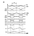
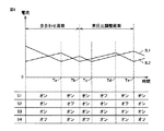
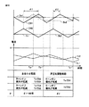
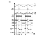
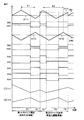
(1)キャリア位相制御
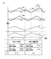
図2は、位相が異なるキャリア波を用いた場合におけるパラレル制御モードの制御動作例が示す波形図である。
(1) Carrier Phase Control FIG. 2 is a waveform diagram showing a control operation example in the parallel control mode when carrier waves having different phases are used.
図2を参照して、直流電源B1のPWM制御に用いられるキャリア波CW1と、直流電源B2のPWM制御に用いられるキャリア波CW2とは、同一周波数であるが位相が異なる。図2の例では、キャリア波CW1およびCW2間の位相差φ=180度である。キャリア波CW1,CW2には、三角波が用いられる。キャリア波CW1,CW2の周期は、各スイッチング素子のスイッチング周波数に相当する。キャリア波CW1の振幅はデューティ比Da=1.0に対応する電圧に設定される。キャリア波CW2の振幅はデューティ比Db=1.0に対応する電圧に設定される。 Referring to FIG. 2, carrier wave CW1 used for PWM control of DC power supply B1 and carrier wave CW2 used for PWM control of DC power supply B2 have the same frequency but different phases. In the example of FIG. 2, the phase difference between carrier waves CW1 and CW2 is φ = 180 degrees. Triangular waves are used for the carrier waves CW1 and CW2. The period of carrier waves CW1 and CW2 corresponds to the switching frequency of each switching element. The amplitude of the carrier wave CW1 is set to a voltage corresponding to the duty ratio Da = 1.0. The amplitude of carrier wave CW2 is set to a voltage corresponding to duty ratio Db = 1.0.
直流電源B1の出力を制御(電圧または電流制御)するためのデューティ比Daと、キャリア波CW1との電圧比較に基づいて、制御パルス信号SDaが生成される。制御パルス信号SDaは、デューティ比Daを示す電圧が、キャリア波CW1の電圧よりも高いときに論理ハイレベル(以下、Hレベル)に設定される一方で、キャリア波CW1の電圧よりも低いときに論理ローレベル(以下、Lレベル)に設定される。制御パルス信号SDaの周期(Hレベル期間+Lレベル期間)に対するHレベル期間の比、すなわち、制御パルス信号SDaのデューティ比は、Daと同等である。 A control pulse signal SDa is generated based on a voltage comparison between the duty ratio Da for controlling (voltage or current control) the output of the DC power supply B1 and the carrier wave CW1. Control pulse signal SDa is set to a logic high level (hereinafter referred to as H level) when the voltage indicating duty ratio Da is higher than the voltage of carrier wave CW1, while it is lower than the voltage of carrier wave CW1. It is set to a logic low level (hereinafter referred to as L level). The ratio of the H level period to the cycle (H level period + L level period) of the control pulse signal SDa, that is, the duty ratio of the control pulse signal SDa is equal to Da.
制御パルス信号/SDaは、制御パルス信号SDaの反転信号である。デューティ比Daが高くなると、制御パルス信号SDaのHレベル期間が長くなる。反対に、デューティ比Daが低くなると、制御パルス信号SDaのLレベル期間が長くなる。 Control pulse signal / SDa is an inverted signal of control pulse signal SDa. As the duty ratio Da increases, the H level period of the control pulse signal SDa increases. On the other hand, when the duty ratio Da decreases, the L level period of the control pulse signal SDa increases.
制御パルス信号SDaは、上述した第1の昇圧チョッパ回路の下アーム(スイッチング素子S3,S4)のオンオフを制御する信号に対応する。一方、制御パルス信号/SDaは、第1の昇圧チョッパ回路の上アーム(スイッチング素子S1,S2)のオンオフを制御する信号に対応する。 The control pulse signal SDa corresponds to a signal for controlling on / off of the lower arms (switching elements S3 and S4) of the first boost chopper circuit described above. On the other hand, the control pulse signal / SDa corresponds to a signal for controlling on / off of the upper arms (switching elements S1, S2) of the first boost chopper circuit.
同様に、直流電源B2の出力を制御(電流または電圧制御)するためのデューティ比Dbと、キャリア波CW2との電圧比較に基づいて、制御パルス信号SDbおよび、その反転信号/SDbが生成される。制御パルス信号SDbのデューティ比はDbと同様であり、制御パルス信号/SDbのデューティ比は(1.0−Db)と同等である。すなわち、デューティ比Dbが高くなると、制御パルス信号SDbのHレベル期間が長くなる。反対に、デューティ比Dbが低くなると、制御パルス信号SDbのLレベル期間が長くなる。 Similarly, control pulse signal SDb and its inverted signal / SDb are generated based on voltage comparison between duty ratio Db for controlling output (current or voltage control) of DC power supply B2 and carrier wave CW2. . The duty ratio of control pulse signal SDb is the same as Db, and the duty ratio of control pulse signal / SDb is equivalent to (1.0−Db). That is, as the duty ratio Db increases, the H level period of the control pulse signal SDb increases. On the contrary, when the duty ratio Db decreases, the L level period of the control pulse signal SDb increases.
制御パルス信号SDbは、上述した第2の昇圧チョッパ回路の下アーム(スイッチング素子S2,S3)のオンオフを制御する信号に対応する。一方、制御パルス信号/SDbは、第2の昇圧チョッパ回路の上アーム(スイッチング素子S1,S4)のオンオフを制御する信号に対応する。 The control pulse signal SDb corresponds to a signal for controlling on / off of the lower arms (switching elements S2, S3) of the second boost chopper circuit described above. On the other hand, control pulse signal / SDb corresponds to a signal for controlling on / off of the upper arm (switching elements S1, S4) of the second boost chopper circuit.
制御信号SG1〜SG4は、制御パルス信号SDa(/SDa)およびSDb(/SDb)の論理演算に基づいて設定される。制御信号SG1〜SG4に基づいてスイッチング素子S1〜S4をオンオフすることにより、リアクトルL1を流れるリアクトル電流IL1の増減、およびリアクトルL2を流れるリアクトル電流IL2の増減が図2に示すように制御される。リアクトル電流IL1は直流電源B1の電流I[1]に相当し、リアクトル電流IL2は直流電源B2の電流I[2]に相当する。 Control signals SG1 to SG4 are set based on a logical operation of control pulse signals SDa (/ SDa) and SDb (/ SDb). By turning on and off switching elements S1 to S4 based on control signals SG1 to SG4, increase / decrease in reactor current IL1 flowing through reactor L1 and increase / decrease in reactor current IL2 flowing through reactor L2 are controlled as shown in FIG. Reactor current IL1 corresponds to current I [1] of DC power supply B1, and reactor current IL2 corresponds to current I [2] of DC power supply B2.
図2に示されるように、キャリア波CW1とキャリア波CW2との間に位相差φを設けることにより、制御パルス信号SDaは、位相差φ=0のときの制御パルス信号SDaと比較して、Hレベル期間の長さは同じであるものの位相が異なる。同様に、制御パルス信号SDbは、位相差φ=0のときの制御パルス信号SDbと比較して、Hレベル期間の長さが同じであるものの位相が異なる。その結果、制御信号SG1〜SG4は、位相差φ=0のときの制御信号SG1〜SG4とは異なった波形となる。よって、キャリア波CW1およびCW2の間の位相差φを変化させることにより、リアクトル電流IL1およびリアクトル電流IL2の位相関係(電流位相)も変化することが理解される。 As shown in FIG. 2, by providing a phase difference φ between the carrier wave CW1 and the carrier wave CW2, the control pulse signal SDa is compared with the control pulse signal SDa when the phase difference φ = 0. Although the length of the H level period is the same, the phase is different. Similarly, control pulse signal SDb has the same H-level period length but a different phase compared to control pulse signal SDb when phase difference φ = 0. As a result, the control signals SG1 to SG4 have different waveforms from the control signals SG1 to SG4 when the phase difference φ = 0. Therefore, it is understood that the phase relationship (current phase) between reactor current IL1 and reactor current IL2 also changes by changing phase difference φ between carrier waves CW1 and CW2.
一方で、同一のデューティ比Da,Dbに対して、リアクトル電流IL1,IL2の平均値は、位相差φを変化させても変化しないことが理解される。すなわち、直流電源B1,B2の出力は、デューティ比Da,Dbによって制御されるものであり、キャリア波CW1,CW2間の位相差φを変化させても影響が生じない。 On the other hand, with respect to the same duty ratio Da, Db, it is understood that the average value of reactor currents IL1, IL2 does not change even when phase difference φ is changed. That is, the outputs of the DC power supplies B1 and B2 are controlled by the duty ratios Da and Db, and there is no effect even if the phase difference φ between the carrier waves CW1 and CW2 is changed.
したがって、キャリア波CW1,CW2間の位相差φを適切に調整するキャリア位相制御によって、電力変換器50のパラレル接続モードにおける、スイッチング素子S1〜S4の電力損失を低減することができる。
Therefore, the power loss of switching elements S1 to S4 in the parallel connection mode of
以下では、代表的な例として、直流電源B1およびB2の両方が力行状態、すなわちリアクトル電流IL1>0かつリアクトル電流IL2>0である状態での制御について説明する。 In the following, as a representative example, control in a state where both DC power sources B1 and B2 are in a power running state, that is, a reactor current IL1> 0 and a reactor current IL2> 0 will be described.
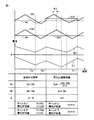
図3は、パラレル接続モードにおけるキャリア位相制御の動作例を説明するための波形図である。 FIG. 3 is a waveform diagram for explaining an operation example of carrier phase control in the parallel connection mode.
図3を参照して、時刻Taまでは、スイッチング素子S2〜S4がオンされるので、直流電源B1,B2の両方に対して、昇圧チョッパ回路の下アーム(第1および第3の電流経路)がオンされた状態となる。このため、リアクトル電流IL1およびIL2の両方は上昇する。 Referring to FIG. 3, switching elements S2 to S4 are turned on until time Ta, so that the lower arm (first and third current paths) of the boost chopper circuit with respect to both DC power supplies B1 and B2. Is turned on. For this reason, both reactor currents IL1 and IL2 rise.
時刻Taにおいて、スイッチング素子S2がターンオフされることにより、直流電源B2に対して昇圧チョッパ回路の下アーム(第3の電流経路)がオフされた状態となるので、リアクトル電流IL2が上昇から下降に転じる。すなわち、リアクトル電流IL2は極大となる。スイッチング素子S2のターンオフと入替わりに、スイッチング素子S1がターンオンされる。 At time Ta, the switching element S2 is turned off, so that the lower arm (third current path) of the step-up chopper circuit is turned off with respect to the DC power supply B2, so that the reactor current IL2 decreases from rising to falling. Turn. That is, reactor current IL2 becomes maximum. Instead of switching off the switching element S2, the switching element S1 is turned on.
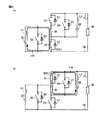
時刻Ta以降では、直流電源B1に対して昇圧チョッパ回路の下アーム(第1の電流経路)がオンされ、直流電源B2に対して昇圧チョッパ回路の下アームがオフされた状態となる。すなわち、リアクトル電流IL2が上昇する一方で、リアクトル電流IL1が下降する。このとき、電力変換器50での電流経路は、図4(a)のようになる。
After the time Ta, the lower arm (first current path) of the boost chopper circuit is turned on with respect to the DC power supply B1, and the lower arm of the boost chopper circuit is turned off with respect to the DC power supply B2. That is, reactor current IL2 rises, while reactor current IL1 falls. At this time, the current path in the
図4(a)から理解されるように、時刻Ta以降では、スイッチング素子S4には、リアクトル電流IL1およびIL2の差電流が通過することになる。すなわち、スイッチング素子S4の通過電流が小さくなる。 As understood from FIG. 4A, after the time Ta, the difference current between the reactor currents IL1 and IL2 passes through the switching element S4. That is, the passing current of the switching element S4 becomes small.
再び図3を参照して、時刻Tb以降の状態から、スイッチング素子S4がターンオフすると、直流電源B1に対して昇圧チョッパ回路の下アームがオフされた状態となるので、リアクトル電流IL1が上昇から下降に転じる。すなわち、リアクトル電流IL1は極大となる。また、スイッチング素子S2がターンオンすると、直流電源B2に対して昇圧チョッパ回路の下アームがオンされた状態となるので、リアクトル電流IL2が再び下降から上昇に転じる。すなわち、リアクトル電流IL2は極小となる。これにより、電力変換器50での電流経路が、図4(a)の状態から、図4(b)の状態に変化する。図4(b)の状態では、スイッチング素子S2には、リアクトル電流IL1およびIL2の差電流が通過することになるため、スイッチング素子S2の通過電流が小さくなる。
Referring to FIG. 3 again, when switching element S4 is turned off from the state after time Tb, the lower arm of step-up chopper circuit is turned off with respect to DC power supply B1, so that reactor current IL1 falls from the rise. Turn to. That is, reactor current IL1 becomes maximum. Further, when switching element S2 is turned on, the lower arm of the step-up chopper circuit is turned on with respect to DC power supply B2, so that reactor current IL2 changes from falling to rising again. That is, reactor current IL2 is minimal. As a result, the current path in the
図4(a)の状態でスイッチング素子S4をターンオフさせることにより、スイッチング素子S4のターンオフ時の電流が低減してソフトスイッチングとなり、スイッチング損失を低減できる。また、図4(b)の状態でスイッチング素子S2をターンオンさせることにより、スイッチング素子S2のターンオン時の電流が低減してソフトスイッチングとなり、スイッチング損失を低減できる。 When the switching element S4 is turned off in the state of FIG. 4A, the current when the switching element S4 is turned off is reduced to perform soft switching, and the switching loss can be reduced. Further, by turning on the switching element S2 in the state of FIG. 4B, the current when the switching element S2 is turned on is reduced to perform soft switching, and the switching loss can be reduced.
したがって、図3に示されるように、リアクトル電流IL1が上昇から下降に転じるタイミングと、リアクトル電流IL2が下降から上昇に転じるタイミングとが重なるように、電流位相、すなわち、キャリア波CW1,CW2の位相差φを調整する。すなわち、リアクトル電流IL1の変曲点(極大点)と、リアクトル電流IL2の変曲点(極小点)とが同一タイミングとなるように位相差φを調整する。これにより、図3の時刻Tbにおいて、スイッチング素子S2がターンオンされるとともに、スイッチング素子S4がターンオフされる。 Therefore, as shown in FIG. 3, the current phase, that is, the level of the carrier waves CW1 and CW2, is such that the timing at which the reactor current IL1 changes from rising to falling overlaps the timing at which the reactor current IL2 changes from falling to rising. Adjust the phase difference φ. That is, the phase difference φ is adjusted so that the inflection point (maximum point) of reactor current IL1 and the inflection point (minimum point) of reactor current IL2 are at the same timing. Thereby, at time Tb in FIG. 3, the switching element S2 is turned on and the switching element S4 is turned off.
再び図3を参照して、時刻Tcでは、スイッチング素子S1がターンオフされるとともに、スイッチング素子S4がターンオンされる。これにより、直流電源B1に対して昇圧チョッパ回路の下アームがオフされた状態となるので、リアクトル電流IL1が下降から上昇に転じる。すなわち、リアクトル電流IL2は極小となる。スイッチング素子S2のターンオフと入替わりに、スイッチング素子S1がターンオンされることにより、直流電源B1,B2の各々に対して昇圧チョッパ回路の下アームがオンされた状態となる。したがって、上述した時刻Ta以前の状態が再現されて、リアクトル電流IL1およびIL2の両方が上昇する。 Referring to FIG. 3 again, at time Tc, switching element S1 is turned off and switching element S4 is turned on. As a result, the lower arm of the step-up chopper circuit is turned off with respect to the DC power source B1, and the reactor current IL1 changes from falling to rising. That is, reactor current IL2 is minimal. When the switching element S1 is turned on instead of turning off the switching element S2, the lower arm of the step-up chopper circuit is turned on for each of the DC power supplies B1 and B2. Therefore, the state before time Ta described above is reproduced, and both reactor currents IL1 and IL2 rise.
このように、直流電源B1およびB2の両方が力行状態であるときには、リアクトル電流IL1の極大点と、リアクトル電流IL2の極小点とが図中の時刻Tbで重なるような電流位相となるように、キャリア波CW1,CW2間の位相差φを調整する。これにより、時刻Tbにおけるスイッチング素子S2のターンオン損失およびスイッチング素子S4のターンオフ損失を低減できる。 Thus, when both DC power supplies B1 and B2 are in a power running state, the current phase is such that the maximum point of reactor current IL1 and the minimum point of reactor current IL2 overlap at time Tb in the figure. The phase difference φ between the carrier waves CW1 and CW2 is adjusted. Thereby, the turn-on loss of switching element S2 and the turn-off loss of switching element S4 at time Tb can be reduced.
しかしながら、図3から理解されるように、位相差φを調整することでリアクトル電流IL1の変曲点(極大点または極小点)とリアクトル電流IL2の変曲点(極大点または極小点)とが一致するタイミングは、キャリア波CW1,CW2の1周期(以下、1キャリア周期とも称する)において1回のみである。言い換えれば、キャリア位相制御によってスイッチング損失を低減することができるタイミングは、1キャリア周期において1回のみである。 However, as understood from FIG. 3, the inflection point (maximum point or minimum point) of reactor current IL1 and the inflection point (maximum point or minimum point) of reactor current IL2 are adjusted by adjusting phase difference φ. The coincidence timing is only once in one period (hereinafter also referred to as one carrier period) of the carrier waves CW1 and CW2. In other words, the timing at which switching loss can be reduced by carrier phase control is only once in one carrier period.
そのため、リアクトル電流IL2が極大となるタイミングである時刻Taでは、スイッチング素子S2のターンオフ時の電流が大きくハードスイッチングとなるため、スイッチング素子S2のターンオフ損失が増加することが懸念される。同様に、リアクトル電流IL1が極小となるタイミングである時刻Tcでは、スイッチング素子S4のターンオン時の電流が大きくハードスイッチングとなるため、スイッチング素子S4のターンオン損失が増加することが懸念される。 Therefore, at time Ta, which is the timing when the reactor current IL2 becomes maximum, the current at the time of turn-off of the switching element S2 is large and hard switching is performed, so there is a concern that the turn-off loss of the switching element S2 increases. Similarly, at the time Tc when the reactor current IL1 is minimized, the current at the turn-on of the switching element S4 is large and hard switching is performed, so there is a concern that the turn-on loss of the switching element S4 increases.
これに対して、実施の形態1に従う電力変換器50のパラレル接続モードでは、以下に説明するように、キャリア位相制御に並行して、直流電源B1のデューティ比Daおよび直流電源B2のデューティ比Dbを適切に調整する制御(以下、「デューティ比制御」とも称する)を行なうことにより、スイッチング素子S1〜S4のスイッチング損失のさらなる低減を図る。
In contrast, in the parallel connection mode of
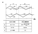
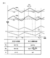
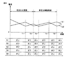
(2)デューティ比制御
図5は、実施の形態1に従う電力変換器50に対するデューティ比制御の適用を説明するための波形図である。
(2) Duty Ratio Control FIG. 5 is a waveform diagram for explaining the application of duty ratio control to
図5を参照して、デューティ比制御の適用時には、デューティ比Da,Dbを調整することにより、制御パルス信号SDaのHレベル期間(=制御パルス信号/SDaのLレベル期間)および制御パルス信号SDbのHレベル期間(=制御パルス信号/SDbのLレベル期間)を調整する。 Referring to FIG. 5, when duty ratio control is applied, by adjusting duty ratios Da and Db, H level period of control pulse signal SDa (= control pulse signal / L level period of SDa) and control pulse signal SDb H level period (= control pulse signal / L level period of SDb) is adjusted.
上述のように、キャリア位相制御は、キャリア波CW1,CW2間の位相差φを変化させることによって、リアクトル電流IL1およびリアクトル電流IL2の位相関係(電流位相)を変化させるものである。これに対して、デューティ比制御は、デューティ比Da,Dbを変化させることによって、リアクトル電流IL1,IL2の波形を変化させるものである。実施の形態1では、キャリア位相制御とデューティ比制御とを組み合わせることで、1キャリア周期におけるリアクトル電流IL1の変曲点とリアクトル電流IL2の変曲点とが一致するタイミングを増やすことができる。 As described above, the carrier phase control changes the phase relationship (current phase) between the reactor current IL1 and the reactor current IL2 by changing the phase difference φ between the carrier waves CW1 and CW2. On the other hand, in the duty ratio control, the waveforms of the reactor currents IL1 and IL2 are changed by changing the duty ratios Da and Db. In the first embodiment, by combining carrier phase control and duty ratio control, the timing at which the inflection point of reactor current IL1 and the inflection point of reactor current IL2 coincide with each other in one carrier cycle can be increased.
その一方で、デューティ比Da,Dbを変化させると、直流電源B1,B2の出力も変化する。その結果、直流電源B1およびB2間の電力配分が変化してしまい、出力電圧VHを電圧指令値VH*に制御することが困難となる。 On the other hand, when the duty ratios Da and Db are changed, the outputs of the DC power supplies B1 and B2 are also changed. As a result, the power distribution between the DC power supplies B1 and B2 changes, and it becomes difficult to control the output voltage VH to the voltage command value VH *.
したがって、実施の形態1に従う電力変換器50では、複数のキャリア周期を「1調整期間」として、当該1調整期間を通算したデューティ比Daの平均値が、直流電源B1の出力を制御(電圧/電流制御)するためのデューティ比に相当するとともに、1調整期間を通算したデューティ比Dbの平均値が、直流電源B2の出力を制御(電流/電圧制御)するためのデューティ比に相当するように、各キャリア周期におけるデューティ比Da,Dbを調整する。すなわち、1調整期間単位で、直流電源B1,B2の出力制御のためのデューティ比を保障する。これにより、各キャリア周期におけるデューティ比Da,Dbを変化させても直流電源B1およびB2間の電力配分に影響を生じさせないようにする。
Therefore, in
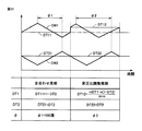
具体的には、m個(mは2以上の整数)のキャリア周期を1調整期間とし、当該1調整期間を、n個(nは1以上m未満の整数)の「第1のキャリア周期」と、(m−n)個の「第2のキャリア周期」とから構成する。図5では、説明の簡素化のため、m=2とし、かつ、n=1としたときの電力変換器50の動作例を示している。すなわち、図5は、第1のキャリア周期と第2のキャリア周期とが交互に形成される例を示している。
Specifically, m carrier cycles (m is an integer equal to or greater than 2) are defined as one adjustment period, and n (n is an integer equal to or greater than 1 and less than m) “first carrier cycle”. And (mn) “second carrier periods”. FIG. 5 shows an operation example of the
第1のキャリア周期では、リアクトル電流IL1の2つの変曲点(極大点および極小点)と、リアクトル電流IL2の2つの変曲点とがそれぞれ同一タイミングとなるように、デューティ比Da,Dbを調整するとともに、位相差φを調整する。図5では、第1のキャリア周期における直流電源B1のデューティ比をDa1とし、直流電源B2のデューティ比をDb1とする。また、第1のキャリア周期における位相差をφ1とする。 In the first carrier cycle, the duty ratios Da and Db are set so that the two inflection points (maximum point and minimum point) of the reactor current IL1 and the two inflection points of the reactor current IL2 have the same timing. While adjusting, the phase difference φ is adjusted. In FIG. 5, the duty ratio of the DC power supply B1 in the first carrier cycle is Da1, and the duty ratio of the DC power supply B2 is Db1. Further, the phase difference in the first carrier period is φ1.
一方、第2のキャリア周期では、第1のキャリア周期におけるデューティ比Da1,Db2に基づいて、デューティ比Da,Dbを調整する。具体的には、1調整期間を通算したデューティ比Da,Dbの平均値がそれぞれ、直流電源B1,B2の出力制御によって算出されるデューティ比に相当するように、第1のキャリア周期におけるデューティ比Da1,Db2に基づいて、デューティ比Da,Dbを調整する。図5では、第2のキャリア周期における直流電源B1のデューティ比をDa2とし、直流電源B2のデューティ比をDb2とする。さらに、リアクトル電流IL1の2つの変曲点の一方(極大点)と、リアクトル電流IL2の2つの変曲点の一方(極小点)とが同一タイミングとなるように、調整されたデューティ比Da2,Db2に応じて位相差φを調整する。第2のキャリア周期における位相差をφ2とする。 On the other hand, in the second carrier period, the duty ratios Da and Db are adjusted based on the duty ratios Da1 and Db2 in the first carrier period. Specifically, the duty ratio in the first carrier cycle is such that the average values of the duty ratios Da and Db for one adjustment period correspond to the duty ratio calculated by the output control of the DC power supplies B1 and B2, respectively. The duty ratios Da and Db are adjusted based on Da1 and Db2. In FIG. 5, the duty ratio of the DC power supply B1 in the second carrier cycle is Da2, and the duty ratio of the DC power supply B2 is Db2. Further, the duty ratio Da2, adjusted so that one of the two inflection points (maximum point) of the reactor current IL1 and one of the two inflection points (minimum point) of the reactor current IL2 are at the same timing. The phase difference φ is adjusted according to Db2. The phase difference in the second carrier period is φ2.
すなわち、第1のキャリア周期は、リアクトル電流IL1,IL2の2つの変曲点のタイミングを一致させることに特化した制御が行なわれる周期(以下、「全合わせ周期」とも称する)に相当する。これに対して、第2のキャリア周期は、1調整期間単位で直流電源B1,B2の出力制御のためのデューティ比を保障するための制御が行なわれる周期(以下、「昇圧比調整周期」とも称する)に相当する。なお、昇圧比調整周期においても、リアクトル電流IL1,IL2の変曲点を同一タイミングとするための位相差φの調整が行なわれる。 That is, the first carrier period corresponds to a period (hereinafter, also referred to as “total alignment period”) in which control specialized in matching the timings of the two inflection points of reactor currents IL1 and IL2 is performed. On the other hand, the second carrier cycle is a cycle in which control for ensuring the duty ratio for output control of the DC power supplies B1 and B2 is performed in units of one adjustment period (hereinafter referred to as “step-up ratio adjustment cycle”). It corresponds to). Also in the step-up ratio adjustment cycle, the phase difference φ is adjusted so that the inflection points of reactor currents IL1 and IL2 have the same timing.
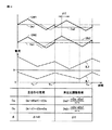
次に、第1のキャリア周期および第2のキャリア周期における電力変換器50の動作および制御について詳細に説明する。以下では、代表的な例として、直流電源B1およびB2の両方が力行状態、すなわちリアクトル電流IL1>0かつリアクトル電流IL2>0である状態での制御について説明する。
Next, the operation and control of
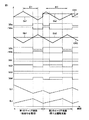
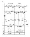
図6は、電力変換器50においてパラレル接続モードにおけるスイッチング損失を低減するための、実施の形態1によるデューティ比制御およびキャリア位相制御による電流位相を説明する波形図である。
FIG. 6 is a waveform diagram illustrating the current phase by duty ratio control and carrier phase control according to the first embodiment for reducing switching loss in the parallel connection mode in
(2−1)第1のキャリア周期における制御動作
図6を参照して、時刻Taまでは、スイッチング素子S1,S2がオンされるので、直流電源B1に対して昇圧チョッパ回路の上アーム(第2の電流経路)がオンされた状態となる。このため、リアクトル電流IL1は下降する。また、スイッチング素子S2,S3がオンされるので、直流電源B2に対しては昇圧チョッパ回路の下アーム(第3の電流経路)がオンされた状態となる。このため、リアクトル電流IL2は上昇する。すなわち、リアクトル電流IL1が下降する一方で、リアクトル電流IL2が上昇する。このとき、電力変換器50での電流経路は、図4(b)のようになる。図4(b)の状態では、スイッチング素子S2には、リアクトル電流IL1およびIL2の差電流が通過することになるため、スイッチング素子S2の通過電流が小さくなる。
(2-1) Control Operation in First Carrier Cycle Referring to FIG. 6, switching elements S1 and S2 are turned on until time Ta, so that the upper arm (the first step of the boost chopper circuit with respect to DC power supply B1) 2 current path) is turned on. For this reason, reactor current IL1 falls. Further, since the switching elements S2 and S3 are turned on, the lower arm (third current path) of the boost chopper circuit is turned on with respect to the DC power supply B2. For this reason, reactor current IL2 rises. That is, reactor current IL1 decreases while reactor current IL2 increases. At this time, the current path in the
時刻Taにおいて、スイッチング素子S4がターンオンされることにより、直流電源B1に対して昇圧チョッパ回路の下アーム(第1の電流経路)がオンされた状態となるので、リアクトル電流IL1が上昇を開始する。また、スイッチング素子S2がターンオフすると、直流電源B2に対して昇圧チョッパ回路の上アーム(第4の電流経路)がオフされた状態となるので、リアクトル電流IL2が下降を開始する。すなわち、電力変換器50での電流経路が、図4(b)の状態から、図4(a)の状態に変化する。図4(a)の状態では、スイッチング素子S4には、リアクトル電流IL1およびIL2の差電流が通過することになるため、スイッチング素子S4の通過電流が小さくなる。
At time Ta, switching element S4 is turned on, so that lower arm (first current path) of boost chopper circuit is turned on with respect to DC power supply B1, and reactor current IL1 starts to rise. . When switching element S2 is turned off, the upper arm (fourth current path) of the step-up chopper circuit is turned off with respect to DC power supply B2, so that reactor current IL2 starts to fall. That is, the current path in the
図4(b)の状態でスイッチング素子S2をターンオフさせることにより、スイッチング素子S2のターンオフ時の電流、すなわち、ターンオフ損失を低減できる。また、図4(a)の状態でスイッチング素子S4をターンオンさせることにより、スイッチング素子S4のターンオン時の電流、すなわち、ターンオン損失を低減できる。 By turning off the switching element S2 in the state of FIG. 4B, the current at the time of turning off the switching element S2, that is, the turn-off loss can be reduced. Further, by turning on the switching element S4 in the state of FIG. 4A, it is possible to reduce the current when the switching element S4 is turned on, that is, the turn-on loss.
したがって、図6に示されるように、リアクトル電流IL1の上昇タイミングと、リアクトル電流IL2の下降タイミングとが重なるように、デューティ比Da1,Db1を調整するとともに位相差φ1を調整する。これにより、時刻Taにおいて、スイッチング素子S2がターンオフされるとともに、スイッチング素子S4がターンオンされる。なお、リアクトル電流IL1の上昇タイミングは、第2の電流経路から第1の電流経路へ切換えるときのリアクトル電流IL1の変曲点に相当し、リアクトル電流IL2の下降タイミングは、第3の電流経路から第4の電流経路へ切換えるときのリアクトル電流IL2の変曲点に相当する。 Therefore, as shown in FIG. 6, the duty ratios Da1 and Db1 are adjusted and the phase difference φ1 is adjusted so that the rising timing of the reactor current IL1 and the falling timing of the reactor current IL2 overlap. Thereby, at time Ta, switching element S2 is turned off and switching element S4 is turned on. The rising timing of reactor current IL1 corresponds to the inflection point of reactor current IL1 when switching from the second current path to the first current path, and the falling timing of reactor current IL2 is from the third current path. This corresponds to the inflection point of the reactor current IL2 when switching to the fourth current path.
さらに、実施の形態1では、図3の時刻Tbと同様に、時刻Tbにおいて、スイッチング素子S2がターンオンされるとともに、スイッチング素子S4がターンオフされる。これにより、リアクトル電流IL1が再び下降を開始するとともに、リアクトル電流IL2が再び上昇を開始する。すなわち、電力変換器50での電流経路が、図4(a)の状態から、図4(b)の状態に変化する。リアクトル電流IL1の下降タイミングと、リアクトル電流IL2の上昇タイミングとが時刻Tbで一致することによって、時刻Tbにおけるスイッチング素子S2のターンオン損失およびスイッチング素子S4のターンオフ損失を低減できる。なお、リアクトル電流IL1の下降タイミングは、第1の電流経路から第2の電流経路へ切換えるときのリアクトル電流IL1の変曲点に相当し、リアクトル電流IL2の上昇タイミングは、第4の電流経路から第3の電流経路へ切換えるときのリアクトル電流IL2の変曲点に相当する。
Further, in the first embodiment, switching element S2 is turned on and switching element S4 is turned off at time Tb, similarly to time Tb in FIG. Thereby, reactor current IL1 starts to fall again, and reactor current IL2 starts to rise again. That is, the current path in the
このように、第1のキャリア周期では、デューティ比Da1,Db1を調整するとともに、キャリア波CW1,CW2間の位相差φを調整することにより、直流電源B1およびB2の両方が力行となる状態では、リアクトル電流IL1の上昇タイミングとリアクトル電流IL2の下降タイミングとが重なるとともに、リアクトル電流IL1の下降タイミングとリアクトル電流IL2の上昇タイミングとが重なる。すなわち、スイッチング素子S2のターンオフタイミングと、スイッチング素子S4のターンオンタイミングとが一致するとともに、スイッチング素子S2のターンオンタイミングと、スイッチング素子S4のターンオフタイミングとが一致する。このように、第1のキャリア周期では、リアクトル電流IL1の2つの変曲点と、リアクトル電流IL2の2つの変曲点とがそれぞれ同一タイミングとなることによって、図3に示したキャリア位相制御と比較して、スイッチング素子S1〜S4でのスイッチング損失がさらに低減されることが理解される。 As described above, in the first carrier cycle, the duty ratios Da1 and Db1 are adjusted and the phase difference φ between the carrier waves CW1 and CW2 is adjusted so that both of the DC power sources B1 and B2 are in a power running state. The rise timing of reactor current IL1 and the fall timing of reactor current IL2 overlap, and the fall timing of reactor current IL1 and the rise timing of reactor current IL2 overlap. That is, the turn-off timing of the switching element S2 matches the turn-on timing of the switching element S4, and the turn-on timing of the switching element S2 matches the turn-off timing of the switching element S4. Thus, in the first carrier cycle, the two inflection points of the reactor current IL1 and the two inflection points of the reactor current IL2 are respectively at the same timing, so that the carrier phase control shown in FIG. In comparison, it is understood that the switching loss in the switching elements S1 to S4 is further reduced.
(2−2)第2のキャリア周期における制御動作
時刻Tb〜Teまでの第2のキャリア周期では、第1のキャリア周期および第2のキャリア周期(1調整期間)を通算したデューティ比Daの平均値が、直流電源B1の出力を制御(電圧/電流制御)するためのデューティ比Daに相当するように、デューティ比Da2を調整する。同様に、第1のキャリア周期および第2のキャリア周期(1調整期間)を通算したデューティ比Dbの平均値が、直流電源B2の出力を制御(電流/電圧制御)するためのデューティ比Dbに相当するように、デューティ比Db2を調整する。
(2-2) Control operation in second carrier period In the second carrier period from time Tb to Te, the average of the duty ratio Da obtained by adding the first carrier period and the second carrier period (one adjustment period) The duty ratio Da2 is adjusted so that the value corresponds to the duty ratio Da for controlling the output (voltage / current control) of the DC power supply B1. Similarly, the average value of the duty ratio Db obtained by adding the first carrier period and the second carrier period (one adjustment period) becomes the duty ratio Db for controlling (current / voltage control) the output of the DC power supply B2. The duty ratio Db2 is adjusted so as to correspond.
時刻Tcでは、スイッチング素子S1がターンオフされるとともに、スイッチング素子S4がターンオンされる。これにより、直流電源B1,B2の各々に対して昇圧チョッパ回路の下アームがオンされた状態となる。これにより、リアクトル電流IL1およびIL2の両方が上昇する。 At time Tc, the switching element S1 is turned off and the switching element S4 is turned on. As a result, the lower arm of the step-up chopper circuit is turned on for each of the DC power supplies B1 and B2. As a result, both reactor currents IL1 and IL2 rise.
時刻Tdにおいて、スイッチング素子S1がターンオンされるとともに、スイッチング素子S2がターンオフされることにより、直流電源B2に対して昇圧チョッパ回路の上アームがオンされた状態となるため、リアクトル電流IL2が下降を開始する。これにより、時刻Ta以降の状態が再現される。第2のキャリア周期では、上述した時刻Tbと同様に、リアクトル電流IL1の下降タイミングと、リアクトル電流IL2の上昇タイミングとが重なるように、位相差φ2を調整する。これにより、時刻Teにおいて、スイッチング素子S2がターンオンされるとともに、スイッチング素子S4がターンオフされる。したがって、第2のキャリア周期では、時刻Teにおけるスイッチング素子S2のターンオン損失およびスイッチング素子S4のターンオフ損失を低減できる。 At time Td, switching element S1 is turned on and switching element S2 is turned off, so that the upper arm of the boost chopper circuit is turned on with respect to DC power supply B2, and reactor current IL2 decreases. Start. Thereby, the state after the time Ta is reproduced. In the second carrier period, similarly to the above-described time Tb, the phase difference φ2 is adjusted so that the falling timing of the reactor current IL1 and the rising timing of the reactor current IL2 overlap. Thereby, at the time Te, the switching element S2 is turned on and the switching element S4 is turned off. Therefore, in the second carrier cycle, the turn-on loss of switching element S2 and the turn-off loss of switching element S4 at time Te can be reduced.
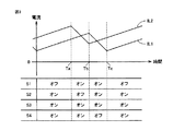
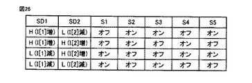
図7は、実施の形態1に従うデューティ比制御を説明するための図表である。図7には、デューティ比Db1およびDb2を、直流電源B2の出力制御のためのデューティ比Dbに設定する場合(Db1=Db2=Db)におけるデューティ比Da1,Da2の設定が示される。 FIG. 7 is a table for describing duty ratio control according to the first embodiment. FIG. 7 shows the setting of the duty ratios Da1 and Da2 when the duty ratios Db1 and Db2 are set to the duty ratio Db for output control of the DC power supply B2 (Db1 = Db2 = Db).
図7を参照して、第1のキャリア周期(全合わせ周期)では、デューティ比Da1およびデューティ比Db1の和が1となるように(Da1+Db1=1)、デューティ比Da1を調整する。デューティ比Da1は、下記(3)式に示すように、デューティ比Db1(=Db)に応じて設定される。 Referring to FIG. 7, in the first carrier period (all matching periods), duty ratio Da1 is adjusted so that the sum of duty ratio Da1 and duty ratio Db1 is 1 (Da1 + Db1 = 1). The duty ratio Da1 is set according to the duty ratio Db1 (= Db) as shown in the following equation (3).
Da1=1−Db1=1−Db ・・・(3)
第2のキャリア周期(昇圧比調整周期)では、デューティ比Da2は、1調整期間(m個のキャリア周期)を通算したデューティ比Daの平均値が、直流電源B1の出力制御のためのデューティ比Daに相当するように、デューティ比Da1に応じて設定される。デューティ比Da2は、下記(4)式に示すように、デューティ比Da1に応じて設定される。
Da1 = 1−Db1 = 1−Db (3)
In the second carrier cycle (step-up ratio adjustment cycle), the duty ratio Da2 is an average value of the duty ratio Da obtained by adding one adjustment period (m carrier cycles), and the duty ratio for output control of the DC power supply B1. It is set according to the duty ratio Da1 so as to correspond to Da. The duty ratio Da2 is set according to the duty ratio Da1, as shown in the following equation (4).
Da2=(mDa−nDa1)/(m−n)={mDa−n(1−Db)}/(m−n) ・・・(4)
なお、図5に示した動作例(m=2,n=1)では、(4)式に基づいて、デューティ比Da2は、デューティ比Da2=2×Da−(1−Db)に設定される。
Da2 = (mDa-nDa1) / (mn) = {mDa-n (1-Db)} / (mn) (4)
In the operation example (m = 2, n = 1) shown in FIG. 5, the duty ratio Da2 is set to the duty ratio Da2 = 2 × Da− (1−Db) based on the equation (4). .
ここで、図7から理解されるように、第1のキャリア周期における位相差φ1=180度である。一方、第2のキャリア周期における位相差φ2は、デューティ比Da2,Db2、すなわち、デューティ比Da,Dbに応じて変化する。このため、デューティ比Da,Dbと位相差φ2との関係を予め求めるとともに、その対応関係を予めマップ(以下、「位相差マップ」とも称する)あるいは関係式(以下、「位相差算出式」とも称する)として制御装置40に記憶することが可能である。
Here, as understood from FIG. 7, the phase difference φ1 = 180 degrees in the first carrier period. On the other hand, the phase difference φ2 in the second carrier period changes according to the duty ratios Da2 and Db2, that is, the duty ratios Da and Db. For this reason, the relationship between the duty ratios Da and Db and the phase difference φ2 is obtained in advance, and the corresponding relationship is previously determined as a map (hereinafter also referred to as “phase difference map”) or a relational expression (hereinafter referred to as “phase difference calculation formula”). Can be stored in the
そして、図5で説明した、パラレル接続モードにおける、直流電源B1,B2での電圧/電流制御のためのPWM制御において、算出されたデューティ比Da,Dbに基づいて、上記式(3)および式(4)を用いてデューティ比Da1,Da2を設定するとともに、デューティ比Db1,Db2を設定する。また、第1のキャリア周期における位相差φ1=180度に設定するとともに、位相差マップおよび位相差算出式に従って、デューティ比Da,Dbに基づいて位相差φ2を算出することができる。そして、1調整期間単位で、設定された位相差φ1,φ2を切換えてキャリア波CW1,CW2を発生させ、デューティ比Da1またはDa2とキャリア波CW1との比較に基づくPWM制御、およびデューティ比Db1またはDb2とキャリア波CW2との比較に基づくPWM制御を実行する。このようにして、上述した、スイッチング素子S1〜S4でのスイッチング損失を低減した高効率の直流電力変換を実現することができる。 Then, in the PWM control for voltage / current control in the DC power supplies B1 and B2 in the parallel connection mode described with reference to FIG. 5, based on the calculated duty ratios Da and Db, the above formula (3) and formula The duty ratios Da1 and Da2 are set using (4), and the duty ratios Db1 and Db2 are set. Further, the phase difference φ2 can be calculated based on the duty ratios Da and Db according to the phase difference map and the phase difference calculation formula, while setting the phase difference φ1 = 180 degrees in the first carrier period. Then, in one adjustment period unit, the set phase differences φ1 and φ2 are switched to generate carrier waves CW1 and CW2, and PWM control based on the comparison between the duty ratio Da1 or Da2 and the carrier wave CW1, and the duty ratio Db1 or PWM control based on a comparison between Db2 and carrier wave CW2 is executed. In this way, high-efficiency DC power conversion with reduced switching loss in the switching elements S1 to S4 described above can be realized.
なお、図5〜図7では、デューティ比Db1,Db2を直流電源B2の出力制御によって算出されるデューティ比Dbに設定し、デューティ比Da1,Da2を調整する場合を説明したが、デューティ比Da1,Da2を直流電源B1の出力制御のためのデューティ比Daに設定し、デューティ比Db1,Db2を調整する場合(第1の変形例)、または、デューティ比Da1,Da2およびDb1,Db2をそれぞれ調整する場合(第2の変形例)においても、同様のデューティ比制御およびキャリア位相制御を実行できる。 In FIGS. 5 to 7, the duty ratios Db1 and Db2 are set to the duty ratio Db calculated by the output control of the DC power supply B2, and the duty ratios Da1 and Da2 are adjusted. However, the duty ratio Da1, When Da2 is set to the duty ratio Da for output control of the DC power supply B1 and the duty ratios Db1 and Db2 are adjusted (first modification), or the duty ratios Da1 and Da2 and Db1 and Db2 are adjusted respectively. In the case (second modification), the same duty ratio control and carrier phase control can be executed.
(第1の変形例)
図8は、実施の形態1に従うデューティ比制御の第1の変形例を説明するための図表である。図8には、デューティ比Da1およびDa2を、直流電源B1の出力制御のためのデューティ比Daに設定する場合(Da1=Da2=Da)におけるデューティ比Db1,Db2の設定が示される。
(First modification)
FIG. 8 is a table for illustrating a first modification of the duty ratio control according to the first embodiment. FIG. 8 shows the setting of the duty ratios Db1 and Db2 when the duty ratios Da1 and Da2 are set to the duty ratio Da for output control of the DC power supply B1 (Da1 = Da2 = Da).
図8を参照して、第1のキャリア周期(全合わせ周期)では、デューティ比Da1およびデューティ比Db1の和が1となるように、デューティ比Db1を調整する。デューティ比Db1は、下記(5)式に示すように、デューティ比Da1(=Da)に応じて設定される。 Referring to FIG. 8, duty ratio Db1 is adjusted so that the sum of duty ratio Da1 and duty ratio Db1 becomes 1 in the first carrier period (all matching periods). The duty ratio Db1 is set according to the duty ratio Da1 (= Da) as shown in the following equation (5).
Db1=1−Da1=1−Da ・・・(5)
第2のキャリア周期(昇圧比調整周期)では、デューティ比Db2は、1調整期間(m個のキャリア周期)を通算したデューティ比Dbの平均値が、直流電源B2の出力制御のためのデューティ比Dbに一致するように、デューティ比Db1に応じて設定される。デューティ比Db2は、下記(6)式に示すように、デューティ比Db1に応じて設定される。
Db1 = 1-Da1 = 1-Da (5)
In the second carrier period (step-up ratio adjustment period), the duty ratio Db2 is an average value of the duty ratio Db obtained by adding one adjustment period (m carrier periods), and the duty ratio for output control of the DC power supply B2 It is set according to the duty ratio Db1 so as to coincide with Db. The duty ratio Db2 is set according to the duty ratio Db1, as shown in the following equation (6).
Db2=(mDb−nDb1)/(m−n)={mDb−n(1−Da)}/(m−n) ・・・(6)
図8に示した動作例(m=2,n=1)では、(6)式に基づいて、デューティ比Db2は、デューティ比Db2=2×Db−(1−Da)に設定される。
Db2 = (mDb-nDb1) / (mn) = {mDb-n (1-Da)} / (mn) (6)
In the operation example (m = 2, n = 1) shown in FIG. 8, the duty ratio Db2 is set to the duty ratio Db2 = 2 × Db− (1−Da) based on the equation (6).
なお、図8から理解されるように、第1のキャリア周期における位相差φ1=180度である。一方、第2のキャリア周期における位相差φ2は、位相差マップおよび位相差算出式に従って、デューティ比Da,Dbに基づいて算出される。 As can be understood from FIG. 8, the phase difference φ1 = 180 degrees in the first carrier period. On the other hand, the phase difference φ2 in the second carrier period is calculated based on the duty ratios Da and Db according to the phase difference map and the phase difference calculation formula.
(第2の変形例)
図9は、実施の形態1に従うデューティ比制御の第2の変形例を説明するための図表である。
(Second modification)
FIG. 9 is a table for describing a second modification of the duty ratio control according to the first embodiment.
図9を参照して、第1のキャリア周期(全合わせ周期)では、デューティ比Da1およびデューティ比Db1の和が1となるように、デューティ比Da1およびデューティ比Db1を調整する。デューティ比Da1は、下記式(7)に示すように、直流電源B1の出力制御のためのデューティ比Daと、デューティ比Db1を、直流電源B2の出力制御のためのデューティ比Dbに設定したときのデューティ比Da1(式(3)参照)とを、任意の比率r(0<r<1):(1−r)で足し合わせた値に設定される。 Referring to FIG. 9, duty ratio Da1 and duty ratio Db1 are adjusted so that the sum of duty ratio Da1 and duty ratio Db1 becomes 1 in the first carrier period (all matching periods). When the duty ratio Da1 is set to the duty ratio Da for output control of the DC power supply B1 and the duty ratio Db1 for output control of the DC power supply B2 as shown in the following formula (7), Is set to a value obtained by adding the duty ratio Da1 (see Expression (3)) at an arbitrary ratio r (0 <r <1) :( 1-r).
Da1=r×Da+(1−r)×(1−Db) ・・・(7)
デューティ比Db1は、下記式(8)に示すように、直流電源B2の出力制御のためのデューティ比Dbと、デューティ比Da1を、直流電源B1の出力制御のためのデューティ比Daに設定したときのデューティ比Db1(式(5)参照)とを、(1−r):rで足し合わせた値に設定される。
Da1 = r * Da + (1-r) * (1-Db) (7)
When the duty ratio Db1 is set to the duty ratio Db for output control of the DC power supply B2 and the duty ratio Da1 for output control of the DC power supply B1, as shown in the following formula (8), Is set to a value obtained by adding together (1−r): r.
Db1=(1−r)×Db+r×(1−Da) ・・・(8)
第2のキャリア周期(昇圧比調整周期)では、デューティ比Da2は、1調整期間を通算したデューティ比Daの平均値が、直流電源B1の出力制御のためのデューティ比Daに一致するように、デューティ比Da1に応じて設定される。デューティ比Da2は、下記(9)式に示すように、デューティ比Da1に応じて設定される。
Db1 = (1-r) × Db + r × (1-Da) (8)
In the second carrier cycle (step-up ratio adjustment cycle), the duty ratio Da2 is set so that the average value of the duty ratio Da for one adjustment period matches the duty ratio Da for output control of the DC power supply B1. It is set according to the duty ratio Da1. The duty ratio Da2 is set according to the duty ratio Da1, as shown in the following equation (9).
Da2=(mDa−nDa1)/(m−n)=[mDa−n{r×Da+(1−r)×(1−Db)}]/(m−n)・・・(9)
デューティ比Db2は、1調整期間を通算したデューティ比Dbの平均値が、直流電源B2の出力制御のためのデューティ比Dbに一致するように、デューティ比Db1に応じて設定される。デューティ比Db2は、下記(10)式に示すように、デューティ比Db1に応じて設定される。
Da2 = (mDa−nDa1) / (mn) = [mDa−n {r × Da + (1−r) × (1−Db)}] / (mn) (9)
The duty ratio Db2 is set according to the duty ratio Db1 so that the average value of the duty ratio Db obtained through one adjustment period coincides with the duty ratio Db for output control of the DC power supply B2. The duty ratio Db2 is set according to the duty ratio Db1, as shown in the following equation (10).
Db2=(mDb−nDb1)/(m−n)=[mDb−n{r×Db+(1−r)×(1−Da)}]/(m−n)・・・(10)
図10に示した動作例(m=2,n=1)において、r=0.5とした場合、デューティ比Da2={3×Da−(1−D2)}/2に設定される。また、デューティ比Db2={3×Db−(1−Da)}/2に設定される。
Db2 = (mDb−nDb1) / (mn) = [mDb−n {r × Db + (1−r) × (1−Da)}] / (mn) (10)
In the operation example shown in FIG. 10 (m = 2, n = 1), when r = 0.5, the duty ratio Da2 = {3 × Da− (1−D2)} / 2 is set. Further, the duty ratio Db2 = {3 × Db− (1−Da)} / 2 is set.
このように、第2の変形例では、デューティ比Da1およびDb1の間で、任意の比率rに従ってデューティ比の調整量を分配する。これにより、デューティ比Da1のみを調整する場合(図7参照)や、デューティ比Db1のみを調整する場合(図8参照)と比較して、リアクトル電流IL1,IL2の電流波形が、デューティ比制御が非実行であるときの電流波形から大きく変化してしまうのを防ぐことができる。 Thus, in the second modification, the duty ratio adjustment amount is distributed between the duty ratios Da1 and Db1 according to an arbitrary ratio r. Thereby, compared with the case where only the duty ratio Da1 is adjusted (see FIG. 7) or the case where only the duty ratio Db1 is adjusted (see FIG. 8), the current waveforms of the reactor currents IL1 and IL2 are It is possible to prevent a large change from the current waveform when it is not executed.
(直流電源の各動作状態におけるデューティ比制御およびキャリア位相制御)
図5〜図9では、直流電源B1およびB2の両方が力行の状態を説明したが、その他の状態においても、同様のデューティ比制御およびキャリア位相制御を実行できる。
(Duty ratio control and carrier phase control in each operating state of DC power supply)
Although FIGS. 5-9 demonstrated the state where both DC power supply B1 and B2 were power running, the same duty ratio control and carrier phase control can be performed also in another state.
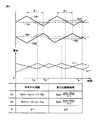
図10では、直流電源B1およびB2の両方が回生状態である。この状態では、第1のキャリア周期(全合わせ周期)において、リアクトル電流IL1の下降タイミングと、リアクトル電流IL2の上昇タイミングとが図中の時刻Taで重なり、かつ、リアクトル電流IL1の上昇タイミングと、リアクトル電流IL2の下降タイミングとが図中の時刻Tbで重なるような電流位相となるように、デューティ比Da1,Db2および位相差φ1を調整する。なお、直流電源B1およびB2の両方が回生状態である場合、リアクトル電流IL1の下降タイミングは、第1の電流経路から第2の電流経路へ切換えるときのリアクトル電流IL1の変曲点に相当し、リアクトル電流IL2の上昇タイミングは、第4の電流経路から第3の電流経路へ切換えるときのリアクトル電流IL2の変曲点に相当する。また、リアクトル電流IL1の上昇タイミングは、第2の電流経路から第1の電流経路へ切換えるときのリアクトル電流IL1の変曲点に相当し、リアクトル電流IL2の下降タイミングは、第3の電流経路から第4の電流経路へ切換えるときのリアクトル電流IL2の変曲点に相当する。 In FIG. 10, both DC power supplies B1 and B2 are in a regenerative state. In this state, in the first carrier cycle (all matching cycles), the fall timing of reactor current IL1 and the rise timing of reactor current IL2 overlap at time Ta in the figure, and the rise timing of reactor current IL1 The duty ratios Da1 and Db2 and the phase difference φ1 are adjusted so that the current phase overlaps with the falling timing of the reactor current IL2 at time Tb in the figure. When both DC power supplies B1 and B2 are in the regenerative state, the fall timing of reactor current IL1 corresponds to the inflection point of reactor current IL1 when switching from the first current path to the second current path, The rising timing of reactor current IL2 corresponds to the inflection point of reactor current IL2 when switching from the fourth current path to the third current path. The rising timing of reactor current IL1 corresponds to the inflection point of reactor current IL1 when switching from the second current path to the first current path, and the falling timing of reactor current IL2 is from the third current path. This corresponds to the inflection point of the reactor current IL2 when switching to the fourth current path.
図10には、デューティ比Db1,Db2を、直流電源B2の出力制御のためのデューティ比Dbに設定し、デューティ比Da1をデューティ比Db1(=Db)に応じて設定する例が示される。なお、図10から理解されるように、位相差φ1=180度である。これにより、時刻Taにおけるスイッチング素子S2のターンオン損失およびスイッチング素子S4のターンオフ損失を低減できる。さらに、時刻Tbにおけるスイッチング素子S4のターンオン損失およびスイッチング素子T2のターンオフ損失を低減できる。 FIG. 10 shows an example in which the duty ratios Db1 and Db2 are set to the duty ratio Db for output control of the DC power supply B2, and the duty ratio Da1 is set according to the duty ratio Db1 (= Db). As can be understood from FIG. 10, the phase difference φ1 = 180 degrees. Thereby, the turn-on loss of switching element S2 and the turn-off loss of switching element S4 at time Ta can be reduced. Furthermore, the turn-on loss of the switching element S4 and the turn-off loss of the switching element T2 at time Tb can be reduced.
第2のキャリア周期(昇圧比調整周期)では、1調整期間を通算したデューティ比Daの平均値が、直流電源B1の出力制御のためのデューティ比Daに相当するように、デューティ比Da2は、式(4)を用いて、デューティ比Da1に応じて設定される。さらに、リアクトル電流IL1の上昇タイミングと、リアクトル電流IL2の下降タイミングとが図中の時刻Teで重なるような電流位相となるように、位相差φ2を調整する。これにより、時刻Teにおけるスイッチング素子S4のターンオン損失およびスイッチング素子T2のターンオフ損失を低減できる。 In the second carrier cycle (step-up ratio adjustment cycle), the duty ratio Da2 is such that the average value of the duty ratio Da for one adjustment period corresponds to the duty ratio Da for output control of the DC power supply B1. Using equation (4), the duty ratio is set according to Da1. Furthermore, the phase difference φ2 is adjusted so that the rising timing of reactor current IL1 and the falling timing of reactor current IL2 have a current phase that overlaps at time Te in the drawing. Thereby, the turn-on loss of switching element S4 and the turn-off loss of switching element T2 at time Te can be reduced.
図11では、直流電源B1が回生状態である一方で、直流電源B2が力行状態である。この状態では、第1のキャリア周期(全合わせ周期)において、リアクトル電流IL1の上昇タイミングと、リアクトル電流IL2の上昇タイミングとが図中の時刻Taで重なりかつ、リアクトル電流IL1の下降タイミングと、リアクトル電流IL2の下降タイミングとが図中の時刻Tbで重なるような電流位相となるように、デューティ比Da1,Db2および位相差φ1を調整する。なお、直流電源B1が回生状態である一方で、直流電源B2が力行状態である場合、リアクトル電流IL1の上昇タイミングは、第2の電流経路から第1の電流経路へ切換えるときのリアクトル電流IL1の変曲点に相当し、リアクトル電流IL2の上昇タイミングは、第4の電流経路から第3の電流経路へ切換えるときのリアクトル電流IL2の変曲点に相当する。また、リアクトル電流IL1の下降タイミングは、第2の電流経路から第1の電流経路へ切換えるときのリアクトル電流IL1の変曲点に相当し、リアクトル電流IL2の下降タイミングは、第3の電流経路から第4の電流経路へ切換えるときのリアクトル電流IL2の変曲点に相当する。これにより、時刻Taにおけるスイッチング素子S1のターンオン損失およびスイッチング素子S3のターンオフ損失を低減できる。さらに、時刻Tbにおけるスイッチング素子S3のターンオン損失およびスイッチング素子S1のターンオフ損失を低減できる。 In FIG. 11, the DC power supply B1 is in the regenerative state, while the DC power supply B2 is in the powering state. In this state, the rise timing of reactor current IL1 and the rise timing of reactor current IL2 overlap at time Ta in the figure in the first carrier cycle (all matching cycles), and the fall timing of reactor current IL1 and the reactor The duty ratios Da1 and Db2 and the phase difference φ1 are adjusted so that the current phase overlaps with the falling timing of the current IL2 at time Tb in the figure. When DC power supply B1 is in the regenerative state and DC power supply B2 is in the powering state, the rising timing of reactor current IL1 is the level of reactor current IL1 when switching from the second current path to the first current path. It corresponds to the inflection point, and the rising timing of the reactor current IL2 corresponds to the inflection point of the reactor current IL2 when switching from the fourth current path to the third current path. The fall timing of reactor current IL1 corresponds to the inflection point of reactor current IL1 when switching from the second current path to the first current path, and the fall timing of reactor current IL2 is from the third current path. This corresponds to the inflection point of the reactor current IL2 when switching to the fourth current path. Thereby, the turn-on loss of switching element S1 and the turn-off loss of switching element S3 at time Ta can be reduced. Furthermore, the turn-on loss of switching element S3 and the turn-off loss of switching element S1 at time Tb can be reduced.
具体的には、第1のキャリア周期では、デューティ比Da1とデューティ比Db1とが等しくなるように、デューティ比Da1,Db1を調整する。図11には、デューティ比Db1およびDb2を、直流電源B2の出力制御のためのデューティ比Dbに設定する場合(Db1=Db2=Db)におけるデューティ比Da1,Da2の設定が示される。デューティ比Da1は、下記(11)式に示すように、デューティ比Db1(=Db)に応じて設定される。 Specifically, in the first carrier period, the duty ratios Da1 and Db1 are adjusted so that the duty ratio Da1 and the duty ratio Db1 are equal. FIG. 11 shows the setting of the duty ratios Da1 and Da2 when the duty ratios Db1 and Db2 are set to the duty ratio Db for output control of the DC power supply B2 (Db1 = Db2 = Db). The duty ratio Da1 is set according to the duty ratio Db1 (= Db) as shown in the following equation (11).
Da1=Db1=Db ・・・(11)
第2のキャリア周期(昇圧比調整周期)では、デューティ比Da2は、1調整期間(m個のキャリア周期)を通算したデューティ比Daの平均値が、直流電源B1の出力制御のためのデューティ比Daに一致するように、デューティ比Da1に応じて設定される。デューティ比Da2は、下記(12)式に示すように、デューティ比Da1に応じて設定される。
Da1 = Db1 = Db (11)
In the second carrier cycle (step-up ratio adjustment cycle), the duty ratio Da2 is an average value of the duty ratio Da obtained by adding one adjustment period (m carrier cycles), and the duty ratio for output control of the DC power supply B1. It is set according to the duty ratio Da1 so as to coincide with Da. The duty ratio Da2 is set according to the duty ratio Da1, as shown in the following equation (12).
Da2=(mDa−nDa1)/(m−n)={mDa−nDb)}/(m−n) ・・・(12)
図11に示した動作例(m=2,n=1)では、(12)式に基づいて、デューティ比Da2は、デューティ比Da2=2×Da−Dbに設定される。
Da2 = (mDa-nDa1) / (mn) = {mDa-nDb)} / (mn) (12)
In the operation example (m = 2, n = 1) shown in FIG. 11, the duty ratio Da2 is set to the duty ratio Da2 = 2 × Da−Db based on the equation (12).
図11から理解されるように、第1のキャリア周期における位相差φ1=0である。一方、第2のキャリア周期における位相差φ2は、予め制御装置40に記憶された位相差マップあるいは位相差算出式に従って、デューティ比Da,Dbに基づいて算出される。そして、1調整期間単位で、設定された位相差φ1,φ2を切換えてキャリア波CW1,CW2を発生させ、デューティ比Da1またはDa2とキャリア波CW1との比較に基づくPWM制御、およびデューティ比Db1またはDb2とキャリア波CW2との比較に基づくPWM制御を実行することにより、上述した、スイッチング素子S1〜S4でのスイッチング損失を低減した高効率の直流電力変換を実現することができる。
As understood from FIG. 11, the phase difference φ1 = 0 in the first carrier period. On the other hand, the phase difference φ2 in the second carrier period is calculated based on the duty ratios Da and Db according to a phase difference map or a phase difference calculation formula stored in the
なお、図11では、デューティ比Db1,Db2を直流電源B2の出力制御のためのデューティ比Dbに設定し、デューティ比Da1,Da2を調整する場合を説明したが、デューティ比Da1,Da2を直流電源B1の出力制御のためのデューティ比Daに設定し、デューティ比Db1,Db2を調整する場合(第3の変形例)、あるいは、デューティ比Da1,Da2およびDb1,Db2をそれぞれ調整する場合(第4の変形例)においても、同様のデューティ比制御およびキャリア位相制御を実行できる。 In FIG. 11, the duty ratios Db1 and Db2 are set to the duty ratio Db for output control of the DC power supply B2 and the duty ratios Da1 and Da2 are adjusted. When the duty ratio Da for output control of B1 is set and the duty ratios Db1 and Db2 are adjusted (third modified example), or when the duty ratios Da1, Da2 and Db1, Db2 are respectively adjusted (fourth) In the modified example), similar duty ratio control and carrier phase control can be executed.
(第3の変形例)
図12は、実施の形態1に従うデューティ比制御の第3の変形例を説明するための図表である。図12には、デューティ比Da1およびDa2を、直流電源B1の出力制御のためのデューティ比Daに設定する場合(Da1=D2=Da)におけるデューティ比Db1,Db2の設定が示される。
(Third Modification)
FIG. 12 is a table for illustrating a third modification of the duty ratio control according to the first embodiment. FIG. 12 shows the setting of the duty ratios Db1 and Db2 when the duty ratios Da1 and Da2 are set to the duty ratio Da for output control of the DC power supply B1 (Da1 = D2 = Da).
図12を参照して、第1のキャリア周期(全合わせ周期)では、デューティ比Da1とデューティ比Db1とが等しくなるように、デューティ比Db1を調整する。デューティ比Db1は、下記(13)式に示すように、デューティ比Da1(=Da)に応じて設定される。 Referring to FIG. 12, in the first carrier period (all matching periods), duty ratio Db1 is adjusted so that duty ratio Da1 and duty ratio Db1 are equal. The duty ratio Db1 is set according to the duty ratio Da1 (= Da) as shown in the following equation (13).
Db1=Da1=Da ・・・(13)
第2のキャリア周期(昇圧比調整周期)では、デューティ比Db2は、1調整期間(m個のキャリア周期)を通算したデューティ比Dbの平均値が、直流電源B2の出力制御のためのデューティ比Dbに一致するように、デューティ比Db1に応じて設定される。デューティ比Db2は、下記(14)式に示すように、デューティ比Db1に応じて設定される。
Db1 = Da1 = Da (13)
In the second carrier period (step-up ratio adjustment period), the duty ratio Db2 is an average value of the duty ratio Db obtained by adding one adjustment period (m carrier periods), and the duty ratio for output control of the DC power supply B2 It is set according to the duty ratio Db1 so as to coincide with Db. The duty ratio Db2 is set according to the duty ratio Db1, as shown in the following equation (14).
Db2=(mDb−nDb1)/(m−n)={mDb−nDa}/(m−n) ・・・(14)
図12に示した動作例(m=2,n=1)では、(14)式に基づいて、デューティ比Db2は、デューティ比Db2=2×Db−Daに設定される。
Db2 = (mDb−nDb1) / (mn) = {mDb−nDa} / (mn) (14)
In the operation example (m = 2, n = 1) shown in FIG. 12, the duty ratio Db2 is set to the duty ratio Db2 = 2 × Db−Da based on the equation (14).
なお、図12から理解されるように、第1のキャリア周期における位相差φ1=0である。一方、第2のキャリア周期における位相差φ2は、予め制御装置40に記憶された位相差マップあるいは位相差算出式に従って、デューティ比Da,Dbに基づいて算出される。
As can be understood from FIG. 12, the phase difference φ1 = 0 in the first carrier period. On the other hand, the phase difference φ2 in the second carrier period is calculated based on the duty ratios Da and Db according to a phase difference map or a phase difference calculation formula stored in the
(第4の変形例)
図13は、実施の形態1に従うデューティ比制御の第4の変形例を説明するための図表である。
(Fourth modification)
FIG. 13 is a chart for illustrating a fourth modification of the duty ratio control according to the first embodiment.
図13を参照して、第1のキャリア周期(全合わせ周期)では、デューティ比Da1とデューティ比Db1とが等しくなるように、デューティ比Da1およびデューティ比Db1を調整する。デューティ比Da1は、下記式(15)に示すように、直流電源B1の出力制御のためのデューティ比Daと、デューティ比Db1を、直流電源B2の出力制御のためのデューティ比Dbに設定したときのデューティ比Da1(式(11)参照)とを、任意の比率r:(1−r)で足し合わせた値に設定される。 Referring to FIG. 13, in the first carrier period (all matching periods), duty ratio Da1 and duty ratio Db1 are adjusted so that duty ratio Da1 and duty ratio Db1 are equal. When the duty ratio Da1 is set to the duty ratio Da for output control of the DC power supply B1 and the duty ratio Db1 for output control of the DC power supply B2 as shown in the following formula (15), Is set to a value obtained by adding the duty ratio Da1 (see Expression (11)) at an arbitrary ratio r: (1-r).
Da1=r×Da+(1−r)×Db ・・・(15)
デューティ比Db1は、下記式(16)に示すように、直流電源B2の出力制御のためのデューティ比Dbと、デューティ比Da1を、直流電源B1の出力制御のためのデューティ比Daに設定したときのデューティ比Db1(式(13)参照)とを、(1−r):rで足し合わせた値に設定される。
Da1 = r × Da + (1−r) × Db (15)
When the duty ratio Db1 is set to the duty ratio Db for output control of the DC power supply B2 and the duty ratio Da1 for output control of the DC power supply B1, as shown in the following equation (16), Is set to a value obtained by adding (1−r): r to the duty ratio Db1 (see Expression (13)).
Db1=(1−r)×Db+r×Da ・・・(16)
第2のキャリア周期(昇圧比調整周期)では、デューティ比Da2は、1調整期間を通算したデューティ比Daの平均値が、直流電源B1の出力制御のためのデューティ比Daに相当するように、デューティ比Da1に応じて設定される。デューティ比Da2は、下記(17)式に示すように、デューティ比Da1に応じて設定される。
Db1 = (1-r) × Db + r × Da (16)
In the second carrier cycle (step-up ratio adjustment cycle), the duty ratio Da2 is set so that the average value of the duty ratio Da for one adjustment period corresponds to the duty ratio Da for output control of the DC power supply B1. It is set according to the duty ratio Da1. The duty ratio Da2 is set according to the duty ratio Da1, as shown in the following equation (17).
Da2=(mDa−nDa1)/(m−n)=[mDa−n{r×Da+(1−r)×Db}]/(m−n)・・・(17)
デューティ比Db2は、1調整期間を通算したデューティ比Dbの平均値が、直流電源B2の出力制御のためのデューティ比Dbに相当するように、デューティ比Db1に応じて設定される。デューティ比Db2は、下記(18)式に示すように、デューティ比Db1に応じて設定される。
Da2 = (mDa−nDa1) / (mn) = [mDa−n {r × Da + (1−r) × Db}] / (mn) (17)
The duty ratio Db2 is set according to the duty ratio Db1 so that the average value of the duty ratio Db for one adjustment period corresponds to the duty ratio Db for output control of the DC power supply B2. The duty ratio Db2 is set according to the duty ratio Db1, as shown in the following equation (18).
Db2=(mDb−nDb1)/(m−n)=[mDb−n{(1−r)×Db+r×Da)}]/(m−n)・・・(18)
図13に示した動作例(m=2,n=1)において、r=0.5とした場合、デューティ比Da1=Db1=(Da+Db)/2に設定される。また、デューティ比Da2=(b2=(3×Da−Da)/2に設定され、デューティ比Db2=(−Da+3×Db)/3に設定される。
Db2 = (mDb−nDb1) / (mn) = [mDb−n {(1-r) × Db + r × Da)}] / (mn) (18)
In the operation example shown in FIG. 13 (m = 2, n = 1), when r = 0.5, the duty ratio Da1 = Db1 = (Da + Db) / 2 is set. Further, the duty ratio Da2 = (b2 = (3 × Da−Da) / 2 is set, and the duty ratio Db2 = (− Da + 3 × Db) / 3 is set.
図14では、直流電源B1が力行状態である一方で、直流電源B2が回生状態である。この状態では、第1のキャリア周期(全合わせ周期)において、リアクトル電流IL1の下降タイミングと、リアクトル電流IL2の下降タイミングとが図中の時刻Taで重なり、かつ、リアクトル電流IL1の上昇タイミングと、リアクトル電流IL2の上昇タイミングとが図中の時刻Tbで重なるような電流位相となるように、デューティ比Da1,Db2および位相差φ1を調整する。なお、直流電源B1が力行状態である一方で、直流電源B2が回生状態である場合、リアクトル電流IL1の下降タイミングは、第1の電流経路から第2の電流経路へ切換えるときのリアクトル電流IL1の変曲点に相当し、リアクトル電流IL2の下降タイミングは、第3の電流経路から第4の電流経路へ切換えるときのリアクトル電流IL2の変曲点に相当する。また、リアクトル電流IL1の上昇タイミングは、第2の電流経路から第1の電流経路へ切換えるときのリアクトル電流IL1の変曲点に相当し、リアクトル電流IL2の上昇タイミングは、第4の電流経路から第3の電流経路へ切換えるときのリアクトル電流IL2の変曲点に相当する。これにより、時刻Taにおけるスイッチング素子S3のターンオン損失およびスイッチング素子S1のターンオフ損失を低減できる。さらに、時刻Tbにおけるスイッチング素子S1のターンオン損失およびスイッチング素子S3のターンオフ損失を低減できる。 In FIG. 14, the DC power source B1 is in a power running state, while the DC power source B2 is in a regenerative state. In this state, in the first carrier cycle (all matching cycles), the fall timing of reactor current IL1 and the fall timing of reactor current IL2 overlap at time Ta in the figure, and the rise timing of reactor current IL1 The duty ratios Da1 and Db2 and the phase difference φ1 are adjusted so that the current phase overlaps the rising timing of the reactor current IL2 at time Tb in the figure. When DC power supply B1 is in the power running state and DC power supply B2 is in the regenerative state, the descending timing of reactor current IL1 is the level of reactor current IL1 when switching from the first current path to the second current path. It corresponds to an inflection point, and the descending timing of the reactor current IL2 corresponds to an inflection point of the reactor current IL2 when switching from the third current path to the fourth current path. The rising timing of reactor current IL1 corresponds to the inflection point of reactor current IL1 when switching from the second current path to the first current path, and the rising timing of reactor current IL2 is from the fourth current path. This corresponds to the inflection point of the reactor current IL2 when switching to the third current path. Thereby, the turn-on loss of switching element S3 and the turn-off loss of switching element S1 at time Ta can be reduced. Furthermore, the turn-on loss of the switching element S1 and the turn-off loss of the switching element S3 at time Tb can be reduced.
なお、図14には、デューティ比Db1,Db2を、直流電源B2の出力制御のためのデューティ比Dbに設定し(Db1=Db2=Db)、デューティ比Da1をデューティ比Db1(=Db)に応じて設定する例が示される。図14から理解されるように、位相差φ1=0である。 In FIG. 14, the duty ratios Db1 and Db2 are set to the duty ratio Db for output control of the DC power supply B2 (Db1 = Db2 = Db), and the duty ratio Da1 is set according to the duty ratio Db1 (= Db). An example of setting is shown. As understood from FIG. 14, the phase difference φ1 = 0.
第2のキャリア周期(昇圧比調整周期)では、1調整期間を通算したデューティ比Daの平均値が、直流電源B1の出力制御のためのデューティ比Daに一致するように、デューティ比Da2は、式(12)を用いて、デューティ比Da1に応じて設定される。さらに、リアクトル電流IL1の上昇タイミングと、リアクトル電流IL2の上昇タイミングとが図中の時刻Teで重なるような電流位相となるように、位相差φ2を調整する。これにより、時刻Teにおけるスイッチング素子S1のターンオン損失およびスイッチング素子S3のターンオフ損失を低減できる。 In the second carrier cycle (step-up ratio adjustment cycle), the duty ratio Da2 is set so that the average value of the duty ratio Da for one adjustment period coincides with the duty ratio Da for output control of the DC power supply B1. Using the equation (12), it is set according to the duty ratio Da1. Further, the phase difference φ2 is adjusted so that the rising timing of reactor current IL1 and the rising timing of reactor current IL2 have a current phase that overlaps at time Te in the drawing. Thereby, the turn-on loss of switching element S1 and the turn-off loss of switching element S3 at time Te can be reduced.
このように、直流電源B1およびB2の力行/回生状態の組み合わせによって、第1のキャリア周期(全合わせ周期)におけるデューティ比Da1,Db1および位相差φ1、および第2のキャリア周期(昇圧比調整周期)におけるデューティ比Da2,Db2および位相差φ2が異なる。したがって、力行/回生状態の組み合わせごとに、上述した、デューティ比算出式を設定するとともに、位相差マップまたは位相差算出式を設定することが好ましい。 As described above, the duty ratios Da1 and Db1 and the phase difference φ1 and the second carrier period (step-up ratio adjustment period) in the first carrier period (all alignment periods) are determined by the combination of the power running / regenerative state of the DC power supplies B1 and B2. ) Are different in duty ratio Da2, Db2 and phase difference φ2. Therefore, it is preferable to set the above-described duty ratio calculation formula and set the phase difference map or the phase difference calculation formula for each combination of power running / regenerative state.
このように、実施の形態1に従う電力変換器50におけるデューティ比制御およびキャリア位相制御では、電力変換器50の動作状態、具体的には、直流電源B1,B2の電流/電圧制御のためのデューティ比、および直流電源B1,B2の力行/回生状態に応じて、直流電源B1,B2のデューティ比およびキャリア波CW1,CW2の間の位相差φを調整する。特に、1調整期間単位で図6および図8から図14に示した電流位相が実現されるように、デューティ比および位相差φを調整することによって、電力変換器50の動作状態の変化に対応させて、直流電源B1およびB2間の電力配分に影響を及ぼすことなく、スイッチング素子S1〜S4のスイッチング損失が低減された高効率の直流電力変換を実行することができる。
Thus, in duty ratio control and carrier phase control in
[実施の形態2]
上述のように、実施の形態1に従うデューティ比制御およびキャリア位相制御によれば、電力変換器50をパラレル接続モードで動作させる場合のスイッチング素子S1〜S4のスイッチング損失を低減させることが可能である。実施の形態1に従うデューティ比制御およびキャリア位相制御は、電力変換器50と回路構成が異なる電力変換器に対しても適用することが可能である。
[Embodiment 2]
As described above, according to the duty ratio control and the carrier phase control according to the first embodiment, it is possible to reduce the switching loss of switching elements S1 to S4 when
実施の形態2では、電力変換器50と回路構成が異なる電力変換器における制御動作、特にデューティ比制御およびキャリア位相制御について説明する。
In the second embodiment, a control operation in a power converter having a circuit configuration different from that of the
(回路構成)
図15は、本発明の実施の形態2に従う電源システムの構成を示す回路図である。
(Circuit configuration)
FIG. 15 is a circuit diagram showing a configuration of a power supply system according to the second embodiment of the present invention.
図15を参照して、電源システム5Aは、直流電源B1と、直流電源B2と、電力変換器10と、制御装置40Aとを備える。実施の形態2に従う電源システム5Aは、図1に示された電源システム5と比較して、電力変換器50および制御装置40に代えて、電力変換器10および制御装置40Aを備える。なお、直流電源B1およびB2は、「第1の直流電源」および「第2の直流電源」にそれぞれ対応する。
Referring to FIG. 15,
電力変換器10は、高電圧側の電力線PLおよび低電圧側の電力線GLの間の直流電圧VH(出力電圧VH)を制御するように構成される。電力線GLは、代表的には、接地配線で構成される。
The
電力変換器10は、電力用半導体スイッチング素子S1〜S5と、リアクトルL1,L2とを含む。本実施の形態において、電力用半導体スイッチング素子(スイッチング素子)としては、IGBT、電力用MOSトランジスタあるいは電力用バイポーラトランジスタ等を用いることができる。
スイッチング素子S1〜S5は、制御装置40Aからの制御信号SG1〜SG5にそれぞれ応答して、オンオフを制御することが可能である。具体的には、スイッチング素子S1〜S5は、制御信号SG1〜SG5がHレベルのときにオン状態となって、電流経路を形成可能な状態となる。一方で、スイッチング素子S1〜S5は、制御信号SG1〜SG5がLレベルのときにオフ状態となって、当該電流経路を遮断する状態となる。
Switching elements S1 to S5 can be turned on and off in response to control signals SG1 to SG5 from
スイッチング素子S1〜S4に対しては、逆並列ダイオードD1〜D4がそれぞれ配置されている。ダイオードD1〜D4は、順バイアス時に、電力線GLから電力線PLへ向かう方向(図中、下から上へ向かう方向)の電流経路を形成するように配置される。一方で、ダイオードD1〜D4は、逆バイアス時には、当該電流経路を非形成とする。具体的には、ダイオードD1は、ノードN1から電力線PLへ向かう方向を順方向とするように接続され、ダイオードD2は、電力線GLからノードN1へ向かう方向を順方向とするように接続される。同様に、ダイオードD3は、電力線GLからノードN2へ向かう方向を順方向とするように接続され、ダイオードD4は、ノードN2から電力線PLへ向かう方向を順方向とするように接続される。 Anti-parallel diodes D1 to D4 are arranged for switching elements S1 to S4, respectively. The diodes D1 to D4 are arranged so as to form a current path in a direction from the power line GL to the power line PL (a direction from the bottom to the top in the drawing) during forward bias. On the other hand, the diodes D1 to D4 do not form the current path during reverse bias. Specifically, diode D1 is connected so that the direction from node N1 toward power line PL is the forward direction, and diode D2 is connected so that the direction from power line GL toward node N1 is the forward direction. Similarly, diode D3 is connected so that the direction from power line GL toward node N2 is the forward direction, and diode D4 is connected so that the direction from node N2 toward power line PL is the forward direction.
スイッチング素子S1は、電力線PLおよびノードN1の間に電気的に接続される。リアクトルL1および直流電源B1は、ノードN1および電力線GLの間に直列に、電気的に接続される。たとえば、リアクトルL1は、直流電源B1の正極端子およびノードN1の間に電気的に接続されるとともに、直流電源B1の負極端子は、電力線GLと電気的に接続される。スイッチング素子S2は、ノードN1および電力線GLの間に電気的に接続される。なお、リアクトルL1および直流電源B1の接続順序を入れ換えても、電気的には等価な回路構成が維持される。 Switching element S1 is electrically connected between power line PL and node N1. Reactor L1 and DC power supply B1 are electrically connected in series between node N1 and power line GL. For example, reactor L1 is electrically connected between the positive terminal of DC power supply B1 and node N1, and the negative terminal of DC power supply B1 is electrically connected to power line GL. Switching element S2 is electrically connected between node N1 and power line GL. Even if the connection order of the reactor L1 and the DC power supply B1 is changed, an electrically equivalent circuit configuration is maintained.
スイッチング素子S3は、ノードN2および電力線GLの間に電気的に接続される。スイッチング素子S4は、電力線PLおよびノードN2の間に電気的に接続される。スイッチング素子S5は、ノードN1およびN2の間に電気的に接続される。リアクトルL2および直流電源B2は、電力線PLおよびノードN2の間に直列に、電気的に接続される。たとえば、リアクトルL2は、直流電源B2の正極端子および電力線PLの間に電気的に接続されるとともに、直流電源B2の負極端子は、ノードN2と電気的に接続される。なお、リアクトルL2および直流電源B2の接続順序を入れ換えても、電気的には等価な回路構成が維持される。 Switching element S3 is electrically connected between node N2 and power line GL. Switching element S4 is electrically connected between power line PL and node N2. Switching element S5 is electrically connected between nodes N1 and N2. Reactor L2 and DC power supply B2 are electrically connected in series between power line PL and node N2. For example, reactor L2 is electrically connected between the positive terminal of DC power supply B2 and power line PL, and the negative terminal of DC power supply B2 is electrically connected to node N2. Even if the connection order of reactor L2 and DC power supply B2 is changed, an electrically equivalent circuit configuration is maintained.
図15の構成例では、スイッチング素子S1およびダイオードD1は「第1の半導体素子」に対応し、スイッチング素子S2およびダイオードD2は「第2の半導体素子」に対応し、スイッチング素子S3およびダイオードD3は「第3の半導体素子」に対応する。さらに、スイッチング素子S4およびダイオードD4は「第4の半導体素子」に対応し、スイッチング素子S5は「第5の半導体素子」に対応する。また、スイッチング素子S1は「第1のスイッチング素子」に対応し、スイッチング素子S2は「第2のスイッチング素子」に対応し、スイッチング素子S3は「第3のスイッチング素子」に対応し、スイッチング素子S4は「第4のスイッチング素子」に対応し、スイッチング素子S5は「第5のスイッチング素子」に対応する。さらに、リアクトルL1およびL2は、「第1のリアクトル」および「第2のリアクトル」にそれぞれ対応する。図15の例では、スイッチング素子S1〜S5のオンオフ制御により、第1〜第5の半導体素子の各々において、電流経路の形成および遮断を制御することができる。 In the configuration example of FIG. 15, switching element S1 and diode D1 correspond to “first semiconductor element”, switching element S2 and diode D2 correspond to “second semiconductor element”, and switching element S3 and diode D3 are This corresponds to “third semiconductor element”. Further, the switching element S4 and the diode D4 correspond to a “fourth semiconductor element”, and the switching element S5 corresponds to a “fifth semiconductor element”. The switching element S1 corresponds to a “first switching element”, the switching element S2 corresponds to a “second switching element”, the switching element S3 corresponds to a “third switching element”, and the switching element S4 Corresponds to a “fourth switching element”, and the switching element S5 corresponds to a “fifth switching element”. Furthermore, reactors L1 and L2 correspond to a “first reactor” and a “second reactor”, respectively. In the example of FIG. 15, the formation and interruption of the current path can be controlled in each of the first to fifth semiconductor elements by the on / off control of the switching elements S1 to S5.
制御装置40Aは、たとえば、図示しないCPUおよびメモリを有する電子制御ユニット(ECU)によって構成される。制御装置40Aは、メモリに記憶されたマップおよびプログラムに基づいて、各センサによる検出値を用いた演算処理を行なうように構成される。あるいは、制御装置40Aの少なくとも一部は、電子回路等のハードウェアにより所定の数値・論理演算処理を実行するように構成されてもよい。
The
制御装置40Aは、出力電圧VHを制御するために、スイッチング素子S1〜S5のオンオフを制御する制御信号SG1〜SG5を生成する。なお、図15では図示を省略しているが、直流電源B1の電圧V[1]および電流I[1]、直流電源B2の電圧V[2]および電流I[2]、ならびに、出力電圧VHの検出器(電圧センサ)が設けられている。これらの検出器の出力は、制御装置40Aへ与えられる。
The
(電力変換器の動作)
実施の形態2に従う電力変換器10は、実施の形態1に従う電力変換器50と同様に、直流電源B1,B2と電力線PL,GLとの間での直流電力変換(DC/DC変換)の態様が異なる複数の動作モードを有する。これらの動作モードは、スイッチング素子のオンオフ制御の態様を切換えることによって選択的に適用される。
(Operation of power converter)
Similarly to
電力変換器10の複数の動作モードには、直流電源B1およびB2と電力線PL,GLとの間で並列にDC/DC変換を行なうための「パラレル昇圧モード」と、直列接続された直流電源B1およびB2と電力線PL,GLとの間でDC/DC変換を行なうための「シリーズ昇圧モード」とが含まれる。パラレル昇圧モードは、実施の形態1および特許文献1での「パラレル接続モード」に対応し、シリーズ昇圧モードは、実施の形態1および特許文献1での「シリーズ接続モード」に対応する。実施の形態2では、基本となるパラレル昇圧モードでの動作について説明する。
The plurality of operation modes of
(パラレル昇圧モードでの回路動作)
次に、電力変換器10のパラレル昇圧モードにおける動作および制御について詳細に説明する。電力変換器10は、パラレル昇圧モードにおいては、直流電源B1およびB2の各々に対して2つの昇圧チョッパ回路を並列に動作させる態様により動作する。すなわち、電力変換器10は、実施の形態1でのパラレル接続モードと同様に、直流電源B1およびB2と電力線PL,GL(負荷30)との間で並列なDC/DC変換を行なうことにより、電圧指令値VH*に従って出力電圧VHを制御する。
(Circuit operation in parallel boost mode)
Next, the operation and control of the
図15を参照して、電力変換器10においては、スイッチング素子S5をオンした場合と、オフした場合との間で、直流電源B1およびB2に対して形成される昇圧チョッパ回路が異なることが特徴である。
Referring to FIG. 15, in
電力変換器10において、スイッチング素子S5のオフ時には、ノードN1およびN2が電気的に切り離される。このときの電力変換器10の等価回路が図16に示される。
In
図16を参照して、スイッチング素子S5のオフ時には、直流電源B1に対して、スイッチング素子S2およびダイオードD2を下アームとし、スイッチング素子S1およびダイオードD1を上アームとする昇圧チョッパ回路が形成される。 Referring to FIG. 16, when switching element S5 is off, a step-up chopper circuit having switching element S2 and diode D2 as the lower arm and switching element S1 and diode D1 as the upper arm is formed with respect to DC power supply B1. .
一方、直流電源B2に対しては、スイッチング素子S4およびダイオードD4を下アームとし、スイッチング素子S3およびダイオードD3を上アームとする昇圧チョッパ回路が形成される。 On the other hand, for DC power supply B2, a boost chopper circuit is formed with switching element S4 and diode D4 as the lower arm and switching element S3 and diode D3 as the upper arm.
図17には、図16に示した等価回路図において、直流電源B1,B2の下アームオン時における電流経路が示される。 FIG. 17 shows a current path when the lower arms of DC power supplies B1 and B2 are turned on in the equivalent circuit diagram shown in FIG.
図17を参照して、スイッチング素子S2をオンすることにより、直流電源B1の出力によりリアクトルL1にエネルギを蓄積するための電流経路111(第1の電流経路)が形成される。すなわち、スイッチング素子S2は、直流電源B1に対応して形成される昇圧チョッパ回路の下アームに相当する。 Referring to FIG. 17, by turning on switching element S2, current path 111 (first current path) for storing energy in reactor L1 is formed by the output of DC power supply B1. That is, switching element S2 corresponds to the lower arm of the boost chopper circuit formed corresponding to DC power supply B1.
同様に、スイッチング素子S4をオンすることにより、直流電源B2の出力によりリアクトルL2にエネルギを蓄積するための電流経路112(第3の電流経路)が形成される。すなわち、スイッチング素子S4は、直流電源B2に対応して形成される昇圧チョッパ回路の下アームに相当する。 Similarly, by turning on the switching element S4, a current path 112 (third current path) for storing energy in the reactor L2 by the output of the DC power supply B2 is formed. That is, switching element S4 corresponds to the lower arm of the boost chopper circuit formed corresponding to DC power supply B2.
図18には、図16に示した等価回路図において、直流電源B1,B2の上アームオン時における電流経路が示される。 FIG. 18 shows a current path when the upper arms of DC power supplies B1 and B2 are turned on in the equivalent circuit diagram shown in FIG.
図18を参照して、スイッチング素子S2をオフすることにより、スイッチング素子S1またはダイオードD1を経由して、リアクトルL1の蓄積エネルギを直流電源B1からのエネルギとともに電力線PLへ出力するための電流経路113(第2の電流経路)が形成される。実施の形態2では、スイッチング素子S1およびS2を相補的にオンオフすることにより、スイッチング素子S2のオフ期間にスイッチング素子S1がオンされる。スイッチング素子S1は、直流電源B1に対応して形成される昇圧チョッパ回路の上アームに相当する。
Referring to FIG. 18, by turning off switching element S2,
同様に、スイッチング素子S4をオフすることにより、スイッチング素子S3またはダイオードD3を経由して、リアクトルL2の蓄積エネルギを直流電源B2からのエネルギとともに電力線PLへ出力するための電流経路114(第4の電流経路)が形成される。実施の形態2では、スイッチング素子S3およびS4を相補的にオンオフするので、スイッチング素子S4のオフ期間にスイッチング素子S3がオンする。スイッチング素子S3は、直流電源B2に対応して形成される昇圧チョッパ回路の上アームに相当する。 Similarly, by turning off switching element S4, current path 114 (fourth fourth) for outputting the stored energy of reactor L2 to power line PL together with the energy from DC power supply B2 via switching element S3 or diode D3. Current path) is formed. In the second embodiment, switching elements S3 and S4 are turned on and off in a complementary manner, so that switching element S3 is turned on during the off period of switching element S4. Switching element S3 corresponds to the upper arm of the step-up chopper circuit formed corresponding to DC power supply B2.
図17および図18から理解されるように、電流経路111および113を交互に形成することによって、直流電源B1および電力線PL,GLの間のDC/DC変換が実行される。同様に、電流経路112および114を交互に形成することによって、直流電源B2および電力線PL,GLの間のDC/DC変換が実行される。
As understood from FIGS. 17 and 18, DC / DC conversion between DC power supply B1 and power lines PL and GL is performed by alternately forming
以下では、直流電源B1に対応して形成される昇圧チョッパ回路の上アームを「B1Uアーム」とも称し、下アームを「B1Lアーム」と称する。同様に、直流電源B2に対応して形成される昇圧チョッパ回路の上アームを「B2Uアーム」とも称し、下アームを「B2Lアーム」とも称する。 Hereinafter, the upper arm of the boost chopper circuit formed corresponding to the DC power supply B1 is also referred to as “B1U arm”, and the lower arm is referred to as “B1L arm”. Similarly, the upper arm of the step-up chopper circuit formed corresponding to the DC power supply B2 is also referred to as “B2U arm”, and the lower arm is also referred to as “B2L arm”.
B1Lアームは、直流電源B1が力行状態のときにリアクトルL1にエネルギを蓄積するための「第1の電流経路」を形成する一方、直流電源B1が回生状態のときにリアクトルL1の蓄積エネルギを直流電源B1に出力するための「第2の電流経路」を形成する。B1Uアームは、直流電源B1が力行状態のときにリアクトルL1の蓄積エネルギを直流電源B1のエネルギとともに電力線PLに出力するための「第2の電流経路」を形成する一方で、直流電源B1が回生状態のときに電力線PLからの出力をリアクトルL1にエネルギを蓄積するための「第1の電流経路」を形成する。 The B1L arm forms a “first current path” for storing energy in the reactor L1 when the DC power supply B1 is in the power running state, while the DC L1 stores the energy stored in the reactor L1 when the DC power supply B1 is in the regenerative state. A “second current path” for outputting to the power supply B1 is formed. The B1U arm forms a “second current path” for outputting the stored energy of the reactor L1 to the power line PL together with the energy of the DC power supply B1 when the DC power supply B1 is in a power running state, while the DC power supply B1 is regenerated. A “first current path” is formed for storing energy in the reactor L1 from the output from the power line PL in the state.
また、B2Lアームは、直流電源B2が力行状態のときにリアクトルL2にエネルギを蓄積するための「第3の電流経路」を形成する一方、直流電源B2が回生状態のときにリアクトルL2の蓄積エネルギを直流電源B2に出力するための「第4の電流経路」を形成する。B2Uアームは、直流電源B2が力行状態のときにリアクトルL2の蓄積エネルギを直流電源B2のエネルギとともに電力線PLに出力するための「第3の電流経路」を形成する一方で、直流電源B2が回生状態のときに電力線PLからの出力をリアクトルL2にエネルギを蓄積するための「第4の電流経路」を形成する。なお、スイッチング素子S1〜S5の各々は、第1および第2の電流経路のいずれか一方と、第3および第4の電流経路のいずれか一方との両方に含まれるように配置される。 Further, the B2L arm forms a “third current path” for storing energy in the reactor L2 when the DC power supply B2 is in a power running state, while the stored energy of the reactor L2 when the DC power supply B2 is in a regenerative state. Is formed as a “fourth current path”. The B2U arm forms a “third current path” for outputting the accumulated energy of the reactor L2 to the power line PL together with the energy of the DC power supply B2 when the DC power supply B2 is in a power running state, while the DC power supply B2 is regenerated. In the state, a “fourth current path” is formed for accumulating energy in output from power line PL in reactor L2. Note that each of the switching elements S1 to S5 is disposed so as to be included in both one of the first and second current paths and either one of the third and fourth current paths.
図17から理解されるように、B1LアームおよびB2Lアームの形成時には、ノードN2からN1へ向かう電流経路が形成されると、電力線PLから電力線GLへの短絡経路が形成されてしまうため、当該電流経路を遮断する必要がある。同様に、図18から理解されるように、B1UアームおよびB2Uアームの形成時には、ノードN1からN2へ向かう電流経路が形成されると、電力線PLから電力線GLへの短絡経路が形成されてしまうため、当該電流経路を遮断する必要がある。したがって、B1LアームおよびB2Lアームの形成時、および、B1UアームおよびB2Uアームの形成時の各々では、スイッチング素子S5をオフすることによって、上記短絡経路の形成を回避することができる。 As understood from FIG. 17, when the current path from the node N2 to N1 is formed when the B1L arm and the B2L arm are formed, a short circuit path from the power line PL to the power line GL is formed. The route needs to be blocked. Similarly, as can be understood from FIG. 18, when forming the B1U arm and the B2U arm, if a current path from the node N1 to N2 is formed, a short circuit path from the power line PL to the power line GL is formed. It is necessary to interrupt the current path. Therefore, when the B1L arm and the B2L arm are formed and when the B1U arm and the B2U arm are formed, the switching element S5 is turned off to avoid the formation of the short-circuit path.
一方で、電力変換器10では、スイッチング素子S5のオン時には、ノードN1およびN2が電気的に接続される。このときの電力変換器10の等価回路が図19に示される。
On the other hand, in
図19を参照して、直流電源B1に関して、スイッチング素子S5によってノードN2がノードN1と電気的に接続されるので、ノードN2および電力線GLの間に接続されたスイッチング素子S3を、直流電源B1の下アーム(B1Lアーム)として昇圧チョッパ回路を形成することができる。同様に、ノードN2および電力線PLの間に電気的に接続されたスイッチング素子S4を直流電源B1の上アーム(B1Uアーム)として、昇圧チョッパ回路を形成することができる。 Referring to FIG. 19, since node N2 is electrically connected to node N1 by switching element S5 with respect to DC power supply B1, switching element S3 connected between node N2 and power line GL is connected to DC power supply B1. A step-up chopper circuit can be formed as the lower arm (B1L arm). Similarly, a step-up chopper circuit can be formed using switching element S4 electrically connected between node N2 and power line PL as the upper arm (B1U arm) of DC power supply B1.
また、直流電源B2に対しては、ノードN1および電力線PLの間に接続されたスイッチング素子S1を下アーム(B2Lアーム)とし、スイッチング素子S2を上アーム(B2Uアーム)とした昇圧チョッパ回路を形成することができる。 For DC power supply B2, a step-up chopper circuit is formed in which switching element S1 connected between node N1 and power line PL is the lower arm (B2L arm) and switching element S2 is the upper arm (B2U arm). can do.
図20には、図19に示した等価回路図において、直流電源B1,B2の下アームオン時における電流経路が示される。 FIG. 20 shows a current path when the lower arms of DC power supplies B1 and B2 are turned on in the equivalent circuit diagram shown in FIG.
図20(a)を参照して、スイッチング素子S3,S5をオンすることにより、直流電源B1の出力によりリアクトルL1にエネルギを蓄積するための電流経路115(第1の電流経路)が形成される。一方で、図20(b)に示されるように、スイッチング素子S1,S5をオンすることにより、直流電源B2の出力によりリアクトルL2にエネルギを蓄積するための電流経路116(第3の電流経路)が形成される。 Referring to FIG. 20A, by turning on switching elements S3 and S5, current path 115 (first current path) for storing energy in reactor L1 is formed by the output of DC power supply B1. . On the other hand, as shown in FIG. 20B, a current path 116 (third current path) for storing energy in the reactor L2 by the output of the DC power supply B2 by turning on the switching elements S1 and S5. Is formed.
図21には、図19に示した等価回路図において、直流電源B1,B2の上アームオン時における電流経路が示される。 FIG. 21 shows a current path when the upper arms of DC power supplies B1 and B2 are turned on in the equivalent circuit diagram shown in FIG.
図21(a)を参照して、直流電源B1に関して、スイッチング素子S5がオンされた状態でスイッチング素子S3をオフすることにより、スイッチング素子S4またはダイオードD4を経由してリアクトルL1の蓄積エネルギを直流電源B1からのエネルギとともに電力線PLへ出力するための電流経路117(第2の電流経路)が形成される。上述のように、スイッチング素子S3およびS4は相補的にオンオフされるので、スイッチング素子S3によってB1Lアームを形成するとともに、スイッチング素子S4によってB1Uアームを形成することができる。 Referring to FIG. 21 (a), with respect to DC power supply B1, switching element S3 is turned off while switching element S5 is turned on, so that the stored energy of reactor L1 is changed to DC via switching element S4 or diode D4. A current path 117 (second current path) for outputting to power line PL together with energy from power supply B1 is formed. As described above, since the switching elements S3 and S4 are turned on and off in a complementary manner, the switching element S3 can form the B1L arm and the switching element S4 can form the B1U arm.
図21(b)を参照して、直流電源B2に関しては、スイッチング素子S5がオンされた状態でスイッチング素子S1をオフすることにより、スイッチング素子S2またはダイオードD2を経由してリアクトルL2の蓄積エネルギを直流電源B2からのエネルギとともに電力線PLへ出力するための電流経路118(第4の電流経路)が形成される。上述のように、スイッチング素子S1およびS2は相補的にオンオフされるので、スイッチング素子S1によってB2Lアームを形成するとともに、スイッチング素子S2によってB2Uアームを形成することができる。 Referring to FIG. 21B, with respect to DC power supply B2, by turning off switching element S1 while switching element S5 is on, the stored energy of reactor L2 is reduced via switching element S2 or diode D2. A current path 118 (fourth current path) is formed for output to power line PL together with energy from DC power supply B2. As described above, since the switching elements S1 and S2 are turned on and off in a complementary manner, the B2L arm can be formed by the switching element S1, and the B2U arm can be formed by the switching element S2.
図22には、スイッチング素子S5のオフ時およびオン時にそれぞれ形成される昇圧チョッパ回路の各アームとスイッチング素子のオンオフとの対応関係が示される。 FIG. 22 shows the correspondence between each arm of the step-up chopper circuit formed when the switching element S5 is turned off and on, and the on / off state of the switching element.
図22を参照して、スイッチング素子S5のオフ時(図16〜図18)に形成される昇圧チョッパ回路における各アームを「第1アーム」と称し、スイッチング素子S5のオン時(図19〜図21)に形成される昇圧チョッパ回路の各アームを「第2アーム」と称することとする。 Referring to FIG. 22, each arm in the step-up chopper circuit formed when switching element S5 is off (FIGS. 16 to 18) is referred to as a “first arm”, and when switching element S5 is on (FIGS. 19 to 18). Each arm of the step-up chopper circuit formed in 21) will be referred to as a “second arm”.
スイッチング素子S5のオフ時、すなわち第1アームの形成時には、直流電源B1に対して、上述のように、スイッチング素子S2のオンによってB1Lアームがオンされる一方で、スイッチング素子S1のオン(スイッチング素子S2のオフ)によってB1Uアームがオンされる。また、直流電源B2に対しては、スイッチング素子S4のオンによってB2Lアームがオンされる一方で、スイッチング素子S3のオン(スイッチング素子S4のオフ)によってB2Uアームがオンされる。 When the switching element S5 is turned off, that is, when the first arm is formed, the B1L arm is turned on when the switching element S2 is turned on, while the switching element S1 is turned on (switching element). The B1U arm is turned on by turning off S2. For DC power supply B2, the B2L arm is turned on when switching element S4 is turned on, while the B2U arm is turned on when switching element S3 is turned on (switching element S4 is turned off).
一方で、スイッチング素子S5のオン時、すなわち第2アームの形成時には、直流電源B1に対して、上述のように、スイッチング素子S3のオンによってB1Lアームがオンされる一方で、スイッチング素子S4のオン(スイッチング素子S3のオフ)によってB1Uアームがオンされる。また、直流電源B2に対しては、スイッチング素子S1のオンによってB2Lアームがオンされる一方で、スイッチング素子S2のオン(スイッチング素子S1のオフ)によってB2Uアームがオンされる。 On the other hand, when the switching element S5 is turned on, that is, when the second arm is formed, the B1L arm is turned on when the switching element S3 is turned on, while the switching element S4 is turned on. The B1U arm is turned on by (off of the switching element S3). For DC power supply B2, the B2L arm is turned on when switching element S1 is turned on, while the B2U arm is turned on when switching element S2 is turned on (switching element S1 is turned off).
このように、第1アームおよび第2アームのいずれにおいても、スイッチング素子S1およびS2を相補的にオンオフするとともに、スイッチング素子S3およびS4を相補的にオンオフすることにより、直流電源B1およびB2の各々に対して、上アームおよび下アームが交互にオンオフされるように制御することができる。 As described above, in both the first arm and the second arm, the switching elements S1 and S2 are turned on and off in a complementary manner, and the switching elements S3 and S4 are turned on and off in a complementary manner. On the other hand, the upper arm and the lower arm can be controlled to be turned on and off alternately.
実施の形態2に従う電力変換器10のパラレル昇圧モードでは、図22に示された第1アームおよび第2アームを併用してDC/DC変換を実行する。ただし、図22に示したように、各スイッチング素子S1〜S5は、直流電源B1,B2の一方に対して第1アームとして動作するとともに、直流電源B1,B2の他方に対して第2アームとして動作する。このような、第1アームおよび第2アーム間の干渉により、第2アームを適用できる期間が限定される点に留意する必要がある。
In parallel boost mode of
具体的には、直流電源B1,B2の一方について第2アームをオンすると、直流電源B1,B2の他方に対しては、上下反対側の第1アームがオンされることになる。たとえば、スイッチング素子S3,S5をオンして第2アームのうちのB1Lアームをオンすると(図20(a))、スイッチング素子S3のオンに応じて、図18と同様に、直流電源B2に対しては第1アームのうちのB2Uアームがオンされる。反対に、スイッチング素子S4,S5のオンによって第2アームのうちのB1Uアームをオンすると(図21(a))、図17と同様に、直流電源B2に対しては第1アームのうちのB2Lアームがオンする。 Specifically, when the second arm is turned on for one of the DC power sources B1 and B2, the first arm on the opposite side to the other side of the DC power sources B1 and B2 is turned on. For example, when the switching elements S3 and S5 are turned on and the B1L arm of the second arm is turned on (FIG. 20A), the DC power supply B2 is turned on in response to the switching element S3 being turned on, as in FIG. The B2U arm of the first arm is turned on. On the other hand, when the B1U arm of the second arm is turned on by turning on the switching elements S4 and S5 (FIG. 21A), the B2L of the first arm is connected to the DC power source B2 as in FIG. The arm turns on.
図20(a),(b)からも理解されるように、第2アームの形成時に、B1LアームおよびB2Lアームの両方をオンした場合には、オン状態のスイッチング素子S1,S3,S5を経由して、電力線PLおよびGL間に短絡経路が形成されてしまう。このため、上述のように、B1LアームおよびB2Lアームの両方をオンする場合には、スイッチング素子S5のオフによって、第1アーム(図17)を適用することが必要である。 As understood from FIGS. 20A and 20B, when both the B1L arm and the B2L arm are turned on when the second arm is formed, the switching elements S1, S3, and S5 are turned on. As a result, a short circuit path is formed between the power lines PL and GL. For this reason, as described above, when both the B1L arm and the B2L arm are turned on, it is necessary to apply the first arm (FIG. 17) by turning off the switching element S5.
同様に、図21(a),(b)からも理解されるように、第2アームの形成時に、B1UアームおよびB2Uアームの両方をオンした場合には、オン状態のスイッチング素子S4,S5,S2を経由して、電力線PLおよびGL間に短絡経路が形成されてしまう。このため、上述のように、B1UアームおよびB2Uアームの両方をオンする場合には、スイッチング素子S5のオフによって、第1アーム(図18)を適用することが必要である。 Similarly, as understood from FIGS. 21A and 21B, when both the B1U arm and the B2U arm are turned on when the second arm is formed, the switching elements S4, S5 in the on state are turned on. A short-circuit path is formed between the power lines PL and GL via S2. For this reason, as described above, when both the B1U arm and the B2U arm are turned on, it is necessary to apply the first arm (FIG. 18) by turning off the switching element S5.
したがって、第2アームを使用できる期間は、直流電源B1,B2の間で、上アームへの指令(オン/オフ)と下アームへの指令(オン/オフ)とが異なる期間に限定される。すなわち、直流電源B1に対して上アームオンが指令されている一方で直流電源B2に対して下アームオンが指令されている期間、または、直流電源B1に対して下アームオンが指令されている一方で直流電源B2に対して上アームオンが指令されている期間に限って、第2アームを使用することができる。 Therefore, the period during which the second arm can be used is limited to a period in which the command to the upper arm (on / off) and the command to the lower arm (on / off) are different between the DC power supplies B1 and B2. That is, while the upper arm on is instructed to the DC power source B1, the lower arm on is instructed to the DC power source B2, or the lower arm on is instructed to the DC power source B1. The second arm can be used only during the period when the upper arm on is commanded to the power supply B2.
図23には、パラレル昇圧モードにおけるスイッチング素子S1〜S5の各々についてのオンオフ制御のための論理演算式が示される。 FIG. 23 shows a logical operation expression for on / off control of each of switching elements S1 to S5 in the parallel boost mode.
図23を参照して、制御パルス信号SD1は、直流電源B1に対応する昇圧チョッパ回路における下アームをオンオフ制御するための制御パルス信号に相当する。すなわち、制御パルス信号SD1のHレベル時には、直流電源B1に対する下アームオンが指示される。制御パルス信号SD1のHレベル期間が長くなる程、直流電源B1からの出力が増加することになる。 Referring to FIG. 23, control pulse signal SD1 corresponds to a control pulse signal for on / off control of the lower arm in the boost chopper circuit corresponding to DC power supply B1. That is, when the control pulse signal SD1 is at the H level, the lower arm on to the DC power supply B1 is instructed. As the H level period of the control pulse signal SD1 becomes longer, the output from the DC power supply B1 increases.
制御パルス信号/SD1は、制御パルス信号SD1の反転信号である。すなわち、制御パルス信号/SD1のHレベル時には、直流電源B1に対する上アームオンが指示される。制御パルス信号/SD1のHレベル期間(すなわち、制御パルス信号SD1のLレベル期間)が長くなる程、直流電源B1からの出力が減少することになる。 The control pulse signal / SD1 is an inverted signal of the control pulse signal SD1. That is, when the control pulse signal / SD1 is at the H level, the upper arm on to the DC power supply B1 is instructed. As the H level period of the control pulse signal / SD1 (that is, the L level period of the control pulse signal SD1) becomes longer, the output from the DC power supply B1 decreases.
同様に、制御パルス信号SD2は、直流電源B2に対応する昇圧チョッパ回路における下アームをオンオフ制御するための制御パルス信号に相当し、制御パルス信号/SD2は、制御パルス信号SD2の反転信号である。すなわち、制御パルス信号SD2のHレベル時には、直流電源B2の下アームオンが指示される一方で、制御パルス信号/SD2のHレベル時には、直流電源B2の上アームオンが指示される。そして、制御パルス信号SD2のHレベル期間が長くなる程、直流電源B2からの出力が増加する一方で、制御パルス信号/SD1のHレベル期間(すなわち、制御パルス信号SD2のLレベル期間)が長くなる程、直流電源B1からの出力が減少することになる。 Similarly, control pulse signal SD2 corresponds to a control pulse signal for on / off control of the lower arm in the boost chopper circuit corresponding to DC power supply B2, and control pulse signal / SD2 is an inverted signal of control pulse signal SD2. . That is, when the control pulse signal SD2 is at the H level, the lower arm ON of the DC power supply B2 is instructed, while when the control pulse signal / SD2 is at the H level, the upper arm ON of the DC power supply B2 is instructed. As the H level period of the control pulse signal SD2 becomes longer, the output from the DC power supply B2 increases, while the H level period of the control pulse signal / SD1 (that is, the L level period of the control pulse signal SD2) becomes longer. The output from the DC power supply B1 decreases as the time goes on.
電力変換器10のパラレル昇圧モードでは、スイッチング素子S2は、制御パルス信号SD1に対応してオンオフ制御されるとともに、スイッチング素子S1は、制御パルス信号/SD1に応答してオンオフされる。さらに、スイッチング素子S4は、制御パルス信号SD2に応じてオンオフ制御されるとともに、スイッチング素子S3は制御パルス信号/SD2に応答してオンオフされる。さらに、スイッチング素子S5は、制御パルス信号SD1およびSD2の排他的論理和(xor)に従ってオンオフ制御される。
In the parallel boost mode of
制御パルス信号SD1およびSD2の論理レベルが等しいとき(すなわち、SD1=SD2=H、または、SD1=SD2=L)である場合には、スイッチング素子S5はオフされる。すなわち、スイッチング素子S2,S4のオンオフ状態が同一であるときには、スイッチング素子S5がオフされる。このとき、直流電源B1,B2のそれぞれに対して、第1アームを用いた昇圧チョッパ回路が構成される。 When the logic levels of the control pulse signals SD1 and SD2 are equal (that is, SD1 = SD2 = H or SD1 = SD2 = L), the switching element S5 is turned off. That is, when the switching elements S2 and S4 are in the same on / off state, the switching element S5 is turned off. At this time, a boost chopper circuit using the first arm is configured for each of the DC power supplies B1 and B2.
したがって、第1アームを用いる場合には、制御パルス信号SD1およびSD2の論理レベルが等しいので、スイッチング素子S2,S4は共通にオンオフされることが理解される。さらに、スイッチング素子S1,S3についても共通にオンオフされる。さらに、スイッチング素子S1,S3のペアと、スイッチング素子S2,S4のペアとは、相補的にオンオフされることになる。したがって、スイッチング素子S1およびS2の相補的なオンオフ、ならびに、スイッチング素子S3およびS4の相補的なオンオフは確保されている。 Therefore, when the first arm is used, it is understood that the switching elements S2 and S4 are commonly turned on and off because the logic levels of the control pulse signals SD1 and SD2 are equal. Further, the switching elements S1, S3 are also turned on / off in common. Further, the pair of switching elements S1 and S3 and the pair of switching elements S2 and S4 are complementarily turned on and off. Therefore, complementary ON / OFF of switching elements S1 and S2 and complementary ON / OFF of switching elements S3 and S4 are ensured.
一方で、制御パルス信号SD1およびSD2の論理レベルが異なる場合(すなわち、SD1=H,SD2=L、または、SD1=L,SD2=H)には、スイッチング素子S5がオンされる。すなわち、スイッチング素子S2,S4のオンオフ状態が異なるときには、スイッチング素子S5がオンされる。このとき、直流電源B1,B2のそれぞれに対して、第2アームを用いた昇圧チョッパ回路が構成される。 On the other hand, when the logic levels of the control pulse signals SD1 and SD2 are different (that is, SD1 = H, SD2 = L, or SD1 = L, SD2 = H), the switching element S5 is turned on. That is, when the on / off states of the switching elements S2 and S4 are different, the switching element S5 is turned on. At this time, a boost chopper circuit using the second arm is configured for each of the DC power supplies B1 and B2.
したがって、第2アームを用いる場合には、スイッチング素子S2,S3が共通にオンオフされるとともに、スイッチング素子S1,S4が共通にオンオフされる。そして、スイッチング素子S1,S3のペアと、スイッチング素子S2,S4のペアとは、相補的にオンオフされることになる。したがって、第2アームの使用時にも、スイッチング素子S1およびS2の相補的なオンオフ、ならびに、スイッチング素子S3およびS4の相補的なオンオフは確保されている。 Therefore, when the second arm is used, the switching elements S2 and S3 are turned on and off in common, and the switching elements S1 and S4 are turned on and off in common. The pair of switching elements S1 and S3 and the pair of switching elements S2 and S4 are complementarily turned on and off. Therefore, complementary on / off of switching elements S1 and S2 and complementary on / off of switching elements S3 and S4 are ensured even when the second arm is used.
このように、図23に示した論理演算式に従って、スイッチング素子S1〜S5のオンオフを、制御パルス信号SD1,SD2に応じて制御することにより、第1アームを用いる昇圧チョッパ回路と、第2アームを形成する用いる昇圧チョッパ回路とを自動的に選択しながら、パラレル昇圧モードにおけるDC/DC変換を実行することができる。特に、スイッチング素子S5によるノードN1,N2間の電流経路の形成/遮断の制御によって、電力線PL,GL間に短絡経路が形成されることを回避しながら、第1アームおよび第2アームを切換えることができる。 As described above, the boost chopper circuit using the first arm and the second arm are controlled by controlling the on / off of the switching elements S1 to S5 according to the control pulse signals SD1 and SD2 according to the logical operation expression shown in FIG. The DC / DC conversion in the parallel boost mode can be executed while automatically selecting the boost chopper circuit to be used. In particular, the first and second arms are switched while avoiding the formation of a short circuit path between the power lines PL and GL by controlling the formation / cutoff of the current path between the nodes N1 and N2 by the switching element S5. Can do.
図24は、電力変換器10のパラレル昇圧モード時における直流電源B1,B2の出力制御例を説明するため機能ブロック図である。なお、図24中の各機能ブロックについて、制御装置40Aによるソフトウェア処理および/またはハードウェア処理によってその機能が実現されるものとする。
FIG. 24 is a functional block diagram for explaining an example of output control of DC power supplies B1 and B2 when
図24を参照して、パラレル昇圧モードでは、実施の形態1のパラレル接続モードと同様に、直流電源B1およびB2の一方の出力を、出力電圧VHの電圧偏差ΔV(ΔV=VH*−VH)を補償するように制御(電圧制御)するとともに、直流電源B1およびB2の他方の出力を、電流I[1]またはI[2]の電流偏差を補償するように制御(電流制御)することができる。たとえば、電流制御の指令値(Io*)は、当該電源の出力電力を制御するように設定することができる。 Referring to FIG. 24, in the parallel boost mode, as in the parallel connection mode of the first embodiment, one output of DC power supplies B1 and B2 is supplied with voltage deviation ΔV (ΔV = VH * −VH) of output voltage VH. And control (voltage control) the other output of the DC power supplies B1 and B2 so as to compensate for the current deviation of the current I [1] or I [2]. it can. For example, the current control command value (Io *) can be set to control the output power of the power source.
一例として、パラレル昇圧モードにおけるコンバータ制御部250は、直流電源B1の出力を電圧制御する一方で、直流電源B2の出力を電流制御するように、電力変換器10を制御する。この場合には、直流電源B2の電力指令値P[2]*および電圧V[2]を用いて、Io*=P[2]*/V[2]に設定すると、直流電源B2の入出力電圧を電力指令値P[2]*に従って制御することができる。
As an example, the
コンバータ制御部250は、減算部252,254と、直流電源B1の出力を制御するためのコントローラ210と、直流電源B2の出力を制御するためのコントローラ220と、PWM制御部230と、キャリア波発生部240とを含む。
減算部252は、電圧制御のための電圧偏差ΔVを演算する(ΔV=VH*−VH)。コントローラ210は、電圧偏差ΔVを補償するためのフィードバック制御(たとえばPI制御)によって、直流電源B1の出力デューティ比DT1(以下、単にデューティ比DT1と称する)を演算する。なお、直流電源B1の出力電圧V[1]および電圧指令値VH*の電圧比から求められる理論昇圧比をさらに反映して、デューティ比DT1を演算することも可能である。
The
減算部254は、電流制御のための電流偏差ΔIを演算する(ΔI=Io*−I[2])。コントローラ220は、電圧偏差ΔVを補償するためのフィードバック制御(たとえば、PI制御)によって、直流電源B2の出力デューティ比DT2(以下、単にデューティ比DT2と称する)を演算する。なお、直流電源B2の出力電圧V[2]および電圧指令値VH*の電圧比から求められる理論昇圧比をさらに反映して、デューティ比DT2を演算することも可能である。
The
キャリア波発生部240は、直流電源B1の制御に用いるキャリア波CW1および、直流電源B2の制御に用いるCW2を発生する。PWM制御部230は、デューティ比DT1およびキャリア波CW1の比較に基づくPWM制御と、キャリア波CW2およびデュー
ティ比DT2との比較に基づくPWM制御との組合せにより、制御信号SG1〜SG5を生成する。キャリア波CW1およびCW2は、スイッチング周波数に相当する同一周波数を有する。
The
図25には、パラレル接続モードにおけるPWM制御部230の動作を説明するための波形図が示される。
FIG. 25 is a waveform diagram for explaining the operation of the
図25を参照して、直流電源B1に対して、制御パルス信号SD1,/SD1は、キャリア波CW1とデューティ比DT1との電圧比較に基づくPWM制御によって生成される。DT1>CW1の期間では、制御パルス信号SD1がHレベルに設定される一方で、CW1<DT1の期間では、制御パルス信号SD1がLレベルに設定される。したがって、デューティ比DT1の上昇に応じて、制御パルス信号SD1のHレベル期間が長くなり、制御パルス信号/SD1のLレベル期間が短くなる。上述のように、制御パルス信号SD1のHレベル期間には、直流電源B1の下アームオンが指令されるので、デューティ比DT1の上昇に応じて直流電源B1の出力が増加する一方で、デューティ比DT1の低下に応じて直流電源B1の出力が減少する。このように、直流電源B1からの出力制御のための制御パルス信号SD1に基づいて、スイッチング素子S2のオン期間およびオフ期間の比率が制御される。 Referring to FIG. 25, control pulse signals SD1, / SD1 are generated by PWM control based on voltage comparison between carrier wave CW1 and duty ratio DT1 for DC power supply B1. In the period of DT1> CW1, the control pulse signal SD1 is set to H level, while in the period of CW1 <DT1, the control pulse signal SD1 is set to L level. Therefore, as the duty ratio DT1 increases, the H level period of the control pulse signal SD1 becomes longer and the L level period of the control pulse signal / SD1 becomes shorter. As described above, since the lower arm on of the DC power supply B1 is commanded during the H level period of the control pulse signal SD1, the output of the DC power supply B1 increases as the duty ratio DT1 increases, while the duty ratio DT1 The output of the direct current power supply B1 decreases in accordance with the decrease in. In this way, the ratio of the on period and the off period of the switching element S2 is controlled based on the control pulse signal SD1 for output control from the DC power supply B1.
同様に、直流電源B2に対しても、デューティ比DT2とキャリア波CW2との電圧比較に基づくPWM制御よって、制御パルス信号SD2,/SD2が生成される。制御パルス信号SD1,/SD1と同様に、DT2>CW2の期間では、制御パルス信号SD2がHレベルに設定される一方で、CW2<DT2の期間では、制御パルス信号SD2はLレベルに設定される。制御パルス信号SD2のHレベル期間には、直流電源B2の下アームオンが指令されるため、デューティ比DT2の上昇に応じて直流電源B2の出力が増加する一方で、デューティ比DT2の低下に応じて直流電源B2の出力が減少する。このように、直流電源B2からの出力制御のための制御パルス信号SD2に基づいて、スイッチング素子S4のオン期間およびオフ期間の比率が制御される。 Similarly, control pulse signals SD2 and / SD2 are generated for DC power supply B2 by PWM control based on voltage comparison between duty ratio DT2 and carrier wave CW2. Similar to control pulse signals SD1 and / SD1, control pulse signal SD2 is set to H level during a period of DT2> CW2, while control pulse signal SD2 is set to L level during a period of CW2 <DT2. . Since the lower arm on of the DC power supply B2 is commanded during the H level period of the control pulse signal SD2, the output of the DC power supply B2 increases as the duty ratio DT2 increases, whereas the output of the DC power supply B2 increases as the duty ratio DT2 decreases. The output of the DC power supply B2 decreases. In this way, the ratio of the on period and the off period of the switching element S4 is controlled based on the control pulse signal SD2 for output control from the DC power supply B2.
制御信号SG1〜SG5は、図23に示された論理演算式に従って、上記PWM制御によって得られた制御パルス信号SD1,/SD1,SD2,/SD2に応じて生成される。ここで、図23に示した論理式に従えば、制御パルス信号SD1のH/Lレベルと、制御パルス信号SD2のH/Lレベルとの組合せに応じて、スイッチング素子S1〜S5のスイッチングパターンは、図26に示す4通りに限定される。 Control signals SG1 to SG5 are generated according to control pulse signals SD1, / SD1, SD2, and / SD2 obtained by the PWM control in accordance with the logical operation expression shown in FIG. Here, according to the logical expression shown in FIG. 23, the switching pattern of the switching elements S1 to S5 depends on the combination of the H / L level of the control pulse signal SD1 and the H / L level of the control pulse signal SD2. This is limited to the four types shown in FIG.
図26は、パラレル昇圧モードにおけるスイッチング素子S1〜S5のオンオフパターン(スイッチングパターン)の一覧を示す図表である。 FIG. 26 is a chart showing a list of on / off patterns (switching patterns) of the switching elements S1 to S5 in the parallel boost mode.
図25を参照して、時刻t0〜t1間では、SD1=SD2=Hである。このとき、図26に示されるように、制御信号SG1=SG3=SG5=Lとなる一方で、SG2=SG4=Hとなる。したがって、スイッチング素子S5がオフされて、第1アームを用いた昇圧チョッパ回路が形成される下で、スイッチング素子S1,S3がオフする一方で、スイッチング素子S2,S4がオンする。 Referring to FIG. 25, SD1 = SD2 = H between times t0 and t1. At this time, as shown in FIG. 26, the control signal SG1 = SG3 = SG5 = L, while SG2 = SG4 = H. Therefore, under the condition that the switching element S5 is turned off and the step-up chopper circuit using the first arm is formed, the switching elements S1 and S3 are turned off while the switching elements S2 and S4 are turned on.
このとき、図22から理解されるように、第1アームのうちのB1LアームおよびB2Lアームがオンされる。すなわち、直流電源B1およびB2の各々に対して下アームオンが指令される。したがって、時刻t0〜t1間では、リアクトル電流IL1およびIL2の両方が上昇する。なお、図15の回路構成から明らかなとおり、リアクトル電流IL1は直流電源B1の電流I[1]に相当し、リアクトル電流IL2は直流電源B1の電流I[2]に相当する。 At this time, as understood from FIG. 22, the B1L arm and the B2L arm of the first arm are turned on. That is, lower arm on is commanded to each of DC power supplies B1 and B2. Therefore, both reactor currents IL1 and IL2 rise between times t0 and t1. As is clear from the circuit configuration of FIG. 15, reactor current IL1 corresponds to current I [1] of DC power supply B1, and reactor current IL2 corresponds to current I [2] of DC power supply B1.
再び図25を参照して、時刻t1において制御パルス信号SD2がHレベルからLレベルへ変化するため、時刻t1〜t2間では、SD1=H、かつ、SD2=Lである。このとき、図26に示されるように、制御信号SG2=SG3=SG5=Hとなる一方で、SG1=SG4=Lとなる。したがって、スイッチング素子S5がオンされて、第2アームを用いた昇圧チョッパ回路が形成される下で、スイッチング素子S2,S3がオンする一方で、スイッチング素子S1,S4がオフする。 Referring again to FIG. 25, since control pulse signal SD2 changes from the H level to the L level at time t1, SD1 = H and SD2 = L between times t1 and t2. At this time, as shown in FIG. 26, the control signal SG2 = SG3 = SG5 = H, while SG1 = SG4 = L. Therefore, while the switching element S5 is turned on and the step-up chopper circuit using the second arm is formed, the switching elements S2 and S3 are turned on while the switching elements S1 and S4 are turned off.
このとき、図22から理解されるように、第1アームのうちのB1LアームおよびB2Uアームがオンされる。すなわち、直流電源B1に対して下アームオンが指令される一方で、直流電源B2に対して上アームオンが指令される。したがって、時刻t1〜t2間では、リアクトル電流IL1が上昇する一方で、リアクトル電流IL2は低下する。 At this time, as understood from FIG. 22, the B1L arm and the B2U arm among the first arms are turned on. That is, the lower arm on is commanded to the DC power supply B1, while the upper arm on is commanded to the DC power supply B2. Accordingly, between times t1 and t2, reactor current IL1 increases while reactor current IL2 decreases.
再び図25を参照して、時刻t2において制御パルス信号SD1がHレベルからLレベルへ変化するため、時刻t2〜t3間では、SD1=SD2=Lである。このとき、図26に示されるように、制御信号SG2=SG4=SG5=Lとなる一方で、SG1=SG3=Hとなる。したがって、スイッチング素子S5がオフされて第1アームを用いる昇圧チョッパ回路が形成される下で、スイッチング素子S1,S3がオンする一方で、スイッチング素子S2,S4がオフする。 Referring to FIG. 25 again, since control pulse signal SD1 changes from the H level to the L level at time t2, SD1 = SD2 = L between times t2 and t3. At this time, as shown in FIG. 26, the control signal SG2 = SG4 = SG5 = L, while SG1 = SG3 = H. Therefore, the switching elements S1 and S3 are turned on while the switching elements S2 and S4 are turned off while the step-up chopper circuit using the first arm is formed by turning off the switching element S5.
このとき、図22から理解されるように、第1アームのうちのB1UアームおよびB2Uアームがオンされる。すなわち、直流電源B1およびB2の各々に対して上アームオンが指令される。したがって、時刻t2〜t3間では、リアクトル電流IL1およびIL2の両方が低下する。 At this time, as understood from FIG. 22, the B1U arm and the B2U arm among the first arms are turned on. That is, upper arm on is commanded to each of DC power supplies B1 and B2. Accordingly, both reactor currents IL1 and IL2 decrease between times t2 and t3.
再び図25を参照して、時刻t3において制御パルス信号SD1がLレベルからHレベルへ変化するため、時刻t3〜t4間では、SD1=H、かつ、SD2=Lである。したがって、時刻t0〜t1間におけるスイッチングパターンが再現されることにより、第1アームの使用下で、リアクトル電流IL1が上昇する一方で、リアクトル電流IL2が低下するように、スイッチング素子S1〜S5が制御される。 Referring again to FIG. 25, since control pulse signal SD1 changes from the L level to the H level at time t3, SD1 = H and SD2 = L between times t3 and t4. Therefore, the switching elements S1 to S5 are controlled such that the reactor current IL1 increases while the reactor current IL2 decreases while the first arm is used by reproducing the switching pattern between times t0 and t1. Is done.
なお、図25の動作例では、DT1>DT2であるため、時刻t0〜t1間とは反対にSD1=L、かつ、SD2=Hとなる期間が存在していないが、当該期間においては、図26に示されるように、制御信号SG1=SG4=SG5=Hとなる一方で、SG2=SG3=Lとなる。したがって、スイッチング素子S5がオンされて、第2アームを用いる昇圧チョッパ回路が形成される下で、スイッチング素子S1,S4がオンする一方で、スイッチング素子S2,S3がオフする。 In the operation example of FIG. 25, since DT1> DT2, there is no period in which SD1 = L and SD2 = H, contrary to the time t0 to t1, but in this period, 26, the control signal SG1 = SG4 = SG5 = H, while SG2 = SG3 = L. Therefore, while switching element S5 is turned on and a boost chopper circuit using the second arm is formed, switching elements S1 and S4 are turned on, while switching elements S2 and S3 are turned off.
このとき、図22から理解されるように、第2アームのうちのB1UアームおよびB2Lアームがオンされる。すなわち、直流電源B2に対して下アームオンが指令される一方で、直流電源B1に対して上アームオンが指令される。したがって、当該期間では、リアクトル電流IL2が上昇する一方で、リアクトル電流IL1が低下するように、スイッチング素子S1〜S5が制御されることが理解される。 At this time, as understood from FIG. 22, the B1U arm and the B2L arm of the second arm are turned on. That is, the lower arm on is commanded to the DC power source B2, while the upper arm on is commanded to the DC power source B1. Therefore, in this period, it is understood that switching elements S1 to S5 are controlled such that reactor current IL2 increases while reactor current IL1 decreases.
図25での時刻t4以降についても、デューティ比DT1,DT2に応じたPWM制御によって、図26に示されたスイッチングパターンに従って、スイッチング素子S1〜S5を同様に制御することができる。 Also after time t4 in FIG. 25, switching elements S1 to S5 can be similarly controlled according to the switching pattern shown in FIG. 26 by PWM control according to duty ratios DT1 and DT2.
このように、実施の形態2に従う電力変換器10によれば、パラレル昇圧モードにおいて、直流電源B1,B2の出力制御のデューティ比DT1およびDT2に応じて、図23に示した論理式に従って、スイッチング素子S1〜S5がオンオフ制御される。これにより、第1アームを用いる昇圧チョッパ回路が形成される期間と、第2アームを用いる昇圧チョッパ回路が形成される期間とを自動的に切換えながら、直流電源B1およびB2が、電力線PL,GLに対して並列にDC/DC変換を実行することができる。
Thus, according to
特に、デューティ比DT1,DT2に基づく直流電源B1およびB2からの出力制御によって、直流電源B1,B2の一方を電圧制御(VH→VH*)するとともに、直流電源B1,B2の他方を電流制御(I[1]またはI[2]→Io*)するように、電力変換器10を制御することができる。これにより、パラレル昇圧モードでは、負荷30への入出力電力(電力変換器10全体の入出力電力)のうちの、電流制御される直流電源の入出力電力を制御することが可能となる。
In particular, one of the DC power supplies B1 and B2 is voltage controlled (VH → VH *) by the output control from the DC power supplies B1 and B2 based on the duty ratios DT1 and DT2, and the other of the DC power supplies B1 and B2 is current controlled ( I [1] or I [2] → Io *). The
すなわち、電力変換器10は、パラレル昇圧モードでは、実施の形態1に従う電力変換器50におけるパラレル接続モードと同様に、直流電源B1およびB2間の電力配分を制御するとともに、出力電圧VHを電圧指令値VH*に制御することができる。
That is, in parallel boost mode,
(パラレル昇圧モードでのスイッチング損失低減のための制御動作)
上述のように、実施の形態2に従う電力変換器10をパラレル昇圧モードで動作させる場合には、直流電源B1および直流電源B2のそれぞれについてPWM制御が並列に実行される。電力変換器10におけるパラレル昇圧モードにおいても、実施の形態1に従う電力変換器50におけるパラレル接続モードと同様に、デューティ比制御およびキャリア位相制御を実行することによって、DC/DC変換におけるスイッチング損失を低減することが可能である。
(Control operation to reduce switching loss in parallel boost mode)
As described above, when
図27は、実施の形態2に従う電力変換器10に対するデューティ比制御およびキャリア位相制御の適用を説明するための波形図である。
FIG. 27 is a waveform diagram for explaining application of duty ratio control and carrier phase control to
実施の形態2に従う電力変換器10では、実施の形態1に従う電力変換器50と同様に、複数のキャリア周期を1調整期間として、当該1調整期間を通算したデューティ比DT1,DT2の平均値がそれぞれ、直流電源B1,B2の電圧/電流制御のためのデューティ比に相当するように、デューティ比DT1,DT2を調整する。すなわち、1調整期間単位で、直流電源B1,B2の電圧/電流制御のためのデューティ比を保障することにより、デューティ比DT1,DT2を変化させても直流電源B1およびB2間の電力配分に影響を生じさせないようにする。
In
具体的には、実施の形態1におけるデューティ比制御と同様に、m個のキャリア周期を1調整期間とし、当該1調整期間を、n個の第1のキャリア周期(全合わせ周期)と、(m−n)個の第2のキャリア周期(昇圧比調整周期)とから構成する。図27では、説明の簡素化のため、m=2とし、かつ、n=1としたときの電力変換器50の動作例を示している。すなわち、図27は、第1のキャリア周期と第2のキャリア周期とが交互に形成される例を示している。
Specifically, similarly to the duty ratio control in the first embodiment, m carrier periods are defined as one adjustment period, and the one adjustment period is defined as n first carrier periods (total alignment period), ( mn) second carrier periods (step-up ratio adjustment periods). FIG. 27 shows an operation example of the
第1のキャリア周期(全合わせ周期)では、リアクトル電流IL1の2つの変曲点(極大点および極小点)と、リアクトル電流IL2の2つの変曲点とがそれぞれ同一タイミングとなるように、デューティ比DT1,DT2を調整するとともに、キャリア波CW1,CW2間の位相差φを調整する。図27では、第1のキャリア周期における直流電源B1のデューティ比をDT11とし、直流電源B2のデューティ比をDT21とする。また、第1のキャリア周期における位相差をφ1とする。 In the first carrier cycle (all matching cycles), the duty points are set so that the two inflection points (maximum point and minimum point) of the reactor current IL1 and the two inflection points of the reactor current IL2 have the same timing. The ratios DT1 and DT2 are adjusted, and the phase difference φ between the carrier waves CW1 and CW2 is adjusted. In FIG. 27, the duty ratio of the DC power supply B1 in the first carrier cycle is DT11, and the duty ratio of the DC power supply B2 is DT21. Further, the phase difference in the first carrier period is φ1.
一方、第2のキャリア周期(昇圧比調整周期)では、1調整期間におけるデューティ比DT1,DT2の通算値がそれぞれ、直流電源B1,B2の電圧/電流制御のためのデューティ比に相当するように、第1のキャリア周期におけるデューティ比DT11,DT21に基づいて、デューティ比DT1,DT2を調整する。図27では、第2のキャリア周期における直流電源B1のデューティ比をDT12とし、直流電源B2のデューティ比をDT22とする。さらに、リアクトル電流IL1の2つの変曲点の一方と、リアクトル電流IL2の2つの変曲点の一方とが同一タイミングとなるように、調整されたデューティ比DT12,DT22に応じて位相差φを調整する。第2のキャリア周期における位相差をφ2とする。 On the other hand, in the second carrier period (step-up ratio adjustment period), the total values of the duty ratios DT1 and DT2 in one adjustment period correspond to the duty ratio for voltage / current control of the DC power supplies B1 and B2, respectively. The duty ratios DT1 and DT2 are adjusted based on the duty ratios DT11 and DT21 in the first carrier period. In FIG. 27, the duty ratio of the DC power supply B1 in the second carrier cycle is DT12, and the duty ratio of the DC power supply B2 is DT22. Further, the phase difference φ is set according to the adjusted duty ratios DT12 and DT22 so that one of the two inflection points of the reactor current IL1 and one of the two inflection points of the reactor current IL2 are at the same timing. adjust. The phase difference in the second carrier period is φ2.
次に、第1のキャリア周期および第2のキャリア周期における電力変換器10の動作および制御について詳細に説明する。以下では、代表的な例として、直流電源B1およびB2の両方が力行状態、すなわちリアクトル電流IL1>0かつリアクトル電流IL2>0である状態での制御について説明する。
Next, the operation and control of
図28は、電力変換器10においてパラレル昇圧モードにおけるスイッチング損失を低減するための、実施の形態2によるデューティ比制御およびキャリア位相制御による電流位相を説明する波形図である。
FIG. 28 is a waveform diagram illustrating current phases by duty ratio control and carrier phase control according to the second embodiment for reducing switching loss in the parallel boost mode in
(1)第1のキャリア周期における制御動作
図28を参照して、時刻T1までは、スイッチング素子S5がオンされるので、第2アームを用いた昇圧チョッパ回路が形成される下で、スイッチング素子S1,S4がオンする一方で、スイッチング素子S2,S3がオフする。これにより、第2アームのうちのBIUアームおよびB2Lアームがオンされる。したがって、時刻T1までは、リアクトル電流IL1が下降する一方で、リアクトル電流IL2は上昇する。このとき、電力変換器50での電流経路は、図29のようになる。図29から理解されるように、スイッチング素子S1およびS4は、直流電源B1の上アームとしてスイッチング素子S5を経由して、ノードN1および電力線PLの間に電気的に並列接続される構成となる。さらに、スイッチング素子S1およびS4は、直流電源B2の下アームとしては、スイッチング素子S5およびリアクトルL2を経由して、直流電源B2の正極端子および負極端子間に電気的に並列接続される。この結果、B1UアームおよびB2Lアームの各々について、2個のスイッチング素子による電流経路が並列に存在することになる。図29の状態では、スイッチング素子S4には、リアクトル電流IL1およびIL2の差電流が通過することになるため、スイッチング素子S4の通過電流が小さくなる。
(1) Control Operation in First Carrier Period Referring to FIG. 28, switching element S5 is turned on until time T1, so that the switching element is formed under the step-up chopper circuit using the second arm. While S1 and S4 are turned on, the switching elements S2 and S3 are turned off. Thereby, the BIU arm and the B2L arm in the second arm are turned on. Therefore, until time T1, reactor current IL1 decreases while reactor current IL2 increases. At this time, the current path in the
時刻T1において、スイッチング素子S3がターンオンされることにより、第2アームのうちのB1Lアームがオンされるため、リアクトル電流IL1が上昇を開始する。また、スイッチング素子S2がターンオフすると、第2アームのうちのB2Uアームがオンされるため、リアクトル電流IL2が下降を開始する。すなわち、電力変換器50での電流経路が、図29の状態から、図30の状態に変化する。図30から理解されるように、スイッチング素子S2およびS3は、直流電源B2の上アームとして、スイッチング素子S5を経由して、ノードN2および電力線GLの間に電気的に並列接続される構成となる。さらに、スイッチング素子S2およびS3は、直流電源B1の下アームとしては、スイッチング素子S5およびリアクトルL1を経由して、直流電源B1の正極端子および負極端子の間に電気的に並列接続される。図30の状態では、スイッチング素子S3には、リアクトル電流IL1およびIL2の差電流が通過することになるため、スイッチング素子S3の通過電流が小さくなる。
At time T1, the switching element S3 is turned on, so that the B1L arm of the second arms is turned on, so that the reactor current IL1 starts to rise. When switching element S2 is turned off, B2U arm of the second arm is turned on, and reactor current IL2 starts to fall. That is, the current path in
図29の状態でスイッチング素子S4をターンオフさせることにより、スイッチング素子S4のターンオフ時の電流、すなわち、ターンオフ損失を低減できる。また、図30の状態でスイッチング素子S3をターンオンさせることにより、スイッチング素子S3のターンオン時の電流、すなわち、ターンオン損失を低減できる。 By turning off the switching element S4 in the state of FIG. 29, the current when the switching element S4 is turned off, that is, the turn-off loss can be reduced. Further, by turning on the switching element S3 in the state of FIG. 30, it is possible to reduce the current when the switching element S3 is turned on, that is, the turn-on loss.
したがって、図28に示されるように、リアクトル電流IL1の上昇タイミングと、リアクトル電流IL2の下降タイミングとが重なるように、デューティ比DT11,DT21を調整するとともに位相差φ1を調整する。これにより、時刻T1において、スイッチング素子S4がターンオフされるとともに、スイッチング素子S3がターンオンされる。 Therefore, as shown in FIG. 28, the duty ratios DT11 and DT21 are adjusted and the phase difference φ1 is adjusted so that the rising timing of the reactor current IL1 and the falling timing of the reactor current IL2 overlap. Thereby, at time T1, the switching element S4 is turned off and the switching element S3 is turned on.
さらに、実施の形態2では、時刻T2において、スイッチング素子S5がオンされて、第2アームを用いた昇圧チョッパ回路が形成される下で、スイッチング素子S2,S3がターンオフされるとともに、スイッチング素子S1,S4がターンオンされる。これにより、第2アームのうちのB1UアームおよびB2Lアームがオンされるため、リアクトル電流IL1が再び下降を開始するとともに、リアクトル電流IL2が再び上昇を開始する。すなわち、電力変換器50での電流経路が、図30の状態から、図29の状態に変化する。図28に示されるように、リアクトル電流IL1の下降タイミングと、リアクトル電流IL2の上昇タイミングとが時刻T2で一致することによって、時刻T2におけるスイッチング素子S3のターンオフ損失およびスイッチング素子S4のターンオン損失を低減できる。
Furthermore, in the second embodiment, at time T2, switching element S5 is turned on to form a step-up chopper circuit using the second arm, and switching elements S2 and S3 are turned off and switching element S1 , S4 are turned on. As a result, the B1U arm and the B2L arm of the second arm are turned on, so that reactor current IL1 starts to decrease again, and reactor current IL2 starts to increase again. That is, the current path in
このように、第1のキャリア周期では、デューティ比DT11,DT21を調整するとともに、キャリア波CW1,CW2間の位相差φを調整することにより、直流電源B1およびB2の両方が力行となる状態では、リアクトル電流IL1の上昇タイミングとリアクトル電流IL2の下降タイミングとが重なるとともに、リアクトル電流IL1の下降タイミングとリアクトル電流IL2の上昇タイミングとが重なる。すなわち、スイッチング素子S4のターンオフタイミングと、スイッチング素子S3のターンオンタイミングとが一致するとともに、スイッチング素子S4のターンオンタイミングと、スイッチング素子S3のターンオフタイミングとが一致する。このように、第1のキャリア周期では、リアクトル電流IL1の2つの変曲点と、リアクトル電流IL2の2つの変曲点とがそれぞれ同一タイミングとなることによって、スイッチング素子S1〜S4でのスイッチング損失が低減されることが理解される。 As described above, in the first carrier cycle, the duty ratios DT11 and DT21 are adjusted and the phase difference φ between the carrier waves CW1 and CW2 is adjusted so that both of the DC power sources B1 and B2 are in a power running state. The rise timing of reactor current IL1 and the fall timing of reactor current IL2 overlap, and the fall timing of reactor current IL1 and the rise timing of reactor current IL2 overlap. That is, the turn-off timing of the switching element S4 coincides with the turn-on timing of the switching element S3, and the turn-on timing of the switching element S4 coincides with the turn-off timing of the switching element S3. Thus, in the first carrier cycle, the two inflection points of the reactor current IL1 and the two inflection points of the reactor current IL2 are at the same timing, so that the switching loss in the switching elements S1 to S4 is achieved. Is understood to be reduced.
(第2のキャリア周期における制御動作)
時刻T2〜T5までの第2のキャリア周期では、第1のキャリア周期および第2のキャリア周期(1調整期間)を通算したデューティ比DT1の平均値が、直流電源B1の出力制御のためのデューティ比DT1に相当するように、デューティ比DT12を調整する。同様に、第1のキャリア周期および第2のキャリア周期(1調整期間)を通算したデューティ比DT2の平均値が、直流電源B2の出力制御のためのデューティ比DT2に相当するように、デューティ比DT22を調整する。
(Control operation in second carrier cycle)
In the second carrier period from time T2 to time T5, the average value of the duty ratio DT1 obtained by adding up the first carrier period and the second carrier period (one adjustment period) is the duty for output control of the DC power supply B1. The duty ratio DT12 is adjusted so as to correspond to the ratio DT1. Similarly, the duty ratio is set so that the average value of the duty ratio DT2 obtained by adding up the first carrier period and the second carrier period (one adjustment period) corresponds to the duty ratio DT2 for output control of the DC power supply B2. Adjust DT22.
時刻T3では、スイッチング素子S5がターンオフされて、第1アームを用いた昇圧チョッパ回路が形成される下で、スイッチング素子S2,S4がターンオンされる一方で、スイッチング素子S1,S3がターンオフされる。これにより、第1アームのうちのB1LアームおよびB2Lアームがオンされる。したがって、時刻T3〜T4間ではリアクトル電流IL1およびIL2の両方が上昇する。 At time T3, the switching element S5 is turned off to form a boost chopper circuit using the first arm, and the switching elements S2 and S4 are turned on while the switching elements S1 and S3 are turned off. Thereby, the B1L arm and the B2L arm in the first arm are turned on. Therefore, both reactor currents IL1 and IL2 increase between times T3 and T4.
時刻T4において、スイッチング素子S5がターンオンされて、第2アームを用いた昇圧チョッパ回路が形成される下で、スイッチング素子S3がターンオンされる一方で、スイッチング素子S4がターンオフされる。このとき、第2アームのうちのB1LアームおよびB2Uアームがオンされるため、リアクトル電流IL2が下降を開始する。これにより、時刻T1以降の状態が再現される。第2のキャリア周期では、リアクトル電流IL1の下降タイミングと、リアクトル電流IL2の上昇タイミングとが重なるように、位相差φ2を調整する。これにより、時刻T5において、スイッチング素子S1,S4がターンオンされるとともに、スイッチング素子S2,S3がターンオフされる。したがって、第2のキャリア周期では、時刻T5におけるスイッチング素子S4のターンオン損失およびスイッチング素子S3のターンオフ損失を低減できる。 At time T4, the switching element S5 is turned on to form a boost chopper circuit using the second arm, and the switching element S3 is turned on while the switching element S4 is turned off. At this time, since the B1L arm and the B2U arm of the second arm are turned on, the reactor current IL2 starts to decrease. Thereby, the state after time T1 is reproduced. In the second carrier cycle, the phase difference φ2 is adjusted so that the fall timing of the reactor current IL1 and the rise timing of the reactor current IL2 overlap. Thereby, at time T5, switching elements S1 and S4 are turned on, and switching elements S2 and S3 are turned off. Therefore, in the second carrier period, the turn-on loss of switching element S4 and the turn-off loss of switching element S3 at time T5 can be reduced.
図31は、実施の形態2に従うデューティ比制御を説明するための図表である。図31には、デューティ比DT21およびDT22を、直流電源B2の出力制御のためのデューティ比DT2に設定する場合(DT21=DT22=DT2)におけるデューティ比DT11,DT12の設定が示される。 FIG. 31 is a table for describing duty ratio control according to the second embodiment. FIG. 31 shows setting of duty ratios DT11 and DT12 when duty ratios DT21 and DT22 are set to duty ratio DT2 for output control of DC power supply B2 (DT21 = DT22 = DT2).
図31を参照して、第1のキャリア周期(全合わせ周期)では、デューティ比DT11およびデューティ比DT21の和が1となるように、デューティ比DT11を調整する。デューティ比DT11は、下記(19)式に示すように、デューティ比DT21(=DT2)に応じて設定される。 Referring to FIG. 31, duty ratio DT11 is adjusted so that the sum of duty ratio DT11 and duty ratio DT21 is 1 in the first carrier period (all matching periods). The duty ratio DT11 is set according to the duty ratio DT21 (= DT2) as shown in the following equation (19).
DT11=1−DT21=1−DT2 ・・・(19)
第2のキャリア周期(昇圧比調整周期)では、デューティ比DT12は、1調整期間(m個のキャリア周期)を通算したデューティ比DT1の平均値が、直流電源B1の出力制御のためのデューティ比DT1に一致するように、デューティ比DT11に応じて設定される。デューティ比DT12は、下記(20)式に示すように、デューティ比DT11に応じて設定される。
DT11 = 1-DT21 = 1-DT2 (19)
In the second carrier cycle (step-up ratio adjustment cycle), the duty ratio DT12 is an average value of the duty ratio DT1 obtained by adding one adjustment period (m carrier cycles), and the duty ratio for output control of the DC power supply B1. It is set according to the duty ratio DT11 so as to coincide with DT1. The duty ratio DT12 is set according to the duty ratio DT11 as shown in the following equation (20).
DT12=(mDT1−nDT11)/(m−n)={mDT1−n(1−DT2)}/(m−n) ・・・(20)
図28に示した動作例(m=2,n=1)では、(20)式に基づいて、デューティ比DT12は、デューティ比DT12=2×DT1−(1−DT2)に設定される。
DT12 = (mDT1-nDT11) / (mn) = {mDT1-n (1-DT2)} / (mn) (20)
In the operation example (m = 2, n = 1) shown in FIG. 28, the duty ratio DT12 is set to the duty ratio DT12 = 2 × DT1- (1-DT2) based on the equation (20).
なお、図31から理解されるように、第1のキャリア周期における位相差φ1=180度である。一方、第2のキャリア周期における位相差φ2は、デューティ比DT12,DT22、すなわち、デューティ比DT1,DT2に応じて変化する。このため、デューティ比DT1,DT2と位相差φ2との関係を予め求めるとともに、その対応関係を予め位相差マップあるいは位相差算出式として制御装置40Aに記憶することが可能である。
As can be understood from FIG. 31, the phase difference φ1 = 180 degrees in the first carrier period. On the other hand, the phase difference φ2 in the second carrier period changes according to the duty ratios DT12 and DT22, that is, the duty ratios DT1 and DT2. Therefore, the relationship between the duty ratios DT1, DT2 and the phase difference φ2 can be obtained in advance, and the corresponding relationship can be stored in advance in the
そして、図27で説明した、パラレル昇圧モードにおける、直流電源B1,B2での電圧/電流制御のためのPWM制御において、デューティ比DT1,DT2に基づいて、上記式(19)および式(20)を用いてデューティ比DT11,DT12を設定するとともに、デューティ比DT21,DT22を設定する。また、第1のキャリア周期における位相差φ1=180度に設定するとともに、位相差マップおよび位相差算出式に従って、デューティ比DT1,DT2に基づいて位相差φ2を算出することができる。そして、1調整期間単位で、設定された位相差φ1,φ2を切換えてキャリア波CW1,CW2を発生させ、デューティ比DT11またはDT12とキャリア波CW1との比較に基づくPWM制御、およびデューティ比DT21またはDT22とキャリア波CW2との比較に基づくPWM制御を実行することにより、上述した、スイッチング素子S1〜S4でのスイッチング損失を低減した高効率の直流電力変換を実現することができる。 Then, in the PWM control for voltage / current control in the DC power supplies B1 and B2 in the parallel boost mode described with reference to FIG. 27, the above formulas (19) and (20) are based on the duty ratios DT1 and DT2. Are used to set the duty ratios DT11 and DT12 and the duty ratios DT21 and DT22. In addition, the phase difference φ2 in the first carrier period can be set to 180 degrees, and the phase difference φ2 can be calculated based on the duty ratios DT1 and DT2 according to the phase difference map and the phase difference calculation formula. Then, in one adjustment period unit, the set phase differences φ1 and φ2 are switched to generate carrier waves CW1 and CW2, and the PWM control based on the comparison between the duty ratio DT11 or DT12 and the carrier wave CW1, and the duty ratio DT21 or By executing the PWM control based on the comparison between the DT22 and the carrier wave CW2, the above-described high-efficiency DC power conversion with reduced switching loss in the switching elements S1 to S4 can be realized.
なお、図27〜図31では、デューティ比DT21,DT22を直流電源B2の出力制御のためのデューティ比DT2に設定し、デューティ比DT11,DT12を調整する場合を説明したが、デューティ比DT11,DT12を直流電源B1の出力制御のためのデューティ比DT1に設定し、デューティ比DT21,DT22を調整する場合、または、デューティ比DT11,DT12およびDT21,DT22をそれぞれ調整する場合においても、同様のデューティ比制御およびキャリア位相制御を実行できる。これらの場合におけるデューティ制御は、図8および図9で説明した実施の形態1でのデューティ比制御と同様である。 27 to 31, the case where the duty ratios DT21 and DT22 are set to the duty ratio DT2 for output control of the DC power supply B2 and the duty ratios DT11 and DT12 are adjusted has been described. However, the duty ratios DT11 and DT12 are described. Is set to the duty ratio DT1 for output control of the DC power supply B1 and the duty ratios DT21 and DT22 are adjusted, or the duty ratios DT11 and DT12 and DT21 and DT22 are adjusted respectively. Control and carrier phase control can be performed. The duty control in these cases is the same as the duty ratio control in the first embodiment described with reference to FIGS.
また、図28〜図31では、直流電源B1およびB2の両方が力行の状態を説明したが、その他の状態においても、同様のデューティ比制御およびキャリア位相制御が実行できる。 Further, in FIGS. 28 to 31, both DC power sources B <b> 1 and B <b> 2 have been described as being in a power running state, but similar duty ratio control and carrier phase control can be executed in other states.
以上のように、本発明の実施の形態2によれば、実施の形態1と同様のデューティ比制御およびキャリア位相制御によって、直流電源B1,B2のデューティ比を調整するとともに、キャリア波CW1,CW2間の位相差φを調整することにより、電力変換器50のパラレル昇圧モードにおけるスイッチング損失が低減された高効率の直流電力変換を実現することができる。
As described above, according to the second embodiment of the present invention, the duty ratio of DC power supplies B1 and B2 is adjusted by the same duty ratio control and carrier phase control as in the first embodiment, and carrier waves CW1 and CW2 are adjusted. By adjusting the phase difference φ between them, high-efficiency DC power conversion with reduced switching loss in the parallel boost mode of the
なお、本実施の形態1および2では、電力変換器50,10の構成について、スイッチング素子S1〜S5とリアクトルL1,L2との接続関係を図示して説明したが、電力変換器50,10の構成要素がこれらの素子に限定されることを意味するものではない。すなわち、本実施の形態1,2において、構成要素同士が「電気的に接続される」との記載は、両要素間に他の回路要素やコネクタ端子が存在し、当該他の回路要素を経由して上記構成要素間に電気的な接続が確保されることを含むものとする。
In the first and second embodiments, the
また、本実施の形態1では、直流電源B1およびB2の両方が力行状態である場合、または、直流電源B1およびB2の両方が回生状態である場合には、リアクトル電流IL1およびIL2の一方の極大点と、他方の極小点とが同一タイミングとなるように、デューティ比制御およびキャリア位相制御を行なう構成について説明したが(図6および図10参照)、これらの場合において、リアクトル電流IL1およびIL2の極大点同士および極小点同士が同一タイミングとなるように、デューティ比制御およびキャリア位相制御を行なうことも可能である。
In
同様に、本実施の形態1では、直流電源B1およびB2の一方が力行状態であり、直流電源B1およびB2の他方が回生状態である場合には、リアクトル電流IL1およびIL2の極大点同士および極小点同士が同一タイミングとなるように、デューティ比制御およびキャリア位相制御を行なう構成について説明したが(図11および図12参照)、これらの場合において、リアクトル電流IL1およびIL2の一方の極大点と他方の極小点とが同一タイミングとなるように、デューティ比制御およびキャリア位相制御を行なうことも可能である。 Similarly, in the first embodiment, when one of DC power sources B1 and B2 is in a power running state and the other of DC power sources B1 and B2 is in a regenerative state, the maximum points and minimum points of reactor currents IL1 and IL2 The configuration in which the duty ratio control and the carrier phase control are performed so that the points have the same timing has been described (see FIGS. 11 and 12). In these cases, one maximum point of reactor currents IL1 and IL2 and the other It is also possible to perform duty ratio control and carrier phase control so that the minimum point is the same timing.
今回開示された実施の形態はすべての点で例示であって制限的なものではないと考えられるべきである。本発明の範囲は上記した説明ではなくて特許請求の範囲によって示され、特許請求の範囲と均等の意味および範囲内でのすべての変更が含まれることが意図される。 The embodiment disclosed this time should be considered as illustrative in all points and not restrictive. The scope of the present invention is defined by the terms of the claims, rather than the description above, and is intended to include any modifications within the scope and meaning equivalent to the terms of the claims.
5,5A 電源システム、10,50 電力変換器、30 負荷、40,40A 制御装置、111〜118電流経路、250 コンバータ制御部、252,254 減算部、210,220 コントローラ、230 PWM制御部、240 キャリア発生部、B1,B2 直流電源、CW1,CW2 キャリア波、L1,L2 リアクトル、N1,N2 ノード、S1〜S5 電力用半導体スイッチング素子、SDa(/SDa),SDb(/SDb),SD1(/SD1),SD2(/SD2) 制御パルス信号、SG1〜SG5 制御信号、VH 出力電圧、VH* 電圧指令値。 5,5A power supply system, 10, 50 power converter, 30 load, 40, 40A control device, 111-118 current path, 250 converter control unit, 252, 254 subtraction unit, 210, 220 controller, 230 PWM control unit, 240 Carrier generator, B1, B2 DC power supply, CW1, CW2 carrier wave, L1, L2 reactor, N1, N2 nodes, S1-S5 power semiconductor switching element, SDa (/ SDa), SDb (/ SDb), SD1 (/ SD1), SD2 (/ SD2) control pulse signal, SG1 to SG5 control signal, VH output voltage, VH * voltage command value.
Claims (9)
第1の直流電源と、
第2の直流電源と、
前記第1および第2の直流電源と前記第1および第2の電力線との間で並列に直流電力変換を実行するための電力変換器と、
前記電力変換器における前記直流電力変換を制御するための制御装置を備え、
前記電力変換器は、
第1のリアクトルと、
第2のリアクトルと、
前記制御装置からの制御信号に応答して、前記第1の直流電源と前記第1および第2の電力線との間に、前記第1のリアクトルにエネルギを蓄積するための第1の電流経路および前記第1のリアクトルのエネルギを放出するための第2の電流経路を交互に形成するとともに、前記第2の直流電源と前記第1および第2の電力線との間に、前記第2のリアクトルにエネルギを蓄積するための第3の電流経路および前記第2のリアクトルのエネルギを放出するための第4の電流経路を交互に形成するように構成された複数のスイッチング素子とを含み、
前記複数のスイッチング素子の各々は、前記第1および前記第2の電流経路のいずれか一方と、前記第3および第4の電流経路のいずれか一方との両方に含まれるように配置され、
前記制御装置は、m個(mは2以上の整数)のキャリア周期を1調整期間として、当該1調整期間内の各キャリア周期において、前記第1の直流電源からの第1の出力デューティ比と第1のキャリア波との比較による第1のパルス幅変調制御を実行するとともに、前記第2の直流電源からの第2の出力デューティ比と第2のキャリア波との比較による第2のパルス幅変調制御を実行し、
前記複数のスイッチング素子は、前記第1のパルス幅変調制御に従って前記第1のリアクトルの電流の増減が制御されるとともに、前記第2のパルス幅変調制御に従って前記第2のリアクトルの電流の増減が制御されるように、前記制御信号に従ってオンオフされ、
前記m個のキャリア周期は、n個(nは1以上m未満の整数)の第1のキャリア周期と、(m−n)個の第2のキャリア周期とから構成され、
前記第1のキャリア周期において、前記制御装置は、前記第1のリアクトルの電流の2つの変曲点と前記第2のリアクトルの電流の2つの変曲点とがそれぞれ同一タイミングとなるように、前記第1および第2の出力デューティ比を調整するとともに、前記第1のキャリア波および前記第2のキャリア波の間の位相差を調整し、
前記第2のキャリア周期において、前記制御装置は、前記第1のキャリア周期における前記第1および第2の出力デューティ比に基づいて前記第1および第2の出力デューティ比を調整し、さらに、前記第1のリアクトルの電流の前記2つの変曲点の一方と前記第2のリアクトルの電流の前記2つの変曲点の一方とが同一タイミングとなるように、前記位相差を調整する、電源システム。 A power supply system for controlling a DC voltage between a first power line on a high voltage side and a second power line on a low voltage side,
A first DC power supply;
A second DC power source;
A power converter for performing DC power conversion in parallel between the first and second DC power supplies and the first and second power lines;
A control device for controlling the DC power conversion in the power converter;
The power converter is
A first reactor;
A second reactor,
A first current path for storing energy in the first reactor between the first DC power source and the first and second power lines in response to a control signal from the control device; The second current path for discharging the energy of the first reactor is alternately formed, and the second reactor is connected between the second DC power source and the first and second power lines. A plurality of switching elements configured to alternately form a third current path for storing energy and a fourth current path for discharging energy of the second reactor;
Each of the plurality of switching elements is disposed so as to be included in both one of the first and second current paths and one of the third and fourth current paths,
The control device takes m carrier cycles (m is an integer of 2 or more) as one adjustment period, and sets the first output duty ratio from the first DC power supply in each carrier cycle within the one adjustment period. A first pulse width modulation control based on a comparison with the first carrier wave is executed, and a second pulse width based on a comparison between the second output duty ratio from the second DC power source and the second carrier wave. Perform modulation control,
In the plurality of switching elements, increase / decrease in current of the first reactor is controlled according to the first pulse width modulation control, and increase / decrease in current of the second reactor according to the second pulse width modulation control. To be controlled, turned on and off according to the control signal,
The m carrier periods are composed of n (n is an integer greater than or equal to 1 and less than m) first carrier periods and (mn) second carrier periods.
In the first carrier period, the control device is configured so that two inflection points of the current of the first reactor and two inflection points of the current of the second reactor are respectively at the same timing. Adjusting the first and second output duty ratios and adjusting the phase difference between the first carrier wave and the second carrier wave;
In the second carrier period, the control device adjusts the first and second output duty ratios based on the first and second output duty ratios in the first carrier period, and A power supply system that adjusts the phase difference so that one of the two inflection points of the current of the first reactor and one of the two inflection points of the current of the second reactor have the same timing. .
前記第1の電力線と第1のノードとの間に電気的に接続される第1のスイッチング素子と、
第2のノードと前記第1のノードとの間に電気的に接続される第2のスイッチング素子と、
前記第2の直流電源の負極端子と電気的に接続される第3のノードと前記第2のノードとの間に電気的に接続される第3のスイッチング素子と、
前記第1の直流電源の負極端子と前記第3のノードとの間に電気的に接続される第4のスイッチング素子とを含み、
前記第1のリアクトルは、前記第2のノードと前記第2の電力線との間に、前記第1の
直流電源と直列に電気的に接続され、
前記第2のリアクトルは、前記第1のノードと前記第3のノードとの間に、前記第2の直流電源と直列に電気的に接続される、請求項1〜7のいずれか1項に記載の電源システム。 The plurality of switching elements are:
A first switching element electrically connected between the first power line and a first node;
A second switching element electrically connected between a second node and the first node;
A third node electrically connected to the negative terminal of the second DC power source and a third switching element electrically connected between the second node;
A fourth switching element electrically connected between the negative terminal of the first DC power supply and the third node;
The first reactor includes the first reactor between the second node and the second power line.
Electrically connected in series with the DC power supply,
The second reactor, the between the first node and the third node of said electrically connected to the second DC power supply in series, any one of the preceding claims Power supply system as described in.
前記第1の電力線および第1のノードの間に電気的に接続される第1のスイッチング素子と、
前記第2の電力線と前記第1のノードとの間に電気的に接続される第2のスイッチング素子と、
第2のノードと前記第2の電力線との間に電気的に接続される第3のスイッチング素子と、
前記第1の電力線と前記第2のノードとの間に電気的に接続される第4のスイッチング素子と、
前記第1のノードと前記第2のノードとの間に電気的に接続される第5のスイッチング素子とを含み、
前記第1のリアクトルは、前記第1のノードと前記第2の電力線との間に、前記第1の直流電源と直列に電気的に接続され、
前記第2のリアクトルは、前記第2のノードと前記第1の電力線との間に、前記第2の直流電源と直列に電気的に接続される、請求項1、2、4および5のいずれか1項に記載の電源システム。 The plurality of switching elements are:
A first switching element electrically connected between the first power line and a first node;
A second switching element electrically connected between the second power line and the first node;
A third switching element electrically connected between a second node and the second power line;
A fourth switching element electrically connected between said second node and said first power line,
A fifth switching element electrically connected between the first node and the second node;
The first reactor is electrically connected in series with the first DC power source between the first node and the second power line.
The said 2nd reactor is any one of Claim 1, 2, 4, and 5 electrically connected in series with the said 2nd DC power supply between the said 2nd node and the said 1st electric power line. The power supply system according to claim 1.
Priority Applications (1)
| Application Number | Priority Date | Filing Date | Title |
|---|---|---|---|
| JP2015010269A JP6295210B2 (en) | 2015-01-22 | 2015-01-22 | Power system |
Applications Claiming Priority (1)
| Application Number | Priority Date | Filing Date | Title |
|---|---|---|---|
| JP2015010269A JP6295210B2 (en) | 2015-01-22 | 2015-01-22 | Power system |
Publications (2)
| Publication Number | Publication Date |
|---|---|
| JP2016135067A JP2016135067A (en) | 2016-07-25 |
| JP6295210B2 true JP6295210B2 (en) | 2018-03-14 |
Family
ID=56434792
Family Applications (1)
| Application Number | Title | Priority Date | Filing Date |
|---|---|---|---|
| JP2015010269A Active JP6295210B2 (en) | 2015-01-22 | 2015-01-22 | Power system |
Country Status (1)
| Country | Link |
|---|---|
| JP (1) | JP6295210B2 (en) |
Families Citing this family (1)
| Publication number | Priority date | Publication date | Assignee | Title |
|---|---|---|---|---|
| JP6316392B2 (en) * | 2016-07-29 | 2018-04-25 | 三菱電機株式会社 | DC / DC converter |
Family Cites Families (4)
| Publication number | Priority date | Publication date | Assignee | Title |
|---|---|---|---|---|
| JP5195002B2 (en) * | 2008-05-09 | 2013-05-08 | トヨタ自動車株式会社 | DCDC converter |
| JP5961350B2 (en) * | 2011-06-29 | 2016-08-02 | 株式会社豊田中央研究所 | Power system |
| JP5878495B2 (en) * | 2013-06-11 | 2016-03-08 | 株式会社豊田中央研究所 | Electric vehicle power supply system |
| JP6096071B2 (en) * | 2013-06-27 | 2017-03-15 | 株式会社豊田中央研究所 | Power system |
-
2015
- 2015-01-22 JP JP2015010269A patent/JP6295210B2/en active Active
Also Published As
| Publication number | Publication date |
|---|---|
| JP2016135067A (en) | 2016-07-25 |
Similar Documents
| Publication | Publication Date | Title |
|---|---|---|
| JP5780914B2 (en) | Power converter control device and control method | |
| JP5714528B2 (en) | Power converter and power system | |
| JP6207774B2 (en) | DC / DC converter | |
| KR101514914B1 (en) | Power supply system | |
| JP6278007B2 (en) | Power system | |
| JP5927217B2 (en) | Power system | |
| JP5826780B2 (en) | Power conversion circuit system | |
| JP2013005649A (en) | Dc power supply system | |
| JP2016012996A (en) | Power source system | |
| JP5841212B1 (en) | Power system | |
| JP6564592B2 (en) | Power system | |
| JP6295210B2 (en) | Power system | |
| WO2017038842A1 (en) | Power source system | |
| JP6055352B2 (en) | Control device for power converter | |
| JP6452578B2 (en) | Power system | |
| JP6821052B1 (en) | DC / DC converter and power converter | |
| JP2016073173A (en) | Power supply system | |
| JP2018068033A (en) | Electric power system | |
| JP6346571B2 (en) | Power system | |
| JP7051600B2 (en) | Multi-stage transducer control device |
Legal Events
| Date | Code | Title | Description |
|---|---|---|---|
| A621 | Written request for application examination |
Free format text: JAPANESE INTERMEDIATE CODE: A621 Effective date: 20170123 |
|
| A131 | Notification of reasons for refusal |
Free format text: JAPANESE INTERMEDIATE CODE: A131 Effective date: 20171121 |
|
| A977 | Report on retrieval |
Free format text: JAPANESE INTERMEDIATE CODE: A971007 Effective date: 20171122 |
|
| A521 | Request for written amendment filed |
Free format text: JAPANESE INTERMEDIATE CODE: A523 Effective date: 20180122 |
|
| TRDD | Decision of grant or rejection written | ||
| A01 | Written decision to grant a patent or to grant a registration (utility model) |
Free format text: JAPANESE INTERMEDIATE CODE: A01 Effective date: 20180206 |
|
| A61 | First payment of annual fees (during grant procedure) |
Free format text: JAPANESE INTERMEDIATE CODE: A61 Effective date: 20180219 |
|
| R150 | Certificate of patent or registration of utility model |
Ref document number: 6295210 Country of ref document: JP Free format text: JAPANESE INTERMEDIATE CODE: R150 |
|
| R250 | Receipt of annual fees |
Free format text: JAPANESE INTERMEDIATE CODE: R250 |
|
| R250 | Receipt of annual fees |
Free format text: JAPANESE INTERMEDIATE CODE: R250 |
|
| R250 | Receipt of annual fees |
Free format text: JAPANESE INTERMEDIATE CODE: R250 |
|
| R250 | Receipt of annual fees |
Free format text: JAPANESE INTERMEDIATE CODE: R250 |