JP6257047B2 - Multilayer electronic device assembly and method for embedding electrical circuit elements in a three-dimensional module - Google Patents
Multilayer electronic device assembly and method for embedding electrical circuit elements in a three-dimensional module Download PDFInfo
- Publication number
- JP6257047B2 JP6257047B2 JP2014556629A JP2014556629A JP6257047B2 JP 6257047 B2 JP6257047 B2 JP 6257047B2 JP 2014556629 A JP2014556629 A JP 2014556629A JP 2014556629 A JP2014556629 A JP 2014556629A JP 6257047 B2 JP6257047 B2 JP 6257047B2
- Authority
- JP
- Japan
- Prior art keywords
- substrate
- discrete
- circuit element
- electrical circuit
- bonding material
- Prior art date
- Legal status (The legal status is an assumption and is not a legal conclusion. Google has not performed a legal analysis and makes no representation as to the accuracy of the status listed.)
- Active
Links
- 238000000034 method Methods 0.000 title claims description 48
- 239000000758 substrate Substances 0.000 claims description 139
- 239000000463 material Substances 0.000 claims description 104
- BQCADISMDOOEFD-UHFFFAOYSA-N Silver Chemical compound [Ag] BQCADISMDOOEFD-UHFFFAOYSA-N 0.000 claims description 36
- 230000007704 transition Effects 0.000 claims description 29
- 230000004927 fusion Effects 0.000 claims description 26
- 238000005245 sintering Methods 0.000 claims description 23
- 239000007791 liquid phase Substances 0.000 claims description 22
- 230000001052 transient effect Effects 0.000 claims description 22
- 239000004065 semiconductor Substances 0.000 claims description 20
- 229910000679 solder Inorganic materials 0.000 claims description 20
- 230000009969 flowable effect Effects 0.000 claims description 18
- 239000003990 capacitor Substances 0.000 claims description 10
- 238000002844 melting Methods 0.000 claims description 10
- 230000008018 melting Effects 0.000 claims description 10
- 229910045601 alloy Inorganic materials 0.000 claims description 8
- 239000000956 alloy Substances 0.000 claims description 8
- 239000011152 fibreglass Substances 0.000 claims description 8
- 239000004593 Epoxy Substances 0.000 claims description 6
- 239000007787 solid Substances 0.000 claims description 6
- 239000004952 Polyamide Substances 0.000 claims description 4
- 229920002647 polyamide Polymers 0.000 claims description 4
- 239000010410 layer Substances 0.000 description 129
- 239000002131 composite material Substances 0.000 description 15
- RYGMFSIKBFXOCR-UHFFFAOYSA-N Copper Chemical compound [Cu] RYGMFSIKBFXOCR-UHFFFAOYSA-N 0.000 description 14
- 229910052802 copper Inorganic materials 0.000 description 14
- 239000010949 copper Substances 0.000 description 14
- 229920001343 polytetrafluoroethylene Polymers 0.000 description 12
- 239000004810 polytetrafluoroethylene Substances 0.000 description 12
- 229920002313 fluoropolymer Polymers 0.000 description 9
- 239000004811 fluoropolymer Substances 0.000 description 9
- 238000005530 etching Methods 0.000 description 8
- 238000012545 processing Methods 0.000 description 8
- 239000010409 thin film Substances 0.000 description 5
- 230000000712 assembly Effects 0.000 description 4
- 238000000429 assembly Methods 0.000 description 4
- 238000005516 engineering process Methods 0.000 description 4
- 238000007499 fusion processing Methods 0.000 description 4
- 239000007788 liquid Substances 0.000 description 4
- 238000007650 screen-printing Methods 0.000 description 4
- 238000007796 conventional method Methods 0.000 description 3
- 238000005520 cutting process Methods 0.000 description 3
- -1 polytetrafluoroethylene Polymers 0.000 description 3
- PIGFYZPCRLYGLF-UHFFFAOYSA-N Aluminum nitride Chemical compound [Al]#N PIGFYZPCRLYGLF-UHFFFAOYSA-N 0.000 description 2
- 239000011230 binding agent Substances 0.000 description 2
- 239000000919 ceramic Substances 0.000 description 2
- 238000010586 diagram Methods 0.000 description 2
- 239000010408 film Substances 0.000 description 2
- 239000011521 glass Substances 0.000 description 2
- 238000010438 heat treatment Methods 0.000 description 2
- 238000004519 manufacturing process Methods 0.000 description 2
- 239000011159 matrix material Substances 0.000 description 2
- 239000012528 membrane Substances 0.000 description 2
- 229910000159 nickel phosphate Inorganic materials 0.000 description 2
- JOCJYBPHESYFOK-UHFFFAOYSA-K nickel(3+);phosphate Chemical compound [Ni+3].[O-]P([O-])([O-])=O JOCJYBPHESYFOK-UHFFFAOYSA-K 0.000 description 2
- 238000004806 packaging method and process Methods 0.000 description 2
- 238000007747 plating Methods 0.000 description 2
- 229920000642 polymer Polymers 0.000 description 2
- 238000012805 post-processing Methods 0.000 description 2
- 230000003405 preventing effect Effects 0.000 description 2
- 239000011347 resin Substances 0.000 description 2
- 229920005989 resin Polymers 0.000 description 2
- 239000002904 solvent Substances 0.000 description 2
- 229910000962 AlSiC Inorganic materials 0.000 description 1
- 239000000853 adhesive Substances 0.000 description 1
- 230000001070 adhesive effect Effects 0.000 description 1
- 239000011247 coating layer Substances 0.000 description 1
- 239000004020 conductor Substances 0.000 description 1
- 230000021615 conjugation Effects 0.000 description 1
- 238000001816 cooling Methods 0.000 description 1
- PMHQVHHXPFUNSP-UHFFFAOYSA-M copper(1+);methylsulfanylmethane;bromide Chemical compound Br[Cu].CSC PMHQVHHXPFUNSP-UHFFFAOYSA-M 0.000 description 1
- 238000005553 drilling Methods 0.000 description 1
- 230000005669 field effect Effects 0.000 description 1
- 238000010304 firing Methods 0.000 description 1
- 239000003365 glass fiber Substances 0.000 description 1
- 230000009477 glass transition Effects 0.000 description 1
- 239000002241 glass-ceramic Substances 0.000 description 1
- PCHJSUWPFVWCPO-UHFFFAOYSA-N gold Chemical compound [Au] PCHJSUWPFVWCPO-UHFFFAOYSA-N 0.000 description 1
- 229910052737 gold Inorganic materials 0.000 description 1
- 239000010931 gold Substances 0.000 description 1
- 230000010354 integration Effects 0.000 description 1
- 238000005304 joining Methods 0.000 description 1
- 229910044991 metal oxide Inorganic materials 0.000 description 1
- 150000004706 metal oxides Chemical class 0.000 description 1
- CLDVQCMGOSGNIW-UHFFFAOYSA-N nickel tin Chemical compound [Ni].[Sn] CLDVQCMGOSGNIW-UHFFFAOYSA-N 0.000 description 1
- 230000003071 parasitic effect Effects 0.000 description 1
- 239000002245 particle Substances 0.000 description 1
- 239000012779 reinforcing material Substances 0.000 description 1
- 239000003566 sealing material Substances 0.000 description 1
- 229910052709 silver Inorganic materials 0.000 description 1
- 239000004332 silver Substances 0.000 description 1
- 238000005476 soldering Methods 0.000 description 1
- 125000006850 spacer group Chemical group 0.000 description 1
- 238000005382 thermal cycling Methods 0.000 description 1
- XLYOFNOQVPJJNP-UHFFFAOYSA-N water Substances O XLYOFNOQVPJJNP-UHFFFAOYSA-N 0.000 description 1
Images


Classifications
-
- H—ELECTRICITY
- H05—ELECTRIC TECHNIQUES NOT OTHERWISE PROVIDED FOR
- H05K—PRINTED CIRCUITS; CASINGS OR CONSTRUCTIONAL DETAILS OF ELECTRIC APPARATUS; MANUFACTURE OF ASSEMBLAGES OF ELECTRICAL COMPONENTS
- H05K1/00—Printed circuits
- H05K1/02—Details
- H05K1/0296—Conductive pattern lay-out details not covered by sub groups H05K1/02 - H05K1/0295
- H05K1/0298—Multilayer circuits
-
- H—ELECTRICITY
- H05—ELECTRIC TECHNIQUES NOT OTHERWISE PROVIDED FOR
- H05K—PRINTED CIRCUITS; CASINGS OR CONSTRUCTIONAL DETAILS OF ELECTRIC APPARATUS; MANUFACTURE OF ASSEMBLAGES OF ELECTRICAL COMPONENTS
- H05K1/00—Printed circuits
- H05K1/18—Printed circuits structurally associated with non-printed electric components
- H05K1/182—Printed circuits structurally associated with non-printed electric components associated with components mounted in the printed circuit board, e.g. insert mounted components [IMC]
- H05K1/185—Components encapsulated in the insulating substrate of the printed circuit or incorporated in internal layers of a multilayer circuit
- H05K1/186—Components encapsulated in the insulating substrate of the printed circuit or incorporated in internal layers of a multilayer circuit manufactured by mounting on or connecting to patterned circuits before or during embedding
-
- H—ELECTRICITY
- H05—ELECTRIC TECHNIQUES NOT OTHERWISE PROVIDED FOR
- H05K—PRINTED CIRCUITS; CASINGS OR CONSTRUCTIONAL DETAILS OF ELECTRIC APPARATUS; MANUFACTURE OF ASSEMBLAGES OF ELECTRICAL COMPONENTS
- H05K13/00—Apparatus or processes specially adapted for manufacturing or adjusting assemblages of electric components
- H05K13/04—Mounting of components, e.g. of leadless components
- H05K13/046—Surface mounting
- H05K13/0465—Surface mounting by soldering
-
- H—ELECTRICITY
- H01—ELECTRIC ELEMENTS
- H01L—SEMICONDUCTOR DEVICES NOT COVERED BY CLASS H10
- H01L2224/00—Indexing scheme for arrangements for connecting or disconnecting semiconductor or solid-state bodies and methods related thereto as covered by H01L24/00
- H01L2224/01—Means for bonding being attached to, or being formed on, the surface to be connected, e.g. chip-to-package, die-attach, "first-level" interconnects; Manufacturing methods related thereto
- H01L2224/26—Layer connectors, e.g. plate connectors, solder or adhesive layers; Manufacturing methods related thereto
- H01L2224/31—Structure, shape, material or disposition of the layer connectors after the connecting process
- H01L2224/32—Structure, shape, material or disposition of the layer connectors after the connecting process of an individual layer connector
- H01L2224/321—Disposition
- H01L2224/32151—Disposition the layer connector connecting between a semiconductor or solid-state body and an item not being a semiconductor or solid-state body, e.g. chip-to-substrate, chip-to-passive
- H01L2224/32221—Disposition the layer connector connecting between a semiconductor or solid-state body and an item not being a semiconductor or solid-state body, e.g. chip-to-substrate, chip-to-passive the body and the item being stacked
- H01L2224/32225—Disposition the layer connector connecting between a semiconductor or solid-state body and an item not being a semiconductor or solid-state body, e.g. chip-to-substrate, chip-to-passive the body and the item being stacked the item being non-metallic, e.g. insulating substrate with or without metallisation
-
- H—ELECTRICITY
- H01—ELECTRIC ELEMENTS
- H01L—SEMICONDUCTOR DEVICES NOT COVERED BY CLASS H10
- H01L2224/00—Indexing scheme for arrangements for connecting or disconnecting semiconductor or solid-state bodies and methods related thereto as covered by H01L24/00
- H01L2224/80—Methods for connecting semiconductor or other solid state bodies using means for bonding being attached to, or being formed on, the surface to be connected
- H01L2224/83—Methods for connecting semiconductor or other solid state bodies using means for bonding being attached to, or being formed on, the surface to be connected using a layer connector
- H01L2224/832—Applying energy for connecting
- H01L2224/83201—Compression bonding
- H01L2224/83203—Thermocompression bonding, e.g. diffusion bonding, pressure joining, thermocompression welding or solid-state welding
- H01L2224/83204—Thermocompression bonding, e.g. diffusion bonding, pressure joining, thermocompression welding or solid-state welding with a graded temperature profile
-
- H—ELECTRICITY
- H01—ELECTRIC ELEMENTS
- H01L—SEMICONDUCTOR DEVICES NOT COVERED BY CLASS H10
- H01L2224/00—Indexing scheme for arrangements for connecting or disconnecting semiconductor or solid-state bodies and methods related thereto as covered by H01L24/00
- H01L2224/80—Methods for connecting semiconductor or other solid state bodies using means for bonding being attached to, or being formed on, the surface to be connected
- H01L2224/83—Methods for connecting semiconductor or other solid state bodies using means for bonding being attached to, or being formed on, the surface to be connected using a layer connector
- H01L2224/832—Applying energy for connecting
- H01L2224/8321—Applying energy for connecting using a reflow oven
- H01L2224/83211—Applying energy for connecting using a reflow oven with a graded temperature profile
-
- H—ELECTRICITY
- H01—ELECTRIC ELEMENTS
- H01L—SEMICONDUCTOR DEVICES NOT COVERED BY CLASS H10
- H01L2224/00—Indexing scheme for arrangements for connecting or disconnecting semiconductor or solid-state bodies and methods related thereto as covered by H01L24/00
- H01L2224/80—Methods for connecting semiconductor or other solid state bodies using means for bonding being attached to, or being formed on, the surface to be connected
- H01L2224/83—Methods for connecting semiconductor or other solid state bodies using means for bonding being attached to, or being formed on, the surface to be connected using a layer connector
- H01L2224/838—Bonding techniques
- H01L2224/8384—Sintering
-
- H—ELECTRICITY
- H01—ELECTRIC ELEMENTS
- H01L—SEMICONDUCTOR DEVICES NOT COVERED BY CLASS H10
- H01L2924/00—Indexing scheme for arrangements or methods for connecting or disconnecting semiconductor or solid-state bodies as covered by H01L24/00
- H01L2924/10—Details of semiconductor or other solid state devices to be connected
- H01L2924/11—Device type
- H01L2924/13—Discrete devices, e.g. 3 terminal devices
- H01L2924/1304—Transistor
- H01L2924/1306—Field-effect transistor [FET]
- H01L2924/13091—Metal-Oxide-Semiconductor Field-Effect Transistor [MOSFET]
-
- H—ELECTRICITY
- H05—ELECTRIC TECHNIQUES NOT OTHERWISE PROVIDED FOR
- H05K—PRINTED CIRCUITS; CASINGS OR CONSTRUCTIONAL DETAILS OF ELECTRIC APPARATUS; MANUFACTURE OF ASSEMBLAGES OF ELECTRICAL COMPONENTS
- H05K3/00—Apparatus or processes for manufacturing printed circuits
- H05K3/46—Manufacturing multilayer circuits
- H05K3/4611—Manufacturing multilayer circuits by laminating two or more circuit boards
- H05K3/4623—Manufacturing multilayer circuits by laminating two or more circuit boards the circuit boards having internal via connections between two or more circuit layers before lamination, e.g. double-sided circuit boards
Description
本開示は、多層電子機器アセンブリおよび対応する製造方法に関する。 The present disclosure relates to multilayer electronics assemblies and corresponding manufacturing methods.
従来、エポキシファイバーグラス(FR4)、フッ素重合体複合材(ポリテトラフルオロエチレン(PTFE)等)または混合誘電体(MDk、FR4およびPTFEの組み合わせ)を利用した多層プリント配線基板を用いて、多層構造の表面に実装されている素子に信号をルーティングしていた。このような多層プリント配線基板は大抵の場合、信号を素子にルーティングする手段の1つとして、エッチングされた銅で形成される配線を含む。このような回路の場合、抵抗はスクリーン印刷またはエッチングで形成することができる。このような多層プリント配線基板アセンブリは、特に、RFモジュールおよびパワーエレクトロニクスモジュール等のさまざまな用途で利用し得る。一例として、このような技術は、表面にモノリシックマイクロ波集積回路(MMIC)を担持する多機能モジュール(MFM)を形成することができる。 Conventionally, a multilayer structure using a multilayer printed wiring board using an epoxy fiber glass (FR4), a fluoropolymer composite (polytetrafluoroethylene (PTFE), etc.) or a mixed dielectric (a combination of MDk, FR4 and PTFE). The signal was routed to the element mounted on the surface of the. Such multilayer printed wiring boards often include wiring formed of etched copper as one means for routing signals to the device. In such a circuit, the resistor can be formed by screen printing or etching. Such multilayer printed wiring board assemblies may be utilized in a variety of applications, particularly RF modules and power electronics modules. As an example, such a technique can form a multifunction module (MFM) carrying a monolithic microwave integrated circuit (MMIC) on the surface.
別の従来の方法によると、多層集積回路およびマイクロ波多機能モジュールは、融着プロセスを用いて接合して多層構造を形成するフッ素重合体複合材基板の複数の層で構成される。複合材基板の材料は、グラスファイバーおよびセラミックで充填されたPTFEであってよい。このような多層構造は、スクリーン印刷またはエッチングで融着プロセスの前に各層に形成される薄膜抵抗器を含むとしてよい。例えば、抵抗器は、銅エッチングと同様の方法を用いて、銅層に隣接するリン酸ニッケル薄膜にエッチングされるとしてよい。 According to another conventional method, a multilayer integrated circuit and a microwave multifunction module are composed of multiple layers of a fluoropolymer composite substrate that are joined using a fusion process to form a multilayer structure. The material of the composite substrate may be PTFE filled with glass fiber and ceramic. Such multilayer structures may include thin film resistors that are formed in each layer prior to the fusing process by screen printing or etching. For example, the resistor may be etched into the nickel phosphate thin film adjacent to the copper layer using a method similar to copper etching.
特定のディスクリート電気回路素子、例えば、受動型ディスクリート抵抗器、キャパシタ、磁気デバイスおよび能動型半導体デバイス等のディスクリートデバイスは、単にエッチングまたはスクリーン印刷で形成される薄膜ではない。これに代えて、このようなディスクリートデバイスは、例えば、融着プロセスの熱および/または圧力に対する耐性を持たないハンダペーストで基板に取着されている。このようなディスクリート電気回路素子を多層集積化アセンブリに組み込む場合、従来の方法は、それぞれの基板層に孔を形成すること、ディスクリート電気回路素子を孔に取着すること、および、別個の融着後ステップとして、ポリマー接合膜層を塗布することを含む。例えば、米国特許第6,009,677号(Logothetis他)および米国特許第6,395,374号(McAndrews他)は、多層構造に形成されている孔に、接合後にディスクリート電気回路素子が取着され、その後に膜接合層で被覆される、融着されたフッ素重合体複合材基板の多層構造を製造するプロセスを記載している。 Certain discrete electrical circuit elements, such as discrete devices such as passive discrete resistors, capacitors, magnetic devices and active semiconductor devices, are not simply thin films formed by etching or screen printing. Alternatively, such discrete devices are attached to the substrate with a solder paste that is not resistant to the heat and / or pressure of the fusing process, for example. When incorporating such discrete electrical circuit elements into a multi-layer integrated assembly, conventional methods include forming holes in each substrate layer, attaching discrete electrical circuit elements to the holes, and separate fusing. The subsequent step includes applying a polymer bonding film layer. For example, US Pat. No. 6,009,677 (Logothetis et al.) And US Pat. No. 6,395,374 (McAndrews et al.) Attach discrete electrical circuit elements after bonding to holes formed in a multilayer structure. And a process for producing a multilayer structure of fused fluoropolymer composite substrates that is subsequently coated with a membrane bonding layer.
多層電子機器アセンブリは、ディスクリート素子を取着するべく、(1)ディスクリート素子を取着するための処理温度が、ディスクリート素子を取着する対象である多層構造を構成する層のガラス転移温度よりも低く、(2)液体状態の流動性または柔軟性を持つ状態に戻るために、ディスクリート素子を取着するための処理に続いて、処理後に大幅に高い温度を必要とする状態遷移が発生し、処理後の状態遷移温度もまた、多層電子機器アセンブリの基板層の融着温度より大幅に高い接合材料を利用することで実現可能であることが分かっている。 In order to attach a discrete element, a multilayer electronic device assembly has (1) the processing temperature for attaching the discrete element is higher than the glass transition temperature of the layer constituting the multilayer structure to which the discrete element is attached. Low, (2) following a process to attach a discrete element to return to a liquid state or flexible state, a state transition requiring a significantly higher temperature occurs after the process; It has been found that post-processing state transition temperatures can also be achieved by utilizing bonding materials that are significantly higher than the fusing temperature of the substrate layers of the multilayer electronic assembly.
多層電子機器アセンブリは、積層された複数の基板層であって、複数の基板層のそれぞれが複数の基板層のうち少なくとも1つの隣接する基板層に融着されている複数の基板層と、複数の基板層のうち第1の層に接合されている第1のディスクリート電気回路素子と、第1のディスクリート電気回路素子と第1の層との間に配置されている接合材料とを備えるものとして要約され得る。接合材料は、当該接合材料が流動可能となるリフロー温度が、複数の基板層の融着温度よりも高い。 The multilayer electronic device assembly includes a plurality of stacked substrate layers, each of the plurality of substrate layers being fused to at least one adjacent substrate layer of the plurality of substrate layers, and a plurality of substrate layers A first discrete electric circuit element bonded to the first layer of the substrate layers, and a bonding material disposed between the first discrete electric circuit element and the first layer. Can be summarized. The bonding material has a reflow temperature at which the bonding material can flow higher than the fusion temperature of the plurality of substrate layers.
多層電子機器アセンブリはさらに、複数の基板層のうち第2の層に接合されている第2のディスクリート電気回路素子を備えるとしてよい。複数の基板層は、第1の方向に積層されているとしてよく、第1のディスクリート電気回路素子は、第1の方向において、第2のディスクリート電気回路素子と重なっている。複数の基板層は、第1の方向に積層されているとしてよく、第1のディスクリート電気回路素子は、積層された複数の基板層のうち隣接する層の間に配置されているとしてよい。複数の基板層は、フッ素重合体複合材を含むとしてよい。接合材料は、ナノシルバー焼結ハンダであってよい。接合材料は、過渡液相接合合金であってよい。第1のディスクリート電気回路素子は、受動型ディスクリート抵抗器、キャパシタ、磁気デバイスおよび能動型半導体デバイスのうち1つであってよい。 The multilayer electronics assembly may further comprise a second discrete electrical circuit element bonded to the second layer of the plurality of substrate layers. The plurality of substrate layers may be stacked in the first direction, and the first discrete electrical circuit element overlaps the second discrete electrical circuit element in the first direction. The plurality of substrate layers may be stacked in the first direction, and the first discrete electric circuit element may be disposed between adjacent layers among the plurality of stacked substrate layers. The plurality of substrate layers may include a fluoropolymer composite material. The bonding material may be nano silver sintered solder. The bonding material may be a transient liquid phase bonding alloy. The first discrete electrical circuit element may be one of a passive discrete resistor, a capacitor, a magnetic device, and an active semiconductor device.
多層電子機器モジュールは、接合材料が流動可能となるリフロー温度が第1の温度である第1の材料の3次元単一ブロックと、単一ブロック内に埋設されている複数のディスクリート電気回路素子とを備えるものとして要約され得る。複数のディスクリート電気回路素子はそれぞれ、融点が第1の温度より高い第2の温度である第2の材料でブロックに接合されている。 The multilayer electronic device module includes a three-dimensional single block of a first material having a first reflow temperature at which a bonding material can flow, and a plurality of discrete electric circuit elements embedded in the single block. Can be summarized as comprising: Each of the plurality of discrete electric circuit elements is bonded to the block with a second material having a second temperature higher than the first temperature.
単一ブロックは、上面、底面および複数の側面で画定されている外部表面を有するとしてよい。第1の材料は、複数のディスクリート電気回路素子のうち第1のディスクリート電気回路素子を少なくとも完全に取り囲むとしてよく、第1の材料は複数のディスクリート電気回路素子のうち第1のディスクリート電気回路素子の全ての側面と、単一ブロックの外部表面上の任意の点との間に配置される。第1の材料は、複数のディスクリート電気回路素子のうち第1のディスクリート電気回路素子に直接接触していないとしてもよい。複数のディスクリート電気回路素子は、第1のディスクリート電気回路素子、第2のディスクリート電気回路素子および第3のディスクリート電気回路素子を含むとしてよい。第1のディスクリート電気回路素子は、第2のディスクリート電気回路素子と第1の方向において重なっており、第1のディスクリート電気回路素子は、第3のディスクリート電気回路素子と、第1の方向に垂直な第2の方向において重なっている。第1の材料は、フッ素重合体複合材であってよい。第2の材料は、ナノシルバー焼結ハンダであってよい。第1の材料は、過渡液相接合合金であってよい。複数のディスクリート電気回路素子は、受動型ディスクリート抵抗器、キャパシタ、磁気デバイス、および、能動型半導体デバイスから成る群から選択されるとしてよい。 A single block may have an outer surface defined by a top surface, a bottom surface and a plurality of side surfaces. The first material may at least completely surround the first discrete electrical circuit element of the plurality of discrete electrical circuit elements, and the first material is the first discrete electrical circuit element of the plurality of discrete electrical circuit elements. Located between all sides and any point on the outer surface of a single block. The first material may not be in direct contact with the first discrete electrical circuit element among the plurality of discrete electrical circuit elements. The plurality of discrete electrical circuit elements may include a first discrete electrical circuit element, a second discrete electrical circuit element, and a third discrete electrical circuit element. The first discrete electrical circuit element overlaps the second discrete electrical circuit element in a first direction, and the first discrete electrical circuit element is perpendicular to the first discrete electrical circuit element and the first direction. In the second direction. The first material may be a fluoropolymer composite. The second material may be nano silver sintered solder. The first material may be a transient liquid phase bonding alloy. The plurality of discrete electrical circuit elements may be selected from the group consisting of passive discrete resistors, capacitors, magnetic devices, and active semiconductor devices.
多機能モジュールは、一次基板と、一次基板に接合されているパワー半導体ダイと、一次基板上に積層されており互いに融着されている複数の二次基板と、基板層の融着温度よりも高い第1の融点を持つ第1の材料で複数の二次基板のうち第1の基板に接合されている第1のディスクリート電気回路素子と、基板層の融着温度よりも高い第2の融点を持つ第2の材料で複数の二次基板のうち第2の基板に接合されている第2のディスクリート電気回路素子と、複数の二次基板のうち、一次基板から最も離れた位置にある1つの二次基板の外部表面に取着されている能動型電子素子とを備えるものとして要約されるとしてよい。第1の材料は、第2の材料と同じであるとしてよい。 The multi-function module includes a primary substrate, a power semiconductor die bonded to the primary substrate, a plurality of secondary substrates stacked on the primary substrate and fused together, and a fusion temperature of the substrate layer. A first discrete electric circuit element bonded to the first substrate of the plurality of secondary substrates with a first material having a high first melting point, and a second melting point higher than the fusion temperature of the substrate layer A second discrete electric circuit element joined to the second substrate among the plurality of secondary substrates with a second material having the first and the first of the plurality of secondary substrates located farthest from the primary substrate May be summarized as comprising active electronic elements attached to the outer surfaces of two secondary substrates. The first material may be the same as the second material.
多層モジュール内にディスクリート電気回路素子を埋設する方法は、最初は第1の温度で流動可能である第1の接合材料を用いて第1の基板に第1のディスクリート電気回路素子を取着することによって、第1の接合材料において状態遷移を発生させ、第1の接合材料が硬化すると、第1の接合材料は、第1の温度よりも高い第2の温度に到達するまでは流動可能状態には戻らないようにする段階と、第1の接合材料を用いて第2のディスクリート電気回路素子を第2の基板に取着する段階と、第1の基板を第2の基板に融着させる段階とを備えるものとして要約されるとしてよい。尚、第1の温度は第1の基板の融着温度よりも低く、第2の温度は第1の基板の融着温度よりも高い。 A method of embedding a discrete electrical circuit element in a multilayer module includes first attaching a first discrete electrical circuit element to a first substrate using a first bonding material that is flowable at a first temperature. When a state transition occurs in the first bonding material and the first bonding material is cured, the first bonding material is in a flowable state until a second temperature higher than the first temperature is reached. The step of preventing the return, the step of attaching the second discrete electric circuit element to the second substrate using the first bonding material, and the step of fusing the first substrate to the second substrate May be summarized as comprising: The first temperature is lower than the fusing temperature of the first substrate, and the second temperature is higher than the fusing temperature of the first substrate.
第1のディスクリート電気回路素子を第1の基板に取着する段階は、第1のディスクリート電気回路素子を第1の基板にナノシルバー焼結する段階を有するとしてよい。第1のディスクリート電気回路素子を第1の基板に取着する段階は、第1のディスクリート電気回路素子を第1の基板に過渡液相接合することを有するとしてよい。 The step of attaching the first discrete electrical circuit element to the first substrate may comprise the step of nanosilver sintering the first discrete electrical circuit element to the first substrate. The step of attaching the first discrete electrical circuit element to the first substrate may comprise transient liquid phase bonding of the first discrete electrical circuit element to the first substrate.
多層電子機器アセンブリは、第1の方向に積層されている複数の基板層であって、複数の基板層のそれぞれが複数の基板層のうち少なくとも隣接している一の基板層に接合されている複数の基板層と、接合材料であって、当該接合材料が最初に流動可能となる初期転移温度、および、接合材料が最初に流動可能となった後で硬化した後に流動可能となる後続転移温度を持つ接合材料と、接合材料で複数の基板層のうち第1の層に接合されている第1のディスクリート電気回路素子と、接合材料で複数の基板層のうち第2の層に接合されている第2のディスクリート電気回路素子とを備えるものとして要約されるとしてよい。初期転移温度は後続転移温度よりも低く、第2のディスクリート電気回路素子は、第1の方向において第1のディスクリート電気回路素子と重なる。 The multilayer electronic device assembly is a plurality of substrate layers stacked in a first direction, and each of the plurality of substrate layers is bonded to at least one adjacent substrate layer of the plurality of substrate layers. Multiple substrate layers and bonding material, the initial transition temperature at which the bonding material is initially flowable, and the subsequent transition temperature at which the bonding material is flowable after it is cured after it is first flowable A bonding material having a bonding material, a first discrete electric circuit element bonded to the first layer of the plurality of substrate layers with the bonding material, and a bonding material bonded to the second layer of the plurality of substrate layers. And a second discrete electrical circuit element. The initial transition temperature is lower than the subsequent transition temperature, and the second discrete electrical circuit element overlaps the first discrete electrical circuit element in the first direction.
多層電子機器アセンブリにおいて、接合材料は、後続転移温度に到達する直前は固体である。基板層は、エポキシファイバーグラスおよびポリアミドのうち少なくとも一方を含むとしてよい。接合材料は、ナノシルバー焼結ハンダまたは過渡液相接合合金であってよい。第1のディスクリート電気回路素子は、受動型ディスクリート抵抗器、キャパシタ、磁気デバイスおよび能動型半導体デバイスのうち1つであるとしてよい。 In multi-layer electronics assemblies, the bonding material is a solid just prior to reaching the subsequent transition temperature. The substrate layer may include at least one of epoxy fiberglass and polyamide. The bonding material may be nano silver sintered solder or a transient liquid phase bonding alloy. The first discrete electrical circuit element may be one of a passive discrete resistor, a capacitor, a magnetic device, and an active semiconductor device.
多層モジュールにディスクリート電気回路素子を埋設する方法は、第1の温度で接合材料を用いて第1の基板に第1のディスクリート電気回路素子を取着することによって、接合材料において状態遷移を発生させ、接合材料は、第1の温度よりも高い第2の温度に到達するまでは流動可能状態には戻らないようにする段階と、第2の基板を第1の基板に取着する段階と、第1の温度において接合材料で第2のディスクリート電気回路素子を第2の基板に取着する段階とを備えるものとして要約される。 The method of embedding a discrete electrical circuit element in a multilayer module causes a state transition in the joining material by attaching the first discrete electrical circuit element to the first substrate using the joining material at a first temperature. The bonding material is prevented from returning to a flowable state until a second temperature higher than the first temperature is reached; and attaching the second substrate to the first substrate; Attaching a second discrete electrical circuit element to a second substrate with a bonding material at a first temperature.
図面において、同一参照番号は同様の構成要素または動作を意味する。図中の構成要素のサイズおよび相対的な位置関係は必ずしも原寸に比例したものではない。例えば、さまざまな構成要素の形状および角度は原寸に比例したものではなく、これらの構成要素の一部は、図面を分かり易くするべく、任意で拡大されたり位置を移動させたりしている。さらに、図示している構成要素の特定の形状は、特定の構成要素の実際の形状に関する情報を伝達させる意図はなく、図面において認識し易いように選択されたに過ぎない。
I.システムの説明
以下に記載する説明では、開示したさまざまな実施形態を深く理解していただくべく具体的且つ詳細な内容を記載する。しかし、当業者であれば、記載した具体的且つ詳細な内容のうち1または複数を採用することなく、または、他の方法、構成要素、材料等を利用して、実施形態を実施し得ることを認めるであろう。また、ディスクリート電子素子等のディスクリート電気素子を含む電気回路に対応付けられている公知の構造、および/または、絶縁性の基板および導電性の配線およびビアを含むプリント配線基板は、実施形態の説明を不必要に曖昧にすることを避けるべく詳細な説明または図示を省略している。
I. System Description In the description that follows, specific details are set forth in order to provide a thorough understanding of the various disclosed embodiments. However, those skilled in the art can implement the embodiments without adopting one or more of the specific details described in detail, or using other methods, components, materials, and the like. Would admit. Also, a known structure associated with an electric circuit including a discrete electric element such as a discrete electronic element and / or a printed wiring board including an insulating substrate and conductive wiring and vias are described in the embodiment. The detailed description or illustration is omitted to avoid unnecessarily obscuring.
以下に記載する明細書および特許請求の範囲において、文脈上必要でない限り、「comprise(備える)」という用語は、「comprises」および「comprising」といった活用形と共に、オープンな包含関係、つまり、「including, but not limited to(含むがこれらに限定されない)」を意味するものと解釈されるべきである。 In the specification and claims set forth below, unless the context requires otherwise, the term “comprise”, together with conjugations such as “comprises” and “comprising”, is an open inclusion relationship, ie , But not limited to "(including but not limited to).
本明細書において「一実施形態」または「ある実施形態」という場合、当該実施形態に関連付けられて説明している特定の特徴、構造または特性が少なくとも一の実施形態に含まれることを意味する。このため、「一実施形態において」または「ある実施形態において」といった表現が何度も本明細書において見られるが、必ずしも全てが同じ実施形態を意味しているものではない。さらに、特定の特徴、構造または特性は、1または複数の実施形態において、任意の適切な方法で組み合わせるとしてよい。 In this specification, reference to “an embodiment” or “an embodiment” means that a particular feature, structure, or characteristic described in connection with the embodiment is included in at least one embodiment. Thus, the appearances of “in one embodiment” or “in an embodiment” are repeated in this specification and are not necessarily all referring to the same embodiment. Furthermore, the particular features, structures, or characteristics may be combined in any suitable manner in one or more embodiments.
本明細書および特許請求の範囲において用いられる場合、単数形と共に用いる「a」、「an」および「the」は、特に指定の無い限り、複数の可能性を示す。また、「or(または)」という用語は一般的に最も広い意味で用いられており、特に指定の無い限り、「および/または」を意味することに留意されたい。 As used in the specification and claims, the terms “a”, “an”, and “the” used with the singular indicate the plural unless specifically stated otherwise. It should also be noted that the term “or” is generally used in its broadest sense and means “and / or” unless otherwise specified.
本明細書におけるセクションタイトルおよび要約書は、便宜上記載したに過ぎず、実施形態の範囲または意味を解釈するためのものではない。 The section titles and abstracts herein are provided for convenience only and are not intended to interpret the scope or meaning of the embodiments.
本開示では、「ディスクリート電気回路素子」という表現は、プリント配線基板とは別個に形成される電子素子であって、選択的にプリント配線基板上に配置可能であるかまたはプリント配線基板に取着可能である電子素子を含み、プリント配線基板を形成するプロセスの一部として、スクリーン印刷またはエッチングで多層モジュールの各層の配線に直接形成される薄膜素子(つまり、銅エッチングと同様の方法を用いて、銅層に隣接するリン酸ニッケル薄膜にエッチングで形成される抵抗器)を除くディスクリート電気回路素子を含むことを意図している。 In this disclosure, the expression “discrete electrical circuit element” is an electronic element formed separately from a printed wiring board and can be selectively placed on or attached to the printed wiring board. As part of the process of forming printed wiring boards, including electronic elements that are possible, thin film elements that are formed directly on the wiring of each layer of the multilayer module by screen printing or etching (ie, using methods similar to copper etching) It is intended to include discrete electrical circuit elements (except resistors formed by etching in nickel phosphate thin films adjacent to the copper layer).
上述したように、従来の融着で形成された多層モジュールは、従来のデバイス取着方法では融着時の温度/圧力に耐えられないために、モジュール内にディスクリート電気回路素子を埋設することができない。これに代えて、従来の融着方法では、それぞれの基板層に孔を形成すること、ディスクリート電気回路素子を孔に取着すること、および、別個の融着後ステップとして、ポリマー接合膜層を塗布することを含む。この方法では、処理工程が増加し、ディスクリート電気回路素子がそれほど良好に保護されず(特に、半導体ベアダイ)、3次元モジュールにおけるパッケージング密度がそれほど高くならない。例えば、孔の所与の水平方向(X−Y)位置に配置可能なディスクリート電気回路素子は1つのみであり、垂直方向(Z)の次元において複数のデバイスを積層する(重ねる)ことができない。さらに、孔に配置された後に、1または複数の追加の層で被覆されるディスクリート電気回路素子は、追加で融着後に穿孔処理またはエッチング処理、および、メッキ処理を実行しない限り、追加の被覆層に電気接続することができない。これに加えて、湿気侵入防止効果は、融着によって形成される単一構造の一体性ではなく、融着後ステップで塗布される接合膜の一体性によって制限されてしまう。 As described above, since the conventional multi-layer module formed by fusion cannot withstand the temperature / pressure at the time of fusion by the conventional device attachment method, it is possible to embed discrete electric circuit elements in the module. Can not. Instead, the conventional fusing method involves forming holes in each substrate layer, attaching discrete electrical circuit elements to the holes, and, as a separate post-fusing step, polymer bonding membrane layers. Including applying. This method increases processing steps and does not protect discrete electrical circuit elements so well (especially semiconductor bare dies) and does not increase the packaging density in a three-dimensional module. For example, there is only one discrete electrical circuit element that can be placed at a given horizontal (XY) position of the hole, and multiple devices cannot be stacked in the vertical (Z) dimension. . In addition, discrete electrical circuit elements that are placed in the holes and then covered with one or more additional layers may have additional coating layers unless additional fusing or etching and plating processes are performed after fusing. Cannot be electrically connected to. In addition to this, the moisture intrusion preventing effect is limited by the integrity of the bonding film applied in the post-fusion step, not the integrity of the single structure formed by fusion.
本開示に係る技術によれば、従来の方法に比べて、特に、マイクロ波および電力に関連する用途について、パッケージング密度および電子製品の性能が改善されるとしてよい。特に、本開示では、融着で形成された多層モジュールに3次元方向において能動型および受動型の両方のデバイスであるディスクリート電気回路素子を埋設する方法を説明する。こうして得られるアセンブリは、集積化以外の方法(例えば、表面実装法、3次元を利用しない方法)に比べて、特に高周波数、高いdi/dtまたはdv/dtで動作する回路について回路寄生量が小さくなるので密度が高くなり、可能性として性能が高くなる。 According to the technology according to the present disclosure, the packaging density and the performance of an electronic product may be improved compared to the conventional methods, particularly for applications related to microwaves and power. In particular, the present disclosure describes a method of embedding discrete electrical circuit elements that are both active and passive devices in a three-dimensional direction in a multi-layer module formed by fusion bonding. The assembly thus obtained has circuit parasitics especially for circuits operating at high frequencies, high di / dt or dv / dt, compared to methods other than integration (for example, surface mounting, non-dimensional methods). The smaller the density, the higher the performance and potentially the performance.
以下でより詳細に説明するが、ディスクリート電気回路素子は、処理温度がディスクリート電気回路素子および複合材モジュールの融着温度に適合した温度で、再融合温度が複合材モジュールの融着温度より大幅に高い温度であるデバイス取着方法を用いて取着される。例えば、接合材料が最初に流動可能となる温度である初期転移温度と、接合材料が最初に流動可能となった後に硬化した後に流動可能となる温度である後続転移温度とを持つ接合材料を利用することができる。初期転移温度は、後続転移温度よりも低い。 As will be described in more detail below, the discrete electrical circuit element has a processing temperature that is compatible with the fusion temperature of the discrete electrical circuit element and the composite module, and the refusion temperature is significantly greater than the fusion temperature of the composite module. It is attached using a device attachment method that is at a high temperature. For example, use a bonding material that has an initial transition temperature, which is the temperature at which the bonding material can first flow, and a subsequent transition temperature, which is the temperature at which the bonding material can flow after curing after it has first flowed. can do. The initial transition temperature is lower than the subsequent transition temperature.
例えば、より詳細に後述するように、ナノシルバー焼結または過渡液相接合等のデバイス取着方法を用いて、融着前にディスクリート電気回路素子を基板層に取着する。このようなデバイス取着方法はそれぞれ、(1)処理温度は、基板およびディスクリート電気回路素子のハンダ用(または別のデバイス取着方法用)の定格温度よりも低く、(2)結果として得られる接合材料は、再融合温度またはリフロー温度が従来のハンダよりも大幅に高く、複合材基板の融着温度よりも高いという特徴を共通して持つ。 For example, as will be described in more detail below, the discrete electrical circuit element is attached to the substrate layer prior to fusion using a device attachment method such as nanosilver sintering or transient liquid phase bonding. Each such device attachment method (1) has a processing temperature lower than the rated temperature for the solder of the substrate and discrete electrical circuit elements (or for another device attachment method), and (2) results. The bonding material has a common feature that the refusion temperature or reflow temperature is significantly higher than that of conventional solder and higher than the fusion temperature of the composite substrate.
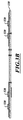
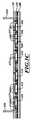
II.ハードウェア
図1Aおよび図1Bは、一例に係る、デバイスに組み込まれている多層電子機器アセンブリを示す簡略図である。図1Aは、デバイスの主なサブアセンブリを示す分解図である。サブアセンブリは、多層電子機器アセンブリ10、ベース基板20およびヒートシンク30を含む。
II. Hardware FIGS. 1A and 1B are simplified diagrams illustrating a multilayer electronics assembly incorporated into a device, according to an example. FIG. 1A is an exploded view showing the main subassemblies of the device. The subassembly includes a
本例において、ベース基板20は、窒化アルミニウム(AlN)製の銅直接接合(Direct Bonded Copper:DBC)基板であってよい。ベース基板20は、上面に配設される複数の導電配線22(例えば、銅配線等)、上面に接合されている複数のベアダイ24(例えば、パワー金属酸化膜半導体電界効果トランジスタMOSFET等)、および、上面から延在する複数の相互接続ポスト26を有する。
In this example, the
多層電子機器アセンブリ10は、内部に3次元方向にディスクリート電気回路素子が埋設されている。より詳細に後述するように、多層電子機器アセンブリ10は、ディスクリート電気回路素子が融着前にアセンブリの内部層に接合される融着プロセスによって形成される。複数の孔14は、基板20上のベアダイ24を収容するべく、多層電子機器アセンブリ10の底面に形成されている。図1Bに示すように、多層電子機器アセンブリ10はさらに、表面実装技術を利用して取着される高さのある部品を収容するべく上面に形成されている複数の孔16を備える。このように、能動型素子は多層電子機器アセンブリ10の上側である10b、または、多層電子機器アセンブリ10の下側である10aに取着することができる。
The multilayer
一例を挙げると、基板20上のベアダイ24は、ナノシルバー焼結技術を用いて多層電子機器アセンブリ10に取着される。例えば、孔14においてナノシルバー焼結ハンダペーストを用いるとしてよい。この例によると、ナノシルバー焼結は、約摂氏180度まで昇温してナノシルバーペースト中のバインダを焼成した後、温度を約摂氏280度まで昇温させて10分間にわたってナノシルバー粒子を焼結させるという温度プロフィールで実施する。結果として得られる界面「ハンダ」接合部は、従来の鉛ハンダまたは無鉛ハンダよりも耐熱性および電気抵抗が大幅に低く、繰り返される熱サイクルによって発生するストレスが存在する中でも品質が改善され、ハンダ接合部は摂氏900度を超えるまで「リフロー」しない。この最後の性質によって、多層電子機器アセンブリ10の融着プロセスに曝される可能性のある後処理、および、パワー半導体ハンダ接合部のリフローを実施することなく上側素子を処理後にハンダ付けすることが可能になる。
In one example, the
上述したように、多層電子機器アセンブリ10のディスクリート電気回路素子は、融着前にアセンブリの内部層に接合される。図2は、融着前の多層電子機器アセンブリの一例を示すより詳細な側面図である。
As described above, the discrete electrical circuit elements of the
アセンブリの底面から始めると、第1の層300はヒートシンクである。この例では、ヒートシンク300は、熱界面についてさまざまな選択肢をサポートするように成型され得る。例えば、導通のための実装孔310を持つ固体であったり、液体用の流路(不図示)、または、冷却用空気のためのピンフィン/スロット付きフィン(不図示)を備えたりする。
Starting from the bottom surface of the assembly, the
第2の層は、本例では両側に銅が形成されるベース層200である。ベース基板20と同様に、ベース層200は、窒化アルミニウム(AlN)製の銅直接接合(DBC)基板であってよい。ベース層200は、エポキシ、ハンダ(ナノシルバー焼結ハンダ、または、ヒートシンクが融着プロセス後に取着される場合は、標準的なハンダ)によって、または、ベース層200のヒートシンク側の面が銅で被覆されていない場合には、融着によって(別個に実施するか、または、アセンブリ全体について一回の処理として)、ヒートシンク300に取着されているとしてよい。複数のパワー半導体ダイ510、例えば、MOSFETは、回路レイアウトを最適化するべく、片側がベース層200に向いて下向きになるように配置される。より詳細に後述するが、これらの半導体ダイ510は、ナノシルバー焼結または過渡液相接合等のデバイス取着方法を利用して、ベース層200および多層電子機器アセンブリ100に取着するとしてよい。
The second layer is a
多層電子機器アセンブリ100は、ベース層200の上方に配置される。多層電子機器アセンブリ100の第1(最も下側)の層110は、スペーサとして、そして、半導体ダイ510の上側と下側との間の相互接続層として機能するとしてよい。複数の層120、130、140、150、160、170および180は、第1の層110の上方に積層される。これらの層は、ナノシルバー焼結または過渡液相接合等のデバイス取着方法を利用してディスクリート電子素子520、530および560が接合されているとしてよい。ディスクリート電子素子520は、例えば、受動型ディスクリート抵抗器、キャパシタ、磁気デバイスまたは能動型半導体デバイスであってよい。表面実装技術を利用してさらに素子540および550を上側に追加するとしてよい。デバイスは、例えば、電力をデバイスに供給する平坦な銅製の帯状インターコネクトである電力相互接続部600を含むとしてよい。
The multilayer
ガラスおよびセラミックで充填されているポリテトラフルオロエチレン(PTFE)等のフッ素重合体複合材の誘電特性は、無線周波数分野に適したパワーエレクトロニクスを含む多層構造を提供することに寄与する。しかし、上述したように、本開示の範囲は、基板材料としてPTFEを利用することに限定されない。 The dielectric properties of fluoropolymer composites such as polytetrafluoroethylene (PTFE) filled with glass and ceramic contribute to providing a multilayer structure including power electronics suitable for the radio frequency field. However, as described above, the scope of the present disclosure is not limited to using PTFE as a substrate material.
同様に、本開示は融着で形成されるアセンブリのみに限定されるものではない。例えば、エポキシファイバーグラス(FR4)またはポリアミド等を用いたプリントワイヤボード(PWB)材料で形成される層を利用することによって、3次元方向に埋設されたディスクリート電気回路素子を備える多層モジュールを形成することも可能である。層は、例えば、制御された接着剤、例えば、事前に樹脂マトリクスを含侵させた補強材料(「プリプレグ」)を用いて組み合わせることができるか、ナノシルバー焼結で直接組み合わせることができるか、過渡液相接合を利用して直接組み合わせることができるか、または、これらの方法を組み合わせるとしてよい。ナノシルバー焼結または過渡液相接合で直接組み合わせる場合、複数の層は処理中にガス放出させるために十分な間隙を設けるとしてよい。その後、環境暴露が懸念事項である場合、封止材を利用して層間の間隙を封止するとしてよい。 Similarly, the present disclosure is not limited to assemblies formed by fusion. For example, by using a layer formed of a printed wire board (PWB) material using epoxy fiber glass (FR4) or polyamide or the like, a multilayer module including discrete electric circuit elements embedded in a three-dimensional direction is formed. It is also possible. The layers can be combined, for example, using a controlled adhesive, eg, a reinforcing material previously impregnated with a resin matrix (“prepreg”), or can be combined directly with nanosilver sintering, They can be combined directly using transient liquid phase bonding or these methods may be combined. When combined directly with nanosilver sintering or transient liquid phase bonding, multiple layers may be provided with sufficient gaps to outgas during processing. Thereafter, when environmental exposure is a concern, the gap between the layers may be sealed using a sealing material.
ナノシルバー焼結または過渡液相接合によって、デバイスを各層に取着した後に、既に取着したデバイスが後でデバイスを取着するために必要な熱によって脱落してしまうことを懸念することなく、各層を順次焼結させることが可能になる。例えば、デバイス用の接合材料(ナノシルバー焼結または過渡液相接合の場合)は、デバイスを取着するための処理後に状態遷移が発生し、液体状態の流動性または柔軟性を持つ状態に戻るために処理後に大幅に高い温度が必要になる。この処理後の状態遷移温度も、最初にデバイスを取着するために必要な温度よりも大幅に高い。結果として得られる構造は、組み合わせ後に層に孔を形成することなく、多層モジュールにおいて3次元方向に埋設されているディスクリート電気回路素子を有する。 After attaching the device to each layer by nano silver sintering or transient liquid phase bonding, without worrying that the already attached device will fall off due to the heat required to attach the device later, Each layer can be sintered sequentially. For example, a bonding material for a device (in the case of nano silver sintering or transient liquid phase bonding) undergoes a state transition after processing to attach the device and returns to a liquid state fluidity or flexibility. Therefore, a significantly higher temperature is required after processing. The state transition temperature after this process is also significantly higher than the temperature required to initially attach the device. The resulting structure has discrete electrical circuit elements embedded in a three-dimensional direction in a multilayer module without forming holes in the layers after combination.
III.製造方法
多層モジュール内に3次元方向にディスクリート電気回路素子を埋設するための処理を図3Aから図3F、図4および図5を参照しつつ説明する。
III. Manufacturing Method A process for embedding a discrete electric circuit element in a three-dimensional direction in a multilayer module will be described with reference to FIGS. 3A to 3F, FIG. 4 and FIG.
図5に800と示す第1の処理において、多層電子機器アセンブリの各層を製造する。例えば、図3Aは層110および200を示す。層110は、ガラスおよびセラミックで充填されたフッ素重合体複合材(ポリテトラフルオロエチレン(PTFE)等)であってよい。ベース層200は、両面に形成された銅等の導体410を含む。上述したように、ベース層200は、AlNボードで形成される銅直接接合基板であってよい。ナノシルバー焼結を用いてデバイスを取着する層について、表面の最終的な仕上げは金または銀で行うとしてよい。図3Aに示すように、各層はビア420を含むとしてよい。ビア420によって、層同士を接続することが可能になる。
In a first process, indicated as 800 in FIG. 5, each layer of the multilayer electronics assembly is manufactured. For example, FIG. 3A shows
図5で810として示す第2の処理において、ディスクリート電気回路素子は各層に取着される。例えば、図3Bは、各層130に取着されている抵抗器およびキャパシタ等の受動型素子、または、小信号能動型デバイスであるディスクリート電気回路素子520を示す。ディスクリート電気回路素子520は、ナノシルバー焼結または過渡液相接合を用いて層130に接合されているとしてよい。過渡液相接合の一例は、「Highly Reliable Nickel−Tin Transient Liquid Phase Bonding Technology for High Temperature Operational Power Electronics in Electrified Vehicles」(Sang Won Yoon、Satoshi Yasuda、Michael D. Glover、Koji Shiozaki)に記載されている。ナノシルバー焼結の例は、国際公開公報第2005/079353号に記載されている。
In a second process, indicated as 810 in FIG. 5, discrete electrical circuit elements are attached to each layer. For example, FIG. 3B shows a
本例によると、ディスクリート電気回路素子520は、図4に示す温度プロフィールを利用して、ナノシルバー焼結によって各層130に取着されている。この例によると、10mm×10mmよりも小さい素子のダイ取着には圧力を用いていない。
According to this example, the discrete
図5に820と示す第3の処理によると、接合のためにサブアセンブリを組み立てる。例えば、図3Cは、ベース層200およびパワー半導体ダイ510と共に、層110および120から構成されるアセンブリを示す。相互接続ポスト430は、層の位置合わせを容易にする。この例では、ナノシルバーハンダペーストは、層110、120および200のそれぞれにシルクスクリーンで形成される。例えば、厚みが50μmのナノシルバーの層をシルクスクリーンで形成して、空気乾燥させる。この後、厚みが10μmのナノシルバーの層を塗布し、パワー半導体ダイ510を所定位置に配置し、層200、110および120を焼結プロセスのために配置する。層120には、通気孔122がパワー半導体ダイ510の上方および/または周囲に穿孔されている。これらの通気孔122によって、焼結プロセス中にナノシルバーハンダペースト中の溶媒およびバインダが放出される。
According to a third process, indicated as 820 in FIG. 5, the subassemblies are assembled for bonding. For example, FIG. 3C shows an assembly comprised of
続いて、図5に830として示すように、サブアセンブリの構成要素を互いに接合する。例えば、図3Dに図示しているように、プレート710および720に圧力を加える。プレート720には、層120内に形成されている通気孔122と位置合わせされている通気孔722が形成されている。圧力が加えられるのは、溶媒がダイの下方から焼成され、通気孔722によってガスが放出されるようにするためである。この例によると、10mm×10mmより大きいダイを利用する場合にナノシルバー焼結プロセスについて約3−5MPaを用いる。この例におけるプロフィールは実質的に、図4に図示したものと同じであるが、相違点として、圧力は摂氏180度で加えられ、当該プロフィールのうち10分間にわたって加えられる(そして、摂氏180度までの昇温中に必要に応じて/必要であれば加えられる)。摂氏275/300度に到達する前に圧力の印加を中止するとしてよい。
Subsequently, the components of the subassembly are joined together, as shown as 830 in FIG. For example, pressure is applied to
続いて、図5の840に示すように、融着のために複数の層を組み合わせる。例えば、図3Eに示すように、この時点において焼結で接合されている層110、120および200で構成されるサブアセンブリと共に、残りの層130、140、150、160、170および180を積層する。これらの層をこの後融着する(図5、850)。融着は通常、オートクレーブまたは液圧プレス内において基板層をPTFE複合材の融点を超える温度まで加熱しつつ、同時に決められた量の圧力を、好ましくは、機械的に、等方圧方式で、または、両方の組み合わせを利用して加えることで実行される。層の位置合わせは通常、複数のピン(本例における相互接続ポスト430等)を備える高精度固定具によって固定される。好ましくは、3個から8個であるが可能性としてそれ以上の個数を利用し、PTFE樹脂の状態が粘度の高い液体に変化する際に流動性を安定化させ、隣接する層が圧力を加えられることで融着する。接合している積層体のサイズに応じて、積層体の位置合わせ用のピン配置は、三角形状または矩形状が好ましい。ピン自体は、丸みを帯びているか、正方形状、矩形状、楕円形状またはひし形形状を持つことが好ましいが、他の形状であってもよい。
Subsequently, as shown at 840 in FIG. 5, a plurality of layers are combined for fusion. For example, as shown in FIG. 3E, the remaining
ディスクリート電気回路素子510、520および560がそれぞれの層にナノシルバー焼結または過渡液相接合によって取着されたので、ディスクリート電気回路素子510、520および560は、融着プロセス中もモジュール内の導電回路に接合された状態を維持することができる。例えば、過渡液相接合によって形成された合金の融点およびナノシルバー焼結によって形成された接合部の融点は、融着のためのPTFE複合材の融点に到達するために必要な温度をはるかに超えている。結果として得られる3次元の一体的な多層電子機器モジュール1000を図3Fに示す。多層電子機器モジュール1000では、複数のディスクリート電気回路素子510、520および560が、融着で形成されたブロック内に3次元方向に埋設されている。従来の融着で形成された多層モジュールとは異なり、図3Fのモジュール1000は、複数の層にディスクリート電気回路素子が積層されており、ディスクリート電気回路素子は垂直方向において重なっている。また、ディスクリート電気回路素子は、融着後にさらに穿孔処理およびメッキ処理を行うことなく、周囲の層に電気接続されている。さらに、湿気侵入は、融着によって形成された一体的な構造の一体性によって、防止されている。
Discrete
融着を実行した後、ヒートシンクおよび上側の表面実装素子を取着する(図5の860)。例えば、図3Fに示すように、ヒートシンク300は、多層電子機器モジュール1000の下方に取着され、上側の表面実装部品540および550は、多層電子機器モジュール1000の上面に取着されている。ベース層200のヒートシンク側が銅で被覆されていない場合、ヒートシンク300をベース層200に融着させることで低い耐熱性を実現し得る。一例を挙げると、これは、図3Eを参照しつつ説明した融着処理の一部として実現され得る。この場合、ヒートシンク300は、モジュール間を切断し易くするように、モジュール間に「ウェブ」マトリクスを含むように設計されているとしてよい。この切断処理は、ウォータージェット切断で実行するとしてよい。別の例を挙げると、ヒートシンク300は、Alスキンによって共に保持されている複数の部分モジュールにおいてAlSiC成型されるので、切断する必要があるのはAlスキンのみとしてよい。別の例を挙げると、ヒートシンク300は、図3Eに図示されているアセンブリにハンダ付けまたは接合されるとしてよい。
After performing the fusion, the heat sink and the upper surface mount element are attached (860 in FIG. 5). For example, as shown in FIG. 3F, the
上述したさまざまな実施形態を組み合わせて更なる実施形態を提供するとしてよい。本明細書で言及した米国特許、米国特許出願公開公報、米国特許出願、外国特許出願および非特許公開文献は全て、全内容を参照により本願に組み込む。実施形態の側面は、さらに異なる実施形態を提供するべくさまざまな特許、出願および公報の概念を利用するために必要であれば、修正するとしてよい。 The various embodiments described above may be combined to provide further embodiments. All U.S. patents, U.S. patent application publications, U.S. patent applications, foreign patent applications and non-patent publications mentioned herein are hereby incorporated by reference in their entirety. Aspects of the embodiments may be modified as necessary to utilize various patent, application and publication concepts to provide further different embodiments.
上記の詳細な説明を鑑みて実施形態について上記およびその他の変更を行うとしてよい。一般的に、以下に記載する特許請求の範囲では、利用している用語は特許請求の範囲を本明細書および特許請求の範囲に開示した具体的な実施形態に限定するものと解釈されるべきではなく、特許請求の範囲に対して認められる均等物の全範囲と共に全ての可能な実施形態を含むものと解釈すべきである。したがって、特許請求の範囲は開示によって限定されるものではない。なお、本明細書によれば、以下の各項目もまた実施形態として開示される。
[項目1]
積層された複数の基板層であって、前記複数の基板層のそれぞれが前記複数の基板層のうち少なくとも隣接する基板層に融着されている複数の基板層と、
前記複数の基板層のうち第1の基板層に接合されている第1のディスクリート電気回路素子と、
前記第1のディスクリート電気回路素子と前記第1の基板層との間に介在させている接合材料であって、前記接合材料が流動可能となるリフロー温度が前記複数の基板層の融着温度よりも高い接合材料と
を備える多層電子機器アセンブリ。
[項目2]
前記複数の基板層のうち第2の基板層に接合されている第2のディスクリート電気回路素子をさらに備える項目1に記載の多層電子機器アセンブリ。
[項目3]
前記複数の基板層は、第1の方向に積層されており、前記第1のディスクリート電気回路素子は、前記第1の方向において前記第2のディスクリート電気回路素子と重なっている項目2に記載の多層電子機器アセンブリ。
[項目4]
前記複数の基板層は、第1の方向に積層されており、前記第1のディスクリート電気回路素子は、積層された前記複数の基板層のうち複数の隣接する層の間に配置されている項目1から3の何れか1項に記載の多層電子機器アセンブリ。
[項目5]
前記複数の基板層は、フッ素重合体複合材を含む
項目1から4の何れか1項に記載の多層電子機器アセンブリ。
[項目6]
前記接合材料は、前記第1のディスクリート電気回路素子と前記第1の基板層とを接合するべく前記接合材料が流動可能となる初期フロー温度を持つ少なくとも一の材料で形成され、前記初期フロー温度は前記リフロー温度よりも低い項目1から5の何れか1項に記載の多層電子機器アセンブリ。
[項目7]
前記接合材料は、前記リフロー温度に到達する直前は固体である項目1から6の何れか1項に記載の多層電子機器アセンブリ。
[項目8]
前記接合材料は、ナノシルバー焼結ハンダである項目1から7の何れか1項に記載の多層電子機器アセンブリ。
[項目9]
前記接合材料は、過渡液相接合合金である項目1から7の何れか1項記載の多層電子機器アセンブリ。
[項目10]
前記第1のディスクリート電気回路素子は、受動型ディスクリート抵抗器、キャパシタ、磁気デバイスおよび能動型半導体デバイスのうち1つである項目1から9の何れか1項に記載の多層電子機器アセンブリ。
[項目11]
融点が第1の温度である第1の材料で形成される3次元単一ブロックと、
前記3次元単一ブロックに埋設されている複数のディスクリート電気回路素子と
を備え、
前記複数のディスクリート電気回路素子のそれぞれは、第2の材料によって前記3次元単一ブロックに接合されており、前記第2の材料は、前記第2の材料が流動可能となるリフロー温度が、前記第1の温度より高い第2の温度である多層電子機器モジュール。
[項目12]
前記3次元単一ブロックは、上面、底面および複数の側面によって画定されている外部表面を含み、
前記第1の材料は、前記複数のディスクリート電気回路素子のうち少なくとも第1のディスクリート電気回路素子を完全に取り囲み、前記第1の材料が、前記複数のディスクリート電気回路素子のうち前記第1のディスクリート電気回路素子の全ての側面と、前記3次元単一ブロックの前記外部表面上の任意の点との間に配置される項目11に記載の多層電子機器モジュール。
[項目13]
前記第1の材料は、前記複数のディスクリート電気回路素子のうち前記第1のディスクリート電気回路素子と直接接触していない項目12に記載の多層電子機器モジュール。
[項目14]
前記複数のディスクリート電気回路素子は、第1のディスクリート電気回路素子、第2のディスクリート電気回路素子、および、第3のディスクリート電気回路素子を含み、前記第1のディスクリート電気回路素子は、第1の方向において前記第2のディスクリート電気回路素子と重なっており、前記第1のディスクリート電気回路素子は、前記第1の方向と垂直な第2の方向において、前記第3のディスクリート電気回路素子と重なっている項目11から13の何れか1項に記載の多層電子機器モジュール。
[項目15]
前記第1の材料は、フッ素重合体複合材である項目11から14の何れか1項に記載の多層電子機器モジュール。
[項目16]
前記第2の材料は、前記複数のディスクリート電気回路素子と第1の層とを接合するべく、前記第2の材料が流動可能となる初期フロー温度を持つ少なくとも1つの材料で形成されており、前記初期フロー温度は、前記第2の温度よりも低い項目11から15の何れか1項に記載の多層電子機器モジュール。
[項目17]
前記第2の材料は、前記第2の温度に到達する直前は固体である項目11から16の何れか1項に記載の多層電子機器モジュール。
[項目18]
前記第2の材料はナノシルバー焼結ハンダである項目11から17の何れか1項に記載の多層電子機器モジュール。
[項目19]
前記第1の材料は、過渡液相接合合金である項目11から17の何れか1項に記載の多層電子機器モジュール。
[項目20]
前記複数のディスクリート電気回路素子は、受動型ディスクリート抵抗器、キャパシタ、磁気デバイスおよび能動型半導体デバイスから成る群から選択される
項目11から19の何れか1項に記載の多層電子機器モジュール。
[項目21]
パワー半導体ダイが接合されている一次基板と、
前記一次基板上に積層されており、互いに融着されている複数の二次基板と、
前記複数の二次基板のうち、前記一次基板から最も離れた位置にある二次基板の外部表面に取着されている能動型電子素子と
を備え、
第1のディスクリート電気回路素子は、前記複数の二次基板の融着温度よりも高い第1の融点を持つ第1の材料で、前記複数の二次基板のうち第1の基板に接合されており、
第2のディスクリート電気回路素子は、前記複数の二次基板の前記融着温度よりも高い第2の融点を持つ第2の材料で前記複数の二次基板のうち第2の基板に接合されている多機能モジュール。
[項目22]
前記第1の材料は、前記第2の材料と同じである項目21に記載の多機能モジュール。
[項目23]
多層モジュール内に複数のディスクリート電気回路素子を埋設する方法であって、
最初は第1の温度において流動可能である第1の接合材料を用いて第1のディスクリート電気回路素子を第1の基板に取着する段階であって、前記第1の接合材料において状態遷移を発生させ、前記第1の接合材料が硬化すると、前記第1の接合材料は、前記第1の温度よりも高い第2の温度に到達するまでは流動可能状態には戻らない段階と、
前記第1の接合材料を用いて第2のディスクリート電気回路素子を第2の基板に取着する段階と、
前記第1の基板を前記第2の基板に融着する段階と
を備え、
前記第1の温度は、前記第1の基板の融着温度よりも低く、前記第2の温度は、前記第1の基板の前記融着温度よりも高い
多層モジュール内に複数のディスクリート電気回路素子を埋設する方法。
[項目24]
前記第1のディスクリート電気回路素子を前記第1の基板に取着する段階は、前記第1のディスクリート電気回路素子を前記第1の基板にナノシルバー焼結する段階を有する項目22に記載の多層モジュール内に複数のディスクリート電気回路素子を埋設する方法。
[項目25]
前記第1のディスクリート電気回路素子を前記第1の基板に取着する段階は、前記第1のディスクリート電気回路素子を前記第1の基板に過渡液相接合する段階を有する項目22に記載の多層モジュール内に複数のディスクリート電気回路素子を埋設する方法。
[項目26]
第1の方向に積層されている複数の基板層であって、前記複数の基板層のそれぞれは、前記複数の基板層のうち少なくとも隣接する基板層に接合されている複数の基板層と、
接合材料であって、前記接合材料が最初に流動可能となる初期転移温度と、前記接合材料が、最初に流動可能となった後に硬化した後に流動可能となる後続転移温度を持つ接合材料と、
前記接合材料を用いて前記複数の基板層のうち第1の基板層に接合されている第1のディスクリート電気回路素子と、
前記接合材料を用いて前記複数の基板層のうち第2の基板層に接合されている第2のディスクリート電気回路素子と
を備え、
前記初期転移温度は前記後続転移温度よりも低く、
前記第2のディスクリート電気回路素子は、前記第1の方向において前記第1のディスクリート電気回路素子と重なっている
多層電子機器アセンブリ。
[項目27]
前記接合材料は、前記後続転移温度に到達する直前は固体である項目26に記載の多層電子機器アセンブリ。
[項目28]
前記複数の基板層は、エポキシファイバーグラスおよびポリアミドのうち少なくとも一方を含む項目26または27に記載の多層電子機器アセンブリ。
[項目29]
前記接合材料は、ナノシルバー焼結ハンダである項目26から28の何れか1項に記載の多層電子機器アセンブリ。
[項目30]
前記接合材料は、過渡液相接合合金である項目26から28の何れか1項に記載の多層電子機器アセンブリ。
[項目31]
前記第1のディスクリート電気回路素子は、受動型ディスクリート抵抗器、キャパシタ、磁気デバイスおよび能動型半導体デバイスのうちの1つである項目26から30の何れか1項に記載の多層電子機器アセンブリ。
[項目32]
多層モジュール内に複数のディスクリート電気回路素子を埋設する方法であって、
最初は第1の温度において流動可能である接合材料を用いて第1のディスクリート電気回路素子を第1の基板に取着する段階であって、前記接合材料において状態遷移を発生させることで、前記接合材料が硬化した後、前記接合材料は、前記第1の温度よりも高い第2の温度に到達するまでは流動可能状態には戻らないようにする段階と、
第2の基板を前記第1の基板に取着する段階と、
前記第1の温度において前記接合材料を用いて第2のディスクリート電気回路素子を前記第2の基板に取着する段階と
を備える多層モジュール内に複数のディスクリート電気回路素子を埋設する方法。
The above and other changes may be made to the embodiments in light of the above detailed description. Generally, in the claims set forth below, the terms utilized should be construed as limiting the claims to the specific embodiments disclosed in the specification and the claims. Rather, it should be construed as including all possible embodiments with the full scope of equivalents to which the claims are entitled. Accordingly, the claims are not limited by the disclosure. According to the present specification, the following items are also disclosed as embodiments.
[Item 1]
A plurality of laminated substrate layers, each of the plurality of substrate layers being fused to at least an adjacent substrate layer of the plurality of substrate layers;
A first discrete electrical circuit element bonded to a first substrate layer of the plurality of substrate layers;
A bonding material interposed between the first discrete electric circuit element and the first substrate layer, wherein a reflow temperature at which the bonding material can flow is higher than a fusion temperature of the plurality of substrate layers. Even with high bonding materials
A multilayer electronics assembly comprising:
[Item 2]
The multilayer electronic device assembly according to item 1, further comprising a second discrete electric circuit element bonded to a second substrate layer of the plurality of substrate layers.
[Item 3]
The plurality of substrate layers are stacked in a first direction, and the first discrete electric circuit element overlaps the second discrete electric circuit element in the first direction. Multi-layer electronics assembly.
[Item 4]
The plurality of substrate layers are stacked in a first direction, and the first discrete electric circuit element is disposed between a plurality of adjacent layers among the plurality of stacked substrate layers. 4. The multilayer electronic device assembly according to any one of 1 to 3.
[Item 5]
The plurality of substrate layers include a fluoropolymer composite material
Item 5. The multilayer electronic device assembly according to any one of Items 1 to 4.
[Item 6]
The bonding material is formed of at least one material having an initial flow temperature at which the bonding material can flow to bond the first discrete electric circuit element and the first substrate layer, and the initial flow temperature. The multilayer electronic device assembly according to any one of items 1 to 5, wherein is lower than the reflow temperature.
[Item 7]
The multilayer electronic device assembly according to any one of items 1 to 6, wherein the bonding material is solid immediately before reaching the reflow temperature.
[Item 8]
The multilayer electronic device assembly according to any one of items 1 to 7, wherein the bonding material is nano silver sintered solder.
[Item 9]
The multilayer electronic device assembly according to any one of items 1 to 7, wherein the bonding material is a transient liquid phase bonding alloy.
[Item 10]
10. The multilayer electronic device assembly according to any one of items 1 to 9, wherein the first discrete electric circuit element is one of a passive discrete resistor, a capacitor, a magnetic device, and an active semiconductor device.
[Item 11]
A three-dimensional single block formed of a first material having a melting point of a first temperature;
A plurality of discrete electric circuit elements embedded in the three-dimensional single block;
With
Each of the plurality of discrete electric circuit elements is joined to the three-dimensional single block by a second material, and the second material has a reflow temperature at which the second material can flow, A multilayer electronic device module having a second temperature higher than the first temperature.
[Item 12]
The three-dimensional single block includes an outer surface defined by a top surface, a bottom surface and a plurality of side surfaces;
The first material completely surrounds at least a first discrete electrical circuit element of the plurality of discrete electrical circuit elements, and the first material is the first discrete electrical circuit element of the plurality of discrete electrical circuit elements. 12. The multilayer electronic device module according to item 11, which is disposed between all side surfaces of the electric circuit element and an arbitrary point on the outer surface of the three-dimensional single block.
[Item 13]
13. The multilayer electronic device module according to item 12, wherein the first material is not in direct contact with the first discrete electric circuit element among the plurality of discrete electric circuit elements.
[Item 14]
The plurality of discrete electrical circuit elements include a first discrete electrical circuit element, a second discrete electrical circuit element, and a third discrete electrical circuit element, wherein the first discrete electrical circuit element includes a first discrete electrical circuit element, The first discrete electrical circuit element overlaps the third discrete electrical circuit element in a second direction perpendicular to the first direction. 14. The multilayer electronic device module according to any one of items 11 to 13.
[Item 15]
15. The multilayer electronic device module according to any one of items 11 to 14, wherein the first material is a fluoropolymer composite material.
[Item 16]
The second material is formed of at least one material having an initial flow temperature at which the second material can flow in order to join the plurality of discrete electric circuit elements and the first layer; The multilayer electronic device module according to any one of items 11 to 15, wherein the initial flow temperature is lower than the second temperature.
[Item 17]
The multilayer electronic device module according to any one of items 11 to 16, wherein the second material is a solid immediately before reaching the second temperature.
[Item 18]
18. The multilayer electronic device module according to any one of items 11 to 17, wherein the second material is nano silver sintered solder.
[Item 19]
18. The multilayer electronic device module according to any one of items 11 to 17, wherein the first material is a transient liquid phase bonding alloy.
[Item 20]
The plurality of discrete electrical circuit elements are selected from the group consisting of passive discrete resistors, capacitors, magnetic devices, and active semiconductor devices.
20. The multilayer electronic device module according to any one of items 11 to 19.
[Item 21]
A primary substrate to which a power semiconductor die is bonded;
A plurality of secondary substrates laminated on the primary substrate and fused together;
An active electronic element attached to the outer surface of the secondary substrate located farthest from the primary substrate among the plurality of secondary substrates;
With
The first discrete electric circuit element is a first material having a first melting point higher than a fusion temperature of the plurality of secondary substrates, and is bonded to the first substrate among the plurality of secondary substrates. And
The second discrete electric circuit element is bonded to a second substrate of the plurality of secondary substrates with a second material having a second melting point higher than the fusion temperature of the plurality of secondary substrates. Multi-function module.
[Item 22]
The multifunction module according to item 21, wherein the first material is the same as the second material.
[Item 23]
A method of embedding a plurality of discrete electric circuit elements in a multilayer module,
Initially, a first discrete electrical circuit element is attached to a first substrate using a first bonding material that is flowable at a first temperature, wherein a state transition is performed in the first bonding material. Generating and curing of the first bonding material, the first bonding material does not return to a flowable state until a second temperature higher than the first temperature is reached;
Attaching a second discrete electrical circuit element to a second substrate using the first bonding material;
Fusing the first substrate to the second substrate;
With
The first temperature is lower than the fusing temperature of the first substrate, and the second temperature is higher than the fusing temperature of the first substrate.
A method of embedding a plurality of discrete electric circuit elements in a multilayer module.
[Item 24]
The multilayer of
[Item 25]
24. The multilayer of
[Item 26]
A plurality of substrate layers stacked in a first direction, wherein each of the plurality of substrate layers is bonded to at least an adjacent substrate layer of the plurality of substrate layers;
A bonding material having an initial transition temperature at which the bonding material is initially flowable and a subsequent transition temperature at which the bonding material is flowable after being cured after first being flowable;
A first discrete electric circuit element bonded to a first substrate layer of the plurality of substrate layers using the bonding material;
A second discrete electric circuit element bonded to a second substrate layer of the plurality of substrate layers using the bonding material;
With
The initial transition temperature is lower than the subsequent transition temperature;
The second discrete electrical circuit element overlaps the first discrete electrical circuit element in the first direction.
Multi-layer electronics assembly.
[Item 27]
27. The multilayer electronic assembly of
[Item 28]
28. The multilayer electronic device assembly according to
[Item 29]
29. The multilayer electronic device assembly according to any one of
[Item 30]
29. The multilayer electronic device assembly according to any one of
[Item 31]
31. The multilayer electronic assembly of any of items 26-30, wherein the first discrete electrical circuit element is one of a passive discrete resistor, a capacitor, a magnetic device, and an active semiconductor device.
[Item 32]
A method of embedding a plurality of discrete electric circuit elements in a multilayer module,
First, attaching a first discrete electrical circuit element to a first substrate using a bonding material that is flowable at a first temperature, wherein a state transition is generated in the bonding material, After the bonding material has hardened, the bonding material does not return to a flowable state until a second temperature higher than the first temperature is reached;
Attaching a second substrate to the first substrate;
Attaching a second discrete electrical circuit element to the second substrate using the bonding material at the first temperature;
A method of embedding a plurality of discrete electric circuit elements in a multilayer module comprising:
Claims (9)
最初は第1の温度において流動可能である第1の接合材料を用いて第1のディスクリート電気回路素子を第1の基板に取着する段階であって、前記第1の接合材料において状態遷移を発生させ、前記第1の接合材料が硬化すると、前記第1の接合材料は、前記第1の温度よりも高い第2の温度に到達するまでは流動可能状態には戻らない段階と、
前記第1の接合材料を用いて第2のディスクリート電気回路素子を第2の基板に取着する段階と、
前記第1の基板を前記第2の基板に融着する段階と
を備え、
前記第1の温度は、前記第1の基板の融着温度よりも低く、前記第2の温度は、前記第1の基板の前記融着温度よりも高い
多層モジュール内に複数のディスクリート電気回路素子を埋設する方法。 A method of embedding a plurality of discrete electric circuit elements in a multilayer module,
Initially, a first discrete electrical circuit element is attached to a first substrate using a first bonding material that is flowable at a first temperature, wherein a state transition is performed in the first bonding material. Generating and curing of the first bonding material, the first bonding material does not return to a flowable state until a second temperature higher than the first temperature is reached;
Attaching a second discrete electrical circuit element to a second substrate using the first bonding material;
Fusing the first substrate to the second substrate, and
The first temperature is lower than the fusing temperature of the first substrate, and the second temperature is higher than the fusing temperature of the first substrate. A plurality of discrete electric circuit elements in a multilayer module How to bury.
接合材料であって、前記接合材料が最初に流動可能となる初期転移温度と、前記接合材料が、最初に流動可能となった後に硬化した後に流動可能となる後続転移温度を持つ接合材料と、
前記接合材料を用いて前記複数の基板層のうち第1の基板層に接合されている第1のディスクリート電気回路素子と、
前記接合材料を用いて前記複数の基板層のうち第2の基板層に接合されている第2のディスクリート電気回路素子と
を備え、
前記初期転移温度は前記後続転移温度よりも低く、前記融着の際の前記複数の基板層の融点は前記後続転移温度よりも低く、
前記第2のディスクリート電気回路素子は、前記第1の方向において前記第1のディスクリート電気回路素子と重なっている
多層電子機器アセンブリ。 A plurality of substrate layers laminated in a first direction, wherein each of the plurality of substrate layers is bonded to at least an adjacent substrate layer among the plurality of substrate layers by fusion bonding. When,
A bonding material having an initial transition temperature at which the bonding material is initially flowable and a subsequent transition temperature at which the bonding material is flowable after being cured after first being flowable;
A first discrete electric circuit element bonded to a first substrate layer of the plurality of substrate layers using the bonding material;
A second discrete electric circuit element bonded to a second substrate layer among the plurality of substrate layers using the bonding material;
The initial transition temperature is lower than the subsequent transition temperature , and the melting points of the plurality of substrate layers during the fusion are lower than the subsequent transition temperature;
The second discrete electrical circuit element overlaps the first discrete electrical circuit element in the first direction.
Applications Claiming Priority (5)
| Application Number | Priority Date | Filing Date | Title |
|---|---|---|---|
| US201261596652P | 2012-02-08 | 2012-02-08 | |
| US61/596,652 | 2012-02-08 | ||
| US13/758,843 US9888568B2 (en) | 2012-02-08 | 2013-02-04 | Multilayer electronics assembly and method for embedding electrical circuit components within a three dimensional module |
| US13/758,843 | 2013-02-04 | ||
| PCT/US2013/024907 WO2013119643A1 (en) | 2012-02-08 | 2013-02-06 | Multilayer electronics assembly and method for embedding electrical circuit components within a three dimensional module |
Publications (2)
| Publication Number | Publication Date |
|---|---|
| JP2015508235A JP2015508235A (en) | 2015-03-16 |
| JP6257047B2 true JP6257047B2 (en) | 2018-01-10 |
Family
ID=48902707
Family Applications (1)
| Application Number | Title | Priority Date | Filing Date |
|---|---|---|---|
| JP2014556629A Active JP6257047B2 (en) | 2012-02-08 | 2013-02-06 | Multilayer electronic device assembly and method for embedding electrical circuit elements in a three-dimensional module |
Country Status (5)
| Country | Link |
|---|---|
| US (2) | US9888568B2 (en) |
| JP (1) | JP6257047B2 (en) |
| KR (1) | KR102103196B1 (en) |
| HK (2) | HK1203739A1 (en) |
| IN (1) | IN2014DN07180A (en) |
Families Citing this family (24)
| Publication number | Priority date | Publication date | Assignee | Title |
|---|---|---|---|---|
| US9044822B2 (en) * | 2012-04-17 | 2015-06-02 | Toyota Motor Engineering & Manufacturing North America, Inc. | Transient liquid phase bonding process for double sided power modules |
| JP6072667B2 (en) * | 2013-11-12 | 2017-02-01 | 三菱電機株式会社 | Semiconductor module and manufacturing method thereof |
| US9607964B2 (en) * | 2014-03-28 | 2017-03-28 | Intel Corporation | Method and materials for warpage thermal and interconnect solutions |
| DE102014206601A1 (en) | 2014-04-04 | 2015-10-08 | Siemens Aktiengesellschaft | A method of mounting an electrical component using a hood and a hood suitable for use in this method |
| DE102014206606A1 (en) | 2014-04-04 | 2015-10-08 | Siemens Aktiengesellschaft | Method for mounting an electrical component on a substrate |
| DE102014206608A1 (en) | 2014-04-04 | 2015-10-08 | Siemens Aktiengesellschaft | A method of mounting an electrical component using a hood and a hood suitable for use in this method |
| US9831768B2 (en) | 2014-07-17 | 2017-11-28 | Crane Electronics, Inc. | Dynamic maneuvering configuration for multiple control modes in a unified servo system |
| US9230726B1 (en) | 2015-02-20 | 2016-01-05 | Crane Electronics, Inc. | Transformer-based power converters with 3D printed microchannel heat sink |
| US9589864B2 (en) * | 2015-05-14 | 2017-03-07 | Qorvo Us, Inc. | Substrate with embedded sintered heat spreader and process for making the same |
| KR102490164B1 (en) * | 2015-12-31 | 2023-01-18 | 엘지디스플레이 주식회사 | White organic light emitting diode display device |
| US9780635B1 (en) | 2016-06-10 | 2017-10-03 | Crane Electronics, Inc. | Dynamic sharing average current mode control for active-reset and self-driven synchronous rectification for power converters |
| FR3059466B1 (en) * | 2016-11-30 | 2019-07-05 | Sagemcom Broadband Sas | HEAT EXHAUST DEVICE |
| US9742183B1 (en) | 2016-12-09 | 2017-08-22 | Crane Electronics, Inc. | Proactively operational over-voltage protection circuit |
| US9735566B1 (en) | 2016-12-12 | 2017-08-15 | Crane Electronics, Inc. | Proactively operational over-voltage protection circuit |
| US11524359B2 (en) | 2017-08-23 | 2022-12-13 | Georgia Tech Research Corporation | Low temperature direct bonding of aluminum nitride to AlSiC substrates |
| US9979285B1 (en) | 2017-10-17 | 2018-05-22 | Crane Electronics, Inc. | Radiation tolerant, analog latch peak current mode control for power converters |
| US10425080B1 (en) | 2018-11-06 | 2019-09-24 | Crane Electronics, Inc. | Magnetic peak current mode control for radiation tolerant active driven synchronous power converters |
| GB201917680D0 (en) * | 2019-12-04 | 2020-01-15 | Sinclair Grant | Wafr v1 |
| US11626340B2 (en) | 2019-12-12 | 2023-04-11 | Qorvo Us, Inc. | Integrated circuit (IC) package with embedded heat spreader in a redistribution layer (RDL) |
| EP3840548A1 (en) * | 2019-12-20 | 2021-06-23 | AT & S Austria Technologie & Systemtechnik Aktiengesellschaft | Component carrier and method of manufacturing the same |
| CN111799251B (en) * | 2020-07-09 | 2023-06-02 | 华羿微电子股份有限公司 | Power discrete device adopting multi-chip stacking structure and preparation method thereof |
| US11497112B2 (en) * | 2020-12-11 | 2022-11-08 | Toyota Motor Engineering & Manufacturing North America, Inc. | Driver board assemblies and methods of forming a driver board assembly |
| CN116529734A (en) * | 2021-01-14 | 2023-08-01 | 凸版印刷株式会社 | Card medium and method for manufacturing card medium |
| TWI796738B (en) * | 2021-07-23 | 2023-03-21 | 先豐通訊股份有限公司 | Circuit board structure having waveguide and method for manufacturing the same |
Family Cites Families (171)
| Publication number | Priority date | Publication date | Assignee | Title |
|---|---|---|---|---|
| US3144627A (en) | 1960-07-05 | 1964-08-11 | Weldex Division Of Metal Craft | Welding transformer with colled core |
| US3201728A (en) | 1962-08-23 | 1965-08-17 | Westinghouse Electric Corp | Evaporative cooled inductive apparatus having cast solid insulation with cooling ducts formed therein |
| US3761843A (en) | 1972-05-16 | 1973-09-25 | Merrimac Ind Inc | Four port networks synthesized from interconnection of coupled and uncoupled sections of line lengths |
| US4342143A (en) | 1974-02-04 | 1982-08-03 | Jennings Thomas A | Method of making multiple electrical components in integrated microminiature form |
| US3949327A (en) | 1974-08-01 | 1976-04-06 | Sage Laboratories, Inc. | Waveguide low pass filter |
| US3955161A (en) | 1974-08-05 | 1976-05-04 | General Dynamics Corporation | Molded waveguide filter with integral tuning posts |
| US3999150A (en) | 1974-12-23 | 1976-12-21 | International Business Machines Corporation | Miniaturized strip-line directional coupler package having spirally wound coupling lines |
| US4337569A (en) | 1978-02-27 | 1982-07-06 | General Electric Company | Method of making integrally formed transformer cooling ducts |
| US4430758A (en) | 1982-06-03 | 1984-02-07 | Scientific Component Corporation | Suspended-substrate co-planar stripline mixer |
| JPS5986307A (en) | 1982-11-09 | 1984-05-18 | Shimada Phys & Chem Ind Co Ltd | Evanescent mode type resonator |
| CA1194159A (en) | 1984-05-28 | 1985-09-24 | Abdelmegid K. Saad | Low pass filters with finite transmission zeros in evanescent modes |
| IT1183558B (en) | 1985-04-02 | 1987-10-22 | Gte Telecom Spa | THIN FILM POWER COUPLER |
| JPS63170780A (en) | 1986-10-03 | 1988-07-14 | インタランド・コーポレーション | Integrated multi-display type overlay control system communication work station |
| JPS63220603A (en) | 1987-03-10 | 1988-09-13 | Yuniden Kk | Ceramic waveguide filtering circuit |
| US4800345A (en) | 1988-02-09 | 1989-01-24 | Pacific Monolithics | Spiral hybrid coupler |
| FR2632123B1 (en) | 1988-05-27 | 1991-01-18 | Alcatel Thomson Faisceaux | MULTIPLEX MICROWAVE FILTER, AND METHOD FOR ADJUSTING SUCH A FILTER |
| US4837535A (en) | 1989-01-05 | 1989-06-06 | Uniden Corporation | Resonant wave filter |
| US4956626A (en) | 1989-01-13 | 1990-09-11 | Sundstrand Corporation | Inductor transformer cooling apparatus |
| US5053921A (en) | 1989-05-15 | 1991-10-01 | Rogers Corporation | Multilayer interconnect device and method of manufacture thereof |
| JPH0344067A (en) | 1989-07-11 | 1991-02-25 | Nec Corp | Laminating method of semiconductor substrate |
| US5799320A (en) | 1989-08-23 | 1998-08-25 | John R. Klug | Remote multiple-user editing system and method |
| GB2239142A (en) | 1989-12-15 | 1991-06-19 | Philips Electronic Associated | Variable bi-phase modulator circuits and variable resistors |
| US5032803A (en) | 1990-02-02 | 1991-07-16 | American Telephone & Telegraph Company | Directional stripline structure and manufacture |
| US5046238A (en) * | 1990-03-15 | 1991-09-10 | Rogers Corporation | Method of manufacturing a multilayer circuit board |
| US5227338A (en) | 1990-04-30 | 1993-07-13 | International Business Machines Corporation | Three-dimensional memory card structure with internal direct chip attachment |
| US5099309A (en) | 1990-04-30 | 1992-03-24 | International Business Machines Corporation | Three-dimensional memory card structure with internal direct chip attachment |
| US5073814A (en) | 1990-07-02 | 1991-12-17 | General Electric Company | Multi-sublayer dielectric layers |
| US5065122A (en) | 1990-09-04 | 1991-11-12 | Motorola, Inc. | Transmission line using fluroplastic as a dielectric |
| US5598327A (en) | 1990-11-30 | 1997-01-28 | Burr-Brown Corporation | Planar transformer assembly including non-overlapping primary and secondary windings surrounding a common magnetic flux path area |
| JP3016292B2 (en) | 1991-11-20 | 2000-03-06 | 日本電気株式会社 | Polyimide multilayer wiring board and method of manufacturing the same |
| FR2675632B1 (en) | 1991-04-18 | 1997-04-30 | Texas Instruments France | INTEGRATED CIRCUIT CONDITIONING DEVICE |
| US5293619A (en) | 1991-05-30 | 1994-03-08 | Sandia Corporation | Method and apparatus for collaborative use of application program |
| CA2071662A1 (en) | 1991-06-26 | 1992-12-27 | Jon J. Gulick | Integrated socket-type package for flip-chip semiconductor devices and circuits |
| JP2817487B2 (en) | 1991-12-09 | 1998-10-30 | 株式会社村田製作所 | Chip type directional coupler |
| JP2840493B2 (en) | 1991-12-27 | 1998-12-24 | 株式会社日立製作所 | Integrated microwave circuit |
| US5287619A (en) | 1992-03-09 | 1994-02-22 | Rogers Corporation | Method of manufacture multichip module substrate |
| US5440805A (en) | 1992-03-09 | 1995-08-15 | Rogers Corporation | Method of manufacturing a multilayer circuit |
| US5526517A (en) | 1992-05-15 | 1996-06-11 | Lsi Logic Corporation | Concurrently operating design tools in an electronic computer aided design system |
| US5309629A (en) | 1992-09-01 | 1994-05-10 | Rogers Corporation | Method of manufacturing a multilayer circuit board |
| US5274912A (en) | 1992-09-01 | 1994-01-04 | Rogers Corporation | Method of manufacturing a multilayer circuit board |
| US5329695A (en) * | 1992-09-01 | 1994-07-19 | Rogers Corporation | Method of manufacturing a multilayer circuit board |
| GB2272312A (en) | 1992-11-10 | 1994-05-11 | Ibm | Collaborative working in a network. |
| US5406234A (en) | 1992-12-30 | 1995-04-11 | Itt Corporation | Tunable microwave filter apparatus having a notch resonator |
| US5306670A (en) * | 1993-02-09 | 1994-04-26 | Texas Instruments Incorporated | Multi-chip integrated circuit module and method for fabrication thereof |
| US5446842A (en) | 1993-02-26 | 1995-08-29 | Taligent, Inc. | Object-oriented collaboration system |
| EP0622930A3 (en) | 1993-03-19 | 1996-06-05 | At & T Global Inf Solution | Application sharing for computer collaboration system. |
| US5704042A (en) | 1993-03-19 | 1997-12-30 | Ncr Corporation | Accelerated replication of multiple computer displays |
| US5608872A (en) | 1993-03-19 | 1997-03-04 | Ncr Corporation | System for allowing all remote computers to perform annotation on an image and replicating the annotated image on the respective displays of other comuters |
| US5649104A (en) | 1993-03-19 | 1997-07-15 | Ncr Corporation | System for allowing user of any computer to draw image over that generated by the host computer and replicating the drawn image to other computers |
| JP3198796B2 (en) | 1993-06-25 | 2001-08-13 | 富士電機株式会社 | Mold module |
| JP2656000B2 (en) | 1993-08-31 | 1997-09-24 | 日立金属株式会社 | Stripline type high frequency components |
| US5689641A (en) | 1993-10-01 | 1997-11-18 | Vicor, Inc. | Multimedia collaboration system arrangement for routing compressed AV signal through a participant site without decompressing the AV signal |
| US5428840A (en) | 1993-12-10 | 1995-06-27 | Itt Corporation | Monolithic double balanced microstrip mixer with flat conversion loss |
| US5382931A (en) | 1993-12-22 | 1995-01-17 | Westinghouse Electric Corporation | Waveguide filters having a layered dielectric structure |
| US5499005A (en) | 1994-01-28 | 1996-03-12 | Gu; Wang-Chang A. | Transmission line device using stacked conductive layers |
| US5467064A (en) | 1994-01-28 | 1995-11-14 | Motorola, Inc. | Embedded ground plane for providing shielded layers in low volume multilayer transmission line devices |
| EP0763868B1 (en) | 1994-05-19 | 2004-02-18 | TDK Corporation | Directional coupler |
| US5469124A (en) | 1994-06-10 | 1995-11-21 | Westinghouse Electric Corp. | Heat dissipating transformer coil |
| JPH0816514A (en) | 1994-07-01 | 1996-01-19 | Hitachi Ltd | Coopperation support system |
| JPH0845738A (en) | 1994-07-27 | 1996-02-16 | Canon Inc | Inductance element |
| US5604490A (en) | 1994-09-09 | 1997-02-18 | International Business Machines Corporation | Method and system for providing a user access to multiple secured subsystems |
| US5579207A (en) * | 1994-10-20 | 1996-11-26 | Hughes Electronics | Three-dimensional integrated circuit stacking |
| EP1463264A3 (en) | 1994-12-01 | 2005-11-23 | Sharp Kabushiki Kaisha | Communication equipment |
| US5495394A (en) | 1994-12-19 | 1996-02-27 | At&T Global Information Solutions Company | Three dimensional die packaging in multi-chip modules |
| US5745017A (en) | 1995-01-03 | 1998-04-28 | Rf Prime Corporation | Thick film construct for quadrature translation of RF signals |
| US5534830A (en) | 1995-01-03 | 1996-07-09 | R F Prime Corporation | Thick film balanced line structure, and microwave baluns, resonators, mixers, splitters, and filters constructed therefrom |
| US5887170A (en) | 1995-02-13 | 1999-03-23 | International Business Machines Corporation | System for classifying and sending selective requests to different participants of a collaborative application thereby allowing concurrent execution of collaborative and non-collaborative applications |
| US5724508A (en) | 1995-03-09 | 1998-03-03 | Insoft, Inc. | Apparatus for collaborative computing |
| US5576669A (en) | 1995-04-28 | 1996-11-19 | Motorola, Inc. | Multi-layered bi-directional coupler |
| US5657537A (en) | 1995-05-30 | 1997-08-19 | General Electric Company | Method for fabricating a stack of two dimensional circuit modules |
| US5974335A (en) | 1995-06-07 | 1999-10-26 | Northrop Grumman Corporation | High-temperature superconducting microwave delay line of spiral configuration |
| US5629241A (en) | 1995-07-07 | 1997-05-13 | Hughes Aircraft Company | Microwave/millimeter wave circuit structure with discrete flip-chip mounted elements, and method of fabricating the same |
| JP3127792B2 (en) | 1995-07-19 | 2001-01-29 | 株式会社村田製作所 | LC resonator and LC filter |
| US5895473A (en) | 1995-08-11 | 1999-04-20 | Integrated Industrial Information, Inc. | System for extracting text from CAD files |
| FR2739492B1 (en) | 1995-10-03 | 1997-11-07 | Dassault Electronique | MULTI-LAYERED MICROWAVE CIRCUIT WITH INTEGRATED ACTIVE ELEMENTS |
| US5870585A (en) | 1995-10-10 | 1999-02-09 | Advanced Micro Devices, Inc. | Design for a simulation module using an object-oriented programming language |
| US5870588A (en) | 1995-10-23 | 1999-02-09 | Interuniversitair Micro-Elektronica Centrum(Imec Vzw) | Design environment and a design method for hardware/software co-design |
| JP3125691B2 (en) | 1995-11-16 | 2001-01-22 | 株式会社村田製作所 | Coupled line element |
| US5633615A (en) | 1995-12-26 | 1997-05-27 | Hughes Electronics | Vertical right angle solderless interconnects from suspended stripline to three-wire lines on MIC substrates |
| JP3106942B2 (en) | 1995-12-28 | 2000-11-06 | 株式会社村田製作所 | LC resonance components |
| JP3501327B2 (en) | 1995-12-28 | 2004-03-02 | 株式会社村田製作所 | LC resonance components |
| US5966310A (en) | 1996-02-13 | 1999-10-12 | Sanyo Electric Co., Ltd. | Personal design system and personal equipment production system for actually producing equipment having designed appearance |
| EP0795907A1 (en) | 1996-03-14 | 1997-09-17 | Dassault Electronique | Multilayer high-frequency circuit with integrated active elements |
| US5689217A (en) | 1996-03-14 | 1997-11-18 | Motorola, Inc. | Directional coupler and method of forming same |
| DE19637211C2 (en) | 1996-09-12 | 1999-06-24 | Siemens Matsushita Components | Device for dissipating heat from ferrite cores of inductive components |
| US5815683A (en) | 1996-11-05 | 1998-09-29 | Mentor Graphics Corporation | Accessing a remote cad tool server |
| US5739734A (en) | 1997-01-13 | 1998-04-14 | Victory Industrial Corporation | Evanescent mode band reject filters and related methods |
| JP3610751B2 (en) | 1997-01-24 | 2005-01-19 | 株式会社村田製作所 | Dielectric filter and dielectric duplexer |
| JPH10276010A (en) | 1997-01-29 | 1998-10-13 | Murata Mfg Co Ltd | Dielectric filter and dielectric duplexer |
| US5940082A (en) | 1997-02-14 | 1999-08-17 | Brinegar; David | System and method for distributed collaborative drawing |
| US5922397A (en) | 1997-03-03 | 1999-07-13 | Ormet Corporation | Metal-plating of cured and sintered transient liquid phase sintering pastes |
| JP3661343B2 (en) | 1997-03-26 | 2005-06-15 | 株式会社トッパンNecサーキットソリューションズ | Semiconductor device substrate and method of manufacturing the same |
| US5886597A (en) | 1997-03-28 | 1999-03-23 | Virginia Tech Intellectual Properties, Inc. | Circuit structure including RF/wideband resonant vias |
| GB2325996B (en) | 1997-06-04 | 2002-06-05 | Lsi Logic Corp | Distributed computer aided design system and method |
| US5867072A (en) | 1997-07-29 | 1999-02-02 | Merrimac Industries, Inc. | Biphase modulator with balun design |
| US5929729A (en) | 1997-10-24 | 1999-07-27 | Com Dev Limited | Printed lumped element stripline circuit ground-signal-ground structure |
| US5966057A (en) | 1997-11-18 | 1999-10-12 | Trw Inc. | Reflection reducing directional coupler |
| US6169320B1 (en) | 1998-01-22 | 2001-01-02 | Raytheon Company | Spiral-shaped inductor structure for monolithic microwave integrated circuits having air gaps in underlying pedestal |
| US6099677A (en) | 1998-02-13 | 2000-08-08 | Merrimac Industries, Inc. | Method of making microwave, multifunction modules using fluoropolymer composite substrates |
| US6218015B1 (en) | 1998-02-13 | 2001-04-17 | World Properties, Inc. | Casting mixtures comprising granular and dispersion fluoropolymers |
| US6320509B1 (en) | 1998-03-16 | 2001-11-20 | Intermec Ip Corp. | Radio frequency identification transponder having a high gain antenna configuration |
| US6137383A (en) | 1998-08-27 | 2000-10-24 | Merrimac Industries, Inc. | Multilayer dielectric evanescent mode waveguide filter utilizing via holes |
| US6154106A (en) | 1998-08-27 | 2000-11-28 | Merrimac Industries, Inc. | Multilayer dielectric evanescent mode waveguide filter |
| US6040739A (en) | 1998-09-02 | 2000-03-21 | Trw Inc. | Waveguide to microstrip backshort with external spring compression |
| JP2957573B1 (en) | 1998-09-04 | 1999-10-04 | ティーディーケイ株式会社 | Multilayer filter |
| US6204736B1 (en) | 1998-11-25 | 2001-03-20 | Merrimac Industries, Inc. | Microwave mixer with baluns having rectangular coaxial transmission lines |
| US6157282A (en) | 1998-12-29 | 2000-12-05 | Square D Company | Transformer cooling method and apparatus therefor |
| US6295513B1 (en) | 1999-03-16 | 2001-09-25 | Eagle Engineering Of America, Inc. | Network-based system for the manufacture of parts with a virtual collaborative environment for design, developement, and fabricator selection |
| US6208220B1 (en) | 1999-06-11 | 2001-03-27 | Merrimac Industries, Inc. | Multilayer microwave couplers using vertically-connected transmission line structures |
| JP3213292B2 (en) | 1999-07-12 | 2001-10-02 | ソニーケミカル株式会社 | Multilayer board and module |
| US20020062339A1 (en) | 2000-02-22 | 2002-05-23 | Carter Mason N. | Remote computer aided design system and method |
| US6492890B1 (en) | 2000-03-10 | 2002-12-10 | Koninkijlike Philips Electronics N.V. | Method and apparatus for cooling transformer coils |
| US6316733B1 (en) | 2000-08-18 | 2001-11-13 | Ga-Tek Inc. | Component for use in forming printed circuit boards |
| US6501031B1 (en) | 2000-09-06 | 2002-12-31 | Visteon Global Tech., Inc. | Electrical circuit board and a method for making the same |
| US6774743B2 (en) | 2000-11-09 | 2004-08-10 | Merrimac Industries, Inc. | Multi-layered spiral couplers on a fluropolymer composite substrate |
| US6765455B1 (en) | 2000-11-09 | 2004-07-20 | Merrimac Industries, Inc. | Multi-layered spiral couplers on a fluropolymer composite substrate |
| TW574752B (en) * | 2000-12-25 | 2004-02-01 | Hitachi Ltd | Semiconductor module |
| JP2002270731A (en) | 2001-03-14 | 2002-09-20 | Sony Corp | Wiring board, its manufacturing method and semiconductor device |
| WO2002096166A1 (en) | 2001-05-18 | 2002-11-28 | Corporation For National Research Initiatives | Radio frequency microelectromechanical systems (mems) devices on low-temperature co-fired ceramic (ltcc) substrates |
| US6633005B2 (en) | 2001-10-22 | 2003-10-14 | Micro Mobio Corporation | Multilayer RF amplifier module |
| US6707348B2 (en) | 2002-04-23 | 2004-03-16 | Xytrans, Inc. | Microstrip-to-waveguide power combiner for radio frequency power combining |
| JP2004058088A (en) | 2002-07-26 | 2004-02-26 | Ebara Corp | Joint method and joint body |
| US7250827B2 (en) | 2003-09-10 | 2007-07-31 | Merrimac Industries, Inc. | Circuitry module |
| US7042307B2 (en) | 2003-09-10 | 2006-05-09 | Merrimac Industries, Inc. | Coupler resource module |
| US20070183920A1 (en) | 2005-02-14 | 2007-08-09 | Guo-Quan Lu | Nanoscale metal paste for interconnect and method of use |
| US8257795B2 (en) | 2004-02-18 | 2012-09-04 | Virginia Tech Intellectual Properties, Inc. | Nanoscale metal paste for interconnect and method of use |
| JP2007527102A (en) | 2004-02-18 | 2007-09-20 | バージニア テック インテレクチュアル プロパティーズ インコーポレーテッド | Nanoscale metal pastes for interconnection and methods of use |
| EP1589797A3 (en) * | 2004-04-19 | 2008-07-30 | Matsushita Electric Industrial Co., Ltd. | Manufacturing method of laminated substrate, and manufacturing apparatus of semiconductor device for module and laminated substrate for use therein |
| US7297875B2 (en) * | 2004-04-27 | 2007-11-20 | Merrimac Industries, Inc. | Fusion bonded assembly with attached leads |
| DE102004021107A1 (en) | 2004-04-29 | 2005-11-24 | Bosch Rexroth Ag | Liquid cooling for iron core and winding packages |
| CN101015026A (en) | 2004-08-10 | 2007-08-08 | 克朗普顿·格里夫斯有限责任公司 | Compact dry transformer |
| JP4559163B2 (en) | 2004-08-31 | 2010-10-06 | ルネサスエレクトロニクス株式会社 | Package substrate for semiconductor device, method for manufacturing the same, and semiconductor device |
| US7129808B2 (en) | 2004-09-01 | 2006-10-31 | Rockwell Automation Technologies, Inc. | Core cooling for electrical components |
| US7212406B2 (en) | 2004-09-01 | 2007-05-01 | Rockwell Automation Technologies, Inc. | Cooling of electrical components with split-flow closed-end devices |
| US7164584B2 (en) | 2004-10-19 | 2007-01-16 | Honeywell International Inc. | Modular heatsink, electromagnetic device incorporating a modular heatsink and method of cooling an electromagnetic device using a modular heatsink |
| US8033016B2 (en) * | 2005-04-15 | 2011-10-11 | Panasonic Corporation | Method for manufacturing an electrode and electrode component mounted body |
| JP2007251076A (en) | 2006-03-20 | 2007-09-27 | Hitachi Ltd | Power semiconductor module |
| JP4706929B2 (en) | 2006-06-01 | 2011-06-22 | Tdk株式会社 | Composite wiring board and manufacturing method thereof |
| JP2007324550A (en) | 2006-06-05 | 2007-12-13 | Denso Corp | Multilayer substrate |
| GB0702997D0 (en) | 2007-02-16 | 2007-03-28 | Rolls Royce Plc | A cooling arrangement of an electrical machine |
| JP2008244191A (en) | 2007-03-28 | 2008-10-09 | Fujitsu Ltd | Method for manufacturing circuit board including built-in components |
| US7981703B2 (en) * | 2007-05-29 | 2011-07-19 | Occam Portfolio Llc | Electronic assemblies without solder and methods for their manufacture |
| US7893804B2 (en) | 2007-06-27 | 2011-02-22 | Rockwell Automation Technologies, Inc. | Electric coil and core cooling method and apparatus |
| US8555491B2 (en) * | 2007-07-19 | 2013-10-15 | Alpha Metals, Inc. | Methods of attaching a die to a substrate |
| JP5058766B2 (en) | 2007-12-07 | 2012-10-24 | 山陽特殊製鋼株式会社 | Electronic equipment soldered using lead-free bonding materials |
| KR20100095031A (en) | 2008-02-25 | 2010-08-27 | 파나소닉 주식회사 | Method for manufacturing electronic component module |
| US20090321046A1 (en) | 2008-06-30 | 2009-12-31 | Alcatel-Lucent Technologies Inc. | Flow diverters to enhance heat sink performance |
| US20090321045A1 (en) | 2008-06-30 | 2009-12-31 | Alcatel-Lucent Technologies Inc. | Monolithic structurally complex heat sink designs |
| US20100008112A1 (en) | 2008-07-09 | 2010-01-14 | Feng Frank Z | Interphase transformer |
| US8008125B2 (en) * | 2009-03-06 | 2011-08-30 | General Electric Company | System and method for stacked die embedded chip build-up |
| KR101246750B1 (en) | 2009-03-27 | 2013-03-26 | 엘에스전선 주식회사 | Composition for Conductive Paste Containing Nanometer-Thick Metal Microplates with Surface-Modifying Metal Nanoparticles |
| JPWO2011016555A1 (en) | 2009-08-07 | 2013-01-17 | 日本電気株式会社 | Semiconductor device and manufacturing method thereof |
| US20120268227A1 (en) | 2009-09-24 | 2012-10-25 | Jeremy Howes | Embedded cooling of wound electrical components |
| WO2011040502A1 (en) | 2009-10-01 | 2011-04-07 | 株式会社村田製作所 | Circuit substrate and process for production thereof |
| US20110216514A1 (en) * | 2010-03-03 | 2011-09-08 | Mutual-Tek Industries Co., Ltd. | Combined multilayer circuit board having embedded components and manufacturing method of the same |
| US20120314390A1 (en) * | 2010-03-03 | 2012-12-13 | Mutual-Tek Industries Co., Ltd. | Multilayer circuit board |
| JP5077448B2 (en) | 2010-04-02 | 2012-11-21 | 株式会社デンソー | Semiconductor chip built-in wiring board and manufacturing method thereof |
| US20130088841A1 (en) | 2010-04-06 | 2013-04-11 | Nec Corporation | Substrate with built-in functional element |
| US9420694B2 (en) * | 2010-08-31 | 2016-08-16 | Ge Embedded Electronics Oy | Method for controlling warpage within electronic products and an electronic product |
| KR101204187B1 (en) * | 2010-11-02 | 2012-11-23 | 삼성전기주식회사 | Power Module using Sintering die attach And Manufacturing Method Thereof |
| CN108766891B (en) * | 2010-11-03 | 2022-11-11 | 阿尔发装配解决方案有限公司 | Sintered material and adhesion method using the same |
| US9406658B2 (en) * | 2010-12-17 | 2016-08-02 | Advanced Semiconductor Engineering, Inc. | Embedded component device and manufacturing methods thereof |
| WO2012100810A1 (en) | 2011-01-24 | 2012-08-02 | Schaffner Emv Ag | A cooling component for a transformer comprising ceramic |
| WO2013101242A1 (en) * | 2011-12-31 | 2013-07-04 | Intel Corporation | Bbul top side substrate layer enabling dual sided silicon interconnect and stacking flexibility |
| EP2813132B1 (en) | 2012-02-08 | 2018-04-11 | Crane Electronics, Inc. | Multilayer electronics assembly and method for embedding electrical circuit components within a three dimensional module |
| US8873263B2 (en) | 2012-04-17 | 2014-10-28 | Hamilton Sunstrand Corporation | Dual-input 18-pulse autotransformer rectifier unit for an aircraft AC-DC converter |
| CN103779043B (en) | 2012-10-25 | 2017-09-26 | 台达电子企业管理(上海)有限公司 | Great-power electromagnetic component |
| US8764247B2 (en) | 2012-11-07 | 2014-07-01 | Palo Alto Research Center Incorporated | LED bulb with integrated thermal and optical diffuser |
| JP6055306B2 (en) | 2012-12-27 | 2016-12-27 | 川崎重工業株式会社 | Reactor |
| WO2015077490A1 (en) | 2013-11-20 | 2015-05-28 | Carl Schalansky | Method of using additive materials for production of fluid flow channels |
| US9230726B1 (en) | 2015-02-20 | 2016-01-05 | Crane Electronics, Inc. | Transformer-based power converters with 3D printed microchannel heat sink |
-
2013
- 2013-02-04 US US13/758,843 patent/US9888568B2/en active Active
- 2013-02-06 IN IN7180DEN2014 patent/IN2014DN07180A/en unknown
- 2013-02-06 JP JP2014556629A patent/JP6257047B2/en active Active
- 2013-02-06 KR KR1020147024985A patent/KR102103196B1/en active IP Right Grant
-
2015
- 2015-04-29 HK HK15104149.5A patent/HK1203739A1/en unknown
- 2015-05-08 HK HK15104369.8A patent/HK1204204A1/en unknown
-
2017
- 2017-12-28 US US15/857,415 patent/US11172572B2/en active Active
Also Published As
| Publication number | Publication date |
|---|---|
| US20180146547A1 (en) | 2018-05-24 |
| US11172572B2 (en) | 2021-11-09 |
| JP2015508235A (en) | 2015-03-16 |
| US20130201631A1 (en) | 2013-08-08 |
| IN2014DN07180A (en) | 2015-04-24 |
| US9888568B2 (en) | 2018-02-06 |
| HK1203739A1 (en) | 2015-10-30 |
| KR102103196B1 (en) | 2020-04-22 |
| HK1204204A1 (en) | 2015-11-06 |
| KR20140125417A (en) | 2014-10-28 |
Similar Documents
| Publication | Publication Date | Title |
|---|---|---|
| JP6257047B2 (en) | Multilayer electronic device assembly and method for embedding electrical circuit elements in a three-dimensional module | |
| KR102332362B1 (en) | Ultra-thin embedded semiconductor device package and method of manufacturing therof | |
| CN111508912B (en) | Power covering structure and manufacturing method thereof | |
| TWI679737B (en) | Embedded power module with power overlay structure | |
| US8031474B2 (en) | Printed circuit board assembly and method of manufacturing the same | |
| US7091593B2 (en) | Circuit board with built-in electronic component and method for manufacturing the same | |
| JP2002290051A (en) | Module with built-in component and method for manufacturing the same | |
| JP2007335701A (en) | Method of manufacturing multilayer substrate | |
| JP4875925B2 (en) | Multilayer wiring board and manufacturing method thereof | |
| JP5664475B2 (en) | Semiconductor device | |
| WO2010103695A1 (en) | Method for manufacturing module with built-in component and module with built-in component | |
| JP2003188340A (en) | Part incorporating module and its manufacturing method | |
| JP2004274035A (en) | Module having built-in electronic parts and method of manufacturing same | |
| JP2014146650A (en) | Wiring board and manufacturing method of the same | |
| JP2002246542A (en) | Power module and manufacturing method therefor | |
| WO2007138771A1 (en) | Semiconductor device, electronic parts module, and method for manufacturing the semiconductor device | |
| JP6673304B2 (en) | Multilayer board | |
| CN104145538B (en) | Multiple field electronic building brick and for by circuit block insertion three-dimensional module method | |
| WO2008026335A1 (en) | Electronic part device and method of manufacturing it and electronic part assembly and method of manufacturing it | |
| JP2008244191A (en) | Method for manufacturing circuit board including built-in components | |
| JP2005045228A (en) | Circuit board with built-in electronic component and its manufacturing method | |
| JP5693748B2 (en) | Electric module for vacuum holding by surface mounter | |
| JP2006310543A (en) | Wiring board and its production process, wiring board with semiconductor circuit element | |
| WO2015004952A1 (en) | Circuit board | |
| JP2010263013A (en) | Substrate with built-in components and method of manufacturing the same |
Legal Events
| Date | Code | Title | Description |
|---|---|---|---|
| A621 | Written request for application examination |
Free format text: JAPANESE INTERMEDIATE CODE: A621 Effective date: 20151218 |
|
| A977 | Report on retrieval |
Free format text: JAPANESE INTERMEDIATE CODE: A971007 Effective date: 20160920 |
|
| A131 | Notification of reasons for refusal |
Free format text: JAPANESE INTERMEDIATE CODE: A131 Effective date: 20160927 |
|
| A601 | Written request for extension of time |
Free format text: JAPANESE INTERMEDIATE CODE: A601 Effective date: 20161227 |
|
| A521 | Request for written amendment filed |
Free format text: JAPANESE INTERMEDIATE CODE: A523 Effective date: 20170227 |
|
| A131 | Notification of reasons for refusal |
Free format text: JAPANESE INTERMEDIATE CODE: A131 Effective date: 20170516 |
|
| A601 | Written request for extension of time |
Free format text: JAPANESE INTERMEDIATE CODE: A601 Effective date: 20170815 |
|
| A521 | Request for written amendment filed |
Free format text: JAPANESE INTERMEDIATE CODE: A523 Effective date: 20171013 |
|
| TRDD | Decision of grant or rejection written | ||
| A01 | Written decision to grant a patent or to grant a registration (utility model) |
Free format text: JAPANESE INTERMEDIATE CODE: A01 Effective date: 20171107 |
|
| A61 | First payment of annual fees (during grant procedure) |
Free format text: JAPANESE INTERMEDIATE CODE: A61 Effective date: 20171201 |
|
| R150 | Certificate of patent or registration of utility model |
Ref document number: 6257047 Country of ref document: JP Free format text: JAPANESE INTERMEDIATE CODE: R150 |
|
| R250 | Receipt of annual fees |
Free format text: JAPANESE INTERMEDIATE CODE: R250 |
|
| R250 | Receipt of annual fees |
Free format text: JAPANESE INTERMEDIATE CODE: R250 |
|
| R250 | Receipt of annual fees |
Free format text: JAPANESE INTERMEDIATE CODE: R250 |
|
| R250 | Receipt of annual fees |
Free format text: JAPANESE INTERMEDIATE CODE: R250 |