JP6252425B2 - Electronic components - Google Patents
Electronic components Download PDFInfo
- Publication number
- JP6252425B2 JP6252425B2 JP2014205136A JP2014205136A JP6252425B2 JP 6252425 B2 JP6252425 B2 JP 6252425B2 JP 2014205136 A JP2014205136 A JP 2014205136A JP 2014205136 A JP2014205136 A JP 2014205136A JP 6252425 B2 JP6252425 B2 JP 6252425B2
- Authority
- JP
- Japan
- Prior art keywords
- end surface
- electronic component
- external electrode
- circuit element
- ground external
- Prior art date
- Legal status (The legal status is an assumption and is not a legal conclusion. Google has not performed a legal analysis and makes no representation as to the accuracy of the status listed.)
- Active
Links
- 239000000758 substrate Substances 0.000 claims description 22
- 239000006247 magnetic powder Substances 0.000 claims description 4
- 239000002184 metal Substances 0.000 claims description 4
- 229910052751 metal Inorganic materials 0.000 claims description 4
- 239000004020 conductor Substances 0.000 description 23
- 239000000463 material Substances 0.000 description 20
- 238000004519 manufacturing process Methods 0.000 description 15
- 238000010586 diagram Methods 0.000 description 10
- 239000002245 particle Substances 0.000 description 10
- 238000000605 extraction Methods 0.000 description 7
- 239000000696 magnetic material Substances 0.000 description 5
- 238000000034 method Methods 0.000 description 5
- 239000004065 semiconductor Substances 0.000 description 5
- 239000011248 coating agent Substances 0.000 description 4
- 238000000576 coating method Methods 0.000 description 4
- 230000005611 electricity Effects 0.000 description 4
- 229910000679 solder Inorganic materials 0.000 description 4
- 230000003068 static effect Effects 0.000 description 4
- 229910052802 copper Inorganic materials 0.000 description 3
- 229910052763 palladium Inorganic materials 0.000 description 3
- 229910052709 silver Inorganic materials 0.000 description 3
- 238000005336 cracking Methods 0.000 description 2
- 230000000694 effects Effects 0.000 description 2
- 230000005484 gravity Effects 0.000 description 2
- PNEYBMLMFCGWSK-UHFFFAOYSA-N aluminium oxide Inorganic materials [O-2].[O-2].[O-2].[Al+3].[Al+3] PNEYBMLMFCGWSK-UHFFFAOYSA-N 0.000 description 1
- 238000005520 cutting process Methods 0.000 description 1
- 230000003247 decreasing effect Effects 0.000 description 1
- 239000006185 dispersion Substances 0.000 description 1
- 239000011521 glass Substances 0.000 description 1
- 239000002241 glass-ceramic Substances 0.000 description 1
- 229910010272 inorganic material Inorganic materials 0.000 description 1
- 239000011147 inorganic material Substances 0.000 description 1
- 238000009413 insulation Methods 0.000 description 1
- 238000003475 lamination Methods 0.000 description 1
- 239000002923 metal particle Substances 0.000 description 1
- 229910052759 nickel Inorganic materials 0.000 description 1
- 230000002265 prevention Effects 0.000 description 1
- 239000011347 resin Substances 0.000 description 1
- 229920005989 resin Polymers 0.000 description 1
- 229910000859 α-Fe Inorganic materials 0.000 description 1
Images


Classifications
-
- H—ELECTRICITY
- H01—ELECTRIC ELEMENTS
- H01F—MAGNETS; INDUCTANCES; TRANSFORMERS; SELECTION OF MATERIALS FOR THEIR MAGNETIC PROPERTIES
- H01F27/00—Details of transformers or inductances, in general
- H01F27/40—Structural association with built-in electric component, e.g. fuse
- H01F27/402—Association of measuring or protective means
-
- H—ELECTRICITY
- H01—ELECTRIC ELEMENTS
- H01F—MAGNETS; INDUCTANCES; TRANSFORMERS; SELECTION OF MATERIALS FOR THEIR MAGNETIC PROPERTIES
- H01F17/00—Fixed inductances of the signal type
- H01F17/0006—Printed inductances
- H01F17/0013—Printed inductances with stacked layers
-
- H—ELECTRICITY
- H05—ELECTRIC TECHNIQUES NOT OTHERWISE PROVIDED FOR
- H05F—STATIC ELECTRICITY; NATURALLY-OCCURRING ELECTRICITY
- H05F3/00—Carrying-off electrostatic charges
- H05F3/02—Carrying-off electrostatic charges by means of earthing connections
-
- H—ELECTRICITY
- H01—ELECTRIC ELEMENTS
- H01F—MAGNETS; INDUCTANCES; TRANSFORMERS; SELECTION OF MATERIALS FOR THEIR MAGNETIC PROPERTIES
- H01F17/00—Fixed inductances of the signal type
- H01F17/0006—Printed inductances
- H01F2017/0066—Printed inductances with a magnetic layer
-
- H—ELECTRICITY
- H01—ELECTRIC ELEMENTS
- H01F—MAGNETS; INDUCTANCES; TRANSFORMERS; SELECTION OF MATERIALS FOR THEIR MAGNETIC PROPERTIES
- H01F17/00—Fixed inductances of the signal type
- H01F2017/0093—Common mode choke coil
-
- H—ELECTRICITY
- H10—SEMICONDUCTOR DEVICES; ELECTRIC SOLID-STATE DEVICES NOT OTHERWISE PROVIDED FOR
- H10D—INORGANIC ELECTRIC SEMICONDUCTOR DEVICES
- H10D89/00—Aspects of integrated devices not covered by groups H10D84/00 - H10D88/00
- H10D89/60—Integrated devices comprising arrangements for electrical or thermal protection, e.g. protection circuits against electrostatic discharge [ESD]
Landscapes
- Engineering & Computer Science (AREA)
- Power Engineering (AREA)
- Microelectronics & Electronic Packaging (AREA)
- Coils Or Transformers For Communication (AREA)
- Manufacturing Cores, Coils, And Magnets (AREA)
- Filters And Equalizers (AREA)
Description
本発明は、例えば、コモンドチョークコイルと静電気放電素子とを含む電子部品に関する。 The present invention relates to an electronic component including, for example, a common choke coil and an electrostatic discharge element.
従来、電子部品としては、特開2010−28695号公報(特許文献1)に記載されたものがある。電子部品は、積層された複数の絶縁層を含む積層体と、積層体内に設けられている回路素子と、積層体内に設けられている静電気放電素子と、静電気放電素子と回路素子とを電気的に接続する回路素子用外部電極と、静電気放電素子に接続され、静電気放電素子をグランドに電気的に接続するためのグランド用外部電極とを有する。 Conventionally, as an electronic component, there is one described in JP 2010-28695 A (Patent Document 1). An electronic component electrically connects a laminated body including a plurality of laminated insulating layers, a circuit element provided in the laminated body, an electrostatic discharge element provided in the laminated body, and the electrostatic discharge element and the circuit element. And an external electrode for a circuit element connected to the ground and an external electrode for ground which is connected to the electrostatic discharge element and electrically connects the electrostatic discharge element to the ground.
積層体は、絶縁層の積層方向に位置すると共に互いに反対側に位置する第1端面と第2端面とを有する。グランド用外部電極は、積層体の第1端面から第2端面に渡って延在している。 The stacked body has a first end surface and a second end surface that are positioned in the stacking direction of the insulating layers and positioned on opposite sides of each other. The ground external electrode extends from the first end face of the multilayer body to the second end face.
ところで、前記従来の電子部品では、グランド用外部電極は、積層体の第1端面から第2端面に渡って延在しているので、グランド用外部電極は、積層体の積層方向に直交する方向において、回路素子を覆っている。このため、グランド用外部電極と回路素子との間に発生する浮遊容量が増大し、電気的特性(高周波特性)が低下するおそれがある。 By the way, in the conventional electronic component, since the ground external electrode extends from the first end surface to the second end surface of the multilayer body, the ground external electrode is perpendicular to the stacking direction of the multilayer body. The circuit element is covered. For this reason, the stray capacitance generated between the ground external electrode and the circuit element increases, and the electrical characteristics (high-frequency characteristics) may be deteriorated.
そこで、本発明の課題は、浮遊容量を低減して電気的特性を向上する電子部品を提供することにある。 SUMMARY OF THE INVENTION An object of the present invention is to provide an electronic component that reduces stray capacitance and improves electrical characteristics.
前記課題を解決するため、本発明の電子部品は、
積層された複数の絶縁層を含む積層体と、
前記積層体内に設けられている回路素子と、
前記積層体内に設けられている静電気放電素子と、
前記静電気放電素子と前記回路素子とを電気的に接続する回路素子用外部電極と、
前記静電気放電素子に接続され、前記静電気放電素子をグランドに電気的に接続するためのグランド用外部電極と
を備え、
前記積層体は、前記絶縁層の積層方向に位置すると共に互いに反対側に位置する第1端面と第2端面とを有し、
前記静電気放電素子は、前記回路素子よりも、前記積層体の前記第1端面側に配置され、
前記グランド用外部電極の前記回路素子側の端部の前記第1端面からの高さは、前記回路素子の前記グランド用外部電極側の端部の前記第1端面からの高さよりも、低いことを特徴としている。
In order to solve the above problems, the electronic component of the present invention is
A laminate including a plurality of laminated insulating layers;
A circuit element provided in the laminate;
An electrostatic discharge element provided in the laminate;
An external electrode for a circuit element that electrically connects the electrostatic discharge element and the circuit element;
An external electrode for ground connected to the electrostatic discharge element, for electrically connecting the electrostatic discharge element to the ground,
The stacked body has a first end surface and a second end surface that are positioned in the stacking direction of the insulating layer and located on opposite sides of each other,
The electrostatic discharge element is disposed on the first end face side of the multilayer body than the circuit element,
The height of the end on the circuit element side of the ground external electrode from the first end face is lower than the height of the end on the ground external electrode side of the circuit element from the first end face. It is characterized by.
本発明の電子部品によれば、静電気放電素子は、回路素子よりも、積層体の第1端面側に配置され、グランド用外部電極の回路素子側の端部の第1端面からの高さは、回路素子のグランド用外部電極側の端部の第1端面からの高さよりも、低い。これにより、グランド用外部電極は、積層方向に直交する平面において、回路素子の少なくとも一部に重ならず、グランド用外部電極は、積層方向において、回路素子から離隔している。したがって、積層体の第1端面を実装基板に実装して電子部品を使用したとき、グランド用外部電極と回路素子との間に発生する浮遊容量が低減し、電気的特性(高周波特性)が向上する。 According to the electronic component of the present invention, the electrostatic discharge element is disposed closer to the first end face side of the multilayer body than the circuit element, and the height from the first end face of the end of the ground external electrode on the circuit element side is The height of the end of the circuit element on the ground external electrode side from the first end surface is lower. Thus, the ground external electrode does not overlap at least part of the circuit element in a plane orthogonal to the stacking direction, and the ground external electrode is separated from the circuit element in the stacking direction. Therefore, when an electronic component is used with the first end face of the laminate mounted on a mounting board, the stray capacitance generated between the ground external electrode and the circuit element is reduced, and the electrical characteristics (high frequency characteristics) are improved. To do.
また、一実施形態の電子部品では、好ましくは、前記積層体の前記第1端面は、実装基板に実装される被実装面である。 In the electronic component of one embodiment, it is preferable that the first end surface of the multilayer body is a mounting surface to be mounted on a mounting substrate.
前記実施形態の電子部品によれば、積層体の第1端面は、実装基板に実装される被実装面である。したがって、静電気放電素子が、回路素子よりも、被実装面側に配置されるので、実装基板へ静電気を放電しやすくなる。また、静電気放電素子が、回路素子よりも、被実装面側に配置されるので、電子部品の重心が、被実装面側に近くなって、電子部品を実装基板に実装したときの電子部品の姿勢が安定する。 According to the electronic component of the embodiment, the first end surface of the multilayer body is a mounting surface to be mounted on the mounting substrate. Therefore, since the electrostatic discharge element is arranged on the mounting surface side with respect to the circuit element, it becomes easy to discharge static electricity to the mounting substrate. In addition, since the electrostatic discharge element is disposed on the mounting surface side of the circuit element, the center of gravity of the electronic component is close to the mounting surface side, and the electronic component is mounted on the mounting board. Posture is stable.
また、一実施形態の電子部品では、好ましくは、前記グランド用外部電極は、前記積層体の前記第1端面から、前記積層体の前記第1端面と前記第2端面との間の側面に渡って、設けられている。 In one embodiment, the ground external electrode preferably extends from the first end surface of the multilayer body to a side surface between the first end surface and the second end surface of the multilayer body. Is provided.
前記実施形態の電子部品によれば、グランド用外部電極は、積層体の第1端面から側面に渡って、設けられている。したがって、グランド用外部電極を、半田を介して、実装基板に実装する場合、半田は、グランド用外部電極における積層体の側面に設けられる部分にも接続され、電子部品と実装基板との接続の信頼性が増大する。 According to the electronic component of the embodiment, the ground external electrode is provided from the first end surface to the side surface of the multilayer body. Therefore, when the ground external electrode is mounted on the mounting substrate via the solder, the solder is also connected to the portion provided on the side surface of the laminate in the ground external electrode, and the connection between the electronic component and the mounting substrate is performed. Reliability is increased.
また、一実施形態の電子部品では、好ましくは、
前記積層体の前記側面には、前記第1端面から切り欠かれると共に前記第1端面から前記第2端面に向かって延在する凹部を有し、
前記グランド用外部電極は、前記積層体の前記凹部に嵌め込まれている。
In the electronic component of one embodiment, preferably,
The side surface of the laminate has a recess that is notched from the first end surface and extends from the first end surface toward the second end surface,
The ground external electrode is fitted in the recess of the laminate.
前記実施形態の電子部品によれば、グランド用外部電極は、積層体の側面の凹部に嵌め込まれている。したがって、電子部品の積層体の側面方向の厚みが、一定に設定されているとき、グランド用外部電極の積層体の側面から露出する部分の厚みを小さくできるため、積層体の側面方向の厚みを大きくできる。このように、積層体の側面方向の厚みを大きくすることで、回路素子を大きく設計することができ、回路素子としての電気的特性(例えばインダクタンス値など)を向上させることができる。 According to the electronic component of the embodiment, the ground external electrode is fitted into the concave portion on the side surface of the multilayer body. Therefore, when the thickness in the side surface direction of the multilayer body of the electronic component is set to be constant, the thickness of the portion exposed from the side surface of the multilayer body of the ground external electrode can be reduced. Can be big. As described above, by increasing the thickness of the laminated body in the side surface direction, the circuit element can be designed to be large, and electrical characteristics (such as an inductance value) as the circuit element can be improved.
また、一実施形態の電子部品では、好ましくは、
前記グランド用外部電極における前記積層体の前記凹部の内面に接触する接触部分の形状は、前記第1端面から前記第2端面に向かって延在する階段状であり、
前記積層体の前記凹部の内面における前記グランド用外部電極に接触する接触部分の形状は、前記第1端面から前記第2端面に向かって延在する階段状であり、
前記グランド用外部電極の前記接触部分と前記積層体の前記接触部分とは、互いに、係合する。
In the electronic component of one embodiment, preferably,
The shape of the contact portion that contacts the inner surface of the concave portion of the laminate in the ground external electrode is a stepped shape extending from the first end surface toward the second end surface,
The shape of the contact portion in contact with the ground external electrode on the inner surface of the concave portion of the laminate is a stepped shape extending from the first end surface toward the second end surface,
The contact portion of the ground external electrode and the contact portion of the laminate are engaged with each other.
前記実施形態の電子部品によれば、グランド用外部電極の接触部分の形状は、階段状であり、積層体の接触部分の形状は、階段状であり、グランド用外部電極の接触部分と積層体の接触部分とは、互いに、係合する。したがって、グランド用外部電極は、積層体から外れにくくなる。 According to the electronic component of the embodiment, the shape of the contact portion of the ground external electrode is stepped, the shape of the contact portion of the stacked body is stepped, and the contact portion of the ground external electrode and the stacked body Are engaged with each other. Therefore, the ground external electrode is not easily detached from the laminate.
また、一実施形態の電子部品では、好ましくは、
前記積層体の前記第1端面には、前記第1端面に開口を有すると共に前記第1端面から前記第2端面に向かって延在する孔部を有し、
前記グランド用外部電極は、前記積層体の前記孔部に嵌め込まれている。
In the electronic component of one embodiment, preferably,
The first end surface of the laminate has an opening in the first end surface and a hole extending from the first end surface toward the second end surface,
The ground external electrode is fitted into the hole of the laminate.
前記実施形態の電子部品によれば、グランド用外部電極は、積層体の第1端面の孔部に嵌め込まれている。したがって、電子部品の積層体の側面方向の厚みが、一定に設定されているとき、グランド用外部電極の積層体の側面から露出する部分の厚みをなくすことができるため、積層体の側面方向の厚みを大きくできる。このように、積層体の側面方向の厚みを大きくすることで、回路素子を大きく設計することができ、回路素子としての電気的特性を向上させることができる。また、グランド用外部電極は、積層体内に覆われているので、他の電子部品や装置等との接触によるグランド用外部電極の損傷を防止できる。 According to the electronic component of the embodiment, the ground external electrode is fitted in the hole of the first end face of the multilayer body. Therefore, when the thickness in the side surface direction of the multilayer body of the electronic component is set to be constant, the thickness of the portion exposed from the side surface of the multilayer body of the external electrode for ground can be eliminated. Thickness can be increased. Thus, by increasing the thickness in the side surface direction of the laminate, the circuit element can be designed to be large, and the electrical characteristics as the circuit element can be improved. Further, since the ground external electrode is covered in the laminated body, it is possible to prevent the ground external electrode from being damaged due to contact with other electronic components or devices.
また、一実施形態の電子部品では、好ましくは、
前記グランド用外部電極における前記積層体の前記孔部の内面に接触する接触部分の形状は、前記第1端面から前記第2端面に向かって延在する階段状であり、
前記積層体の前記孔部の内面における前記グランド用外部電極に接触する接触部分の形状は、前記第1端面から前記第2端面に向かって延在する階段状であり、
前記グランド用外部電極の前記接触部分と前記積層体の前記接触部分とは、互いに、係合する。
In the electronic component of one embodiment, preferably,
The shape of the contact portion in contact with the inner surface of the hole of the laminate in the ground external electrode is a stepped shape extending from the first end surface toward the second end surface,
The shape of the contact portion in contact with the ground external electrode on the inner surface of the hole of the laminate is a stepped shape extending from the first end surface toward the second end surface,
The contact portion of the ground external electrode and the contact portion of the laminate are engaged with each other.
前記実施形態の電子部品によれば、グランド用外部電極の接触部分の形状は、階段状であり、積層体の接触部分の形状は、階段状であり、グランド用外部電極の接触部分と積層体の接触部分とは、互いに、係合する。したがって、グランド用外部電極は、積層体から外れにくくなる。 According to the electronic component of the embodiment, the shape of the contact portion of the ground external electrode is stepped, the shape of the contact portion of the stacked body is stepped, and the contact portion of the ground external electrode and the stacked body Are engaged with each other. Therefore, the ground external electrode is not easily detached from the laminate.
また、一実施形態の電子部品では、好ましくは、前記静電気放電素子と前記回路素子との間の距離は、50μm以上である。 Moreover, in the electronic component of one embodiment, preferably, the distance between the electrostatic discharge element and the circuit element is 50 μm or more.
前記実施形態の電子部品によれば、静電気放電素子と回路素子との間の距離は、50μm以上である。これにより、静電気放電素子が回路素子から離隔して、静電気放電素子と回路素子との間の絶縁層は、厚くなる。したがって、コモンモードインピーダンスが高くなり、ノイズ除去効果が向上する。 According to the electronic component of the embodiment, the distance between the electrostatic discharge element and the circuit element is 50 μm or more. As a result, the electrostatic discharge element is separated from the circuit element, and the insulating layer between the electrostatic discharge element and the circuit element becomes thick. Therefore, the common mode impedance is increased and the noise removal effect is improved.
また、一実施形態の電子部品では、好ましくは、前記静電気放電素子と前記積層体の前記第1端面との間の距離は、50μm以上である。 In the electronic component of one embodiment, preferably, the distance between the electrostatic discharge element and the first end face of the multilayer body is 50 μm or more.
前記実施形態の電子部品によれば、静電気放電素子と積層体の第1端面との間の距離は、50μm以上である。これにより、静電気放電素子により静電気の放電を行うために、静電気放電素子を構成する複数の放電電極間に空隙を設ける必要があるが、この放電電極間の空隙を、積層体の第1端面から離隔することができる。したがって、積層体の第1端面を実装基板に実装する時に、電子部品に衝撃等が発生しても、電子部品にワレ、カケ、クラックが発生することを防止できる。 According to the electronic component of the embodiment, the distance between the electrostatic discharge element and the first end surface of the multilayer body is 50 μm or more. Thus, in order to discharge static electricity by the electrostatic discharge element, it is necessary to provide a gap between the plurality of discharge electrodes constituting the electrostatic discharge element. The gap between the discharge electrodes is formed from the first end surface of the laminate. Can be separated. Therefore, even when an impact or the like occurs on the electronic component when the first end surface of the laminate is mounted on the mounting substrate, it is possible to prevent cracking, chipping, or cracking from occurring on the electronic component.
また、一実施形態の電子部品では、好ましくは、前記絶縁層は、金属磁性粉を含む。 Moreover, in the electronic component of one embodiment, preferably, the insulating layer includes a metal magnetic powder.
前記実施形態の電子部品によれば、絶縁層は、金属磁性粉を含むので、電子部品の特性(インダクタンス値や直流重畳特性等)を向上させることができる。 According to the electronic component of the embodiment, since the insulating layer contains the metal magnetic powder, the characteristics (inductance value, direct current superposition characteristic, etc.) of the electronic component can be improved.
本発明の電子部品によれば、静電気放電素子は、回路素子よりも、積層体の第1端面側に配置され、グランド用外部電極の回路素子側の端部の第1端面からの高さは、回路素子のグランド用外部電極側の端部の第1端面からの高さよりも、低いので、浮遊容量を低減して電気的特性を向上する。 According to the electronic component of the present invention, the electrostatic discharge element is disposed closer to the first end face side of the multilayer body than the circuit element, and the height from the first end face of the end of the ground external electrode on the circuit element side is Since the height of the end of the circuit element on the ground external electrode side from the first end surface is lower, the stray capacitance is reduced and the electrical characteristics are improved.
以下、本発明を図示の実施の形態により詳細に説明する。 Hereinafter, the present invention will be described in detail with reference to the illustrated embodiments.
(第1の実施形態)
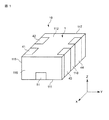
図1は、本発明の第1実施形態の電子部品を示す斜視図である。図2は、電子部品の断面図である。図3は、電子部品の分解斜視図である。図1と図2と図3に示すように、電子部品10は、積層体1と、積層体1内に設けられている回路素子2と、積層体1内に設けられている静電気放電素子3と、静電気放電素子3と回路素子2とを電気的に接続する第1〜第4回路素子用外部電極41〜44と、静電気放電素子3に接続され、静電気放電素子3をグランドに電気的に接続するための第1、第2グランド用外部電極51,52とを有する。
(First embodiment)
FIG. 1 is a perspective view showing an electronic component according to a first embodiment of the present invention. FIG. 2 is a cross-sectional view of the electronic component. FIG. 3 is an exploded perspective view of the electronic component. As shown in FIGS. 1, 2, and 3, the
電子部品10は、実装基板6に電気的に接続される。電子部品10は、例えば、パソコン、DVDプレーヤー、デジカメ、TV、携帯電話、カーエレクトロニクスなどの電子機器に搭載される。
The
積層体1は、積層された複数の絶縁層を含む。絶縁層は、非磁性体11と磁性体12とを含む。非磁性体11は、例えば、樹脂材、ガラス材、ガラスセラミックス等から構成される。磁性体12は、フェライト等の磁性体材料から構成される。好ましくは、絶縁層は、金属磁性粉を含み、これにより、電子部品10の特性(インダクタンス値や直流重畳特性等)を向上させることができる。
The
積層体1は、略直方体状に形成されている。積層体1の積層方向をZ軸方向と定義し、積層体1の長辺に沿った方向をX軸方向と定義し、積層体1の短辺に沿った方向をY軸方向と定義する。X軸とY軸とZ軸は、互いに直交している。図中上側をZ軸方向の上方向とし、図中下側をZ軸方向の下方向とする。
The
積層体1の表面は、第1端面111と第2端面112と第1側面115と第2側面116と第3側面117と第4側面118とを有する。第1端面111と第2端面112とは、積層方向(Z軸方向)に互いに反対側に位置する。第1〜第4側面115〜118は、第1端面111と第2端面112との間に、位置する。
The surface of the
第1端面111は、実装基板6に実装される被実装面であり、下側に位置する。第1側面115と第3側面117とは、それぞれ短側面であり、X軸方向に互いに反対側に位置する。第2側面116と第4側面118とは、それぞれ長側面であり、Y軸方向に互いに反対側に位置する。
The
回路素子2は、コモンドチョークコイルである。回路素子2は、上から下に向かって順に第1〜第4コイル21〜24を含む。第1〜第4コイル21〜24は、それぞれ、非磁性体シート11a上に設けられる。第1〜第4コイル21〜24は、例えば、Ag、Ag−Pd、Cu、Ni等の導電性材料から構成される。第1〜第4コイル21〜24は、例えば、導電性材料を非磁性体シート11a上に印刷し焼き付けて、形成される。
The
第1〜第4コイル21〜24は、上方からみて、同一方向に螺旋状に巻き回されている。第1コイル21の螺旋状の外周側の一端は、引出電極21aを有し、第1コイル21の螺旋状の中心の他端は、ビアホール導体21bを有する。同様に、第2コイル22は、引出電極22aとビアホール導体22bとを有し、第3コイル23は、引出電極23aとビアホール導体23bとを有し、第4コイル24は、引出電極24aとビアホール導体24bとを有する。
The first to
第1コイル21の引出電極21aは、第2側面116の第1側面115側から露出し、第2コイル22の引出電極22aは、第2側面116の第3側面117側から露出し、第3コイル23の引出電極23aは、第4側面118の第1側面115側から露出し、第4コイル24の引出電極24aは、第4側面118の第3側面117側から露出する。
The
第1コイル21のビアホール導体21bと第3コイル23のビアホール導体23bとは、電気的に接続される。第2コイル22のビアホール導体22bと第4コイル24のビアホール導体24bとは、電気的に接続される。
The via
静電気放電素子(ESD(Electro-Static Discharge)素子)3は、第1〜第5放電電極31〜35を含む。第1〜第5放電電極31〜35は、上下の非磁性体シート11aに挟まれている。第1〜第4放電電極31〜34は、Y軸方向に延在する。第5放電電極35は、X軸方向に延在する。
The electrostatic discharge element (ESD (Electro-Static Discharge) element) 3 includes first to
第1放電電極31の一端部は、第2側面116の第1側面115側から露出し、第1放電電極31の他端部は、非磁性体11のY方向の中央に位置する。第2放電電極32の一端部は、第2側面116の第3側面117側から露出し、第2放電電極32の他端部は、非磁性体11のY方向の中央に位置する。
One end portion of the
第3放電電極33の一端部は、第4側面118の第1側面115側から露出し、第3放電電極33の他端部は、非磁性体11のY方向の中央に位置する。第4放電電極34の一端部は、第4側面118の第3側面117側から露出し、第4放電電極34の他端部は、非磁性体11のY方向の中央に位置する。
One end portion of the third discharge electrode 33 is exposed from the
第5放電電極35の一端部は、第1放電電極31の他端部と第3放電電極33の他端部との間の隙間に、位置する。第5放電電極35の一端部と第1放電電極31の他端部との間には、放電用の隙間が設けられている。第5放電電極35の一端部と第3放電電極33の他端部との間には、放電用の隙間が設けられている。
One end of the
第5放電電極35の他端部は、第2放電電極32の他端部と第4放電電極34の他端部との間の隙間に、位置する。第5放電電極35の他端部と第2放電電極32の他端部との間には、放電用の隙間が設けられている。第5放電電極35の他端部と第4放電電極34の他端部との間には、放電用の隙間が設けられている。
The other end of the
なお、放電用の隙間には、如何なる部材が存在しないようにしてもよく、または、放電しやすい材料が充填されていてもよい。放電しやすい材料の一例として、コーティング粒子と半導体粒子とを含む。コーティング粒子は、Cu等の金属粒子の表面がアルミナ等の無機材料でコーティングされている粒子である。半導体粒子は、SiC等の半導体材料の粒子である。コーティング粒子と半導体粒子とは、分散して配置されているのが好ましい。コーティング粒子と半導体粒子とを分散することで、ショートの防止や、放電開始電圧等のESD特性の調整が容易となる。 Note that any member may not be present in the discharge gap, or a material that is easily discharged may be filled therein. An example of a material that is easily discharged includes coating particles and semiconductor particles. The coating particles are particles in which the surface of metal particles such as Cu is coated with an inorganic material such as alumina. The semiconductor particles are particles of a semiconductor material such as SiC. The coating particles and the semiconductor particles are preferably arranged in a dispersed manner. Dispersion of the coating particles and the semiconductor particles facilitates prevention of short circuit and adjustment of ESD characteristics such as a discharge start voltage.
第5放電電極35の一端部は、第1側面115から露出し、第5放電電極35の他端部は、第3側面117から露出する。
One end portion of the
静電気放電素子3は、回路素子2よりも、積層体1の第1端面111側(下側)に配置される。回路素子2を覆う回路側の非磁性体11と静電気放電素子3を覆う放電側の非磁性体11とは、上下の磁性体12,12で、挟まれる。回路側の非磁性体11と放電側の非磁性体11との間には、磁性体12が配置される。
The
第1〜第4回路素子用外部電極41〜44は、例えば、Ag、Ag−Pd、Cu、Ni等の導電性材料から構成される。第1〜第4回路素子用外部電極41〜44は、例えば、導電性材料を積層体1の表面に塗布し焼き付けて、形成される。第1〜第4回路素子用外部電極41〜44は、それぞれ、コ字状に形成される。
The first to fourth circuit element
第1回路素子用外部電極41は、第2側面116の第1側面115側に設けられる。第1回路素子用外部電極41の一端部は、第2側面116側から折り返されて、第1端面111に設けられる。第1回路素子用外部電極41の他端部は、第2側面116側から折り返されて、第2端面112に設けられる。第1回路素子用外部電極41は、回路素子2の第1コイル21の引出電極21aと、静電気放電素子3の第1放電電極31の一端部とを、電気的に接続する。
The
第2回路素子用外部電極42は、第2側面116の第3側面117側に設けられる。第2回路素子用外部電極42の形状は、第1回路素子用外部電極41の形状と同じであるので、その説明を省略する。第2回路素子用外部電極42は、回路素子2の第2コイル22の引出電極22aと、静電気放電素子3の第2放電電極32の一端部とを、電気的に接続する。
The second circuit element
第3回路素子用外部電極43は、第4側面118の第1側面115側に設けられる。第2回路素子用外部電極43の形状は、第1回路素子用外部電極41の形状と同じであるので、その説明を省略する。第3回路素子用外部電極43は、回路素子2の第3コイル23の引出電極23aと、静電気放電素子3の第3放電電極33の一端部とを、電気的に接続する。
The third circuit element
第4回路素子用外部電極44は、第4側面118の第3側面117側に設けられる。第4回路素子用外部電極44の形状は、第1回路素子用外部電極41の形状と同じであるので、その説明を省略する。第4回路素子用外部電極44は、回路素子2の第4コイル24の引出電極24aと、静電気放電素子3の第4放電電極34の一端部とを、電気的に接続する。
The fourth circuit element
第1、第2グランド用外部電極51,52は、例えば、Ag、Ag−Pd、Cu、Ni等の導電性材料から構成される。第1、第2グランド用外部電極51,52は、例えば、導電性材料を積層体1の表面の凹部に塗布し焼き付けて、形成される。第1、第2グランド用外部電極51,52は、それぞれ、L字状に形成される。
The first and second ground
第1グランド用外部電極51は、第1端面111から第1側面115に渡って設けられる。第1グランド用外部電極51は、第5放電電極35の一端部と、実装基板6の図示しないグランド用配線とを、電気的に接続する。
The first ground
第1グランド用外部電極51は、第5放電電極35から下側に延在する。第5放電電極35の下側に位置する非磁性体11および磁性体12は、それぞれ、第1側面115側に、凹部11b,12bを有する。非磁性体11の凹部11bと磁性体12の凹部12bとは、一体に連続している。凹部11b,12bは、第1端面115から切り欠かれると共に第1端面111から第2端面112に向かって延在する。第1グランド用外部電極51は、凹部11b,12bに嵌め込まれている。つまり、第1グランド用外部電極51の一部は、積層体1の第1側面115から露出する。
The first ground
第2グランド用外部電極52は、第1端面111から第3側面117に渡って設けられる。第2グランド用外部電極52は、第5放電電極35の他端部と、実装基板6の図示しないグランド用配線とを、電気的に接続する。
The second ground
第2グランド用外部電極52は、第5放電電極35から下側に延在する。第5放電電極35の下側に位置する非磁性体11および磁性体12は、それぞれ、第3側面117側に、凹部11b,12bを有する。凹部11b,12bは、第1端面115から切り欠かれると共に第1端面111から第2端面112に向かって延在する。第2グランド用外部電極52は、凹部11b,12bに嵌め込まれている。つまり、第2グランド用外部電極52の一部は、積層体1の第3側面117から露出する。
The second ground
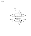
図4は、電子部品10の回路図である。図4に示すように、第1回路素子用外部電極41と第3回路素子用外部電極43との間には、第1コイル21と第3コイル23からなる第1コイル群L1が接続されている。第1コイル群L1および第1回路素子用外部電極41の間と第1グランド用外部電極51との間には、第1放電電極31および第5放電電極35からなる第1放電群E1が接続されている。第1コイル群L1および第3回路素子用外部電極43の間と第1グランド用外部電極51との間には、第3放電電極33および第5放電電極35からなる第3放電群E3が接続されている。
FIG. 4 is a circuit diagram of the
第2回路素子用外部電極42と第4回路素子用外部電極44との間には、第2コイル22と第4コイル24からなる第2コイル群L2が接続されている。第2コイル群L2および第2回路素子用外部電極42の間と第2グランド用外部電極52との間には、第2放電電極32および第5放電電極35からなる第2放電群E2が接続されている。第2コイル群L2および第4回路素子用外部電極44の間と第2グランド用外部電極52との間には、第4放電電極34および第5放電電極35からなる第4放電群E4が接続されている。
A second coil group L2 including the
図5は、電子部品10の簡略構成図である。図5に示すように、第1グランド用外部電極51の回路素子2側の端部の第1端面111からの高さH1は、回路素子2の第1グランド用外部電極51側の端部の第1端面111からの高さH2よりも、低い。具体的に述べると、第1グランド用外部電極51の上端面における第1端面111からの高さH1は、回路素子2の第4コイル24の下端面における第1端面111からの高さH2よりも、低い。なお、第2グランド用外部電極52の上端面は、第1グランド用外部電極51の上端面と同じ高さにある。
FIG. 5 is a simplified configuration diagram of the
次に、電子部品10の製造方法について説明する。
Next, a method for manufacturing the
図3に示すように、第1〜第4コイル21〜24の材料を、それぞれ異なる非磁性体シート11aに、例えば印刷等により塗布する。また、第1〜第5放電電極31〜35の材料を、別の非磁性体シート11aに、例えば印刷等により塗布する。
As shown in FIG. 3, the materials of the first to
そして、第1〜第4コイル21〜24の材料が塗布された非磁性体シート11aと、第1〜第5放電電極31〜35の材料が塗布された非磁性体シート11aと、複数の磁性体12とを、積層し熱圧着して、回路素子2および静電気放電素子3を積層体1内に設ける。
And the nonmagnetic sheet |
その後、第1〜第4回路素子用外部電極41〜44の材料を、積層体1の表面に、例えば印刷等により塗布し、第1、第2グランド用外部電極51,52の材料を、積層体1の表面に、例えば印刷等により塗布し、これらの材料を焼き付けて、積層体1の表面に第1〜第4回路素子用外部電極41〜44および第1、第2グランド用外部電極51,52を形成する。このようにして、電子部品10を製造する。
Thereafter, the materials of the first to fourth circuit element
前記電子部品10によれば、静電気放電素子3は、回路素子2よりも、積層体1の第1端面111側に配置され、グランド用外部電極51,52の回路素子2側の端部の第1端面111からの高さH1は、回路素子2のグランド用外部電極51,52側の端部の第1端面111からの高さH2よりも、低い。これにより、グランド用外部電極51,52は、積層方向(Z方向)に直交する平面(XY平面)において、回路素子2の少なくとも一部に重ならず、グランド用外部電極51,52は、積層方向(Z方向)において、回路素子2から離隔している。したがって、積層体1の第1端面111を実装基板6に実装して電子部品10を使用したとき、グランド用外部電極51,52と回路素子2との間に発生する浮遊容量が低減し、電気的特性(高周波特性)が向上する。なお、積層体1の第2端面112を実装基板6に実装して、電子部品10を使用することもできる。
According to the
これに対して、グランド用外部電極51,52の第1端面111からの高さH1が、回路素子2の第1端面111からの高さH2と同じであるか、または、高いと、グランド用外部電極51,52と回路素子2との間に発生する浮遊容量が増大し、電気的特性が劣化する。
On the other hand, if the height H1 from the
また、積層体1の第1端面111は、実装基板6に実装される被実装面である。したがって、静電気放電素子3が、回路素子2よりも、被実装面側に配置されるので、実装基板6へ静電気を放電しやすくなる。また、静電気放電素子3が、回路素子2よりも、被実装面側に配置されるので、電子部品10の重心が、被実装面側に近くなって、電子部品10を実装基板6に実装したときの電子部品10の姿勢が安定する。したがって、電子部品10の横転を防止できる。
In addition, the
また、グランド用外部電極51,52は、積層体1の第1端面111から側面115,117に渡って、設けられている。したがって、グランド用外部電極51,52を、半田を介して、実装基板6に実装する場合、半田は、グランド用外部電極51,52における積層体1の側面115,117に設けられる部分にも接続され、電子部品10と実装基板6との接続の信頼性が増大する。
The ground
また、グランド用外部電極51,52は、積層体1の側面115,117の凹部11b,12bに嵌め込まれている。したがって、電子部品10の積層体1の側面方向の厚みが、一定に設定されているとき、グランド用外部電極51,52の積層体1の側面115,117から露出する部分の厚みを小さくできるため、積層体1の側面方向の厚みを大きくできる。このように、積層体1の側面方向の厚みを大きくすることで、回路素子2を大きく設計することができ、回路素子2としての電気的特性(例えばインダクタンス値など)を向上させることができる。
The ground
(第2の実施形態)
図6は、本発明の第2実施形態の電子部品を示す簡略構成図である。第2実施形態は、前記第1実施形態とは、静電気放電素子と回路素子との間の距離、および、静電気放電素子と積層体の第1端面との間の距離が相違する。この相違する構成のみを以下に説明する。なお、第2実施形態において、第1実施形態と同一の符号は、第1実施形態と同じ構成であるため、その説明を省略する。
(Second Embodiment)
FIG. 6 is a simplified configuration diagram showing an electronic component according to the second embodiment of the present invention. The second embodiment is different from the first embodiment in the distance between the electrostatic discharge element and the circuit element and the distance between the electrostatic discharge element and the first end surface of the laminate. Only this different configuration will be described below. Note that in the second embodiment, the same reference numerals as those in the first embodiment have the same configurations as those in the first embodiment, and a description thereof will be omitted.
図6に示すように、静電気放電素子3と回路素子2との間の距離L1は、50μm以上である。具体的に述べると、静電気放電素子3の回路素子2側の端部(第5放電電極35の上端面)と、回路素子2の静電気放電素子3側の端部(第4コイル24の下端面)との間の距離L1は、50μm以上である。
As shown in FIG. 6, the distance L1 between the
したがって、静電気放電素子3と回路素子2との間の距離L1は、50μm以上であるので、静電気放電素子3が回路素子2から離隔して、静電気放電素子3と回路素子2との間の絶縁層(磁性体12)は、厚くなる。これにより、コモンモードインピーダンスが高くなり、ノイズ除去効果が向上する。
Therefore, since the distance L1 between the
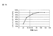
図7Aは、距離L1とコモンインピーダンスとの関係を示す。横軸に距離L1[μm]を示し、縦軸に100MHzでのコモンインピーダンス[%]を示す。図7Aに示すように、距離L1が50μm以上であると、コモンモードインピーダンスが高くなっている。これに対して、距離L1が、50μmよりも小さくなると、コモンモードインピーダンスが低くなる。 FIG. 7A shows the relationship between the distance L1 and the common impedance. The horizontal axis indicates the distance L1 [μm], and the vertical axis indicates the common impedance [%] at 100 MHz. As shown in FIG. 7A, when the distance L1 is 50 μm or more, the common mode impedance is high. On the other hand, when the distance L1 is smaller than 50 μm, the common mode impedance is lowered.
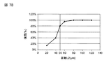
図6に示すように、静電気放電素子3と積層体1の第1端面111との間の距離L2は、50μm以上である。具体的に述べると、静電気放電素子3の第1端面111側の端部(第5放電電極35の下端面)と第1端面111との間の距離L2は、50μm以上である。
As shown in FIG. 6, the distance L2 between the
ここで、静電気放電素子3により静電気の放電を行うために、静電気放電素子3を構成する第1〜第5放電電極31〜35間に空隙を設ける必要がある。静電気放電素子3と第1端面111との間の距離L2は、50μm以上であるので、この放電電極31〜35間の空隙を、積層体1の第1端面111から離隔することができる。したがって、積層体1の第1端面111を実装基板6に実装する時に、電子部品10に衝撃等が発生しても、電子部品10にワレ、カケ、クラックが発生することを防止できる。
Here, in order to discharge static electricity with the
図7Bは、距離L2と電子部品10の強度との関係を示す。横軸に距離L2[μm]を示し、縦軸に電子部品10の強度[%]を示す。図7Bに示すように、距離L2が50μm以上であると、電子部品10の強度が大きくなっている。これに対して、距離L2が、50μmよりも小さくなると、電子部品10の強度が小さくなる。
FIG. 7B shows the relationship between the distance L2 and the strength of the
(第3の実施形態)
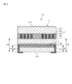
図8は、本発明の第3実施形態の電子部品を示す簡略構成図である。第3実施形態は、前記第1実施形態とは、グランド用外部電極の形状が相違する。この相違する構成のみを以下に説明する。なお、第3実施形態において、第1実施形態と同一の符号は、第1実施形態と同じ構成であるため、その説明を省略する。
(Third embodiment)
FIG. 8 is a simplified configuration diagram showing an electronic component according to a third embodiment of the present invention. The third embodiment is different from the first embodiment in the shape of the ground external electrode. Only this different configuration will be described below. Note that in the third embodiment, the same reference numerals as those in the first embodiment have the same configurations as those in the first embodiment, and a description thereof will be omitted.
図8に示すように、第3実施形態の電子部品10Bでは、積層体1Bの側面115,117には、第1端面111から切り欠かれると共に第1端面111から第2端面112に向かって延在する凹部121b,122bを有する。第1グランド用外部電極51Bは、積層体1Bの凹部121bに嵌め込まれている。第2グランド用外部電極52Bは、積層体1Bの凹部122bに嵌め込まれている。
As shown in FIG. 8, in the
第1グランド用外部電極51Bにおける積層体1Bの凹部121bの内面に接触する接触部分51bの形状は、第1端面111から第2端面112に向かって延在する階段状である。積層体1Bの凹部121bの内面における第1グランド用外部電極51Bに接触する接触部分1bの形状は、第1端面111から第2端面112に向かって延在する階段状である。第1グランド用外部電極51Bの接触部分51bと積層体1B内面の接触部分1bとは、互いに、係合する。
The shape of the
同様に、第2グランド用外部電極52Bの積層体1Bの凹部122bの内面に接触する接触部分52bの形状は、階段状である。積層体1Bの凹部122bの内面の第2グランド用外部電極52Bに接触する接触部分2bの形状は、階段状である。第2グランド用外部電極52Bの接触部分52bと積層体1B内面の接触部分2bとは、互いに、係合する。
Similarly, the shape of the
したがって、第1、第2グランド用外部電極51B,52Bの階段状の接触部分51b,52bと積層体1B内面の階段状の接触部分1b,2bとは、互いに、係合するので、第1、第2グランド用外部電極51B,52Bは、積層体1B内面から外れにくくなる。
Accordingly, the step-
次に、第1、第2グランド用外部電極51B,52Bの製造方法について説明する。
Next, a method for manufacturing the first and second ground
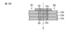
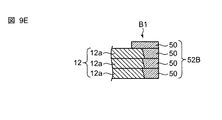
図9Aに示すように、磁性体シート12aを用意し、図9Bに示すように、レーザ等の工法により、磁性体シート12aに孔12cを設ける。このとき、孔12cの内面は、テーパ状に形成される。図9Cに示すように、孔12c内に、Ag等の導電性材料50を充填印刷する。
As shown in FIG. 9A, a
その後、図9Dに示すように、導電性材料50が印刷された磁性体シート12aを複数積層し、最上部の磁性体シート12aの上面に、導電性材料50を印刷する。このとき、複数の磁性体シート12aの孔12cの中心は、一致する。これにより、複数の磁性体シート12aの導電性材料50は、積層されて、接続される。
Thereafter, as shown in FIG. 9D, a plurality of
その後、磁性体シート12aの孔12cの中心Cでカットして2つの部材B1,B2に分割して、図9Eに示すように、一方の部材B1を選択する。図9Fに示すように、一方の部材B1を反転して、磁性体12に埋め込まれた第2グランド用外部電極52Bを製造する。このとき、磁性体シート12aに孔12cの内面は、テーパ状に形成されているため、第2グランド用外部電極52Bの接触部分52bの形状は、階段状となり、積層体1Bの凹部122bの内面の接触部分2bの形状は、階段状となる。なお、他方の部材B2も一方の部材B1と同様に製造する。また、第1グランド用外部電極51Bも第2グランド用外部電極52Bと同様に製造する。
After that, it is cut at the center C of the
(第4の実施形態)
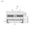
図10は、本発明の第4実施形態の電子部品を示す簡略構成図である。第4実施形態は、前記第1実施形態とは、グランド用外部電極の形状が相違する。この相違する構成のみを以下に説明する。なお、第4実施形態において、第1実施形態と同一の符号は、第1実施形態と同じ構成であるため、その説明を省略する。
(Fourth embodiment)
FIG. 10 is a simplified configuration diagram showing an electronic component according to a fourth embodiment of the present invention. The fourth embodiment differs from the first embodiment in the shape of the ground external electrode. Only this different configuration will be described below. In addition, in 4th Embodiment, since the code | symbol same as 1st Embodiment is the same structure as 1st Embodiment, the description is abbreviate | omitted.
図10に示すように、第4実施形態の電子部品10Cでは、積層体1Cの第1端面111には、第1端面111に開口を有すると共に第1端面111から第2端面112に向かって延在する孔部131c,132cを有する。第1グランド用外部電極51Cは、積層体1Cの孔部131cに嵌め込まれている。第2グランド用外部電極52Cは、積層体1Cの孔部132cに嵌め込まれている。つまり、第1、第2グランド用外部電極51C,52Cは、積層体1Cの側面115,117から露出しない。
As shown in FIG. 10, in the
したがって、電子部品10の積層体1Cの側面方向の厚みが、一定に設定されているとき、第1、第2グランド用外部電極51C,52Cの積層体1Cの側面115,117から露出する部分の厚みをなくすことができるため、積層体1Cの側面方向の厚みを大きくできる。このように、積層体1Cの側面方向の厚みを大きくすることで、回路素子2を大きく設計することができ、回路素子2としての電気的特性を向上させることができる。また、第1、第2グランド用外部電極51C,52Cは、積層体1C内に覆われているので、他の電子部品や装置等との接触による第1、第2グランド用外部電極51C,52Cの損傷を防止できる。
Therefore, when the thickness in the side surface direction of the
第1グランド用外部電極51Cにおける積層体1Cの孔部131cの内面に接触する接触部分51cの形状は、第1端面111から第2端面112に向かって延在する階段状である。積層体1Cの孔部131cの内面における第1グランド用外部電極51Cに接触する接触部分1cの形状は、第1端面111から第2端面112に向かって延在する階段状である。第1グランド用外部電極51Cの接触部分51cと積層体1C内面の接触部分1cとは、互いに、係合する。
The shape of the
同様に、第2グランド用外部電極52Cの積層体1Cの孔部132cの内面に接触する接触部分52cの形状は、階段状である。積層体1Cの孔部132cの内面の第2グランド用外部電極52Cに接触する接触部分2cの形状は、階段状である。第2グランド用外部電極52Cの接触部分52cと積層体1C内面の接触部分2cとは、互いに、係合する。
Similarly, the shape of the
したがって、第1、第2グランド用外部電極51C,52Cの階段状の接触部分51c,52cと積層体1C内面の階段状の接触部分1c,2cとは、互いに、係合するので、第1、第2グランド用外部電極51C,52Cは、積層体1C内面から外れにくくなる。
Accordingly, the step-
次に、第1、第2グランド用外部電極51C,52Cの製造方法について説明する。
Next, a method for manufacturing the first and second ground
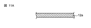
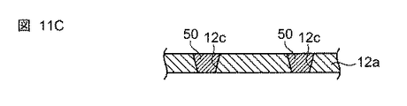
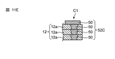
図11Aに示すように、磁性体シート12aを用意し、図11Bに示すように、レーザ等の工法により、磁性体シート12aに隣り合う2つの孔12cを設ける。このとき、孔12cの内面は、テーパ状に形成される。図11Cに示すように、孔12c内に、Ag等の導電性材料50を充填印刷する。
As shown in FIG. 11A, a
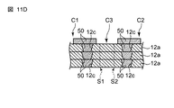
その後、図11Dに示すように、導電性材料50が印刷された磁性体シート12aを複数積層し、最上部の磁性体シート12aの上面に、導電性材料50を印刷する。このとき、複数の磁性体シート12aの孔12cの中心は、一致する。これにより、複数の磁性体シート12aの導電性材料50は、積層されて、接続される。
Thereafter, as shown in FIG. 11D, a plurality of
その後、隣り合う2つの孔12cの間に位置する2箇所の切断部S1,S2でカットして3つの部材C1,C2,C3に分割する。第1部材C1と第2部材C2とは、それぞれ、導電性材料50を含む部材である。第3部材C3は、第1部材C1と第2部材C2との間に位置し、導電性材料50を含まないカット代となる。
Then, it cut | disconnects by two cut part S1, S2 located between the two
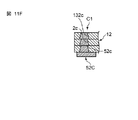
その後、図11Eに示すように、第1部材C1を選択する。図11Fに示すように、第1部材C1を反転して、磁性体12に埋め込まれた第2グランド用外部電極52Cを製造する。このとき、磁性体シート12aに孔12cの内面は、テーパ状に形成されているため、第2グランド用外部電極52Cの接触部分52cの形状は、階段状となり、積層体1Cの孔部132cの内面の接触部分2cの形状は、階段状となる。なお、第2部材C2も第1部材C1と同様に製造する。また、第1グランド用外部電極51Cも第2グランド用外部電極52Cと同様に製造する。
Thereafter, as shown in FIG. 11E, the first member C1 is selected. As shown in FIG. 11F, the first member C1 is inverted, and the second ground
なお、本発明は上述の実施形態に限定されず、本発明の要旨を逸脱しない範囲で設計変更可能である。例えば、前記第1から前記第4実施形態のそれぞれの特徴点を様々に組み合わせてもよい。 The present invention is not limited to the above-described embodiment, and the design can be changed without departing from the gist of the present invention. For example, the feature points of the first to fourth embodiments may be variously combined.
前記実施形態では、回路素子としては、4つのコイルを用いたが、2つのコイルを用いてもよい。前記実施形態では、回路素子としては、コモンドチョークコイルとしたが、他のコイルとしてもよい。 In the embodiment, four coils are used as circuit elements, but two coils may be used. In the embodiment, the circuit element is a common choke coil, but may be another coil.
前記実施形態では、静電気放電素子と回路素子との間の距離が50μm以上であるか、または、静電気放電素子と積層体の第1端面との間の距離が50μm以上であるか、何れか一方であってもよい。 In the embodiment, either the distance between the electrostatic discharge element and the circuit element is 50 μm or more, or the distance between the electrostatic discharge element and the first end face of the laminate is 50 μm or more. It may be.
前記実施形態では、静電気放電素子を回路素子よりも実装基板側に配置したが、電子部品を上下反転させ、回路素子を静電気放電素子よりも実装基板側に配置するようにしてもよい。このとき、静電気放電素子は使用されない。 In the above-described embodiment, the electrostatic discharge element is disposed on the mounting substrate side with respect to the circuit element. However, the electronic component may be turned upside down so that the circuit element is disposed on the mounting substrate side with respect to the electrostatic discharge element. At this time, the electrostatic discharge element is not used.
1,1B,1C 積層体
1b,1c,2b,2c 接触部分
2 回路素子
3 静電気放電素子
6 実装基板
10,10A,10B,10C 電子部品
11 非磁性体(絶縁層)
12 磁性体(絶縁層)
111 第1端面
112 第2端面
115〜118 第1〜第4側面
21〜24 第1〜第4コイル
31〜35 第1〜第5放電電極
41〜44 第1〜第4回路素子用外部電極
51,51B,51C 第1グランド用外部電極
52,52B,52C 第2グランド用外部電極
51b,51c,52b,52c 接触部分
11b,12b,121b,122b 凹部
131c,132c 孔部
H1 グランド用外部電極の積層体の第1端面からの高さ
H2 回路素子の積層体の第1端面からの高さ
L1 静電気放電素子と回路素子との間の距離
L2 静電気放電素子と積層体の第1端面との間の距離
1, 1B,
12 Magnetic material (insulating layer)
111
Claims (11)
前記積層体内に設けられている回路素子と、
前記積層体内に設けられている静電気放電素子と、
前記静電気放電素子と前記回路素子とを電気的に接続する回路素子用外部電極と、
前記静電気放電素子に接続され、前記静電気放電素子をグランドに電気的に接続するためのグランド用外部電極と
を備え、
前記積層体は、前記絶縁層の積層方向に位置すると共に互いに反対側に位置する第1端面と第2端面とを有し、
前記静電気放電素子は、前記回路素子よりも、前記積層体の前記第1端面側に配置され、
前記回路素子用外部電極は、前記積層体の前記第1端面と前記第2端面との間の側面と、前記側面から折り返されて前記第1端面と、前記側面から折り返されて前記第2端面とに設けられ、
前記グランド用外部電極は、前記積層体の前記第1端面から、前記積層体の前記第1端面と前記第2端面との間の側面に渡って、設けられ、
前記グランド用外部電極の前記回路素子側の端部の前記第1端面からの高さは、前記回路素子の前記グランド用外部電極側の端部の前記第1端面からの高さよりも、低いことを特徴とする電子部品。 A laminate including a plurality of laminated insulating layers;
A circuit element provided in the laminate;
An electrostatic discharge element provided in the laminate;
An external electrode for a circuit element that electrically connects the electrostatic discharge element and the circuit element;
An external electrode for ground connected to the electrostatic discharge element, for electrically connecting the electrostatic discharge element to the ground,
The stacked body has a first end surface and a second end surface that are positioned in the stacking direction of the insulating layer and located on opposite sides of each other,
The electrostatic discharge element is disposed on the first end face side of the multilayer body than the circuit element,
The external electrode for a circuit element includes a side surface between the first end surface and the second end surface of the laminate, a first end surface folded from the side surface, and a second end surface folded from the side surface. And
The ground external electrode is provided from the first end surface of the multilayer body to a side surface between the first end surface and the second end surface of the multilayer body,
The height of the end on the circuit element side of the ground external electrode from the first end face is lower than the height of the end on the ground external electrode side of the circuit element from the first end face. Electronic parts characterized by
前記絶縁層は、非磁性体と磁性体とを含み、前記回路素子と前記静電気放電素子は、それぞれ、前記非磁性体に覆われ、前記回路素子を覆う前記非磁性体と前記静電気放電素子を覆う前記非磁性体との間には、前記磁性体が配置されることを特徴とする電子部品。 The insulating layer includes a non-magnetic body and a magnetic body, and the circuit element and the electrostatic discharge element are covered with the non-magnetic body, and the non-magnetic body and the electrostatic discharge element covering the circuit element, respectively. An electronic component, wherein the magnetic body is disposed between the non-magnetic body to be covered.
前記積層体の前記第1端面は、実装基板に実装される被実装面であることを特徴とする電子部品。 The electronic component according to claim 1 or 2 ,
The electronic component according to claim 1, wherein the first end surface of the laminate is a mounted surface to be mounted on a mounting substrate.
前記積層体の前記側面には、前記第1端面から切り欠かれると共に前記第1端面から前記第2端面に向かって延在する凹部を有し、
前記グランド用外部電極は、前記積層体の前記凹部に嵌め込まれていることを特徴とする電子部品。 The electronic component according to claim 3,
The side surface of the laminate has a recess that is notched from the first end surface and extends from the first end surface toward the second end surface,
The ground external electrode is fitted in the concave portion of the multilayer body.
前記グランド用外部電極における前記積層体の前記凹部の内面に接触する接触部分の形状は、前記第1端面から前記第2端面に向かって延在する階段状であり、
前記積層体の前記凹部の内面における前記グランド用外部電極に接触する接触部分の形状は、前記第1端面から前記第2端面に向かって延在する階段状であり、
前記グランド用外部電極の前記接触部分と前記積層体の前記接触部分とは、互いに、係合することを特徴とする電子部品。 The electronic component according to claim 4,
The shape of the contact portion that contacts the inner surface of the concave portion of the laminate in the ground external electrode is a stepped shape extending from the first end surface toward the second end surface,
The shape of the contact portion in contact with the ground external electrode on the inner surface of the concave portion of the laminate is a stepped shape extending from the first end surface toward the second end surface,
The electronic component according to claim 1, wherein the contact portion of the ground external electrode and the contact portion of the laminate are engaged with each other.
前記積層体の前記第1端面には、前記第1端面に開口を有すると共に前記第1端面から前記第2端面に向かって延在する孔部を有し、
前記グランド用外部電極は、前記積層体の前記孔部に嵌め込まれていることを特徴とする電子部品。 The electronic component according to claim 1 or 2,
The first end surface of the laminate has an opening in the first end surface and a hole extending from the first end surface toward the second end surface,
The ground external electrode is fitted in the hole of the multilayer body.
前記グランド用外部電極における前記積層体の前記孔部の内面に接触する接触部分の形状は、前記第1端面から前記第2端面に向かって延在する階段状であり、
前記積層体の前記孔部の内面における前記グランド用外部電極に接触する接触部分の形状は、前記第1端面から前記第2端面に向かって延在する階段状であり、
前記グランド用外部電極の前記接触部分と前記積層体の前記接触部分とは、互いに、係合することを特徴とする電子部品。 The electronic component according to claim 6,
The shape of the contact portion in contact with the inner surface of the hole of the laminate in the ground external electrode is a stepped shape extending from the first end surface toward the second end surface,
The shape of the contact portion in contact with the ground external electrode on the inner surface of the hole of the laminate is a stepped shape extending from the first end surface toward the second end surface,
The electronic component according to claim 1, wherein the contact portion of the ground external electrode and the contact portion of the laminate are engaged with each other.
前記静電気放電素子と前記回路素子との間の距離は、50μm以上であることを特徴とする電子部品。 The electronic component according to any one of claims 1 to 7,
The distance between the said electrostatic discharge element and the said circuit element is 50 micrometers or more, The electronic component characterized by the above-mentioned.
前記静電気放電素子と前記積層体の前記第1端面との間の距離は、50μm以上であることを特徴とする電子部品。 The electronic component according to any one of claims 1 to 8,
The distance between the said electrostatic discharge element and the said 1st end surface of the said laminated body is 50 micrometers or more, The electronic component characterized by the above-mentioned.
前記絶縁層は、金属磁性粉を含むことを特徴とする電子部品。 The electronic component according to any one of claims 1 to 9,
The said insulating layer contains a metal magnetic powder, The electronic component characterized by the above-mentioned.
前記静電気放電素子と前記回路素子との間の距離は、50μm以上で120μm以下であることを特徴とする電子部品。 The distance between the said electrostatic discharge element and the said circuit element is 50 micrometers or more and 120 micrometers or less, The electronic component characterized by the above-mentioned.
Priority Applications (4)
| Application Number | Priority Date | Filing Date | Title |
|---|---|---|---|
| JP2014205136A JP6252425B2 (en) | 2014-10-03 | 2014-10-03 | Electronic components |
| KR1020150132535A KR101667888B1 (en) | 2014-10-03 | 2015-09-18 | Electronic component |
| CN201510633047.6A CN105489341A (en) | 2014-10-03 | 2015-09-29 | Electronic component |
| US14/872,823 US20160099102A1 (en) | 2014-10-03 | 2015-10-01 | Electronic component |
Applications Claiming Priority (1)
| Application Number | Priority Date | Filing Date | Title |
|---|---|---|---|
| JP2014205136A JP6252425B2 (en) | 2014-10-03 | 2014-10-03 | Electronic components |
Publications (2)
| Publication Number | Publication Date |
|---|---|
| JP2016076556A JP2016076556A (en) | 2016-05-12 |
| JP6252425B2 true JP6252425B2 (en) | 2017-12-27 |
Family
ID=55633270
Family Applications (1)
| Application Number | Title | Priority Date | Filing Date |
|---|---|---|---|
| JP2014205136A Active JP6252425B2 (en) | 2014-10-03 | 2014-10-03 | Electronic components |
Country Status (4)
| Country | Link |
|---|---|
| US (1) | US20160099102A1 (en) |
| JP (1) | JP6252425B2 (en) |
| KR (1) | KR101667888B1 (en) |
| CN (1) | CN105489341A (en) |
Families Citing this family (13)
| Publication number | Priority date | Publication date | Assignee | Title |
|---|---|---|---|---|
| KR101630083B1 (en) * | 2014-12-03 | 2016-06-13 | 삼성전기주식회사 | Coil component |
| KR20170109782A (en) * | 2016-03-22 | 2017-10-10 | 삼성전기주식회사 | Complex electronic component |
| US10529661B2 (en) * | 2016-05-05 | 2020-01-07 | Cyntec Co., Ltd | Multilayer inductor and the fabrication method thereof |
| JP6696483B2 (en) * | 2017-07-10 | 2020-05-20 | 株式会社村田製作所 | Coil parts |
| US11424070B2 (en) * | 2018-06-19 | 2022-08-23 | Tdk Corporation | Coil component |
| JP2020061410A (en) * | 2018-10-05 | 2020-04-16 | 株式会社村田製作所 | Multilayer electronic component |
| JP6919641B2 (en) | 2018-10-05 | 2021-08-18 | 株式会社村田製作所 | Laminated electronic components |
| JP6981389B2 (en) | 2018-10-05 | 2021-12-15 | 株式会社村田製作所 | Stacked coil array for DC-DC converter and DC-DC converter |
| JP6977694B2 (en) * | 2018-10-05 | 2021-12-08 | 株式会社村田製作所 | Laminated coil array |
| KR102662845B1 (en) * | 2018-11-22 | 2024-05-03 | 삼성전기주식회사 | Inductor |
| JP6908214B1 (en) * | 2019-12-25 | 2021-07-21 | 株式会社村田製作所 | Multi-terminal chip inductor |
| JP7590904B2 (en) * | 2021-03-31 | 2024-11-27 | Tdk株式会社 | Multilayer Electronic Components |
| JP2023034657A (en) * | 2021-08-31 | 2023-03-13 | Tdk株式会社 | Electronic component |
Family Cites Families (26)
| Publication number | Priority date | Publication date | Assignee | Title |
|---|---|---|---|---|
| US5610565A (en) * | 1994-02-02 | 1997-03-11 | Murata Manufacturing Co., Ltd. | Composite LC device with a ground electrode not formed on the inductor parts |
| WO2002073641A1 (en) * | 2001-03-08 | 2002-09-19 | Matsushita Electric Industrial Co., Ltd. | Inductor part, and method of producing the same |
| JP2002270429A (en) * | 2001-03-14 | 2002-09-20 | Matsushita Electric Ind Co Ltd | Inductor components |
| US7260890B2 (en) * | 2002-06-26 | 2007-08-28 | Georgia Tech Research Corporation | Methods for fabricating three-dimensional all organic interconnect structures |
| JP3900104B2 (en) * | 2003-04-10 | 2007-04-04 | 松下電器産業株式会社 | Antistatic parts |
| KR100668977B1 (en) * | 2005-06-27 | 2007-01-16 | 삼성전자주식회사 | Surge voltage protection device |
| WO2007029615A1 (en) * | 2005-09-07 | 2007-03-15 | Matsushita Electric Industrial Co., Ltd. | Composite electronic device |
| JP4725343B2 (en) | 2006-02-07 | 2011-07-13 | パナソニック株式会社 | Composite electronic component and manufacturing method thereof |
| US8493704B2 (en) * | 2007-04-11 | 2013-07-23 | Innochips Technology Co., Ltd. | Circuit protection device and method of manufacturing the same |
| KR100845948B1 (en) * | 2007-04-11 | 2008-07-11 | 주식회사 이노칩테크놀로지 | Circuit protection device and manufacturing method thereof |
| JP2010028695A (en) | 2008-07-24 | 2010-02-04 | Murata Mfg Co Ltd | Noise filter component and coil component |
| US8422190B2 (en) * | 2008-09-30 | 2013-04-16 | Tdk Corporation | Composite electronic device, manufacturing method thereof, and connection structure of composite electronic device |
| JP2011071457A (en) * | 2008-12-22 | 2011-04-07 | Tdk Corp | Electronic component and manufacturing method of electronic component |
| JP4749482B2 (en) * | 2009-07-08 | 2011-08-17 | Tdk株式会社 | Composite electronic components |
| JP5206775B2 (en) * | 2010-11-26 | 2013-06-12 | Tdk株式会社 | Electronic components |
| JP5459291B2 (en) * | 2011-10-28 | 2014-04-02 | Tdk株式会社 | Composite electronic components |
| JP6007399B2 (en) * | 2012-02-15 | 2016-10-12 | パナソニックIpマネジメント株式会社 | Common mode noise filter |
| JP5648768B2 (en) | 2012-03-16 | 2015-01-07 | 株式会社村田製作所 | Common mode choke coil |
| CN104737245B (en) * | 2012-10-19 | 2016-12-07 | 株式会社村田制作所 | Multilayer coil component and manufacture method thereof |
| KR101719841B1 (en) * | 2012-12-10 | 2017-03-24 | 삼성전기주식회사 | Common mode filter |
| KR101445741B1 (en) | 2013-05-24 | 2014-10-07 | 주식회사 이노칩테크놀로지 | Circuit protection device |
| US9293913B2 (en) * | 2013-08-01 | 2016-03-22 | Tdk Corporation | ESD protection component and method for manufacturing ESD protection component |
| KR102004770B1 (en) * | 2013-10-31 | 2019-07-29 | 삼성전기주식회사 | Composite electronic component and board for mounting the same |
| KR20150055444A (en) * | 2013-11-13 | 2015-05-21 | 삼성전기주식회사 | Common mode filter |
| KR20150090445A (en) * | 2014-01-29 | 2015-08-06 | 주식회사 이노칩테크놀로지 | Laminated chip device |
| KR101554333B1 (en) * | 2014-03-28 | 2015-09-21 | 주식회사 이노칩테크놀로지 | Circuit protection device |
-
2014
- 2014-10-03 JP JP2014205136A patent/JP6252425B2/en active Active
-
2015
- 2015-09-18 KR KR1020150132535A patent/KR101667888B1/en active Active
- 2015-09-29 CN CN201510633047.6A patent/CN105489341A/en active Pending
- 2015-10-01 US US14/872,823 patent/US20160099102A1/en not_active Abandoned
Also Published As
| Publication number | Publication date |
|---|---|
| KR101667888B1 (en) | 2016-10-19 |
| CN105489341A (en) | 2016-04-13 |
| JP2016076556A (en) | 2016-05-12 |
| KR20160040423A (en) | 2016-04-14 |
| US20160099102A1 (en) | 2016-04-07 |
Similar Documents
| Publication | Publication Date | Title |
|---|---|---|
| JP6252425B2 (en) | Electronic components | |
| JP6332200B2 (en) | Electronic components | |
| CN106877835B (en) | Electronic component | |
| CN108109807B (en) | Electronic component | |
| KR102003604B1 (en) | Coil component | |
| US8810351B2 (en) | Chip-type coil component | |
| JP2012235080A5 (en) | ||
| US8526162B2 (en) | Feedthrough multilayer capacitor | |
| US20130020905A1 (en) | Multilayer ceramic electronic component | |
| KR20150089279A (en) | Chip-type coil component | |
| US8395881B2 (en) | Multilayer feedthrough capacitor and mounted structure of multilayer feedthrough capacitor | |
| JP6673298B2 (en) | Coil parts | |
| CN101533713B (en) | Feedthrough capacitor and mounted structure thereof | |
| KR20150089211A (en) | Chip-type Coil Component | |
| US12525381B2 (en) | Multilayer coil component | |
| JP2019054018A (en) | Coil parts | |
| JP2009170737A (en) | Electronic component | |
| WO2012153655A1 (en) | Esd protection device | |
| JP5929524B2 (en) | Multilayer capacitor | |
| CN110176343A (en) | Coil electronic building brick | |
| KR20150060522A (en) | Common mode filter and electronic device including common mode filter |
Legal Events
| Date | Code | Title | Description |
|---|---|---|---|
| RD04 | Notification of resignation of power of attorney |
Free format text: JAPANESE INTERMEDIATE CODE: A7424 Effective date: 20160215 |
|
| A621 | Written request for application examination |
Free format text: JAPANESE INTERMEDIATE CODE: A621 Effective date: 20160404 |
|
| A977 | Report on retrieval |
Free format text: JAPANESE INTERMEDIATE CODE: A971007 Effective date: 20170215 |
|
| A131 | Notification of reasons for refusal |
Free format text: JAPANESE INTERMEDIATE CODE: A131 Effective date: 20170228 |
|
| A521 | Request for written amendment filed |
Free format text: JAPANESE INTERMEDIATE CODE: A523 Effective date: 20170425 |
|
| TRDD | Decision of grant or rejection written | ||
| A01 | Written decision to grant a patent or to grant a registration (utility model) |
Free format text: JAPANESE INTERMEDIATE CODE: A01 Effective date: 20171031 |
|
| A61 | First payment of annual fees (during grant procedure) |
Free format text: JAPANESE INTERMEDIATE CODE: A61 Effective date: 20171113 |
|
| R150 | Certificate of patent or registration of utility model |
Ref document number: 6252425 Country of ref document: JP Free format text: JAPANESE INTERMEDIATE CODE: R150 |