JP6977694B2 - Laminated coil array - Google Patents
Laminated coil array Download PDFInfo
- Publication number
- JP6977694B2 JP6977694B2 JP2018190195A JP2018190195A JP6977694B2 JP 6977694 B2 JP6977694 B2 JP 6977694B2 JP 2018190195 A JP2018190195 A JP 2018190195A JP 2018190195 A JP2018190195 A JP 2018190195A JP 6977694 B2 JP6977694 B2 JP 6977694B2
- Authority
- JP
- Japan
- Prior art keywords
- coil
- magnetic
- layer
- laminated
- coil conductor
- Prior art date
- Legal status (The legal status is an assumption and is not a legal conclusion. Google has not performed a legal analysis and makes no representation as to the accuracy of the status listed.)
- Active
Links
- 239000004020 conductor Substances 0.000 claims description 184
- 239000006249 magnetic particle Substances 0.000 claims description 29
- 229910000859 α-Fe Inorganic materials 0.000 claims description 16
- 239000000203 mixture Substances 0.000 claims description 6
- 229910007565 Zn—Cu Inorganic materials 0.000 claims description 4
- TVZPLCNGKSPOJA-UHFFFAOYSA-N copper zinc Chemical compound [Cu].[Zn] TVZPLCNGKSPOJA-UHFFFAOYSA-N 0.000 claims description 4
- 238000004804 winding Methods 0.000 claims description 3
- 238000000034 method Methods 0.000 description 53
- 238000004519 manufacturing process Methods 0.000 description 33
- 239000002184 metal Substances 0.000 description 27
- 229910052751 metal Inorganic materials 0.000 description 27
- 239000000696 magnetic material Substances 0.000 description 23
- 238000010586 diagram Methods 0.000 description 20
- 239000000463 material Substances 0.000 description 13
- 239000002245 particle Substances 0.000 description 11
- 229910045601 alloy Inorganic materials 0.000 description 10
- 239000000956 alloy Substances 0.000 description 10
- 239000011347 resin Substances 0.000 description 9
- 229920005989 resin Polymers 0.000 description 9
- 239000002904 solvent Substances 0.000 description 9
- 239000000843 powder Substances 0.000 description 7
- 230000008878 coupling Effects 0.000 description 6
- 238000010168 coupling process Methods 0.000 description 6
- 238000005859 coupling reaction Methods 0.000 description 6
- 239000004014 plasticizer Substances 0.000 description 5
- 238000005498 polishing Methods 0.000 description 5
- 229910000640 Fe alloy Inorganic materials 0.000 description 4
- 239000011230 binding agent Substances 0.000 description 4
- 238000001035 drying Methods 0.000 description 4
- RRAFCDWBNXTKKO-UHFFFAOYSA-N eugenol Chemical compound COC1=CC(CC=C)=CC=C1O RRAFCDWBNXTKKO-UHFFFAOYSA-N 0.000 description 4
- 238000009413 insulation Methods 0.000 description 4
- 230000004048 modification Effects 0.000 description 4
- 238000012986 modification Methods 0.000 description 4
- 238000002360 preparation method Methods 0.000 description 4
- 238000007639 printing Methods 0.000 description 4
- 239000002270 dispersing agent Substances 0.000 description 3
- -1 etc.) Substances 0.000 description 3
- 238000010304 firing Methods 0.000 description 3
- 230000004907 flux Effects 0.000 description 3
- 238000004898 kneading Methods 0.000 description 3
- 238000010030 laminating Methods 0.000 description 3
- 238000007747 plating Methods 0.000 description 3
- 229910015902 Bi 2 O 3 Inorganic materials 0.000 description 2
- 229910001339 C alloy Inorganic materials 0.000 description 2
- 229910020599 Co 3 O 4 Inorganic materials 0.000 description 2
- XEKOWRVHYACXOJ-UHFFFAOYSA-N Ethyl acetate Natural products CCOC(C)=O XEKOWRVHYACXOJ-UHFFFAOYSA-N 0.000 description 2
- 239000001856 Ethyl cellulose Substances 0.000 description 2
- ZZSNKZQZMQGXPY-UHFFFAOYSA-N Ethyl cellulose Chemical compound CCOCC1OC(OC)C(OCC)C(OCC)C1OC1C(O)C(O)C(OC)C(CO)O1 ZZSNKZQZMQGXPY-UHFFFAOYSA-N 0.000 description 2
- 229910017082 Fe-Si Inorganic materials 0.000 description 2
- 229910017133 Fe—Si Inorganic materials 0.000 description 2
- 229910004298 SiO 2 Inorganic materials 0.000 description 2
- 229910002796 Si–Al Inorganic materials 0.000 description 2
- 229910008458 Si—Cr Inorganic materials 0.000 description 2
- 229910006404 SnO 2 Inorganic materials 0.000 description 2
- 239000000654 additive Substances 0.000 description 2
- 238000003491 array Methods 0.000 description 2
- 239000011248 coating agent Substances 0.000 description 2
- 238000000576 coating method Methods 0.000 description 2
- 229920001249 ethyl cellulose Polymers 0.000 description 2
- 235000019325 ethyl cellulose Nutrition 0.000 description 2
- 239000006112 glass ceramic composition Substances 0.000 description 2
- 230000006872 improvement Effects 0.000 description 2
- 239000012535 impurity Substances 0.000 description 2
- 230000001590 oxidative effect Effects 0.000 description 2
- 229920000139 polyethylene terephthalate Polymers 0.000 description 2
- 239000005020 polyethylene terephthalate Substances 0.000 description 2
- 238000000992 sputter etching Methods 0.000 description 2
- DHKHKXVYLBGOIT-UHFFFAOYSA-N 1,1-Diethoxyethane Chemical compound CCOC(C)OCC DHKHKXVYLBGOIT-UHFFFAOYSA-N 0.000 description 1
- VXQBJTKSVGFQOL-UHFFFAOYSA-N 2-(2-butoxyethoxy)ethyl acetate Chemical compound CCCCOCCOCCOC(C)=O VXQBJTKSVGFQOL-UHFFFAOYSA-N 0.000 description 1
- 229920002799 BoPET Polymers 0.000 description 1
- NPBVQXIMTZKSBA-UHFFFAOYSA-N Chavibetol Natural products COC1=CC=C(CC=C)C=C1O NPBVQXIMTZKSBA-UHFFFAOYSA-N 0.000 description 1
- 239000005770 Eugenol Substances 0.000 description 1
- UVMRYBDEERADNV-UHFFFAOYSA-N Pseudoeugenol Natural products COC1=CC(C(C)=C)=CC=C1O UVMRYBDEERADNV-UHFFFAOYSA-N 0.000 description 1
- 239000011354 acetal resin Substances 0.000 description 1
- 229920000180 alkyd Polymers 0.000 description 1
- WUOACPNHFRMFPN-UHFFFAOYSA-N alpha-terpineol Chemical compound CC1=CCC(C(C)(C)O)CC1 WUOACPNHFRMFPN-UHFFFAOYSA-N 0.000 description 1
- 238000004458 analytical method Methods 0.000 description 1
- 230000000669 biting effect Effects 0.000 description 1
- 238000005520 cutting process Methods 0.000 description 1
- SQIFACVGCPWBQZ-UHFFFAOYSA-N delta-terpineol Natural products CC(C)(O)C1CCC(=C)CC1 SQIFACVGCPWBQZ-UHFFFAOYSA-N 0.000 description 1
- 238000007772 electroless plating Methods 0.000 description 1
- 239000003822 epoxy resin Substances 0.000 description 1
- 229960002217 eugenol Drugs 0.000 description 1
- 238000011049 filling Methods 0.000 description 1
- 238000000227 grinding Methods 0.000 description 1
- 238000010438 heat treatment Methods 0.000 description 1
- 150000002576 ketones Chemical class 0.000 description 1
- 239000002923 metal particle Substances 0.000 description 1
- 230000003071 parasitic effect Effects 0.000 description 1
- 229920000647 polyepoxide Polymers 0.000 description 1
- 229920006324 polyoxymethylene Polymers 0.000 description 1
- 239000002994 raw material Substances 0.000 description 1
- 238000001878 scanning electron micrograph Methods 0.000 description 1
- 238000004904 shortening Methods 0.000 description 1
- 229910000679 solder Inorganic materials 0.000 description 1
- 238000003980 solgel method Methods 0.000 description 1
- 229940116411 terpineol Drugs 0.000 description 1
- 229920002554 vinyl polymer Polymers 0.000 description 1
Images


Classifications
-
- H—ELECTRICITY
- H01—ELECTRIC ELEMENTS
- H01F—MAGNETS; INDUCTANCES; TRANSFORMERS; SELECTION OF MATERIALS FOR THEIR MAGNETIC PROPERTIES
- H01F27/00—Details of transformers or inductances, in general
- H01F27/28—Coils; Windings; Conductive connections
- H01F27/32—Insulating of coils, windings, or parts thereof
- H01F27/323—Insulation between winding turns, between winding layers
-
- H—ELECTRICITY
- H01—ELECTRIC ELEMENTS
- H01F—MAGNETS; INDUCTANCES; TRANSFORMERS; SELECTION OF MATERIALS FOR THEIR MAGNETIC PROPERTIES
- H01F17/00—Fixed inductances of the signal type
- H01F17/0006—Printed inductances
- H01F17/0013—Printed inductances with stacked layers
-
- H—ELECTRICITY
- H01—ELECTRIC ELEMENTS
- H01F—MAGNETS; INDUCTANCES; TRANSFORMERS; SELECTION OF MATERIALS FOR THEIR MAGNETIC PROPERTIES
- H01F41/00—Apparatus or processes specially adapted for manufacturing or assembling magnets, inductances or transformers; Apparatus or processes specially adapted for manufacturing materials characterised by their magnetic properties
- H01F41/02—Apparatus or processes specially adapted for manufacturing or assembling magnets, inductances or transformers; Apparatus or processes specially adapted for manufacturing materials characterised by their magnetic properties for manufacturing cores, coils, or magnets
- H01F41/04—Apparatus or processes specially adapted for manufacturing or assembling magnets, inductances or transformers; Apparatus or processes specially adapted for manufacturing materials characterised by their magnetic properties for manufacturing cores, coils, or magnets for manufacturing coils
- H01F41/041—Printed circuit coils
- H01F41/046—Printed circuit coils structurally combined with ferromagnetic material
-
- C—CHEMISTRY; METALLURGY
- C04—CEMENTS; CONCRETE; ARTIFICIAL STONE; CERAMICS; REFRACTORIES
- C04B—LIME, MAGNESIA; SLAG; CEMENTS; COMPOSITIONS THEREOF, e.g. MORTARS, CONCRETE OR LIKE BUILDING MATERIALS; ARTIFICIAL STONE; CERAMICS; REFRACTORIES; TREATMENT OF NATURAL STONE
- C04B35/00—Shaped ceramic products characterised by their composition; Ceramics compositions; Processing powders of inorganic compounds preparatory to the manufacturing of ceramic products
- C04B35/01—Shaped ceramic products characterised by their composition; Ceramics compositions; Processing powders of inorganic compounds preparatory to the manufacturing of ceramic products based on oxide ceramics
- C04B35/26—Shaped ceramic products characterised by their composition; Ceramics compositions; Processing powders of inorganic compounds preparatory to the manufacturing of ceramic products based on oxide ceramics based on ferrites
- C04B35/265—Compositions containing one or more ferrites of the group comprising manganese or zinc and one or more ferrites of the group comprising nickel, copper or cobalt
-
- H—ELECTRICITY
- H01—ELECTRIC ELEMENTS
- H01F—MAGNETS; INDUCTANCES; TRANSFORMERS; SELECTION OF MATERIALS FOR THEIR MAGNETIC PROPERTIES
- H01F17/00—Fixed inductances of the signal type
- H01F17/04—Fixed inductances of the signal type with magnetic core
-
- H—ELECTRICITY
- H01—ELECTRIC ELEMENTS
- H01F—MAGNETS; INDUCTANCES; TRANSFORMERS; SELECTION OF MATERIALS FOR THEIR MAGNETIC PROPERTIES
- H01F27/00—Details of transformers or inductances, in general
- H01F27/24—Magnetic cores
- H01F27/255—Magnetic cores made from particles
-
- H—ELECTRICITY
- H01—ELECTRIC ELEMENTS
- H01F—MAGNETS; INDUCTANCES; TRANSFORMERS; SELECTION OF MATERIALS FOR THEIR MAGNETIC PROPERTIES
- H01F27/00—Details of transformers or inductances, in general
- H01F27/28—Coils; Windings; Conductive connections
- H01F27/2804—Printed windings
-
- H—ELECTRICITY
- H01—ELECTRIC ELEMENTS
- H01F—MAGNETS; INDUCTANCES; TRANSFORMERS; SELECTION OF MATERIALS FOR THEIR MAGNETIC PROPERTIES
- H01F27/00—Details of transformers or inductances, in general
- H01F27/28—Coils; Windings; Conductive connections
- H01F27/2847—Sheets; Strips
-
- H—ELECTRICITY
- H01—ELECTRIC ELEMENTS
- H01F—MAGNETS; INDUCTANCES; TRANSFORMERS; SELECTION OF MATERIALS FOR THEIR MAGNETIC PROPERTIES
- H01F27/00—Details of transformers or inductances, in general
- H01F27/28—Coils; Windings; Conductive connections
- H01F27/29—Terminals; Tapping arrangements for signal inductances
- H01F27/292—Surface mounted devices
-
- C—CHEMISTRY; METALLURGY
- C04—CEMENTS; CONCRETE; ARTIFICIAL STONE; CERAMICS; REFRACTORIES
- C04B—LIME, MAGNESIA; SLAG; CEMENTS; COMPOSITIONS THEREOF, e.g. MORTARS, CONCRETE OR LIKE BUILDING MATERIALS; ARTIFICIAL STONE; CERAMICS; REFRACTORIES; TREATMENT OF NATURAL STONE
- C04B2235/00—Aspects relating to ceramic starting mixtures or sintered ceramic products
- C04B2235/02—Composition of constituents of the starting material or of secondary phases of the final product
- C04B2235/30—Constituents and secondary phases not being of a fibrous nature
- C04B2235/32—Metal oxides, mixed metal oxides, or oxide-forming salts thereof, e.g. carbonates, nitrates, (oxy)hydroxides, chlorides
- C04B2235/3281—Copper oxides, cuprates or oxide-forming salts thereof, e.g. CuO or Cu2O
-
- C—CHEMISTRY; METALLURGY
- C04—CEMENTS; CONCRETE; ARTIFICIAL STONE; CERAMICS; REFRACTORIES
- C04B—LIME, MAGNESIA; SLAG; CEMENTS; COMPOSITIONS THEREOF, e.g. MORTARS, CONCRETE OR LIKE BUILDING MATERIALS; ARTIFICIAL STONE; CERAMICS; REFRACTORIES; TREATMENT OF NATURAL STONE
- C04B2235/00—Aspects relating to ceramic starting mixtures or sintered ceramic products
- C04B2235/02—Composition of constituents of the starting material or of secondary phases of the final product
- C04B2235/30—Constituents and secondary phases not being of a fibrous nature
- C04B2235/32—Metal oxides, mixed metal oxides, or oxide-forming salts thereof, e.g. carbonates, nitrates, (oxy)hydroxides, chlorides
- C04B2235/3284—Zinc oxides, zincates, cadmium oxides, cadmiates, mercury oxides, mercurates or oxide forming salts thereof
-
- C—CHEMISTRY; METALLURGY
- C04—CEMENTS; CONCRETE; ARTIFICIAL STONE; CERAMICS; REFRACTORIES
- C04B—LIME, MAGNESIA; SLAG; CEMENTS; COMPOSITIONS THEREOF, e.g. MORTARS, CONCRETE OR LIKE BUILDING MATERIALS; ARTIFICIAL STONE; CERAMICS; REFRACTORIES; TREATMENT OF NATURAL STONE
- C04B2235/00—Aspects relating to ceramic starting mixtures or sintered ceramic products
- C04B2235/02—Composition of constituents of the starting material or of secondary phases of the final product
- C04B2235/50—Constituents or additives of the starting mixture chosen for their shape or used because of their shape or their physical appearance
- C04B2235/54—Particle size related information
- C04B2235/5418—Particle size related information expressed by the size of the particles or aggregates thereof
- C04B2235/5436—Particle size related information expressed by the size of the particles or aggregates thereof micrometer sized, i.e. from 1 to 100 micron
-
- C—CHEMISTRY; METALLURGY
- C04—CEMENTS; CONCRETE; ARTIFICIAL STONE; CERAMICS; REFRACTORIES
- C04B—LIME, MAGNESIA; SLAG; CEMENTS; COMPOSITIONS THEREOF, e.g. MORTARS, CONCRETE OR LIKE BUILDING MATERIALS; ARTIFICIAL STONE; CERAMICS; REFRACTORIES; TREATMENT OF NATURAL STONE
- C04B2235/00—Aspects relating to ceramic starting mixtures or sintered ceramic products
- C04B2235/02—Composition of constituents of the starting material or of secondary phases of the final product
- C04B2235/50—Constituents or additives of the starting mixture chosen for their shape or used because of their shape or their physical appearance
- C04B2235/54—Particle size related information
- C04B2235/5418—Particle size related information expressed by the size of the particles or aggregates thereof
- C04B2235/5445—Particle size related information expressed by the size of the particles or aggregates thereof submicron sized, i.e. from 0,1 to 1 micron
-
- H—ELECTRICITY
- H01—ELECTRIC ELEMENTS
- H01F—MAGNETS; INDUCTANCES; TRANSFORMERS; SELECTION OF MATERIALS FOR THEIR MAGNETIC PROPERTIES
- H01F17/00—Fixed inductances of the signal type
- H01F17/0006—Printed inductances
- H01F2017/0066—Printed inductances with a magnetic layer
-
- H—ELECTRICITY
- H01—ELECTRIC ELEMENTS
- H01F—MAGNETS; INDUCTANCES; TRANSFORMERS; SELECTION OF MATERIALS FOR THEIR MAGNETIC PROPERTIES
- H01F27/00—Details of transformers or inductances, in general
- H01F27/28—Coils; Windings; Conductive connections
- H01F27/2804—Printed windings
- H01F2027/2809—Printed windings on stacked layers
-
- H—ELECTRICITY
- H01—ELECTRIC ELEMENTS
- H01F—MAGNETS; INDUCTANCES; TRANSFORMERS; SELECTION OF MATERIALS FOR THEIR MAGNETIC PROPERTIES
- H01F41/00—Apparatus or processes specially adapted for manufacturing or assembling magnets, inductances or transformers; Apparatus or processes specially adapted for manufacturing materials characterised by their magnetic properties
- H01F41/02—Apparatus or processes specially adapted for manufacturing or assembling magnets, inductances or transformers; Apparatus or processes specially adapted for manufacturing materials characterised by their magnetic properties for manufacturing cores, coils, or magnets
- H01F41/04—Apparatus or processes specially adapted for manufacturing or assembling magnets, inductances or transformers; Apparatus or processes specially adapted for manufacturing materials characterised by their magnetic properties for manufacturing cores, coils, or magnets for manufacturing coils
- H01F41/041—Printed circuit coils
- H01F41/043—Printed circuit coils by thick film techniques
Landscapes
- Engineering & Computer Science (AREA)
- Power Engineering (AREA)
- Chemical & Material Sciences (AREA)
- Microelectronics & Electronic Packaging (AREA)
- Ceramic Engineering (AREA)
- Manufacturing & Machinery (AREA)
- Materials Engineering (AREA)
- Structural Engineering (AREA)
- Organic Chemistry (AREA)
- Coils Or Transformers For Communication (AREA)
Description
本発明は、積層型コイルアレイに関する。 The present invention relates to a laminated coil array.
従来、コイル部品としては、特開2016−186963号公報(特許文献1)に記載されたものがある。 Conventionally, as a coil component, there is one described in Japanese Patent Application Laid-Open No. 2016-186963 (Patent Document 1).
特許文献1には、磁性体層と導体パターンを積層し、磁性体層間の導体パターンを接続して積層体内にコイルが形成された積層型電子部品において、磁性体層が金属磁性体で形成され、コイルは、少なくとも一方の引出し導体パターンが積層体の角部に形成された導体により積層体の底面に形成された外部端子に接続されたことを特徴とする積層型電子部品が記載されている。 In Patent Document 1, in a laminated electronic component in which a magnetic material layer and a conductor pattern are laminated and a coil is formed in the laminated body by connecting the conductor patterns between the magnetic material layers, the magnetic material layer is formed of a metal magnetic material. A coil is described as a laminated electronic component characterized in that at least one lead conductor pattern is connected to an external terminal formed on the bottom surface of the laminate by conductors formed at the corners of the laminate. ..
素体の内部に複数のコイルが積層された積層型コイルアレイにおいては、隣り合うコイル間で短絡が発生する可能性がある。この短絡を抑制するために検討を行った結果、隣り合うコイル間に絶縁性の非磁性層を設けることにより、短絡を抑制することができることを見出した。しかし、コイルの上端または下端がこの非磁性層に接していると、磁束が遮られてしまうという問題があることが分かった。一方、コイルと非磁性層との間に磁性層を設けると、磁束が遮られるのを抑制することができるが、コイルと非磁性層とを磁性層で完全に分断すると、複数のコイルを磁気的に結合させることができなくなるという問題が生じることがわかった。 In a laminated coil array in which a plurality of coils are laminated inside an element body, a short circuit may occur between adjacent coils. As a result of studies to suppress this short circuit, it was found that the short circuit can be suppressed by providing an insulating non-magnetic layer between adjacent coils. However, it has been found that if the upper end or the lower end of the coil is in contact with the non-magnetic layer, there is a problem that the magnetic flux is blocked. On the other hand, if a magnetic layer is provided between the coil and the non-magnetic layer, it is possible to suppress the magnetic flux from being blocked. However, if the coil and the non-magnetic layer are completely separated by the magnetic layer, a plurality of coils are magnetic. It turned out that there was a problem that it could not be combined.
本発明の目的は、隣り合うコイル間の短絡を抑制し、かつコイルの結合係数を所望の値に制御することができる積層型コイルアレイを提供することにある。 An object of the present invention is to provide a laminated coil array capable of suppressing a short circuit between adjacent coils and controlling the coupling coefficient of the coils to a desired value.
本発明者らは、非磁性層に接しているコイル導体を構成するコイル導体層のうち、非磁性層に接しているコイル導体層の長さを、他のコイル導体層の長さと異なる長さにすることにより、隣り合うコイル間の短絡を抑制しつつ、コイルの結合係数を所望の値に制御することができることを見出し、本願発明を完成させるに至った。
The present inventors have set the length of the coil conductor layer in contact with the non-magnetic layer to be different from the length of the other coil conductor layers among the coil conductor layers constituting the coil conductor in contact with the non-magnetic layer. By doing so, it was found that the coupling coefficient of the coils can be controlled to a desired value while suppressing a short circuit between adjacent coils, and the present invention has been completed.
本発明の一の要旨によれば、磁性粒子を含有する磁性層を含む素体と、
素体に内蔵された第1コイルおよび第2コイルと、
素体の表面に設けられ、第1コイルおよび第2コイルの端部のいずれか1つにそれぞれ電気的に接続された第1外部電極、第2外部電極、第3外部電極および第4外部電極と
を有してなる積層型コイルアレイであって、
第1コイルと第2コイルとの間に非磁性層が設けられており、
第1コイルおよび第2コイルはそれぞれ、複数のコイル導体が積層方向に連結されてなり
第1コイルの複数のコイル導体のうち最も第2コイルに近いコイル導体、および第2コイルの複数のコイル導体のうち最も第1コイルに近いコイル導体の少なくとも一方が、非磁性層に接しており、
非磁性層に接しているコイル導体を構成するコイル導体層のうち、非磁性層に接しているコイル導体層の長さは、他のコイル導体層の長さと異なる、積層型コイルアレイが提供される。
According to one gist of the present invention, an element body including a magnetic layer containing magnetic particles and a body.
The first coil and the second coil built in the element body,
A first external electrode, a second external electrode, a third external electrode, and a fourth external electrode provided on the surface of the element body and electrically connected to any one of the ends of the first coil and the second coil, respectively. It is a laminated coil array having and
A non-magnetic layer is provided between the first coil and the second coil.
In the first coil and the second coil, a plurality of coil conductors are connected in the stacking direction, respectively, and the coil conductor closest to the second coil among the plurality of coil conductors of the first coil, and the plurality of coil conductors of the second coil. At least one of the coil conductors closest to the first coil is in contact with the non-magnetic layer.
Among the coil conductor layers constituting the coil conductor in contact with the non-magnetic layer, a laminated coil array is provided in which the length of the coil conductor layer in contact with the non-magnetic layer is different from the length of other coil conductor layers. To.
本発明に係る積層型コイルアレイは、上述した特徴を備えることにより、隣り合うコイル間の短絡を抑制し、かつコイルの結合係数を所望の値に制御することができる。 By providing the above-mentioned features, the laminated coil array according to the present invention can suppress a short circuit between adjacent coils and control the coupling coefficient of the coils to a desired value.
以下、本発明の一の実施形態に係る積層型コイルアレイについて、図面を参照して詳細に説明する。ただし、以下に示す実施形態は例示を目的とするものであり、本発明は以下の実施形態に限定されるものではない。以下に説明する構成要素の寸法、材質、形状、相対的配置等は、特定的な記載がない限りは本発明の範囲をそれのみに限定する趣旨ではなく、単なる説明例にすぎない。また、各図面が示す構成要素の大きさ、形状、位置関係等は説明を明確にするため誇張していることがある。 Hereinafter, the laminated coil array according to the embodiment of the present invention will be described in detail with reference to the drawings. However, the embodiments shown below are for purposes of illustration only, and the present invention is not limited to the following embodiments. Unless otherwise specified, the dimensions, materials, shapes, relative arrangements, etc. of the components described below are not intended to limit the scope of the present invention to that alone, but are merely explanatory examples. In addition, the size, shape, positional relationship, etc. of the components shown in each drawing may be exaggerated to clarify the explanation.
本発明の一の実施形態に係る積層型コイルアレイ1を図1Aおよび図1Bに示す。図1Aは、本発明の一の実施形態の積層型コイルアレイ1を底面側から見た斜視図であり、図1Bは、積層型コイルアレイ1の内部に設けられた第1コイル31および第2コイル32の形状を模式的に示す斜視図である。本実施形態に係る積層型コイルアレイ1は、磁性粒子を含有する磁性層を含む素体2と、素体2に内蔵された第1コイル31および第2コイル32と、素体2の表面に設けられ、第1コイル31および第2コイル32の端部のいずれか1つにそれぞれ電気的に接続された第1外部電極401、第2外部電極402、第3外部電極403および第4外部電極404とを有してなる。なお、本明細書において、積層型コイルアレイ1および素体2の長さを「L」、幅を「W」、厚み(高さ)を「T」とよぶことがある(図1を参照)。また、本明細書において、素体2の長さLに平行な方向を「L方向」、幅Wに平行な方向を「W方向」、厚みTに平行な方向を「T方向」とよび、L方向およびT方向に平行な面を「LT面」、W方向およびT方向に平行な面を「WT面」、L方向およびW方向に平行な面を「LW面」とよぶことがある。
The laminated coil array 1 according to the embodiment of the present invention is shown in FIGS. 1A and 1B. FIG. 1A is a perspective view of the laminated coil array 1 according to the embodiment of the present invention as viewed from the bottom surface side, and FIG. 1B shows a
本実施形態に係る積層型コイルアレイ1のサイズは特に限定されるものではないが、長さ(L)が1.45mm以上2.7mm以下、幅(W)が0.65mm以上2.2mm以下、高さ(T)が0.45mm以上1.2mm以下であることが好ましい。 The size of the laminated coil array 1 according to the present embodiment is not particularly limited, but the length (L) is 1.45 mm or more and 2.7 mm or less, and the width (W) is 0.65 mm or more and 2.2 mm or less. The height (T) is preferably 0.45 mm or more and 1.2 mm or less.
本実施形態に係る積層型コイルアレイ1において、素体2は、磁性層21および非磁性層22を含む。素体2は、非磁性層22に加えて、後述する非磁性部23を備えてよい。
In the laminated coil array 1 according to the present embodiment, the
(磁性層21)
磁性層21は、磁性材料で構成される磁性粒子を含む。磁性粒子は、Fe、Co、Ni、およびこれらを含む合金等の金属磁性材料の粒子(金属磁性粒子)、またはフェライト粒子であってよい。磁性粒子は、好ましくはFe粒子またはFe合金粒子である。Fe合金としては、Fe−Si系合金、Fe−Si−Cr系合金、Fe−Si−Al系合金、Fe−Si−B−P−Cu−C系合金、Fe−Si−B−Nb−Cu系合金等が好ましい。上述の金属磁性材料からなる金属磁性粒子の表面は、絶縁被膜で覆われていることが好ましい。金属磁性粒子の表面が絶縁被膜で覆われていると、金属磁性粒子間の絶縁性を高くすることができる。金属磁性粒子の表面に絶縁被膜を形成する方法については後述する。絶縁被膜を構成する材料は、P、Si等の酸化物が好ましい。また、絶縁被膜は金属磁性粒子の表面が酸化されることで形成された酸化膜であってもよい。絶縁被膜の厚みは、好ましくは1nm以上50nm以下、より好ましくは1nm以上30nm以下、さらに好ましくは1nm以上20nm以下である。絶縁皮膜の厚みは、後述するように積層型コイルアレイの試料を研磨することで得られた断面を走査型電子顕微鏡(SEM)で撮影し、得られたSEM写真から、金属磁性粒子表面の絶縁被膜の厚みを測定することができる。
(Magnetic layer 21)
The
磁性層21中の金属磁性粒子の平均粒径は、好ましくは1μm以上30μm以下、より好ましくは1μm以上20μm以下、更に好ましくは1μm以上10μm以下である。磁性層21中の金属磁性粒子の平均粒径は、以下に説明する手順で測定することができる。積層型コイルアレイ1の試料を切断して得られた断面について、複数箇所(例えば5箇所)の領域(例えば130μm×100μm)をSEMで撮影し、得られたSEM画像を画像解析ソフト(例えば、旭化成エンジニアリング株式会社製、A像くん(登録商標))を用いて解析し、金属粒子の円相当径を求める。得られた円相当径の平均値を、金属磁性粒子の平均値とする。
The average particle size of the metal magnetic particles in the
(非磁性層)
本実施形態に係る積層型コイルアレイ1において、素体2は、磁性層21に加えて非磁性層22を含む。非磁性層22は、後述するように、第1コイル31と第2コイル32との間に設けられる。非磁性層22を設けることにより、第1コイル31と第2コイル32との間の絶縁性を高めることができ、両者の間で短絡が発生するのを抑制することができる。非磁性層22は、非磁性材料として、ガラスセラミック材料および非磁性フェライト材料等を含んでよい。非磁性層22は、非磁性材料として非磁性フェライト材料を含むことが好ましい。非磁性フェライト材料としては、FeがFe2O3に換算して40mol%以上49.5mol%以下、CuがCuOに換算して6mol%以上12mol%以下、残部がZnOである組成を有する非磁性フェライト材料を用いることができる。非磁性材料は、必要に応じて添加物としてMn3O4、Co3O4、SnO2、Bi2O3およびSiO2等が添加されていてよく、微量な不可避不純物を含有していてもよい。非磁性層22は、好ましくはZn−Cu系フェライトを含有する。
(Non-magnetic layer)
In the laminated coil array 1 according to the present embodiment, the
非磁性層22の厚みは、以下に説明する手順で測定することができる。積層型コイルアレイの試料を垂直になるように立てて、試料の周りを樹脂で固める。このときLT面が露出するようにする。研磨機で試料のW方向の約1/2の深さで研磨を終了し、LT面に平行な断面を露出させる。研磨による内部導体のだれを除去するために、研磨終了後、イオンミリング(株式会社日立ハイテク社製イオンミリング装置IM4000)により研磨表面を加工する。研磨した試料における追加の非磁性層の略中央部を走査型電子顕微鏡(SEM)で撮影し、得られたSEM写真から追加の非磁性層の略中央部の厚みを測定し、これを追加の非磁性層の厚みと定義する。
The thickness of the
積層型コイルアレイ1において、後述するように、第1コイル31の複数のコイル導体(第1〜第3のコイル導体)、および第2コイル32の複数のコイル導体(第4〜第6のコイル導体)のうち隣接するコイル導体間の少なくとも1か所に非磁性部23が設けられていることが好ましい。非磁性部23を設けることにより、磁束の漏れを防ぐことができる。
In the laminated coil array 1, as will be described later, a plurality of coil conductors (first to third coil conductors) of the
非磁性層22および非磁性部23は同じ組成を有することが好ましい。例えば、非磁性層22および非磁性部23は、Zn−Cu系フェライトで構成されることが好ましい。
The
(コイル)
素体2の内部には、第1コイル31および第2コイル32が設けられている。後述するように、第1コイル31および第2コイル32はそれぞれ、複数のコイル導体が積層方向に連結されてなる。第1コイル31および第2コイル32は、Ag等の導電性材料で構成されてよい。導電性ペーストは、導電性材料に加えて、溶剤、樹脂および分散剤等を含んでよい。なお、本実施形態に係る積層型コイルアレイ1は、素体2に内蔵される2つのコイルを含むが(図1Bおよび図3A〜3Sを参照)、本発明に係る積層型コイルアレイはこのような構成に限定されるものではなく、3以上のコイルを備えてもよい。また、図1Bおよび図3A〜3Sに示す構成において、第1コイル31および第2コイル32はそれぞれ、3つのコイル導体が連結されてなる。ただし、本実施形態に係る積層型コイルアレイ1はこのような構成に限定されるものではなく、所望のインダクタンス値等に応じて、2つのコイル導体または4以上のコイル導体が連結されてなるコイルを含んでよい。
(coil)
A
第1コイル31および第2コイル32の端部は、コイルの巻回部の外側に設けられた接続部を介して外部電極と電気的に接続されることが好ましい。このように接続部を設けることにより、積層型コイルアレイの寄生容量を小さくすることができるので、共振周波数を大きくすることができる。
It is preferable that the ends of the
本実施形態に係る積層型コイルアレイ1において、第1コイル31の複数のコイル導体のうち最も第2コイル32に近いコイル導体、および第2コイルの複数のコイル導体のうち最も第1コイル31に近いコイル導体の少なくとも一方が、非磁性層22に接している。この構成により、第1コイル31と第2コイル32との間の絶縁性を高くすることができ、第1コイル31と第2コイル32との間で短絡が発生するのを抑制することができる。
In the laminated coil array 1 according to the present embodiment, the coil conductor closest to the
本実施形態に係る積層型コイルアレイ1において、非磁性層22に接しているコイル導体を構成するコイル導体層のうち、非磁性層22に接しているコイル導体層の長さは、他のコイル導体層の長さと異なる。このようにコイル導体層の長さを制御することにより、第1のコイルと第2のコイルの結合係数を変化させることができる。ここで、「コイル導体層の長さ」とは、コイルの巻回方向における長さをいう。図2に示すように、非磁性層22に接しているコイル導体層309の長さは、当該コイル導体層309を積層方向から透視したとき、コイル導体層309の略中央部(幅の1/2の箇所)に沿って、コイル導体層309の長さを測定した値である。なお、本実施形態に係る積層型コイルアレイ1において、非磁性層22に接しているコイル導体を構成するコイル導体層のうち、非磁性層22に接しているコイル導体層の長さのみを、他のコイル導体層の長さと異なる長さとするのでよいが、非磁性層22に接しているコイル導体全体の長さ(すなわち、当該コイル導体を構成する全てのコイル導体層の長さ)を、他のコイル導体の長さと異なる長さにしてもよい。このような構成によっても、第1のコイルと第2のコイルの結合係数を変化させることができる。
In the laminated coil array 1 according to the present embodiment, among the coil conductor layers constituting the coil conductor in contact with the
非磁性層22に接しているコイル導体を構成するコイル導体層のうち、非磁性層22に接しているコイル導体層の長さは、他のコイル導体層の長さよりも短いことが好ましい。非磁性層22に接しているコイル導体層の長さを短くし、コイル導体層が存在しない領域を磁性層で充填することにより、第1のコイルと第2のコイルの結合係数を向上させることができる。
Of the coil conductor layers constituting the coil conductor in contact with the
(外部電極)
本実施形態に係る積層型コイルアレイ1は、素体2の表面に設けられ、第1コイル31および第2コイル32の端部のいずれか1つにそれぞれ電気的に接続された第1外部電極401、第2外部電極402、第3外部電極403および第4外部電極404を備える。図1Aに示す構成において、第1外部電極401、第2外部電極402、第3外部電極403および第4外部電極404は、素体2の底面のみに設けられているが、本実施形態に係る積層型コイルアレイは、このような構成に限定されるものではなく、第1〜第4外部電極401〜404は、素体2の底面と、底面と隣り合う他の側面とにまたがって設けられてもよい。例えば、第1〜第4外部電極401〜404は、素体2の底面と、底面と隣り合うWT面にまたがって設けられたL字電極であってよい。第1〜第4外部電極401〜404は、Ag等の導電性材料で構成されてよい。
(External electrode)
The laminated coil array 1 according to the present embodiment is a first external electrode provided on the surface of the
外部電極は、Agを含む下地電極層と、この下地電極層の上に設けられた1以上のめっき層で構成されてよい。 The external electrode may be composed of a base electrode layer containing Ag and one or more plating layers provided on the base electrode layer.
外部電極の厚みは、5μm以上100μm以下であることが好ましい。外部電極の厚みは、より好ましくは10μm以上50μm以下である。外部電極の厚みが5μm以上であると、はんだ喰われ性や耐熱衝撃性を向上することができる。外部電極の厚みが100μm以下、より好ましくは50μm以下であると、磁性体部の体積を十分確保することができるので、良好な電気特性を確保することができる。 The thickness of the external electrode is preferably 5 μm or more and 100 μm or less. The thickness of the external electrode is more preferably 10 μm or more and 50 μm or less. When the thickness of the external electrode is 5 μm or more, the solder biting property and the heat impact resistance can be improved. When the thickness of the external electrode is 100 μm or less, more preferably 50 μm or less, the volume of the magnetic material portion can be sufficiently secured, so that good electrical characteristics can be ensured.
外部電極の厚みは、以下に説明する手順で測定することができる。上述した方法と同様の方法で試料の研磨を行い、外部電極部をSEMで撮影する。得られたSEM写真において外部電極の略中央部を1ヶ所測定し、外部電極の厚みと定義する。 The thickness of the external electrode can be measured by the procedure described below. The sample is polished by the same method as described above, and the external electrode portion is photographed by SEM. In the obtained SEM photograph, the substantially central portion of the external electrode is measured at one place and defined as the thickness of the external electrode.
本発明に係る積層型コイルアレイは、DC−DCコンバータを構成するコイル部品として好適に用いることができる。 The laminated coil array according to the present invention can be suitably used as a coil component constituting a DC-DC converter.
[積層型コイルアレイの製造方法]
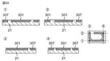
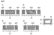
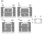
次に、本実施形態に係る積層型コイルアレイ1の製造方法について、図3A〜3Sを参照して以下に説明する。ただし、本実施形態に係る積層型コイルアレイ1の製造方法は、以下に説明する方法に限定されるものではない。なお、図3A〜3Sのそれぞれにおいて、右端の図は、各製造プロセスにおける積層体の上面図であり、残りの図はそれぞれ、上面図に示す破線1〜4に沿った断面図である。
[Manufacturing method of laminated coil array]
Next, a method for manufacturing the laminated coil array 1 according to the present embodiment will be described below with reference to FIGS. 3A to 3S. However, the method for manufacturing the laminated coil array 1 according to the present embodiment is not limited to the method described below. In each of FIGS. 3A to 3S, the rightmost view is a top view of the laminated body in each manufacturing process, and the remaining views are cross-sectional views taken along the broken lines 1 to 4 shown in the top view.
まず、以下に説明する手順で、内部に2つのコイル(第1コイル31および第2コイル32)が形成された、磁性層21を含む積層体を準備する。なお、図3A〜3Sにおいては、1つの積層型コイルアレイに対応する積層体を図示しているが、実際の製造方法においては、複数の積層型コイルアレイに対応する積層体を一体成型し、個片化することによって、複数の積層型コイルアレイを製造する。
First, a laminate including a
[磁性ペーストの調製]
磁性ペーストは、磁性層21を形成するのに用いられる。磁性ペーストは磁性材料を含む。磁性ペーストは、磁性材料に加えて、バインダー、溶剤および可塑剤等を含んでよい。
[Preparation of magnetic paste]
The magnetic paste is used to form the
(磁性材料)
磁性材料として、Fe、Co、Ni、およびこれらを含む合金等の金属磁性材料の粒子(金属磁性粒子)、またはフェライト粒子を用いることができる。磁性材料は、好ましくはFeまたはFe合金である。Fe合金としては、Fe−Si系合金、Fe−Si−Cr系合金、Fe−Si−Al系合金、Fe−Si−B−P−Cu−C系合金、Fe−Si−B−Nb−Cu系合金等が好ましい。上述の金属磁性材料からなる金属磁性粒子の表面は、絶縁被膜で覆われていることが好ましい。金属磁性粒子の表面が絶縁被膜で覆われていると、金属磁性粒子間の絶縁性を高くすることができる。絶縁被膜を形成する方法として、公知のゾル−ゲル法、メカノケミカル法等を用いることができる。絶縁被膜を構成する材料は、P、Si等の酸化物が好ましい。また、絶縁被膜は金属磁性粒子の表面が酸化されることで形成された酸化膜であってもよい。絶縁被膜の厚みは、好ましくは1nm以上50nm以下、より好ましくは1nm以上30nm以下、さらに好ましくは1nm以上20nm以下である。絶縁皮膜の厚みは、上述したように積層型コイルアレイの試料を研磨することで得られた断面を走査型電子顕微鏡(SEM)で撮影し、得られたSEM写真から、金属磁性粒子表面の絶縁被膜の厚みを測定することができる。
(Magnetic material)
As the magnetic material, particles of a metallic magnetic material (metal magnetic particles) such as Fe, Co, Ni, and an alloy containing these, or ferrite particles can be used. The magnetic material is preferably Fe or Fe alloy. Fe alloys include Fe—Si alloys, Fe—Si—Cr alloys, Fe—Si—Al alloys, Fe—Si—B—P—Cu—C alloys, and Fe—Si—B—Nb—Cu. A system alloy or the like is preferable. It is preferable that the surface of the metal magnetic particles made of the above-mentioned metal magnetic material is covered with an insulating film. When the surface of the metal magnetic particles is covered with an insulating film, the insulating property between the metal magnetic particles can be improved. As a method for forming the insulating film, a known sol-gel method, mechanochemical method or the like can be used. The material constituting the insulating film is preferably an oxide such as P or Si. Further, the insulating film may be an oxide film formed by oxidizing the surface of the metal magnetic particles. The thickness of the insulating film is preferably 1 nm or more and 50 nm or less, more preferably 1 nm or more and 30 nm or less, and further preferably 1 nm or more and 20 nm or less. As for the thickness of the insulating film, the cross section obtained by polishing the sample of the laminated coil array as described above is photographed with a scanning electron microscope (SEM), and the insulation of the surface of the metal magnetic particles is obtained from the obtained SEM photograph. The thickness of the coating can be measured.
金属磁性粒子の平均粒径は、好ましくは1μm以上30μm以下、より好ましくは1μm以上20μm以下、さらに好ましくは1μm以上10μm以下である。ここで、原料の金属磁性粒子の「平均粒径」は、体積基準のメジアン径(D50)を意味する。 The average particle size of the metal magnetic particles is preferably 1 μm or more and 30 μm or less, more preferably 1 μm or more and 20 μm or less, and further preferably 1 μm or more and 10 μm or less. Here, the "average particle size" of the raw material metal magnetic particles means a volume-based median diameter (D 50 ).
上述した金属磁性粒子に、ZnO粉末を、金属磁性粒子およびZnO粉末の重量の合計に対して0.2〜2重量%程度添加する。さらに、所定量のバインダー(エチルセルロース樹脂等)、溶剤(ターピネオール等)、可塑剤等を加えて混錬することにより、磁性ペーストを調製する。金属磁性粒子に所定量のZnO粉末を添加することにより、金属磁性粒子間の絶縁性をより高くすることができる。 To the above-mentioned metal magnetic particles, ZnO powder is added in an amount of about 0.2 to 2% by weight based on the total weight of the metal magnetic particles and the ZnO powder. Further, a magnetic paste is prepared by adding a predetermined amount of a binder (ethyl cellulose resin or the like), a solvent (terpineol or the like), a plasticizer or the like and kneading. By adding a predetermined amount of ZnO powder to the metal magnetic particles, the insulating property between the metal magnetic particles can be further improved.
[非磁性ペーストの調製]
非磁性ペーストは、非磁性層22および非磁性部23を形成するのに用いられる。非磁性ペーストは非磁性材料を含む。非磁性ペーストは、非磁性材料に加えて、バインダー、溶剤および可塑剤等を含んでよい。
[Preparation of non-magnetic paste]
The non-magnetic paste is used to form the
(非磁性材料)
非磁性材料として、ガラスセラミック材料および非磁性フェライト材料等を用いることができるが、非磁性フェライト材料を用いることが好ましい。非磁性フェライト材料としては、FeがFe2O3に換算して40mol%以上49.5mol%以下、CuがCuOに換算して6mol%以上12mol%以下、残部がZnOである組成を有する非磁性フェライト材料を用いることができる。非磁性材料は、必要に応じて添加物としてMn3O4、Co3O4、SnO2、Bi2O3およびSiO2等が添加されていてよく、微量な不可避不純物を含有していてもよい。
(Non-magnetic material)
As the non-magnetic material, a glass ceramic material, a non-magnetic ferrite material, or the like can be used, but it is preferable to use a non-magnetic ferrite material. The non-magnetic ferrite material has a composition in which Fe is 40 mol% or more and 49.5 mol% or less in terms of Fe 2 O 3 , Cu is 6 mol % or more and 12 mol% or less in terms of CuO, and the balance is ZnO. A magnetic ferrite material can be used. The non-magnetic material may contain Mn 3 O 4 , Co 3 O 4 , SnO 2 , Bi 2 O 3 and SiO 2 as additives as necessary, even if it contains a trace amount of unavoidable impurities. good.
Fe2O3、ZnO、CuO等を所定の比率になるように秤量し、湿式で混合および粉砕した後、乾燥させる。得られた乾燥物を700℃以上800℃以下の温度で仮焼して、非磁性フェライト材料の粉末を調製する。この非磁性フェライト材料に、所定量の溶剤(ケトン系溶剤等)、バインダー(ポリビニルアセタール樹脂等)、および可塑剤(アルキド系可塑剤等)を加えて混錬することにより、非磁性ペーストを調製する。 Fe 2 O 3 , ZnO, CuO, etc. are weighed to a predetermined ratio, mixed and pulverized in a wet manner, and then dried. The obtained dried product is calcined at a temperature of 700 ° C. or higher and 800 ° C. or lower to prepare a powder of a non-magnetic ferrite material. A non-magnetic paste is prepared by adding a predetermined amount of solvent (ketone solvent, etc.), binder (polyvinyl acetal resin, etc.), and plasticizer (alkyd-based plasticizer, etc.) to this non-magnetic ferrite material and kneading. do.
[導電性ペーストの調製]
導電性ペーストは、第1コイル31および第2コイル32ならびに第1〜第4外部電極401〜404を形成するのに用いられる。導電性ペーストは、Ag粉末等の導電性材料を含む。導電性ペーストは、導電性材料に加えて、溶剤、樹脂および分散剤等を含んでよい。
[Preparation of conductive paste]
The conductive paste is used to form the
Ag粉末を準備し、所定量の溶剤(オイゲノール(4−アリル−2−メトキシフェノール)等)、樹脂(エチルセルロース等)、および分散剤を加えて混錬することにより、導電性ペーストを調製する。ここで、Ag粉末の平均粒径(体積基準のメジアン径D50)は、1μm以上10μm以下であることが好ましい。第1コイル31および第2コイル32ならびに第1〜第4外部電極401〜404は、同じ導電性ペーストを用いて形成してよいが、異なる組成を有する導電性ペーストを用いて形成してもよい。
A conductive paste is prepared by preparing Ag powder, adding a predetermined amount of solvent (eugenol (4-allyl-2-methoxyphenol), etc.), resin (ethyl cellulose, etc.), and a dispersant and kneading. Here, the average particle size of the Ag powder (volume-based median diameter D 50 ) is preferably 1 μm or more and 10 μm or less. The
[素体2の作製]
金属プレートの上に熱剥離シートおよびPET(ポリエチレンテレフタレート)フィルムを積み重ね、その上に、磁性ペーストを印刷して乾燥させる。磁性ペーストの厚みが所定の厚みになるように印刷および乾燥を繰り返し、積層型コイルアレイの上面側の磁性層21を形成する。
[Preparation of element body 2]
A heat release sheet and a PET (polyethylene terephthalate) film are stacked on a metal plate, and a magnetic paste is printed on the metal plate and dried. Printing and drying are repeated so that the thickness of the magnetic paste becomes a predetermined thickness, and the
上述した磁性層21の上に、導電性ペーストを印刷して、第1コイル31を構成する第1のコイル導体301を形成する。このとき、第1のコイル導体301の外側の所定位置に導電性ペーストを印刷して、コイルの終端を底面に引き出すための接続部307も形成する。印刷した導電性ペーストを乾燥させた後、第1のコイル導体301および接続部307の周囲に磁性ペーストを印刷して充填し、乾燥させる。第1のコイル導体301およびその周囲の磁性層21が所定の厚みになるように、導電性ペーストおよび磁性ペーストの印刷および乾燥を繰り返し、磁性層21が周囲に充填された第1のコイル導体301を形成する(図3A)。図3Aに示す例においては、導電性ペーストおよび磁性ペーストの印刷および乾燥を2回繰り返している。
A conductive paste is printed on the
なお、図3Aに示す工程で形成した接続部はコイルの終端と外部電極との接続に直接寄与しないが、図3Aに示す接続部を形成した場合、素体2の内部においてほぼ対称な位置に接続部が設けられることとなるので、素体2の各部分における収縮率の差を小さくすることができる。
The connection portion formed in the step shown in FIG. 3A does not directly contribute to the connection between the end of the coil and the external electrode, but when the connection portion shown in FIG. 3A is formed, the positions are substantially symmetrical inside the
次に、第1のコイル導体301の上に、第1コイル31を構成する第2のコイル導体302と接続するための接続層308を形成する領域を残して、非磁性ペーストを印刷して非磁性部23を形成する。次いで、非磁性ペーストを印刷しなかった上述の領域に導電性ペーストを印刷して接続層308を形成する。また、接続部307を形成する位置にも導電性ペーストを印刷する。このように形成した非磁性部23、接続層308および接続部307の周囲に磁性ペーストを印刷して充填し、乾燥させる。接続層308が所定の厚みになるように、上述の手順を繰り返す(図3B)。
Next, a non-magnetic paste is printed on the
上述した手順と同様の手順で、第1コイル31を構成するコイル導体をn層、隣り合うコイル導体を連結する接続層308をn−1層、繰り返し積層する(nは2以上の整数)。図3A〜3Sに示す製造例においては、上述した非磁性部の上に導電性ペーストを印刷して、第2のコイル導体302を形成する。このとき、第2のコイル導体302の終端は接続層308まで延在し、接続層308を介して第1のコイル導体301と接続する。また同時に、接続部307を形成する位置にも導電性ペーストを印刷する。次に、第2のコイル導体302の始端と終端との間に非磁性ペーストを印刷して非磁性部23を形成する。第2のコイル導体302、接続部307および非磁性部23の周囲に磁性ペーストを印刷して充填し、乾燥させる。第2のコイル導体302が所定の厚みになるように、上述の手順を繰り返し、磁性層21が周囲に充填された第2のコイル導体302を形成する(図3C)。
In the same procedure as described above, n layers of coil conductors constituting the
次に、第2のコイル導体302の上に、第1コイル31を構成する第3のコイル導体303と接続するための接続層308を形成する領域を残して、非磁性ペーストを印刷して非磁性部23を形成する。ついで、非磁性ペーストを印刷しなかった上述の領域に導電性ペーストを印刷して接続層308を形成する。また、接続部307を形成する位置にも導電性ペーストを印刷する。このように形成した非磁性部23、接続層308および接続部307の周囲に磁性ペーストを印刷して充填し、乾燥させる。接続層308が所定の厚みになるように、上述の手順を繰り返す(図3D)。
Next, a non-magnetic paste is printed on the
次に、非磁性部23の上に導電性ペーストを印刷して、第3のコイル導体303を形成する。このとき、第3のコイル導体303の終端は接続層308まで延在し、接続層308を介して第2のコイル導体302と接続する。また同時に、接続部307を形成する位置にも導電性ペーストを印刷する。第3のコイル導体303および接続部307の周囲に磁性ペーストを印刷して充填し、乾燥させる。第3のコイル導体303が所定の厚みになるように、上述の手順を繰り返す(図3E)。このとき、図3Fに示すように、第3のコイル導体303を構成するコイル導体層のうち、最後に印刷するコイル導体層(すなわち、非磁性層22に接するコイル導体層)の長さを、他のコイル導体層の長さと異なる長さにしてよい。図3A〜3Sに示す製造例においては、最後に印刷するコイル導体層の長さを、他のコイル導体層の長さより短くしている。このようにして、磁性層21が周囲に充填された第3のコイル導体303を形成する。
Next, the conductive paste is printed on the
上述の手順により、第1〜第3のコイル導体301〜303が接続層308を介して連結してなる第1コイル31が形成される。なお、図3A〜3Sに示す製造例において、第1コイルのターン数は2.5であるが、本発明に係る積層型コイルアレイはこれに限定されるものではなく、ターン数は必要に応じて適宜変更してよい。
By the above procedure, the
次に、接続部307を形成する位置に導電性ペーストを印刷し、その周囲に非磁性ペーストを印刷して、非磁性層22を形成する(図3G)。非磁性層22が所定の厚みになるように、導電性ペーストおよび非磁性ペーストの印刷および乾燥を繰り返す。
Next, the conductive paste is printed at the position where the
次に、第2コイル32を以下に説明する手順で形成する。まず、非磁性層22の上に導電性ペーストを印刷して、第2コイル32を構成する第4のコイル導体304を形成する。また、接続部307を形成する位置にも導電性ペーストを印刷する。第4のコイル導体304および接続部307の周囲に磁性ペーストを印刷して充填し、乾燥させる。第4のコイル導体304が所定の厚みになるように、上述の手順を繰り返す(図3Hおよび3I)。このとき、図3Hに示すように、第4のコイル導体304を構成するコイル導体層のうち、最初に印刷するコイル導体層(すなわち、非磁性層22に接するコイル導体層)の長さを、他のコイル導体層の長さと異なる長さにしてよい。図3A〜3Sに示す製造例においては、最初に印刷するコイル導体層の長さを、他のコイル導体層の長さより短くしている。このようにして、磁性層21が周囲に充填された第4のコイル導体304を形成する。
Next, the
なお、図3A〜3Sに示す製造例においては、第1コイル31を構成するコイル導体層、および第2コイル32を構成するコイル導体層の両方の長さを、他のコイル導体層の長さと異なる長さにしているが、この構成は必須ではなく、第1コイル31を構成するコイル導体層および第2コイル32を構成するコイル導体層の少なくとも一方の長さが、他のコイル導体層の長さと異なっていればよい。
In the manufacturing examples shown in FIGS. 3A to 3S, the lengths of both the coil conductor layer constituting the
次に、第4のコイル導体304の上に、第2コイル32を構成する第5のコイル導体305と接続するための接続層308を形成する領域を残して、非磁性ペーストを印刷して非磁性部23を形成する。ついで、非磁性ペーストを印刷しなかった上述の領域に導電性ペーストを印刷して接続層308を形成する。また、接続部307を形成する位置にも導電性ペーストを印刷する。このように形成した非磁性部23、接続層308および接続部307の周囲に磁性ペーストを印刷して充填し、乾燥させる。接続層308が所定の厚みになるように、上述の手順を繰り返す(図3J)。
Next, a non-magnetic paste is printed on the
次に、非磁性部23の上に導電性ペーストを印刷して、第5のコイル導体305を形成する。このとき、第5のコイル導体305の終端は接続層308まで延在し、接続層308を介して第4のコイル導体304と接続する。また同時に、接続部307を形成する位置にも導電性ペーストを印刷する。第5のコイル導体305および接続部307の周囲に磁性ペーストを印刷して充填し、乾燥させる。第5のコイル導体305が所定の厚みになるように、上述の手順を繰り返す(図3K)。このようにして、磁性層21が周囲に充填された第5のコイル導体305を形成する。
Next, the conductive paste is printed on the
次に、第5のコイル導体305の上に、第2コイル32を構成する第6のコイル導体306と接続するための接続層308を形成する領域を残して、非磁性ペーストを印刷して非磁性部23を形成する。ついで、非磁性ペーストを印刷しなかった上述の領域に導電性ペーストを印刷して接続層308を形成する。また、接続部307を形成する位置にも導電性ペーストを印刷する。このように形成した非磁性部23、接続層308および接続部307の周囲に磁性ペーストを印刷して充填し、乾燥させる。接続層308が所定の厚みになるように、上述の手順を繰り返す(図3L)。
Next, a non-magnetic paste is printed on the
次に、非磁性部23の上に導電性ペーストを印刷して、第6のコイル導体306を形成する。このとき、第6のコイル導体306の終端は接続層308まで延在し、接続層308を介して第5のコイル導体305と接続する。また同時に、接続部307を形成する位置にも導電性ペーストを印刷する。第6のコイル導体306および接続部307の周囲に磁性ペーストを印刷して充填し、乾燥させる。第6のコイル導体306が所定の厚みになるように、上述の手順を繰り返す(図3M)。このようにして、磁性層21が周囲に充填された第6のコイル導体306を形成する。
Next, the conductive paste is printed on the
上述の手順により、第4〜第6のコイル導体304〜306が接続層308を介して連結してなる第2コイル32が形成される。なお、図3A〜3Sに示す製造例において、第2コイル32のターン数は2.5であるが、本発明に係る積層型コイルアレイはこれに限定されるものではなく、ターン数は必要に応じて適宜変更してよい。
By the above procedure, the
上述の手順により所定数のコイル導体を形成した後、第1コイル31および第2コイル32の始端および終端を素体2の底面に引き出して外部電極に接続する接続部307を形成する。接続部307を形成する位置に導電性ペーストを印刷し、乾燥させる。接続部307の周囲に磁性ペーストを印刷して充填し、乾燥させる。接続部307が所定の厚みになるように、導電性ペーストおよび磁性ペーストの印刷および乾燥を繰り返す(図3N)。このようにして接続部307を形成する際、接続部307の周囲に印刷する磁性ペーストの複数の層のうち、いずれかの層について、磁性ペーストの代わりに非磁性ペーストを印刷して追加の非磁性層を形成してもよい。この追加の非磁性層は、1層以上存在してよい。コイルと外部電極との間に追加の非磁性層を設けることで、コイルと外部電極間の絶縁性を高めることができる。
After forming a predetermined number of coil conductors by the above procedure, the start and end ends of the
一の変形例において、図3Rに示すように、追加の非磁性層24は、外部電極に対向するコイル導体に接してよい。外部電極に対向するコイル導体と、追加の非磁性層とが接していると、積層型コイルアレイ1の直流重畳特性をより一層向上させることができる。
In one modification, as shown in FIG. 3R, the additional
別の変形例において、図3Sに示すように、追加の非磁性層24は、外部電極に接してよい。追加の非磁性層を外部電極に接するように設けることで、外部電極間の直流抵抗を向上させることができる。
In another modification, as shown in FIG. 3S, the additional
もう1つの変形例において、追加の非磁性層は、外部電極に対向するコイル導体に接する位置と、外部電極に接する位置の中間の位置に設けてもよい。このような位置に追加の非磁性層を設けることにより、直流重畳特性の向上と、外部電極間の直流抵抗の向上とをバランスよく達成することができる。 In another modification, the additional non-magnetic layer may be provided at a position intermediate between the position in contact with the coil conductor facing the external electrode and the position in contact with the external electrode. By providing the additional non-magnetic layer at such a position, it is possible to achieve both the improvement of the DC superimposition characteristic and the improvement of the DC resistance between the external electrodes in a well-balanced manner.
以上の手順により、内部にコイルが形成された、磁性層を含む積層体を準備する。 By the above procedure, a laminated body including a magnetic layer having a coil formed inside is prepared.
次いで、外部電極を形成する。まず、上述の手順により得られた積層体の表面に導電性ペーストを塗布して、第1外部電極401、第2外部電極402、第3外部電極403、および第4外部電極404を構成する第1外部電極層を形成する(図3O)。なお、外部電極を形成する積層体の表面は、素体の底面に相当する面である。積層体の表面に露出した接続部307をそれぞれ覆うように導電性ペーストを印刷して、4つの外部電極パターンを形成し、乾燥させる。
Next, an external electrode is formed. First, a conductive paste is applied to the surface of the laminate obtained by the above procedure to form a first
次に、磁性ペーストまたは非磁性ペーストを、第1外部電極層の外縁部の少なくとも一部と重なるように塗布して、磁性ペースト層または非磁性ペースト層を形成する(図3P)。このとき、磁性ペーストまたは非磁性ペーストは、第1外部電極層の周囲を充填するように印刷して乾燥させる。なお、図3Pに示す例においては、磁性ペースト層が形成されている。このように磁性ペーストまたは非磁性ペーストを塗布することにより、素体と外部電極との密着性を向上させることができる。 Next, the magnetic paste or the non-magnetic paste is applied so as to overlap with at least a part of the outer edge portion of the first external electrode layer to form the magnetic paste layer or the non-magnetic paste layer (FIG. 3P). At this time, the magnetic paste or the non-magnetic paste is printed so as to fill the periphery of the first external electrode layer and dried. In the example shown in FIG. 3P, a magnetic paste layer is formed. By applying the magnetic paste or the non-magnetic paste in this way, the adhesion between the element body and the external electrode can be improved.
次に、導電性ペーストを第1外部電極層の上に塗布して、第1〜第4外部電極401〜404を構成する第2外部電極層を形成する。第2外部電極層は、第2外部電極層の一部が、磁性ペースト層または非磁性ペースト層の外縁部の少なくとも一部と重なるように形成される(図3Q)。このように第1〜第4外部電極401〜404を形成することにより、外部電極と素体との密着性を向上させることができる。また、第2外部電極層を積層体の最外層とすることにより、得られる積層型コイルアレイの素体の底面において、外部電極の最外面が素体の底面よりも外側に存在することになる。その結果、得られる積層型コイルアレイにおいて、素体と外部電極との密着性の向上と、実装時のコンタクト性の向上とを両立することができる。
Next, the conductive paste is applied on the first external electrode layer to form the second external electrode layer constituting the first to fourth
なお、図3A〜図3Sに示す製造例においては、第1〜第4外部電極401〜404は、2つの外部電極層(第1外部電極層および第2外部電極層)を積層することにより形成されているが、本発明に係る積層型コイルアレイおよびその製造方法は、このような形態に限定されるものではなく、3層以上の外部電極層を積層して外部電極を形成してもよい。外部電極層をn層積層する場合(nは3以上の整数)、上述した導電性ペーストおよび磁性ペーストまたは非磁性ペーストの印刷および乾燥をn−1回繰り返した後、最後に導電性ペーストを印刷し、乾燥させて、第n外部電極層を形成する。このように、積層体の最外層が外部電極層となるように積層を行うことにより、得られる積層型コイルアレイにおいて、外部電極の最外面が素体の底面よりも外側に存在することになる。
In the production examples shown in FIGS. 3A to 3S, the first to fourth
このようにして得られた積層体を加熱することにより金属プレートから剥離し、圧着した後、積層体からPETフィルムを剥離する。このようにして、素体の集合体である積層体が得られる。 The laminate thus obtained is peeled off from the metal plate by heating, pressure-bonded, and then the PET film is peeled off from the laminate. In this way, a laminated body which is an aggregate of elementary bodies is obtained.
次いで、得られた積層体をダイサー等で切断して個片化する。個片化した積層体をバレル処理して、積層体の角部に丸みをつける。なお、バレル処理は積層体を焼成する前に行ってよく、あるいは、焼成後の素体にバレル処理を施してもよい。バレル処理の方法は、乾式または湿式のいずれであってもよく、あるいは、積層体同士を共擦する方法や、メディアと一緒にバレル処理する方法であってもよい。 Next, the obtained laminate is cut with a dicer or the like to be individualized. The individualized laminate is barrel-treated to round the corners of the laminate. The barrel treatment may be performed before the laminated body is fired, or the element body after firing may be subjected to the barrel treatment. The method of barrel treatment may be either dry or wet, or may be a method of co-rubbing the laminates together or a method of barreling with media.
次に、バレル処理を施した積層体を焼成する。積層体を焼成炉に入れて、650℃以上750℃以下の温度で焼成を行って、外部電極が底面に設けられた素体を得る。焼成後の素体を、1Pa以下の真空環境下で樹脂(エポキシ樹脂等)に浸漬し、素体の内部に樹脂を含浸させる。樹脂を含浸させた後の素体を、溶剤(ブチルカルビトールアセテート(2−(2−ブトキシエトキシ)エチルアセタート)等)で洗浄し、自然乾燥した後、100℃以上200℃以下の温度で樹脂を硬化させる。その後、素体の表面に形成された外部電極(下地電極)の上に、無電解めっきによりNiめっき層およびSnめっき層を形成する。このようにして、図1Aおよび図1Bに示す積層型コイルアレイ1が得られる。 Next, the barrel-treated laminate is fired. The laminate is placed in a firing furnace and fired at a temperature of 650 ° C. or higher and 750 ° C. or lower to obtain a body having an external electrode provided on the bottom surface. The element body after firing is immersed in a resin (epoxy resin or the like) in a vacuum environment of 1 Pa or less, and the inside of the element body is impregnated with the resin. After impregnating with the resin, the element body is washed with a solvent (butyl carbitol acetate (2- (2-butoxyethoxy) ethyl acetate), etc.), air-dried, and then at a temperature of 100 ° C. or higher and 200 ° C. or lower. Cure the resin. Then, a Ni plating layer and a Sn plating layer are formed by electroless plating on an external electrode (base electrode) formed on the surface of the element body. In this way, the laminated coil array 1 shown in FIGS. 1A and 1B is obtained.
以上、素体内に2つのコイルが内蔵された積層型コイルアレイの製造方法について説明したが、本実施形態に係る積層型コイルアレイは3以上のコイルを備えてもよく、この場合においても、上述した方法と同様の手順により積層型コイルアレイを製造することができる。また、本実施形態に係る積層型コイルアレイにおいて、第1コイル31および第2コイル32はそれぞれ、3つのコイル導体が連結されてなるものであったが、各コイルは、2つのコイル導体、または4以上のコイル導体で構成されてもよい。
Although the method for manufacturing a laminated coil array in which two coils are built in the element body has been described above, the laminated coil array according to the present embodiment may include three or more coils, and even in this case, the above description is also given. The laminated coil array can be manufactured by the same procedure as the above method. Further, in the laminated coil array according to the present embodiment, the
本発明は以下の態様を含むが、これらの態様に限定されるものではない。
(態様1)
磁性粒子を含有する磁性層を含む素体と、
素体に内蔵された第1コイルおよび第2コイルと、
素体の表面に設けられ、第1コイルおよび第2コイルの端部のいずれか1つにそれぞれ電気的に接続された第1外部電極、第2外部電極、第3外部電極および第4外部電極と
を有してなる積層型コイルアレイであって、
第1コイルと第2コイルとの間に非磁性層が設けられており、
第1コイルおよび第2コイルはそれぞれ、複数のコイル導体が積層方向に連結されてなり、
第1コイルの複数のコイル導体のうち最も第2コイルに近いコイル導体、および第2コイルの複数のコイル導体のうち最も第1コイルに近いコイル導体の少なくとも一方が、非磁性層に接しており、
非磁性層に接しているコイル導体を構成するコイル導体層のうち、前記非磁性層に接しているコイル導体層の長さは、他のコイル導体層の長さと異なる、積層型コイルアレイ。
The present invention includes, but is not limited to, the following aspects.
(Aspect 1)
An element body containing a magnetic layer containing magnetic particles,
The first coil and the second coil built in the element body,
A first external electrode, a second external electrode, a third external electrode, and a fourth external electrode provided on the surface of the element body and electrically connected to any one of the ends of the first coil and the second coil, respectively. It is a laminated coil array having and
A non-magnetic layer is provided between the first coil and the second coil.
Each of the first coil and the second coil is formed by connecting a plurality of coil conductors in the stacking direction.
At least one of the coil conductor closest to the second coil among the plurality of coil conductors of the first coil and the coil conductor closest to the first coil among the plurality of coil conductors of the second coil are in contact with the non-magnetic layer. ,
A laminated coil array in which the length of the coil conductor layer in contact with the non-magnetic layer is different from the length of other coil conductor layers among the coil conductor layers constituting the coil conductor in contact with the non-magnetic layer.
(態様2)
非磁性層に接しているコイル導体を構成するコイル導体層のうち、前記非磁性層に接しているコイル導体層の長さは、他のコイル導体層の長さよりも短い、態様1に記載の積層型コイルアレイ。
(Aspect 2)
The first aspect of the embodiment, wherein among the coil conductor layers constituting the coil conductor in contact with the non-magnetic layer, the length of the coil conductor layer in contact with the non-magnetic layer is shorter than the length of the other coil conductor layers. Stacked coil array.
(態様3)
第1コイルの複数のコイル導体、および第2コイルの複数のコイル導体のうち隣接するコイル導体間の少なくとも1か所に非磁性部が設けられている、態様1または2に記載の積層型コイルアレイ。
(Aspect 3)
The laminated coil according to
(態様4)
非磁性層および非磁性部は同じ組成を有する、態様3に記載の積層型コイルアレイ。
(Aspect 4)
The laminated coil array according to
(態様5)
非磁性層および非磁性部は、Zn−Cu系フェライトで構成される、態様4に記載の積層型コイルアレイ。
(Aspect 5)
The laminated coil array according to
本発明に係る積層型コイルアレイは、DC−DCコンバータ等の幅広い用途に用いることができる。 The laminated coil array according to the present invention can be used in a wide range of applications such as DC-DC converters.
1 積層型コイルアレイ
2 素体
31 第1コイル
32 第2コイル
301 第1のコイル導体
302 第2のコイル導体
303 第3のコイル導体
304 第4のコイル導体
305 第5のコイル導体
306 第6のコイル導体
307 接続部
308 接続層
309 コイル導体層
401 第1外部電極
402 第2外部電極
403 第3外部電極
404 第4外部電極
21 磁性層
22 非磁性層
23 非磁性部
24 追加の非磁性層
1 Laminated
Claims (6)
前記素体に内蔵された第1コイルおよび第2コイルと、
前記素体の表面に設けられ、前記第1コイルおよび前記第2コイルの端部のいずれか1つにそれぞれ電気的に接続された第1外部電極、第2外部電極、第3外部電極および第4外部電極と
を有してなる積層型コイルアレイであって、
前記第1コイルと前記第2コイルとの間に非磁性層が設けられており、
前記第1コイルおよび前記第2コイルはそれぞれ、複数のコイル導体が積層方向に連結されてなり、
前記第1コイルの前記複数のコイル導体のうち最も前記第2コイルに近いコイル導体、および前記第2コイルの前記複数のコイル導体のうち最も前記第1コイルに近いコイル導体の少なくとも一方が、前記非磁性層に接しており、
前記非磁性層に接しているコイル導体を構成するコイル導体層のうち、前記非磁性層に接しているコイル導体層の長さは、他のコイル導体層の長さと異なっており、
前記非磁性層に接しているコイル導体層の両端を巻回方向に沿うように繋いだ位置には、前記磁性層が設けられている、積層型コイルアレイ。 An element body containing a magnetic layer containing magnetic particles,
The first coil and the second coil built in the element body,
A first external electrode, a second external electrode, a third external electrode, and a first external electrode provided on the surface of the element body and electrically connected to any one of the ends of the first coil and the second coil, respectively. A laminated coil array having 4 external electrodes.
A non-magnetic layer is provided between the first coil and the second coil.
The first coil and the second coil each have a plurality of coil conductors connected in the stacking direction.
At least one of the coil conductor closest to the second coil among the plurality of coil conductors of the first coil and the coil conductor closest to the first coil among the plurality of coil conductors of the second coil is said. It is in contact with the non-magnetic layer and
Wherein among the coil conductor layer constituting the coil conductor in contact with the nonmagnetic layer, wherein the length of the coil conductor layer in contact with the nonmagnetic layer is Tsu and Do different lengths of the other coil conductor layer,
A laminated coil array in which the magnetic layer is provided at a position where both ends of the coil conductor layer in contact with the non-magnetic layer are connected along the winding direction.
Priority Applications (3)
| Application Number | Priority Date | Filing Date | Title |
|---|---|---|---|
| JP2018190195A JP6977694B2 (en) | 2018-10-05 | 2018-10-05 | Laminated coil array |
| CN201910923223.8A CN111009394B (en) | 2018-10-05 | 2019-09-27 | Laminated Coil Array |
| US16/592,596 US11783999B2 (en) | 2018-10-05 | 2019-10-03 | Multilayer coil array |
Applications Claiming Priority (1)
| Application Number | Priority Date | Filing Date | Title |
|---|---|---|---|
| JP2018190195A JP6977694B2 (en) | 2018-10-05 | 2018-10-05 | Laminated coil array |
Publications (3)
| Publication Number | Publication Date |
|---|---|
| JP2020061411A JP2020061411A (en) | 2020-04-16 |
| JP2020061411A5 JP2020061411A5 (en) | 2020-07-02 |
| JP6977694B2 true JP6977694B2 (en) | 2021-12-08 |
Family
ID=70051230
Family Applications (1)
| Application Number | Title | Priority Date | Filing Date |
|---|---|---|---|
| JP2018190195A Active JP6977694B2 (en) | 2018-10-05 | 2018-10-05 | Laminated coil array |
Country Status (3)
| Country | Link |
|---|---|
| US (1) | US11783999B2 (en) |
| JP (1) | JP6977694B2 (en) |
| CN (1) | CN111009394B (en) |
Families Citing this family (5)
| Publication number | Priority date | Publication date | Assignee | Title |
|---|---|---|---|---|
| JP6981389B2 (en) * | 2018-10-05 | 2021-12-15 | 株式会社村田製作所 | Stacked coil array for DC-DC converter and DC-DC converter |
| JP6977694B2 (en) | 2018-10-05 | 2021-12-08 | 株式会社村田製作所 | Laminated coil array |
| JP7074050B2 (en) * | 2018-12-28 | 2022-05-24 | 株式会社村田製作所 | Coil parts |
| KR102198532B1 (en) * | 2019-06-25 | 2021-01-06 | 삼성전기주식회사 | Coil component |
| WO2024161683A1 (en) * | 2023-01-30 | 2024-08-08 | 株式会社村田製作所 | Layered coil and layered coil array |
Family Cites Families (21)
| Publication number | Priority date | Publication date | Assignee | Title |
|---|---|---|---|---|
| JP2001110638A (en) * | 1999-10-14 | 2001-04-20 | Tdk Corp | Laminate electronic component |
| US8416043B2 (en) | 2010-05-24 | 2013-04-09 | Volterra Semiconductor Corporation | Powder core material coupled inductors and associated methods |
| JP2005129793A (en) * | 2003-10-24 | 2005-05-19 | Murata Mfg Co Ltd | Method for manufacturing laminated ceramic electronic component |
| JP2006351954A (en) * | 2005-06-17 | 2006-12-28 | Tdk Corp | Stacked common mode filter |
| JP2007281315A (en) * | 2006-04-11 | 2007-10-25 | Hitachi Metals Ltd | Coil component |
| JP5626834B2 (en) * | 2008-01-08 | 2014-11-19 | 株式会社村田製作所 | Manufacturing method of open magnetic circuit type multilayer coil parts |
| JP2012160506A (en) * | 2011-01-31 | 2012-08-23 | Toko Inc | Laminated type inductor |
| JP5786647B2 (en) | 2011-10-28 | 2015-09-30 | 株式会社村田製作所 | Multilayer substrate and DC-DC converter |
| JP2015073052A (en) * | 2013-10-04 | 2015-04-16 | 株式会社村田製作所 | Inductor array and power supply device |
| KR20160032581A (en) | 2014-09-16 | 2016-03-24 | 삼성전기주식회사 | Inductor array chip and board for mounting the same |
| JP6252425B2 (en) * | 2014-10-03 | 2017-12-27 | 株式会社村田製作所 | Electronic components |
| JP6460329B2 (en) | 2015-02-27 | 2019-01-30 | 株式会社オートネットワーク技術研究所 | Reactor |
| JP6380192B2 (en) | 2015-03-27 | 2018-08-29 | 株式会社村田製作所 | Multilayer electronic components |
| JP6565555B2 (en) * | 2015-09-30 | 2019-08-28 | Tdk株式会社 | Multilayer common mode filter |
| JP6493617B2 (en) * | 2016-02-16 | 2019-04-03 | 株式会社村田製作所 | Voltage detection device, power supply device, and power transmission device |
| JP6812140B2 (en) | 2016-05-30 | 2021-01-13 | 株式会社村田製作所 | Coil parts |
| KR102632343B1 (en) | 2016-08-26 | 2024-02-02 | 삼성전기주식회사 | Inductor array component and board for mounting the same |
| JP7188869B2 (en) * | 2017-03-31 | 2022-12-13 | 太陽誘電株式会社 | common mode choke coil |
| JP7065720B2 (en) | 2018-07-19 | 2022-05-12 | 太陽誘電株式会社 | Magnetically coupled coil parts and their manufacturing methods |
| JP6977694B2 (en) | 2018-10-05 | 2021-12-08 | 株式会社村田製作所 | Laminated coil array |
| US11094455B2 (en) | 2018-12-27 | 2021-08-17 | Texas Instruments Incorporated | Module with reversely coupled inductors and magnetic molded compound (MMC) |
-
2018
- 2018-10-05 JP JP2018190195A patent/JP6977694B2/en active Active
-
2019
- 2019-09-27 CN CN201910923223.8A patent/CN111009394B/en active Active
- 2019-10-03 US US16/592,596 patent/US11783999B2/en active Active
Also Published As
| Publication number | Publication date |
|---|---|
| CN111009394A (en) | 2020-04-14 |
| CN111009394B (en) | 2023-09-01 |
| JP2020061411A (en) | 2020-04-16 |
| US20200111609A1 (en) | 2020-04-09 |
| US11783999B2 (en) | 2023-10-10 |
Similar Documents
| Publication | Publication Date | Title |
|---|---|---|
| JP6977694B2 (en) | Laminated coil array | |
| KR101954579B1 (en) | Laminated inductor | |
| JP7235088B2 (en) | Multilayer electronic component | |
| JP2018098278A (en) | Coil component | |
| US8779884B2 (en) | Multilayered inductor and method of manufacturing the same | |
| US8400251B2 (en) | Electronic component and method for manufacturing the same | |
| JP7032039B2 (en) | Multilayer coil parts | |
| JP6919641B2 (en) | Laminated electronic components | |
| US20220102062A1 (en) | Electronic component and method of manufacturing the same | |
| KR20080101771A (en) | Ferrite pastes, and production method of multilayer ceramic device | |
| CN112582130B (en) | Coil component | |
| JP7221583B2 (en) | coil parts | |
| JP6981389B2 (en) | Stacked coil array for DC-DC converter and DC-DC converter | |
| JP2022137227A (en) | Coil component | |
| US20190311847A1 (en) | Coil component | |
| JP2023148899A (en) | Coil component | |
| JP2023103954A (en) | Coil component | |
| JP2023103827A (en) | Coil component | |
| JP2023148896A (en) | Coil component |
Legal Events
| Date | Code | Title | Description |
|---|---|---|---|
| A521 | Request for written amendment filed |
Free format text: JAPANESE INTERMEDIATE CODE: A523 Effective date: 20200430 |
|
| A621 | Written request for application examination |
Free format text: JAPANESE INTERMEDIATE CODE: A621 Effective date: 20200430 |
|
| A977 | Report on retrieval |
Free format text: JAPANESE INTERMEDIATE CODE: A971007 Effective date: 20210310 |
|
| A131 | Notification of reasons for refusal |
Free format text: JAPANESE INTERMEDIATE CODE: A131 Effective date: 20210323 |
|
| A601 | Written request for extension of time |
Free format text: JAPANESE INTERMEDIATE CODE: A601 Effective date: 20210517 |
|
| A521 | Request for written amendment filed |
Free format text: JAPANESE INTERMEDIATE CODE: A523 Effective date: 20210712 |
|
| TRDD | Decision of grant or rejection written | ||
| A01 | Written decision to grant a patent or to grant a registration (utility model) |
Free format text: JAPANESE INTERMEDIATE CODE: A01 Effective date: 20211012 |
|
| A61 | First payment of annual fees (during grant procedure) |
Free format text: JAPANESE INTERMEDIATE CODE: A61 Effective date: 20211025 |
|
| R150 | Certificate of patent or registration of utility model |
Ref document number: 6977694 Country of ref document: JP Free format text: JAPANESE INTERMEDIATE CODE: R150 |