JP6207713B2 - Display device - Google Patents
Display device Download PDFInfo
- Publication number
- JP6207713B2 JP6207713B2 JP2016246484A JP2016246484A JP6207713B2 JP 6207713 B2 JP6207713 B2 JP 6207713B2 JP 2016246484 A JP2016246484 A JP 2016246484A JP 2016246484 A JP2016246484 A JP 2016246484A JP 6207713 B2 JP6207713 B2 JP 6207713B2
- Authority
- JP
- Japan
- Prior art keywords
- electrode
- region
- thin film
- film transistor
- semiconductor film
- Prior art date
- Legal status (The legal status is an assumption and is not a legal conclusion. Google has not performed a legal analysis and makes no representation as to the accuracy of the status listed.)
- Active
Links
- 239000004065 semiconductor Substances 0.000 claims description 235
- 239000003990 capacitor Substances 0.000 claims description 62
- 239000000463 material Substances 0.000 claims description 20
- 229910052710 silicon Inorganic materials 0.000 claims description 20
- 239000010703 silicon Substances 0.000 claims description 20
- 239000010408 film Substances 0.000 description 265
- 239000010409 thin film Substances 0.000 description 155
- 239000012535 impurity Substances 0.000 description 55
- IJGRMHOSHXDMSA-UHFFFAOYSA-N Atomic nitrogen Chemical compound N#N IJGRMHOSHXDMSA-UHFFFAOYSA-N 0.000 description 54
- 230000003071 parasitic effect Effects 0.000 description 45
- 239000007789 gas Substances 0.000 description 37
- 239000004973 liquid crystal related substance Substances 0.000 description 34
- 229910052757 nitrogen Inorganic materials 0.000 description 27
- 238000000034 method Methods 0.000 description 22
- 239000000758 substrate Substances 0.000 description 22
- XUIMIQQOPSSXEZ-UHFFFAOYSA-N Silicon Chemical compound [Si] XUIMIQQOPSSXEZ-UHFFFAOYSA-N 0.000 description 19
- 238000000151 deposition Methods 0.000 description 19
- 230000008021 deposition Effects 0.000 description 19
- 239000001257 hydrogen Substances 0.000 description 16
- 229910052739 hydrogen Inorganic materials 0.000 description 16
- 239000010410 layer Substances 0.000 description 15
- 229910021424 microcrystalline silicon Inorganic materials 0.000 description 14
- UFHFLCQGNIYNRP-UHFFFAOYSA-N Hydrogen Chemical compound [H][H] UFHFLCQGNIYNRP-UHFFFAOYSA-N 0.000 description 13
- RYGMFSIKBFXOCR-UHFFFAOYSA-N Copper Chemical compound [Cu] RYGMFSIKBFXOCR-UHFFFAOYSA-N 0.000 description 10
- 229910007541 Zn O Inorganic materials 0.000 description 10
- QVGXLLKOCUKJST-UHFFFAOYSA-N atomic oxygen Chemical compound [O] QVGXLLKOCUKJST-UHFFFAOYSA-N 0.000 description 10
- 229910052802 copper Inorganic materials 0.000 description 10
- 239000010949 copper Substances 0.000 description 10
- 239000013078 crystal Substances 0.000 description 10
- 238000005530 etching Methods 0.000 description 10
- 229910052760 oxygen Inorganic materials 0.000 description 10
- 239000001301 oxygen Substances 0.000 description 10
- 229910052732 germanium Inorganic materials 0.000 description 9
- GNPVGFCGXDBREM-UHFFFAOYSA-N germanium atom Chemical compound [Ge] GNPVGFCGXDBREM-UHFFFAOYSA-N 0.000 description 9
- XKRFYHLGVUSROY-UHFFFAOYSA-N Argon Chemical compound [Ar] XKRFYHLGVUSROY-UHFFFAOYSA-N 0.000 description 8
- OAICVXFJPJFONN-UHFFFAOYSA-N Phosphorus Chemical compound [P] OAICVXFJPJFONN-UHFFFAOYSA-N 0.000 description 8
- 229910052782 aluminium Inorganic materials 0.000 description 8
- XAGFODPZIPBFFR-UHFFFAOYSA-N aluminium Chemical compound [Al] XAGFODPZIPBFFR-UHFFFAOYSA-N 0.000 description 8
- 238000004519 manufacturing process Methods 0.000 description 8
- 229910052698 phosphorus Inorganic materials 0.000 description 8
- 239000011574 phosphorus Substances 0.000 description 8
- 238000009832 plasma treatment Methods 0.000 description 8
- ZOKXTWBITQBERF-UHFFFAOYSA-N Molybdenum Chemical compound [Mo] ZOKXTWBITQBERF-UHFFFAOYSA-N 0.000 description 7
- 229910021417 amorphous silicon Inorganic materials 0.000 description 7
- 230000007547 defect Effects 0.000 description 7
- 229910052750 molybdenum Inorganic materials 0.000 description 7
- 239000011733 molybdenum Substances 0.000 description 7
- RTAQQCXQSZGOHL-UHFFFAOYSA-N Titanium Chemical compound [Ti] RTAQQCXQSZGOHL-UHFFFAOYSA-N 0.000 description 6
- 238000001312 dry etching Methods 0.000 description 6
- 238000000206 photolithography Methods 0.000 description 6
- 239000010936 titanium Substances 0.000 description 6
- 229910052719 titanium Inorganic materials 0.000 description 6
- 229910052721 tungsten Inorganic materials 0.000 description 6
- 239000010937 tungsten Substances 0.000 description 6
- ZOXJGFHDIHLPTG-UHFFFAOYSA-N Boron Chemical compound [B] ZOXJGFHDIHLPTG-UHFFFAOYSA-N 0.000 description 5
- VYPSYNLAJGMNEJ-UHFFFAOYSA-N Silicium dioxide Chemical compound O=[Si]=O VYPSYNLAJGMNEJ-UHFFFAOYSA-N 0.000 description 5
- 125000004429 atom Chemical group 0.000 description 5
- 229910052796 boron Inorganic materials 0.000 description 5
- 229910052814 silicon oxide Inorganic materials 0.000 description 5
- WFKWXMTUELFFGS-UHFFFAOYSA-N tungsten Chemical compound [W] WFKWXMTUELFFGS-UHFFFAOYSA-N 0.000 description 5
- XYFCBTPGUUZFHI-UHFFFAOYSA-N Phosphine Chemical compound P XYFCBTPGUUZFHI-UHFFFAOYSA-N 0.000 description 4
- 229910052581 Si3N4 Inorganic materials 0.000 description 4
- 239000000956 alloy Substances 0.000 description 4
- 229910052786 argon Inorganic materials 0.000 description 4
- 238000005229 chemical vapour deposition Methods 0.000 description 4
- 238000010586 diagram Methods 0.000 description 4
- 230000005669 field effect Effects 0.000 description 4
- 239000011521 glass Substances 0.000 description 4
- 229910052734 helium Inorganic materials 0.000 description 4
- 239000001307 helium Substances 0.000 description 4
- SWQJXJOGLNCZEY-UHFFFAOYSA-N helium atom Chemical compound [He] SWQJXJOGLNCZEY-UHFFFAOYSA-N 0.000 description 4
- 229910052743 krypton Inorganic materials 0.000 description 4
- DNNSSWSSYDEUBZ-UHFFFAOYSA-N krypton atom Chemical compound [Kr] DNNSSWSSYDEUBZ-UHFFFAOYSA-N 0.000 description 4
- 229910052751 metal Inorganic materials 0.000 description 4
- 239000002184 metal Substances 0.000 description 4
- 239000000203 mixture Substances 0.000 description 4
- 229910052754 neon Inorganic materials 0.000 description 4
- GKAOGPIIYCISHV-UHFFFAOYSA-N neon atom Chemical compound [Ne] GKAOGPIIYCISHV-UHFFFAOYSA-N 0.000 description 4
- 238000005268 plasma chemical vapour deposition Methods 0.000 description 4
- HQVNEWCFYHHQES-UHFFFAOYSA-N silicon nitride Chemical compound N12[Si]34N5[Si]62N3[Si]51N64 HQVNEWCFYHHQES-UHFFFAOYSA-N 0.000 description 4
- 239000002356 single layer Substances 0.000 description 4
- 229910052715 tantalum Inorganic materials 0.000 description 4
- GUVRBAGPIYLISA-UHFFFAOYSA-N tantalum atom Chemical compound [Ta] GUVRBAGPIYLISA-UHFFFAOYSA-N 0.000 description 4
- 229910052724 xenon Inorganic materials 0.000 description 4
- FHNFHKCVQCLJFQ-UHFFFAOYSA-N xenon atom Chemical compound [Xe] FHNFHKCVQCLJFQ-UHFFFAOYSA-N 0.000 description 4
- 229910000838 Al alloy Inorganic materials 0.000 description 3
- NRTOMJZYCJJWKI-UHFFFAOYSA-N Titanium nitride Chemical compound [Ti]#N NRTOMJZYCJJWKI-UHFFFAOYSA-N 0.000 description 3
- LEVVHYCKPQWKOP-UHFFFAOYSA-N [Si].[Ge] Chemical compound [Si].[Ge] LEVVHYCKPQWKOP-UHFFFAOYSA-N 0.000 description 3
- 229910045601 alloy Inorganic materials 0.000 description 3
- 230000015556 catabolic process Effects 0.000 description 3
- 238000001678 elastic recoil detection analysis Methods 0.000 description 3
- 150000002431 hydrogen Chemical class 0.000 description 3
- AMGQUBHHOARCQH-UHFFFAOYSA-N indium;oxotin Chemical compound [In].[Sn]=O AMGQUBHHOARCQH-UHFFFAOYSA-N 0.000 description 3
- 238000009616 inductively coupled plasma Methods 0.000 description 3
- 229910044991 metal oxide Inorganic materials 0.000 description 3
- 150000004706 metal oxides Chemical group 0.000 description 3
- 150000004767 nitrides Chemical class 0.000 description 3
- TWNQGVIAIRXVLR-UHFFFAOYSA-N oxo(oxoalumanyloxy)alumane Chemical compound O=[Al]O[Al]=O TWNQGVIAIRXVLR-UHFFFAOYSA-N 0.000 description 3
- 238000000628 photoluminescence spectroscopy Methods 0.000 description 3
- 238000004544 sputter deposition Methods 0.000 description 3
- WZJUBBHODHNQPW-UHFFFAOYSA-N 2,4,6,8-tetramethyl-1,3,5,7,2$l^{3},4$l^{3},6$l^{3},8$l^{3}-tetraoxatetrasilocane Chemical compound C[Si]1O[Si](C)O[Si](C)O[Si](C)O1 WZJUBBHODHNQPW-UHFFFAOYSA-N 0.000 description 2
- QGZKDVFQNNGYKY-UHFFFAOYSA-N Ammonia Chemical compound N QGZKDVFQNNGYKY-UHFFFAOYSA-N 0.000 description 2
- VYZAMTAEIAYCRO-UHFFFAOYSA-N Chromium Chemical compound [Cr] VYZAMTAEIAYCRO-UHFFFAOYSA-N 0.000 description 2
- 229910000914 Mn alloy Inorganic materials 0.000 description 2
- 229910000583 Nd alloy Inorganic materials 0.000 description 2
- 229910052779 Neodymium Inorganic materials 0.000 description 2
- PXHVJJICTQNCMI-UHFFFAOYSA-N Nickel Chemical compound [Ni] PXHVJJICTQNCMI-UHFFFAOYSA-N 0.000 description 2
- 238000001237 Raman spectrum Methods 0.000 description 2
- 229910000577 Silicon-germanium Inorganic materials 0.000 description 2
- BQCADISMDOOEFD-UHFFFAOYSA-N Silver Chemical compound [Ag] BQCADISMDOOEFD-UHFFFAOYSA-N 0.000 description 2
- GWEVSGVZZGPLCZ-UHFFFAOYSA-N Titan oxide Chemical compound O=[Ti]=O GWEVSGVZZGPLCZ-UHFFFAOYSA-N 0.000 description 2
- 238000006243 chemical reaction Methods 0.000 description 2
- 229910052804 chromium Inorganic materials 0.000 description 2
- 239000011651 chromium Substances 0.000 description 2
- 230000000052 comparative effect Effects 0.000 description 2
- PMHQVHHXPFUNSP-UHFFFAOYSA-M copper(1+);methylsulfanylmethane;bromide Chemical compound Br[Cu].CSC PMHQVHHXPFUNSP-UHFFFAOYSA-M 0.000 description 2
- 229910021419 crystalline silicon Inorganic materials 0.000 description 2
- 238000011161 development Methods 0.000 description 2
- 230000018109 developmental process Effects 0.000 description 2
- 238000010790 dilution Methods 0.000 description 2
- 239000012895 dilution Substances 0.000 description 2
- 238000007599 discharging Methods 0.000 description 2
- PCHJSUWPFVWCPO-UHFFFAOYSA-N gold Chemical compound [Au] PCHJSUWPFVWCPO-UHFFFAOYSA-N 0.000 description 2
- 229910052737 gold Inorganic materials 0.000 description 2
- 239000010931 gold Substances 0.000 description 2
- 230000012447 hatching Effects 0.000 description 2
- 229910003437 indium oxide Inorganic materials 0.000 description 2
- PJXISJQVUVHSOJ-UHFFFAOYSA-N indium(iii) oxide Chemical compound [O-2].[O-2].[O-2].[In+3].[In+3] PJXISJQVUVHSOJ-UHFFFAOYSA-N 0.000 description 2
- 239000007769 metal material Substances 0.000 description 2
- 229910021421 monocrystalline silicon Inorganic materials 0.000 description 2
- QEFYFXOXNSNQGX-UHFFFAOYSA-N neodymium atom Chemical compound [Nd] QEFYFXOXNSNQGX-UHFFFAOYSA-N 0.000 description 2
- QGLKJKCYBOYXKC-UHFFFAOYSA-N nonaoxidotritungsten Chemical compound O=[W]1(=O)O[W](=O)(=O)O[W](=O)(=O)O1 QGLKJKCYBOYXKC-UHFFFAOYSA-N 0.000 description 2
- HMMGMWAXVFQUOA-UHFFFAOYSA-N octamethylcyclotetrasiloxane Chemical compound C[Si]1(C)O[Si](C)(C)O[Si](C)(C)O[Si](C)(C)O1 HMMGMWAXVFQUOA-UHFFFAOYSA-N 0.000 description 2
- 150000001282 organosilanes Chemical class 0.000 description 2
- 230000010355 oscillation Effects 0.000 description 2
- 229910000073 phosphorus hydride Inorganic materials 0.000 description 2
- 238000001020 plasma etching Methods 0.000 description 2
- 229910052706 scandium Inorganic materials 0.000 description 2
- SIXSYDAISGFNSX-UHFFFAOYSA-N scandium atom Chemical compound [Sc] SIXSYDAISGFNSX-UHFFFAOYSA-N 0.000 description 2
- 229910052709 silver Inorganic materials 0.000 description 2
- 239000004332 silver Substances 0.000 description 2
- 239000000243 solution Substances 0.000 description 2
- 238000001228 spectrum Methods 0.000 description 2
- CZDYPVPMEAXLPK-UHFFFAOYSA-N tetramethylsilane Chemical compound C[Si](C)(C)C CZDYPVPMEAXLPK-UHFFFAOYSA-N 0.000 description 2
- OGIDPMRJRNCKJF-UHFFFAOYSA-N titanium oxide Inorganic materials [Ti]=O OGIDPMRJRNCKJF-UHFFFAOYSA-N 0.000 description 2
- 229910001930 tungsten oxide Inorganic materials 0.000 description 2
- 238000001771 vacuum deposition Methods 0.000 description 2
- XLYOFNOQVPJJNP-UHFFFAOYSA-N water Substances O XLYOFNOQVPJJNP-UHFFFAOYSA-N 0.000 description 2
- YVTHLONGBIQYBO-UHFFFAOYSA-N zinc indium(3+) oxygen(2-) Chemical compound [O--].[Zn++].[In+3] YVTHLONGBIQYBO-UHFFFAOYSA-N 0.000 description 2
- 229910018229 Al—Ga Inorganic materials 0.000 description 1
- OKTJSMMVPCPJKN-UHFFFAOYSA-N Carbon Chemical compound [C] OKTJSMMVPCPJKN-UHFFFAOYSA-N 0.000 description 1
- QDHHCQZDFGDHMP-UHFFFAOYSA-N Chloramine Chemical compound ClN QDHHCQZDFGDHMP-UHFFFAOYSA-N 0.000 description 1
- 229910000861 Mg alloy Inorganic materials 0.000 description 1
- 229910000990 Ni alloy Inorganic materials 0.000 description 1
- CBENFWSGALASAD-UHFFFAOYSA-N Ozone Chemical compound [O-][O+]=O CBENFWSGALASAD-UHFFFAOYSA-N 0.000 description 1
- 229910002668 Pd-Cu Inorganic materials 0.000 description 1
- BLRPTPMANUNPDV-UHFFFAOYSA-N Silane Chemical compound [SiH4] BLRPTPMANUNPDV-UHFFFAOYSA-N 0.000 description 1
- 206010047571 Visual impairment Diseases 0.000 description 1
- OWXLRKWPEIAGAT-UHFFFAOYSA-N [Mg].[Cu] Chemical compound [Mg].[Cu] OWXLRKWPEIAGAT-UHFFFAOYSA-N 0.000 description 1
- 238000000862 absorption spectrum Methods 0.000 description 1
- 230000001154 acute effect Effects 0.000 description 1
- 239000005407 aluminoborosilicate glass Substances 0.000 description 1
- 239000005354 aluminosilicate glass Substances 0.000 description 1
- 229910021529 ammonia Inorganic materials 0.000 description 1
- 229910052788 barium Inorganic materials 0.000 description 1
- DSAJWYNOEDNPEQ-UHFFFAOYSA-N barium atom Chemical compound [Ba] DSAJWYNOEDNPEQ-UHFFFAOYSA-N 0.000 description 1
- 230000004888 barrier function Effects 0.000 description 1
- 230000015572 biosynthetic process Effects 0.000 description 1
- 239000005388 borosilicate glass Substances 0.000 description 1
- 239000000919 ceramic Substances 0.000 description 1
- 239000004020 conductor Substances 0.000 description 1
- HPDFFVBPXCTEDN-UHFFFAOYSA-N copper manganese Chemical compound [Mn].[Cu] HPDFFVBPXCTEDN-UHFFFAOYSA-N 0.000 description 1
- 230000007423 decrease Effects 0.000 description 1
- 238000009792 diffusion process Methods 0.000 description 1
- MDQRDWAGHRLBPA-UHFFFAOYSA-N fluoroamine Chemical compound FN MDQRDWAGHRLBPA-UHFFFAOYSA-N 0.000 description 1
- 229910021389 graphene Inorganic materials 0.000 description 1
- 229910052736 halogen Inorganic materials 0.000 description 1
- 150000002367 halogens Chemical class 0.000 description 1
- 230000020169 heat generation Effects 0.000 description 1
- FFUAGWLWBBFQJT-UHFFFAOYSA-N hexamethyldisilazane Chemical compound C[Si](C)(C)N[Si](C)(C)C FFUAGWLWBBFQJT-UHFFFAOYSA-N 0.000 description 1
- 150000002500 ions Chemical class 0.000 description 1
- 229910052759 nickel Inorganic materials 0.000 description 1
- QEHKBHWEUPXBCW-UHFFFAOYSA-N nitrogen trichloride Chemical compound ClN(Cl)Cl QEHKBHWEUPXBCW-UHFFFAOYSA-N 0.000 description 1
- GVGCUCJTUSOZKP-UHFFFAOYSA-N nitrogen trifluoride Chemical compound FN(F)F GVGCUCJTUSOZKP-UHFFFAOYSA-N 0.000 description 1
- 230000001590 oxidative effect Effects 0.000 description 1
- 239000002245 particle Substances 0.000 description 1
- 229910021420 polycrystalline silicon Inorganic materials 0.000 description 1
- 238000005001 rutherford backscattering spectroscopy Methods 0.000 description 1
- 238000007650 screen-printing Methods 0.000 description 1
- 238000001004 secondary ion mass spectrometry Methods 0.000 description 1
- 230000008054 signal transmission Effects 0.000 description 1
- 229910000077 silane Inorganic materials 0.000 description 1
- 239000002210 silicon-based material Substances 0.000 description 1
- 238000004611 spectroscopical analysis Methods 0.000 description 1
- 239000010935 stainless steel Substances 0.000 description 1
- 229910001220 stainless steel Inorganic materials 0.000 description 1
- 239000000126 substance Substances 0.000 description 1
- MZLGASXMSKOWSE-UHFFFAOYSA-N tantalum nitride Chemical compound [Ta]#N MZLGASXMSKOWSE-UHFFFAOYSA-N 0.000 description 1
- QQQSFSZALRVCSZ-UHFFFAOYSA-N triethoxysilane Chemical compound CCO[SiH](OCC)OCC QQQSFSZALRVCSZ-UHFFFAOYSA-N 0.000 description 1
- -1 tungsten nitride Chemical class 0.000 description 1
- 238000001039 wet etching Methods 0.000 description 1
Images


Classifications
-
- G—PHYSICS
- G02—OPTICS
- G02F—OPTICAL DEVICES OR ARRANGEMENTS FOR THE CONTROL OF LIGHT BY MODIFICATION OF THE OPTICAL PROPERTIES OF THE MEDIA OF THE ELEMENTS INVOLVED THEREIN; NON-LINEAR OPTICS; FREQUENCY-CHANGING OF LIGHT; OPTICAL LOGIC ELEMENTS; OPTICAL ANALOGUE/DIGITAL CONVERTERS
- G02F1/00—Devices or arrangements for the control of the intensity, colour, phase, polarisation or direction of light arriving from an independent light source, e.g. switching, gating or modulating; Non-linear optics
- G02F1/01—Devices or arrangements for the control of the intensity, colour, phase, polarisation or direction of light arriving from an independent light source, e.g. switching, gating or modulating; Non-linear optics for the control of the intensity, phase, polarisation or colour
- G02F1/13—Devices or arrangements for the control of the intensity, colour, phase, polarisation or direction of light arriving from an independent light source, e.g. switching, gating or modulating; Non-linear optics for the control of the intensity, phase, polarisation or colour based on liquid crystals, e.g. single liquid crystal display cells
- G02F1/133—Constructional arrangements; Operation of liquid crystal cells; Circuit arrangements
- G02F1/136—Liquid crystal cells structurally associated with a semi-conducting layer or substrate, e.g. cells forming part of an integrated circuit
- G02F1/1362—Active matrix addressed cells
- G02F1/136286—Wiring, e.g. gate line, drain line
-
- G—PHYSICS
- G02—OPTICS
- G02F—OPTICAL DEVICES OR ARRANGEMENTS FOR THE CONTROL OF LIGHT BY MODIFICATION OF THE OPTICAL PROPERTIES OF THE MEDIA OF THE ELEMENTS INVOLVED THEREIN; NON-LINEAR OPTICS; FREQUENCY-CHANGING OF LIGHT; OPTICAL LOGIC ELEMENTS; OPTICAL ANALOGUE/DIGITAL CONVERTERS
- G02F1/00—Devices or arrangements for the control of the intensity, colour, phase, polarisation or direction of light arriving from an independent light source, e.g. switching, gating or modulating; Non-linear optics
- G02F1/01—Devices or arrangements for the control of the intensity, colour, phase, polarisation or direction of light arriving from an independent light source, e.g. switching, gating or modulating; Non-linear optics for the control of the intensity, phase, polarisation or colour
- G02F1/13—Devices or arrangements for the control of the intensity, colour, phase, polarisation or direction of light arriving from an independent light source, e.g. switching, gating or modulating; Non-linear optics for the control of the intensity, phase, polarisation or colour based on liquid crystals, e.g. single liquid crystal display cells
- G02F1/133—Constructional arrangements; Operation of liquid crystal cells; Circuit arrangements
- G02F1/1333—Constructional arrangements; Manufacturing methods
- G02F1/1343—Electrodes
- G02F1/134309—Electrodes characterised by their geometrical arrangement
-
- G—PHYSICS
- G02—OPTICS
- G02F—OPTICAL DEVICES OR ARRANGEMENTS FOR THE CONTROL OF LIGHT BY MODIFICATION OF THE OPTICAL PROPERTIES OF THE MEDIA OF THE ELEMENTS INVOLVED THEREIN; NON-LINEAR OPTICS; FREQUENCY-CHANGING OF LIGHT; OPTICAL LOGIC ELEMENTS; OPTICAL ANALOGUE/DIGITAL CONVERTERS
- G02F1/00—Devices or arrangements for the control of the intensity, colour, phase, polarisation or direction of light arriving from an independent light source, e.g. switching, gating or modulating; Non-linear optics
- G02F1/01—Devices or arrangements for the control of the intensity, colour, phase, polarisation or direction of light arriving from an independent light source, e.g. switching, gating or modulating; Non-linear optics for the control of the intensity, phase, polarisation or colour
- G02F1/13—Devices or arrangements for the control of the intensity, colour, phase, polarisation or direction of light arriving from an independent light source, e.g. switching, gating or modulating; Non-linear optics for the control of the intensity, phase, polarisation or colour based on liquid crystals, e.g. single liquid crystal display cells
- G02F1/133—Constructional arrangements; Operation of liquid crystal cells; Circuit arrangements
- G02F1/1333—Constructional arrangements; Manufacturing methods
- G02F1/1343—Electrodes
- G02F1/13439—Electrodes characterised by their electrical, optical, physical properties; materials therefor; method of making
-
- G—PHYSICS
- G02—OPTICS
- G02F—OPTICAL DEVICES OR ARRANGEMENTS FOR THE CONTROL OF LIGHT BY MODIFICATION OF THE OPTICAL PROPERTIES OF THE MEDIA OF THE ELEMENTS INVOLVED THEREIN; NON-LINEAR OPTICS; FREQUENCY-CHANGING OF LIGHT; OPTICAL LOGIC ELEMENTS; OPTICAL ANALOGUE/DIGITAL CONVERTERS
- G02F1/00—Devices or arrangements for the control of the intensity, colour, phase, polarisation or direction of light arriving from an independent light source, e.g. switching, gating or modulating; Non-linear optics
- G02F1/01—Devices or arrangements for the control of the intensity, colour, phase, polarisation or direction of light arriving from an independent light source, e.g. switching, gating or modulating; Non-linear optics for the control of the intensity, phase, polarisation or colour
- G02F1/13—Devices or arrangements for the control of the intensity, colour, phase, polarisation or direction of light arriving from an independent light source, e.g. switching, gating or modulating; Non-linear optics for the control of the intensity, phase, polarisation or colour based on liquid crystals, e.g. single liquid crystal display cells
- G02F1/133—Constructional arrangements; Operation of liquid crystal cells; Circuit arrangements
- G02F1/136—Liquid crystal cells structurally associated with a semi-conducting layer or substrate, e.g. cells forming part of an integrated circuit
- G02F1/1362—Active matrix addressed cells
- G02F1/136213—Storage capacitors associated with the pixel electrode
-
- G—PHYSICS
- G02—OPTICS
- G02F—OPTICAL DEVICES OR ARRANGEMENTS FOR THE CONTROL OF LIGHT BY MODIFICATION OF THE OPTICAL PROPERTIES OF THE MEDIA OF THE ELEMENTS INVOLVED THEREIN; NON-LINEAR OPTICS; FREQUENCY-CHANGING OF LIGHT; OPTICAL LOGIC ELEMENTS; OPTICAL ANALOGUE/DIGITAL CONVERTERS
- G02F1/00—Devices or arrangements for the control of the intensity, colour, phase, polarisation or direction of light arriving from an independent light source, e.g. switching, gating or modulating; Non-linear optics
- G02F1/01—Devices or arrangements for the control of the intensity, colour, phase, polarisation or direction of light arriving from an independent light source, e.g. switching, gating or modulating; Non-linear optics for the control of the intensity, phase, polarisation or colour
- G02F1/13—Devices or arrangements for the control of the intensity, colour, phase, polarisation or direction of light arriving from an independent light source, e.g. switching, gating or modulating; Non-linear optics for the control of the intensity, phase, polarisation or colour based on liquid crystals, e.g. single liquid crystal display cells
- G02F1/133—Constructional arrangements; Operation of liquid crystal cells; Circuit arrangements
- G02F1/136—Liquid crystal cells structurally associated with a semi-conducting layer or substrate, e.g. cells forming part of an integrated circuit
- G02F1/1362—Active matrix addressed cells
- G02F1/136277—Active matrix addressed cells formed on a semiconductor substrate, e.g. of silicon
-
- G—PHYSICS
- G02—OPTICS
- G02F—OPTICAL DEVICES OR ARRANGEMENTS FOR THE CONTROL OF LIGHT BY MODIFICATION OF THE OPTICAL PROPERTIES OF THE MEDIA OF THE ELEMENTS INVOLVED THEREIN; NON-LINEAR OPTICS; FREQUENCY-CHANGING OF LIGHT; OPTICAL LOGIC ELEMENTS; OPTICAL ANALOGUE/DIGITAL CONVERTERS
- G02F1/00—Devices or arrangements for the control of the intensity, colour, phase, polarisation or direction of light arriving from an independent light source, e.g. switching, gating or modulating; Non-linear optics
- G02F1/01—Devices or arrangements for the control of the intensity, colour, phase, polarisation or direction of light arriving from an independent light source, e.g. switching, gating or modulating; Non-linear optics for the control of the intensity, phase, polarisation or colour
- G02F1/13—Devices or arrangements for the control of the intensity, colour, phase, polarisation or direction of light arriving from an independent light source, e.g. switching, gating or modulating; Non-linear optics for the control of the intensity, phase, polarisation or colour based on liquid crystals, e.g. single liquid crystal display cells
- G02F1/133—Constructional arrangements; Operation of liquid crystal cells; Circuit arrangements
- G02F1/136—Liquid crystal cells structurally associated with a semi-conducting layer or substrate, e.g. cells forming part of an integrated circuit
- G02F1/1362—Active matrix addressed cells
- G02F1/136286—Wiring, e.g. gate line, drain line
- G02F1/136295—Materials; Compositions; Manufacture processes
-
- G—PHYSICS
- G02—OPTICS
- G02F—OPTICAL DEVICES OR ARRANGEMENTS FOR THE CONTROL OF LIGHT BY MODIFICATION OF THE OPTICAL PROPERTIES OF THE MEDIA OF THE ELEMENTS INVOLVED THEREIN; NON-LINEAR OPTICS; FREQUENCY-CHANGING OF LIGHT; OPTICAL LOGIC ELEMENTS; OPTICAL ANALOGUE/DIGITAL CONVERTERS
- G02F1/00—Devices or arrangements for the control of the intensity, colour, phase, polarisation or direction of light arriving from an independent light source, e.g. switching, gating or modulating; Non-linear optics
- G02F1/01—Devices or arrangements for the control of the intensity, colour, phase, polarisation or direction of light arriving from an independent light source, e.g. switching, gating or modulating; Non-linear optics for the control of the intensity, phase, polarisation or colour
- G02F1/13—Devices or arrangements for the control of the intensity, colour, phase, polarisation or direction of light arriving from an independent light source, e.g. switching, gating or modulating; Non-linear optics for the control of the intensity, phase, polarisation or colour based on liquid crystals, e.g. single liquid crystal display cells
- G02F1/133—Constructional arrangements; Operation of liquid crystal cells; Circuit arrangements
- G02F1/136—Liquid crystal cells structurally associated with a semi-conducting layer or substrate, e.g. cells forming part of an integrated circuit
- G02F1/1362—Active matrix addressed cells
- G02F1/1368—Active matrix addressed cells in which the switching element is a three-electrode device
-
- G—PHYSICS
- G09—EDUCATION; CRYPTOGRAPHY; DISPLAY; ADVERTISING; SEALS
- G09G—ARRANGEMENTS OR CIRCUITS FOR CONTROL OF INDICATING DEVICES USING STATIC MEANS TO PRESENT VARIABLE INFORMATION
- G09G3/00—Control arrangements or circuits, of interest only in connection with visual indicators other than cathode-ray tubes
- G09G3/20—Control arrangements or circuits, of interest only in connection with visual indicators other than cathode-ray tubes for presentation of an assembly of a number of characters, e.g. a page, by composing the assembly by combination of individual elements arranged in a matrix no fixed position being assigned to or needed to be assigned to the individual characters or partial characters
- G09G3/34—Control arrangements or circuits, of interest only in connection with visual indicators other than cathode-ray tubes for presentation of an assembly of a number of characters, e.g. a page, by composing the assembly by combination of individual elements arranged in a matrix no fixed position being assigned to or needed to be assigned to the individual characters or partial characters by control of light from an independent source
- G09G3/36—Control arrangements or circuits, of interest only in connection with visual indicators other than cathode-ray tubes for presentation of an assembly of a number of characters, e.g. a page, by composing the assembly by combination of individual elements arranged in a matrix no fixed position being assigned to or needed to be assigned to the individual characters or partial characters by control of light from an independent source using liquid crystals
- G09G3/3611—Control of matrices with row and column drivers
- G09G3/3674—Details of drivers for scan electrodes
- G09G3/3677—Details of drivers for scan electrodes suitable for active matrices only
-
- H—ELECTRICITY
- H01—ELECTRIC ELEMENTS
- H01L—SEMICONDUCTOR DEVICES NOT COVERED BY CLASS H10
- H01L27/00—Devices consisting of a plurality of semiconductor or other solid-state components formed in or on a common substrate
- H01L27/02—Devices consisting of a plurality of semiconductor or other solid-state components formed in or on a common substrate including semiconductor components specially adapted for rectifying, oscillating, amplifying or switching and having potential barriers; including integrated passive circuit elements having potential barriers
- H01L27/12—Devices consisting of a plurality of semiconductor or other solid-state components formed in or on a common substrate including semiconductor components specially adapted for rectifying, oscillating, amplifying or switching and having potential barriers; including integrated passive circuit elements having potential barriers the substrate being other than a semiconductor body, e.g. an insulating body
- H01L27/1214—Devices consisting of a plurality of semiconductor or other solid-state components formed in or on a common substrate including semiconductor components specially adapted for rectifying, oscillating, amplifying or switching and having potential barriers; including integrated passive circuit elements having potential barriers the substrate being other than a semiconductor body, e.g. an insulating body comprising a plurality of TFTs formed on a non-semiconducting substrate, e.g. driving circuits for AMLCDs
- H01L27/1222—Devices consisting of a plurality of semiconductor or other solid-state components formed in or on a common substrate including semiconductor components specially adapted for rectifying, oscillating, amplifying or switching and having potential barriers; including integrated passive circuit elements having potential barriers the substrate being other than a semiconductor body, e.g. an insulating body comprising a plurality of TFTs formed on a non-semiconducting substrate, e.g. driving circuits for AMLCDs with a particular composition, shape or crystalline structure of the active layer
- H01L27/1225—Devices consisting of a plurality of semiconductor or other solid-state components formed in or on a common substrate including semiconductor components specially adapted for rectifying, oscillating, amplifying or switching and having potential barriers; including integrated passive circuit elements having potential barriers the substrate being other than a semiconductor body, e.g. an insulating body comprising a plurality of TFTs formed on a non-semiconducting substrate, e.g. driving circuits for AMLCDs with a particular composition, shape or crystalline structure of the active layer with semiconductor materials not belonging to the group IV of the periodic table, e.g. InGaZnO
-
- H—ELECTRICITY
- H01—ELECTRIC ELEMENTS
- H01L—SEMICONDUCTOR DEVICES NOT COVERED BY CLASS H10
- H01L27/00—Devices consisting of a plurality of semiconductor or other solid-state components formed in or on a common substrate
- H01L27/02—Devices consisting of a plurality of semiconductor or other solid-state components formed in or on a common substrate including semiconductor components specially adapted for rectifying, oscillating, amplifying or switching and having potential barriers; including integrated passive circuit elements having potential barriers
- H01L27/12—Devices consisting of a plurality of semiconductor or other solid-state components formed in or on a common substrate including semiconductor components specially adapted for rectifying, oscillating, amplifying or switching and having potential barriers; including integrated passive circuit elements having potential barriers the substrate being other than a semiconductor body, e.g. an insulating body
- H01L27/1214—Devices consisting of a plurality of semiconductor or other solid-state components formed in or on a common substrate including semiconductor components specially adapted for rectifying, oscillating, amplifying or switching and having potential barriers; including integrated passive circuit elements having potential barriers the substrate being other than a semiconductor body, e.g. an insulating body comprising a plurality of TFTs formed on a non-semiconducting substrate, e.g. driving circuits for AMLCDs
- H01L27/124—Devices consisting of a plurality of semiconductor or other solid-state components formed in or on a common substrate including semiconductor components specially adapted for rectifying, oscillating, amplifying or switching and having potential barriers; including integrated passive circuit elements having potential barriers the substrate being other than a semiconductor body, e.g. an insulating body comprising a plurality of TFTs formed on a non-semiconducting substrate, e.g. driving circuits for AMLCDs with a particular composition, shape or layout of the wiring layers specially adapted to the circuit arrangement, e.g. scanning lines in LCD pixel circuits
-
- H—ELECTRICITY
- H01—ELECTRIC ELEMENTS
- H01L—SEMICONDUCTOR DEVICES NOT COVERED BY CLASS H10
- H01L27/00—Devices consisting of a plurality of semiconductor or other solid-state components formed in or on a common substrate
- H01L27/02—Devices consisting of a plurality of semiconductor or other solid-state components formed in or on a common substrate including semiconductor components specially adapted for rectifying, oscillating, amplifying or switching and having potential barriers; including integrated passive circuit elements having potential barriers
- H01L27/12—Devices consisting of a plurality of semiconductor or other solid-state components formed in or on a common substrate including semiconductor components specially adapted for rectifying, oscillating, amplifying or switching and having potential barriers; including integrated passive circuit elements having potential barriers the substrate being other than a semiconductor body, e.g. an insulating body
- H01L27/1214—Devices consisting of a plurality of semiconductor or other solid-state components formed in or on a common substrate including semiconductor components specially adapted for rectifying, oscillating, amplifying or switching and having potential barriers; including integrated passive circuit elements having potential barriers the substrate being other than a semiconductor body, e.g. an insulating body comprising a plurality of TFTs formed on a non-semiconducting substrate, e.g. driving circuits for AMLCDs
- H01L27/1255—Devices consisting of a plurality of semiconductor or other solid-state components formed in or on a common substrate including semiconductor components specially adapted for rectifying, oscillating, amplifying or switching and having potential barriers; including integrated passive circuit elements having potential barriers the substrate being other than a semiconductor body, e.g. an insulating body comprising a plurality of TFTs formed on a non-semiconducting substrate, e.g. driving circuits for AMLCDs integrated with passive devices, e.g. auxiliary capacitors
-
- G—PHYSICS
- G02—OPTICS
- G02F—OPTICAL DEVICES OR ARRANGEMENTS FOR THE CONTROL OF LIGHT BY MODIFICATION OF THE OPTICAL PROPERTIES OF THE MEDIA OF THE ELEMENTS INVOLVED THEREIN; NON-LINEAR OPTICS; FREQUENCY-CHANGING OF LIGHT; OPTICAL LOGIC ELEMENTS; OPTICAL ANALOGUE/DIGITAL CONVERTERS
- G02F1/00—Devices or arrangements for the control of the intensity, colour, phase, polarisation or direction of light arriving from an independent light source, e.g. switching, gating or modulating; Non-linear optics
- G02F1/01—Devices or arrangements for the control of the intensity, colour, phase, polarisation or direction of light arriving from an independent light source, e.g. switching, gating or modulating; Non-linear optics for the control of the intensity, phase, polarisation or colour
- G02F1/13—Devices or arrangements for the control of the intensity, colour, phase, polarisation or direction of light arriving from an independent light source, e.g. switching, gating or modulating; Non-linear optics for the control of the intensity, phase, polarisation or colour based on liquid crystals, e.g. single liquid crystal display cells
- G02F1/133—Constructional arrangements; Operation of liquid crystal cells; Circuit arrangements
- G02F1/136—Liquid crystal cells structurally associated with a semi-conducting layer or substrate, e.g. cells forming part of an integrated circuit
- G02F1/13606—Liquid crystal cells structurally associated with a semi-conducting layer or substrate, e.g. cells forming part of an integrated circuit having means for reducing parasitic capacitance
-
- G—PHYSICS
- G02—OPTICS
- G02F—OPTICAL DEVICES OR ARRANGEMENTS FOR THE CONTROL OF LIGHT BY MODIFICATION OF THE OPTICAL PROPERTIES OF THE MEDIA OF THE ELEMENTS INVOLVED THEREIN; NON-LINEAR OPTICS; FREQUENCY-CHANGING OF LIGHT; OPTICAL LOGIC ELEMENTS; OPTICAL ANALOGUE/DIGITAL CONVERTERS
- G02F1/00—Devices or arrangements for the control of the intensity, colour, phase, polarisation or direction of light arriving from an independent light source, e.g. switching, gating or modulating; Non-linear optics
- G02F1/01—Devices or arrangements for the control of the intensity, colour, phase, polarisation or direction of light arriving from an independent light source, e.g. switching, gating or modulating; Non-linear optics for the control of the intensity, phase, polarisation or colour
- G02F1/13—Devices or arrangements for the control of the intensity, colour, phase, polarisation or direction of light arriving from an independent light source, e.g. switching, gating or modulating; Non-linear optics for the control of the intensity, phase, polarisation or colour based on liquid crystals, e.g. single liquid crystal display cells
- G02F1/133—Constructional arrangements; Operation of liquid crystal cells; Circuit arrangements
- G02F1/136—Liquid crystal cells structurally associated with a semi-conducting layer or substrate, e.g. cells forming part of an integrated circuit
- G02F1/1362—Active matrix addressed cells
- G02F1/136286—Wiring, e.g. gate line, drain line
- G02F1/13629—Multilayer wirings
-
- G—PHYSICS
- G02—OPTICS
- G02F—OPTICAL DEVICES OR ARRANGEMENTS FOR THE CONTROL OF LIGHT BY MODIFICATION OF THE OPTICAL PROPERTIES OF THE MEDIA OF THE ELEMENTS INVOLVED THEREIN; NON-LINEAR OPTICS; FREQUENCY-CHANGING OF LIGHT; OPTICAL LOGIC ELEMENTS; OPTICAL ANALOGUE/DIGITAL CONVERTERS
- G02F2201/00—Constructional arrangements not provided for in groups G02F1/00 - G02F7/00
- G02F2201/12—Constructional arrangements not provided for in groups G02F1/00 - G02F7/00 electrode
- G02F2201/123—Constructional arrangements not provided for in groups G02F1/00 - G02F7/00 electrode pixel
-
- G—PHYSICS
- G02—OPTICS
- G02F—OPTICAL DEVICES OR ARRANGEMENTS FOR THE CONTROL OF LIGHT BY MODIFICATION OF THE OPTICAL PROPERTIES OF THE MEDIA OF THE ELEMENTS INVOLVED THEREIN; NON-LINEAR OPTICS; FREQUENCY-CHANGING OF LIGHT; OPTICAL LOGIC ELEMENTS; OPTICAL ANALOGUE/DIGITAL CONVERTERS
- G02F2201/00—Constructional arrangements not provided for in groups G02F1/00 - G02F7/00
- G02F2201/40—Arrangements for improving the aperture ratio
-
- G—PHYSICS
- G02—OPTICS
- G02F—OPTICAL DEVICES OR ARRANGEMENTS FOR THE CONTROL OF LIGHT BY MODIFICATION OF THE OPTICAL PROPERTIES OF THE MEDIA OF THE ELEMENTS INVOLVED THEREIN; NON-LINEAR OPTICS; FREQUENCY-CHANGING OF LIGHT; OPTICAL LOGIC ELEMENTS; OPTICAL ANALOGUE/DIGITAL CONVERTERS
- G02F2202/00—Materials and properties
- G02F2202/10—Materials and properties semiconductor
- G02F2202/103—Materials and properties semiconductor a-Si
-
- G—PHYSICS
- G09—EDUCATION; CRYPTOGRAPHY; DISPLAY; ADVERTISING; SEALS
- G09G—ARRANGEMENTS OR CIRCUITS FOR CONTROL OF INDICATING DEVICES USING STATIC MEANS TO PRESENT VARIABLE INFORMATION
- G09G2330/00—Aspects of power supply; Aspects of display protection and defect management
- G09G2330/02—Details of power systems and of start or stop of display operation
- G09G2330/021—Power management, e.g. power saving
-
- H—ELECTRICITY
- H01—ELECTRIC ELEMENTS
- H01L—SEMICONDUCTOR DEVICES NOT COVERED BY CLASS H10
- H01L29/00—Semiconductor devices specially adapted for rectifying, amplifying, oscillating or switching and having potential barriers; Capacitors or resistors having potential barriers, e.g. a PN-junction depletion layer or carrier concentration layer; Details of semiconductor bodies or of electrodes thereof ; Multistep manufacturing processes therefor
- H01L29/66—Types of semiconductor device ; Multistep manufacturing processes therefor
- H01L29/68—Types of semiconductor device ; Multistep manufacturing processes therefor controllable by only the electric current supplied, or only the electric potential applied, to an electrode which does not carry the current to be rectified, amplified or switched
- H01L29/76—Unipolar devices, e.g. field effect transistors
- H01L29/772—Field effect transistors
- H01L29/78—Field effect transistors with field effect produced by an insulated gate
- H01L29/786—Thin film transistors, i.e. transistors with a channel being at least partly a thin film
- H01L29/78651—Silicon transistors
- H01L29/7866—Non-monocrystalline silicon transistors
- H01L29/78663—Amorphous silicon transistors
- H01L29/78669—Amorphous silicon transistors with inverted-type structure, e.g. with bottom gate
-
- H—ELECTRICITY
- H01—ELECTRIC ELEMENTS
- H01L—SEMICONDUCTOR DEVICES NOT COVERED BY CLASS H10
- H01L29/00—Semiconductor devices specially adapted for rectifying, amplifying, oscillating or switching and having potential barriers; Capacitors or resistors having potential barriers, e.g. a PN-junction depletion layer or carrier concentration layer; Details of semiconductor bodies or of electrodes thereof ; Multistep manufacturing processes therefor
- H01L29/66—Types of semiconductor device ; Multistep manufacturing processes therefor
- H01L29/68—Types of semiconductor device ; Multistep manufacturing processes therefor controllable by only the electric current supplied, or only the electric potential applied, to an electrode which does not carry the current to be rectified, amplified or switched
- H01L29/76—Unipolar devices, e.g. field effect transistors
- H01L29/772—Field effect transistors
- H01L29/78—Field effect transistors with field effect produced by an insulated gate
- H01L29/786—Thin film transistors, i.e. transistors with a channel being at least partly a thin film
- H01L29/7869—Thin film transistors, i.e. transistors with a channel being at least partly a thin film having a semiconductor body comprising an oxide semiconductor material, e.g. zinc oxide, copper aluminium oxide, cadmium stannate
Landscapes
- Physics & Mathematics (AREA)
- Nonlinear Science (AREA)
- Engineering & Computer Science (AREA)
- General Physics & Mathematics (AREA)
- Chemical & Material Sciences (AREA)
- Crystallography & Structural Chemistry (AREA)
- Microelectronics & Electronic Packaging (AREA)
- Mathematical Physics (AREA)
- Optics & Photonics (AREA)
- Power Engineering (AREA)
- Computer Hardware Design (AREA)
- Condensed Matter Physics & Semiconductors (AREA)
- Geometry (AREA)
- Theoretical Computer Science (AREA)
- Manufacturing & Machinery (AREA)
- Liquid Crystal (AREA)
- Thin Film Transistor (AREA)
- Devices For Indicating Variable Information By Combining Individual Elements (AREA)
Description
本発明は、表示装置及びその作製方法に関する。 The present invention relates to a display device and a manufacturing method thereof.
近年、視野角特性や表示品質が改善された液晶表示装置として、垂直配向(VA:Ver
tically Aligned)型の液晶表示装置が提供されている。また、VA型液
晶表示装置において、一画素に複数の画素電極と、それぞれの画素電極に接続し、画素電
極の電位を制御する薄膜トランジスタを有するマルチドメイン構造の液晶表示装置が提供
されている。一画素に複数の画素電極を設けることで、各画素電極によって液晶の配向を
異ならせることが可能であるため、従来のVA型液晶表示装置と比較して、更に視野角を
広げることが可能である(特許文献1参照)。
In recent years, as a liquid crystal display device with improved viewing angle characteristics and display quality, vertical alignment (VA: Ver.
A liquid crystal display device of a tickly aligned type is provided. In a VA liquid crystal display device, a multi-domain liquid crystal display device having a plurality of pixel electrodes per pixel and a thin film transistor connected to each pixel electrode and controlling the potential of the pixel electrode is provided. By providing a plurality of pixel electrodes in one pixel, the orientation of the liquid crystal can be made different depending on each pixel electrode, so that the viewing angle can be further widened as compared with a conventional VA liquid crystal display device. Yes (see Patent Document 1).
また、液晶表示装置は、画面サイズが対角60インチ以上と大型化する傾向にあり、さら
には、対角120インチ以上の画面サイズも視野に入れた開発が行われている。加えて、
画面の解像度も、ハイビジョン画質(HD、1366×768)、フルハイビジョン画質
(FHD、1920×1080)と高精細化の傾向にあり、解像度が3840×2048
または4096×2180といった、いわゆる4Kデジタルシネマ用の液晶表示装置の開
発も急がれている。
In addition, liquid crystal display devices tend to increase in screen size to a diagonal of 60 inches or more, and further developments are being made with a screen size of a diagonal of 120 inches or more in view. in addition,
The resolution of the screen also tends to be high definition with high definition image quality (HD, 1366 × 768) and full high definition image quality (FHD, 1920 × 1080), and the resolution is 3840 × 2048.
Alternatively, development of a so-called 4K digital cinema liquid crystal display device such as 4096 × 2180 is urgently required.
また、残像を低減し、表示品位を向上するために駆動速度を2倍(倍速駆動とも呼ばれる
)の高速駆動とすることが行われており、さらには4倍速以上の高速駆動が検討されてい
る。また、3次元(3D)表示の液晶表示装置を実現するには、右目用と左目用の画像を
交互に表示する必要があるため、2倍速駆動以上の高速動作で液晶表示装置を動作させる
ことが求められる。
In order to reduce afterimages and improve display quality, the driving speed has been increased to double speed (also referred to as double speed driving), and further, high speed driving of quadruple speed or higher has been studied. . Also, in order to realize a three-dimensional (3D) display liquid crystal display device, it is necessary to display images for the right eye and the left eye alternately. Therefore, the liquid crystal display device is operated at a high speed operation of at least double speed driving. Is required.
しかしながら、液晶表示装置の大型化と高精細化に伴い、必要とされる画素数が著しく増
加し、一画素当たりの書き込み時間が短くなる。このため、画素電極の電位を制御する薄
膜トランジスタには、高速動作及び高いオン電流等が求められている。
However, as the liquid crystal display device is increased in size and definition, the number of required pixels is remarkably increased and the writing time per pixel is shortened. For this reason, a thin film transistor that controls the potential of the pixel electrode is required to have a high-speed operation and a high on-current.
また、配線抵抗及び配線間に生じる寄生容量の増大は、信号線の終端への信号伝達の遅れ
を引き起こす。この結果、表示ムラや階調不良などの表示品質の低下や、消費電力の増加
が生じてしまう。
Further, the increase in the wiring resistance and the parasitic capacitance generated between the wirings causes a delay in signal transmission to the end of the signal line. As a result, display quality decreases such as display unevenness and gradation defects, and power consumption increases.
そこで、本発明の一態様は、配線抵抗の上昇を防ぎつつ、配線間の寄生容量を低減できる
表示装置を提供することを課題とする。また、本発明の一態様は、表示品質を向上させた
表示装置を提供することを課題とする。また、本発明の一態様は、消費電力を低減できる
表示装置を提供することを課題とする。
In view of the above, an object of one embodiment of the present invention is to provide a display device capable of reducing parasitic capacitance between wirings while preventing an increase in wiring resistance. Another object of one embodiment of the present invention is to provide a display device with improved display quality. Another object of one embodiment of the present invention is to provide a display device that can reduce power consumption.
本発明の一態様は、液晶表示装置の画素において、信号線と、該信号線と交差する走査線
と、信号線から突出する第1の電極と、該第1の電極と対向する第2の電極と、該第2の
電極と接続する画素電極とを有する。また、走査線の一部はループ形状で開口部を有して
おり、第1の電極の一部は、走査線の開口部と重畳する領域に位置する。即ち、第1の電
極の一部は、走査線と重畳しない。
According to one embodiment of the present invention, in a pixel of a liquid crystal display device, a signal line, a scanning line intersecting with the signal line, a first electrode protruding from the signal line, and a second electrode facing the first electrode An electrode and a pixel electrode connected to the second electrode. A part of the scanning line has a loop shape and has an opening, and a part of the first electrode is located in a region overlapping with the opening of the scanning line. That is, part of the first electrode does not overlap with the scanning line.
また、本発明の一態様は、マルチドメイン構造の液晶表示装置の画素において、信号線と
、該信号線と交差する走査線と、信号線から突出する第1の電極と、該第1の電極と対向
する複数の第2の電極と、該複数の第2の電極と接続する複数の画素電極とを有する。ま
た、走査線の一部はループ形状で開口部を有する。また、走査線、第1の電極、ゲート絶
縁膜、半導体膜、及び複数の第2の電極の一により第1の薄膜トランジスタを構成し、走
査線の開口部と第1の電極とが重畳する。また、走査線、第1の電極、ゲート絶縁膜、半
導体膜、及び複数の第2の電極の二により第2の薄膜トランジスタを構成し、走査線の開
口部と第1の電極とが重畳する。
Another embodiment of the present invention is a pixel of a liquid crystal display device having a multi-domain structure, in which a signal line, a scan line intersecting with the signal line, a first electrode protruding from the signal line, and the first electrode And a plurality of pixel electrodes connected to the plurality of second electrodes. A part of the scanning line has a loop shape and an opening. In addition, the first thin film transistor is formed using the scan line, the first electrode, the gate insulating film, the semiconductor film, and the plurality of second electrodes, and the opening of the scan line overlaps with the first electrode. In addition, a second thin film transistor is formed using the scan line, the first electrode, the gate insulating film, the semiconductor film, and the plurality of second electrodes, and the opening of the scan line overlaps with the first electrode.
上記走査線において、走査線の一部はループ形状で開口部を有する領域であり、走査線の
他部は信号線と交差する方向に延伸する領域であり、走査線の一部において、開口部を挟
んだ走査線の幅の合計は、走査線の他部の幅以上であることが好ましい。また、走査線の
一部の端部は、走査線の他部の端部より外側に位置することが好ましい。更には、当該走
査線の一部の端部が、走査線の他部の端部より外側に位置する領域において、走査線は上
記ループ形状を有する。
In the scan line, a part of the scan line is a loop-shaped region having an opening, and the other part of the scan line is a region extending in a direction intersecting with the signal line. It is preferable that the total width of the scanning lines sandwiching the gap is equal to or greater than the width of the other part of the scanning lines. Further, it is preferable that a part of the end portion of the scanning line is located outside the end portion of the other part of the scanning line. Further, the scanning line has the loop shape in a region where a part of the end of the scanning line is located outside the end of the other part of the scanning line.
なお、第1の電極は、第1の薄膜トランジスタ及び第2の薄膜トランジスタのソース電極
及びドレイン電極の一方として機能する。また、複数の第2の電極の一は、第1の薄膜ト
ランジスタのソース電極及びドレイン電極の他方として機能し、複数の第2の電極の二は
、第2の薄膜トランジスタのソース電極及びドレイン電極の他方として機能する。
Note that the first electrode functions as one of a source electrode and a drain electrode of the first thin film transistor and the second thin film transistor. One of the plurality of second electrodes functions as the other of the source electrode and the drain electrode of the first thin film transistor, and the other of the plurality of second electrodes is the other of the source electrode and the drain electrode of the second thin film transistor. Function as.
また、第1の電極は、上面形状において、複数の第2の電極それぞれの間に設けられても
よい。または、第2の電極及び第3の電極は、上面形状において、前記第1の電極の一方
の辺側に設けられてもよい。
The first electrode may be provided between each of the plurality of second electrodes in the top surface shape. Alternatively, the second electrode and the third electrode may be provided on one side of the first electrode in the top surface shape.
複数の薄膜トランジスタにおいて、ソース電極及びドレイン電極の一方として機能する第
1の電極が共通している。このため、ソース電極及びドレイン電極の一方並びに走査線の
重畳面積を低減することが可能であり、画素の開口率を維持しつつ、且つ走査線及び第1
の電極の間に生じる寄生容量を低減することができる。
In the plurality of thin film transistors, the first electrode functioning as one of the source electrode and the drain electrode is common. For this reason, it is possible to reduce the overlapping area of one of the source electrode and the drain electrode and the scan line, and while maintaining the aperture ratio of the pixel, the scan line and the first electrode
The parasitic capacitance generated between the electrodes can be reduced.
また、走査線の一部はループ形状で開口部を有しており、当該開口部と重畳する領域に、
薄膜トランジスタにおいてソース電極及びドレイン電極の一方として機能する第1の電極
が位置する。このため、ループ形状の走査線と、第1の電極との重畳面積を低減すること
が可能であり、走査線と第1の電極の寄生容量を低減することができる。
In addition, a part of the scanning line has an opening in a loop shape, and in a region overlapping with the opening,
A first electrode functioning as one of a source electrode and a drain electrode is located in the thin film transistor. For this reason, it is possible to reduce the overlapping area between the loop-shaped scanning line and the first electrode, and to reduce the parasitic capacitance between the scanning line and the first electrode.
本発明の一態様を適用することで、配線抵抗の上昇を防ぎつつ、画素の開口率を維持しつ
つ、且つ配線間の寄生容量を低減することができる。また、本発明の一態様を適用するこ
とで、表示装置の表示品質を向上させることができる。また、本発明の一態様を適用する
ことで、表示装置の消費電力を低減することができる。
By applying one embodiment of the present invention, increase in wiring resistance can be prevented, pixel aperture ratio can be maintained, and parasitic capacitance between wirings can be reduced. In addition, by applying one embodiment of the present invention, display quality of the display device can be improved. In addition, by applying one embodiment of the present invention, power consumption of the display device can be reduced.
本発明の実施の形態について、図面を参照して以下に説明する。ただし、本発明は以下の
説明に限定されるものではない。本発明の趣旨及びその範囲から逸脱することなくその形
態及び詳細を様々に変更し得ることは、当業者であれば容易に理解されるからである。し
たがって、本発明は以下に示す実施の形態の記載内容のみに限定して解釈されるものでは
ない。なお、図面を用いて本発明の構成を説明するにあたり、同じものを指す符号は異な
る図面間でも共通して用いる。
Embodiments of the present invention will be described below with reference to the drawings. However, the present invention is not limited to the following description. It will be readily understood by those skilled in the art that various changes in form and details can be made without departing from the spirit and scope of the present invention. Therefore, the present invention should not be construed as being limited to the description of the embodiments given below. Note that in describing the structure of the present invention with reference to the drawings, the same portions are denoted by the same reference numerals in different drawings.
なお本明細書にて用いる第1、第2、第3、乃至第n(nは自然数)という用語は、構成
要素の混同を避けるために付したものであり、数的に限定するものではないことを付記す
る。
Note that the terms “first”, “second”, “third” to “n” (n is a natural number) used in this specification are given in order to avoid confusion between components, and are not limited numerically. I will add that.
(実施の形態1)
本実施の形態では、配線容量を低減した液晶表示装置の一画素の構成について、図1〜図
3、及び図8を用いて説明する。なお、本実施の形態では、1画素に複数のサブ画素を設
けた画素を、画素100として説明するがこれに限定されるものではない。
(Embodiment 1)
In this embodiment, the structure of one pixel of a liquid crystal display device with reduced wiring capacitance is described with reference to FIGS. 1 to 3 and FIG. Note that in this embodiment, a pixel in which a plurality of subpixels are provided in one pixel is described as the
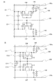
図1は、本実施の形態に示すマルチドメイン構造の液晶表示装置の一画素100の上面図
を示し、図2(A)は、図1に示す画素100の回路図を示し、図2(B)は従来の画素
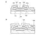
の回路図を示し、図3(A)は、図1に示す一点鎖線A−Bの断面図を示し、図3(B)
は、図1に示す一点鎖線C−Dの断面図を示す。図8(A)は、図1における薄膜トラン
ジスタ136及び薄膜トランジスタ137の近傍の拡大上面図である。図8(B)は、図
8(A)の走査線103、走査線103a、及び走査線103bの形状を見やすくするた
め、走査線103、走査線103a、走査線103b、容量配線105a、及び容量配線
105bのみハッチングを用いて示した上面図である。図8(C)は、図8(A)の第1
の電極123の形状を見やすくするため、信号線121、第1の電極123、第2の電極
125a、及び第3の電極125bのみハッチングを用いて示した上面図である。なお、
図8(B)及び図8(C)は、図1の一部を縮小して表示している。
1 is a top view of one
These show sectional drawing of the dashed-dotted line CD shown in FIG. FIG. 8A is an enlarged top view of the vicinity of the
In order to make the shape of the
8B and 8C show a part of FIG. 1 in a reduced size.
図1及び図2(A)に示すように、画素100には、走査線103と、走査線103と交
差する信号線121とを有する。また、走査線103と同じ方向に延びる容量配線105
a及び容量配線105bを有する。なお、容量配線105aと、容量配線105bとの間
に、走査線103を有する。
As shown in FIGS. 1 and 2A, the
a and a
また、走査線103及び信号線121の交差部近傍に薄膜トランジスタ136及び薄膜ト
ランジスタ137を有する。薄膜トランジスタ136は、走査線103に重畳する半導体
膜135と、半導体膜135と重畳する第1の電極123及び第2の電極125aを有す
る。第1の電極123は、信号線121から突出した領域である。第1の電極123及び
第2の電極125aは、薄膜トランジスタ136においてソース電極及びドレイン電極と
して機能する。
In addition, a
薄膜トランジスタ137は、走査線103に重畳する半導体膜135と、半導体膜135
と重畳する第1の電極123及び第3の電極125bとを有する。第1の電極123及び
第3の電極125bは、薄膜トランジスタ137においてソース電極及びドレイン電極と
して機能する。
The
And the
薄膜トランジスタ136に含まれる第2の電極125aは、画素電極139aと接続され
る。即ち、薄膜トランジスタ136は、第2の電極125aにより画素電極139aを含
む液晶素子142と接続する。また、容量素子140の一方の電極は画素電極139a及
び薄膜トランジスタ136の第2の電極125aと接続し、他方の電極は容量配線105
aと接続する(図2(A)参照。)。
The
a is connected (see FIG. 2A).
薄膜トランジスタ137に含まれる第3の電極125bは、画素電極139bと接続され
る。即ち、薄膜トランジスタ137は、第3の電極125bにより画素電極139bを含
む液晶素子143と接続する。また、容量素子141の一方の電極は画素電極139b及
び薄膜トランジスタ137の第3の電極125bと接続し、他方の電極は容量配線105
bと接続する(図2(A)参照。)。即ち、薄膜トランジスタ136及び薄膜トランジス
タ137は、上面形状において画素100の略中央に位置し、画素100における各サブ
画素の画素電極139a及び画素電極139bの間に形成される。薄膜トランジスタ13
6及び薄膜トランジスタ137を画素電極139a及び画素電極139bの間に設けるこ
とにより、第2の電極125a及び画素電極139a、並びに第3の電極125b及び画
素電極139bの接続距離を短くすることが可能であるため、第2の電極125a及び画
素電極139a、並びに第3の電極125b及び画素電極139bの間に発生する寄生容
量を低減すると共に、画素100における開口率の低減を防ぐことができる。
The
b is connected (see FIG. 2A). That is, the
6 and the
薄膜トランジスタ136及び薄膜トランジスタ137は、ソース電極及びドレイン電極の
一方である第1の電極123が共通している。即ち、各画素において、信号線から突出す
る電極が第1の電極123一つであり、且つ薄膜トランジスタ136及び薄膜トランジス
タ137において共通であるため、走査線103と信号線121から突出された第1の電
極123との間に発生する寄生容量を低減することができる。
The
また、走査線103は、薄膜トランジスタ136及び薄膜トランジスタ137が形成され
る領域近傍においてループ形状であり、走査線103a及び走査線103bとなっており
、開口部126を有する。即ち、走査線は、信号線121と交差する方向に延伸する領域
である走査線103と、間に開口部126を挟むことでループ形状を形成する走査線10
3a及び走査線103bとで構成される。このとき、開口部126を挟む走査線103a
及び走査線103bの幅の合計は、走査線103の幅以上である。また、ループ形状とな
っている走査線103a及び走査線103bにおいては、走査線103の端部より走査線
103a及び走査線103bの端部が外側に突出している(図8(B)参照。)。また、
ループ形状を形成する走査線103a及び走査線103bの間に設けられる開口部におい
て、第1の電極123の一部が配置される(図8(C)参照。)。走査線103a及び走
査線103bの幅の合計は、走査線103の幅以上であるため、走査線103から分岐し
た走査線103a及び走査線103bにおいて、配線抵抗の増加を防ぐことができると共
に、発熱、静電破壊等による半導体装置の不良の発生を低減することができる。
Further, the
3a and a
The total width of the
A part of the
なお、図2(A)及び図8(A)に示すように、薄膜トランジスタ136においては、走
査線103a及び第1の電極123の重畳部において寄生容量C4が発生する。また、走
査線103a及び第2の電極125aの重畳部において寄生容量C5が発生する。薄膜ト
ランジスタ137においては、走査線103b及び第1の電極123の重畳部において寄
生容量C6が発生する。また、走査線103b及び第3の電極125bの重畳部において
寄生容量C7が発生する。
Note that as shown in FIGS. 2A and 8A, in the
ここで、比較例として、薄膜トランジスタと重畳する領域においてループ形状を有せず、
直線状である走査線203を有し、薄膜トランジスタ236及び薄膜トランジスタ237
それぞれにおいて、信号線121と接続する電極が異なる画素200の回路図を図2(B
)に示す。図2(A)と同様の構成においては、同じ符号を用いて示し、構成の説明を省
略する。
Here, as a comparative example, there is no loop shape in the region overlapping with the thin film transistor,
The
2B is a circuit diagram of the
). 2A are denoted by the same reference numerals, and description of the structure is omitted.
図2(B)に示すように、画素200には、走査線203と、走査線203と交差する信
号線121とを有する。また、走査線203と同じ方向に延びる容量配線105a及び容
量配線105bを有する。なお、容量配線105aと、容量配線105bとの間に、走査
線203を有する。
As shown in FIG. 2B, the
また、走査線203及び信号線121の交差部近傍に薄膜トランジスタ236及び薄膜ト
ランジスタ237を有する。薄膜トランジスタ236は、走査線203に接続するゲート
電極と、信号線121から突出する第1の電極と、液晶素子142と接続する第2の電極
とを有する。また、容量素子140の一方の電極は、液晶素子142に含まれる画素電極
及び薄膜トランジスタ236の第2の電極に接続し、容量素子140の他方の電極は、容
量配線105aに接続する。
In addition, a
薄膜トランジスタ237は、走査線203に接続するゲート電極と、信号線121から突
出する第3の電極と、液晶素子143と接続する第4の電極とを有する。また、容量素子
141の一方の電極は、液晶素子143に含まれる画素電極及び薄膜トランジスタ237
の第4の電極に接続し、容量素子141の他方の電極は、容量配線105bに接続する。
The
The other electrode of the
なお、薄膜トランジスタ236においては、走査線203及び第1の電極の重畳部におい
て寄生容量C14が発生する。また、走査線203及び第2の電極の重畳部において寄生
容量C15が発生する。薄膜トランジスタ237においては、走査線203及び第3の電
極の重畳部において寄生容量C16が発生する。また、走査線203及び第4の電極の重
畳部において寄生容量C17が発生する。
Note that in the
薄膜トランジスタ136及び薄膜トランジスタ236のそれぞれにおいて、走査線103
a、203、及び第1の電極の重畳部の面積が略同一であれば、寄生容量C4及び寄生容
量C14は略同一である。また、走査線103a、203、及び第2の電極の重畳部の面
積が略同一であれば、寄生容量C5及び寄生容量C15は略同一である。薄膜トランジス
タ137及び薄膜トランジスタ237において、走査線103b及び第1の電極の重畳部
の面積と、走査線203及び第3の電極の重畳部の面積とが略同一であれば、寄生容量C
6及び寄生容量C16は略同一である。また、走査線103b及び第3の電極の重畳部の
面積と、走査線203及び第4の電極の重畳部の面積とが略同一であれば、寄生容量C7
及び寄生容量C17は略同一である。
In each of the
If the areas of the overlapping portions of a, 203 and the first electrode are substantially the same, the parasitic capacitance C4 and the parasitic capacitance C14 are substantially the same. Further, if the areas of the
6 and the parasitic capacitance C16 are substantially the same. In addition, if the area of the overlapping portion of the
The parasitic capacitance C17 is substantially the same.
比較例である、薄膜トランジスタと重畳する領域において、ループ形状を有せず、直線状
である走査線203を有する画素200は、図2(B)に示すように、走査線203及び
信号線121の間において、寄生容量C11が発生している。また、薄膜トランジスタ2
36及び薄膜トランジスタ237において、ソース電極及びドレイン電極の一方となる電
極が異なる電極(薄膜トランジスタ236においては第1の電極、薄膜トランジスタ23
7においては第3の電極)の場合、即ち、薄膜トランジスタ236の第1の電極及び薄膜
トランジスタ237の第3の電極のそれぞれと、信号線121とが接続する場合、走査線
203及び第1の電極の間に寄生容量C12が発生し、走査線203及び第3の電極の間
に寄生容量C13が発生する。
In the comparative example, in the region overlapping with the thin film transistor, the
36 and the
7 is the third electrode), that is, when each of the first electrode of the
しかしながら、本実施の形態に示す走査線103は、薄膜トランジスタ136及び薄膜ト
ランジスタ137が形成される領域近傍においてループ形状であり、図1及び図8(B)
に示すように、走査線103a及び走査線103bとなっており、開口部126を有する
。また、ループ形状である走査線103a及び走査線103bの間に設けられる開口部1
26において、第1の電極123が配置している(図8(C)参照。)。このため、当該
領域における第1の電極123において、走査線との寄生容量は生じていない。即ち、図
8(A)における寄生容量C3はゼロである。なお、走査線103a及び信号線121の
間、並びに走査線103b及び信号線121の間においては、それぞれ寄生容量C1及び
寄生容量C2が生じている。
However, the
As shown in FIG. 5, the
In FIG. 26, the
また、走査線103a及び走査線103bの幅の合計を走査線203の幅と、概略同一と
すると、画素200における寄生容量C11と、画素100における寄生容量C1及び寄
生容量C2の合計とは、略同一とすることが可能であるため、画素100と比較して、画
素200においては、寄生容量C12及び寄生容量C13が多い。
Further, if the total width of the
また、図1及び図2(A)に示す画素100において、薄膜トランジスタ136及び薄膜
トランジスタ137は、ソース電極及びドレイン電極の一方である第1の電極123が共
通している(図8(C)参照)。このため、第1の電極123において、抵抗が生じる。
1A and 1B, the
しかしながら、図2(B)に示すような、薄膜トランジスタ236及び薄膜トランジスタ
237において、ソース電極及びドレイン電極の一方となる電極が異なる電極の場合、即
ち、薄膜トランジスタ236の第1の電極及び薄膜トランジスタ237の第3の電極のそ
れぞれと、信号線121とが接続する場合、薄膜トランジスタ236の第1の電極及び薄
膜トランジスタ237の第3の電極のそれぞれにおいて、抵抗が生じる。
However, in the
これらのことから、図1及び図2(A)に示すように、信号線121から突出した第1の
電極123を、薄膜トランジスタ136及び薄膜トランジスタ137それぞれのソース電
極及びドレイン電極の一方とすることで、走査線103及び第1の電極123の重畳面積
を低減することが可能であり、配線幅を広げることなく、即ち、開口率を維持しつつ、走
査線103及び第1の電極123の間に生じる寄生容量を低減することができる。なお、
ここでは、走査線103a及び走査線103bの幅の合計を走査線203の幅と、概略同
一としたが、走査線103a及び走査線103bの幅の合計は、走査線103の幅以上で
あればよい。この結果、画素における走査線の抵抗の増加を防ぐことができる。
Accordingly, as illustrated in FIGS. 1 and 2A, the
Here, the total width of the
また、図1に示す画素100において、信号線121、第1の電極123、第2の電極1
25a、及び第3の電極125bと、走査線103a、走査線103b、容量配線105
a、及び容量配線105bとが交差する領域近傍において、信号線121、第1の電極1
23、第2の電極125a、及び第3の電極125bと、走査線103a、走査線103
b、容量配線105a、及び容量配線105bとの交差部の外側に、半導体膜135の端
部が位置する。即ち、走査線103a及び信号線121、走査線103b及び信号線12
1、容量配線105a及び信号線121、容量配線105b及び信号線121、走査線1
03a及び第1の電極123、走査線103a及び第2の電極125a、走査線103b
及び第3の電極125bの間において、ゲート絶縁膜のみでなく、半導体膜135が形成
されるため、配線間の寄生容量を低減できる。
Further, in the
25a, the
In the vicinity of the region where a and the
23, the
b, the end of the
1,
03a and the
Since not only the gate insulating film but also the
なお、本実施の形態に示す薄膜トランジスタは、第1の電極123を間として、第2の電
極125a及び第3の電極125bが設けられている。このため、第1の電極123から
第2の電極125aに流れる電流の方向と、第1の電極123から第3の電極125bに
流れる電流の方向が反対である。画素を2分割し、それぞれにチャネル方向(電流の流れ
る方向)の異なる薄膜トランジスタを設けることにより、半導体膜135の結晶性のばら
つきを原因とする、画素ごとの薄膜トランジスタの電気特性のばらつきを低減することが
できる。また、薄膜トランジスタ136及び薄膜トランジスタ137において、共通の半
導体膜を有するため、薄膜トランジスタ136及び薄膜トランジスタ137において、第
1の電極123及び半導体膜が接する領域を共有することができる。この結果、画素10
0における薄膜トランジスタ136及び薄膜トランジスタ137の専有面積を低減するこ
とが可能である。
Note that in the thin film transistor described in this embodiment, the
It is possible to reduce the area occupied by the
なお、本実施の形態においては、一画素に2つの薄膜トランジスタを設けた構造を示した
が、これに限定されない。一画素に3つ以上の複数の薄膜トランジスタ及び当該薄膜トラ
ンジスタに接続する複数の画素電極を有してもよい。
Note that although a structure in which two thin film transistors are provided for one pixel is described in this embodiment mode, the present invention is not limited to this. One pixel may include three or more thin film transistors and a plurality of pixel electrodes connected to the thin film transistors.
次に、薄膜トランジスタ及び容量素子の構造について、図3を用いて説明する。 Next, structures of the thin film transistor and the capacitor are described with reference to FIGS.
図3(A)は、図1に示す一点鎖線A−Bにおける薄膜トランジスタ136の断面構造で
ある。
FIG. 3A illustrates a cross-sectional structure of the
薄膜トランジスタ136は、基板101上に、走査線103と、半導体膜135と、走査
線103及び半導体膜135の間に設けられるゲート絶縁膜107と、半導体膜135に
接するソース領域及びドレイン領域として機能する不純物半導体膜127及び不純物半導
体膜129と、不純物半導体膜127に接する第1の電極123と、不純物半導体膜12
9に接する第2の電極125aとを有する。また、ゲート絶縁膜107、半導体膜135
、不純物半導体膜127、不純物半導体膜129、第1の電極123、及び第2の電極1
25aを覆う絶縁膜138が形成される。また、絶縁膜138の開口部において第2の電
極125aと接続する画素電極139aが形成される。
The
9 and a
,
An insulating
基板101としては、ガラス基板、セラミック基板の他、本作製工程の処理温度に耐えう
る程度の耐熱性を有するプラスチック基板等を用いることができる。また、基板に透光性
を要しない場合には、ステンレス等の金属の基板の表面に絶縁膜を設けたものを用いても
よい。ガラス基板としては、例えば、バリウムホウケイ酸ガラス、アルミノホウケイ酸ガ
ラス若しくはアルミノケイ酸ガラス等の無アルカリガラス基板を用いるとよい。なお、基
板101のサイズに限定はなく、例えば液晶表示装置でよく使われる第3世代乃至第10
世代のガラス基板を用いることができる。
As the
Generation glass substrates can be used.
走査線103の一部は薄膜トランジスタ136のゲート電極として機能する。走査線10
3は、モリブデン、チタン、クロム、タンタル、タングステン、アルミニウム、銅、ネオ
ジム、スカンジウム、ニッケル等の金属材料またはこれらを主成分とする合金材料を用い
て、単層でまたは積層して形成することができる。また、リン等の不純物元素をドーピン
グした多結晶シリコンに代表される半導体、Ag−Pd−Cu合金、Al−Nd合金、A
l−Ni合金などを用いてもよい。
A part of the
3 may be formed of a single layer or a stacked layer using a metal material such as molybdenum, titanium, chromium, tantalum, tungsten, aluminum, copper, neodymium, scandium, nickel, or an alloy material containing these as a main component. it can. Further, a semiconductor typified by polycrystalline silicon doped with an impurity element such as phosphorus, an Ag—Pd—Cu alloy, an Al—Nd alloy, A
An l-Ni alloy or the like may be used.
例えば、走査線103の二層の積層構造としては、アルミニウム膜上にモリブデン膜を積
層した二層の積層構造、または銅膜上にモリブデン膜を積層した二層構造、または銅膜上
に窒化チタン膜若しくは窒化タンタル膜を積層した二層構造、窒化チタン膜とモリブデン
膜とを積層した二層構造、酸素を含む銅−マグネシウム合金膜と銅膜とを積層した二層構
造、酸素を含む銅−マンガン合金膜と銅膜とを積層した二層構造、銅−マンガン合金膜と
銅膜とを積層した二層構造などとすることが好ましい。三層の積層構造としては、タング
ステン膜または窒化タングステン膜と、アルミニウムとシリコンの合金膜またはアルミニ
ウムとチタンの合金膜と、窒化チタン膜またはチタン膜とを積層した三層構造とすること
が好ましい。電気的抵抗が低い膜上にバリア膜として機能する金属膜が積層されることで
、電気的抵抗を低くでき、且つ金属膜から半導体膜への金属元素の拡散を防止することが
できる。
For example, the two-layer structure of the
なお、走査線103と同時に、容量配線105a及び容量配線105bが形成される。こ
のため、容量配線105a及び容量配線105bは、走査線103と同様の材料及び積層
構造を有する。
Note that the
ゲート絶縁膜107は、酸化シリコン膜、酸化窒化シリコン膜、窒化シリコン膜、窒化酸
化シリコン膜、酸化アルミニウム膜、窒化アルミニウム膜、酸化窒化アルミニウム膜、ま
たは窒化酸化アルミニウム膜を、単層でまたは積層して形成することができる。なお、ゲ
ート絶縁膜107において、半導体膜135が微結晶シリコン膜の場合、半導体膜135
と接する層を、酸化シリコン膜、酸化アルミニウム膜等の酸化物膜で形成することで、半
導体膜135との界面の窒素濃度を低減できるため、薄膜トランジスタの電気特性の信頼
性を高めることができる。
The
When the layer in contact with the
なお、ここでは、酸化窒化シリコンとは、その組成として、窒素よりも酸素の含有量が多
いものであって、好ましくは、ラザフォード後方散乱法(RBS:Rutherford
Backscattering Spectrometry)及び水素前方散乱法(H
FS:Hydrogen Forward Scattering Spectrome
try)を用いて測定した場合に、組成範囲として酸素が50〜70原子%、窒素が0.
5〜15原子%、シリコンが25〜35原子%、水素が0.1〜10原子%の範囲で含ま
れるものをいう。また、窒化酸化シリコンとは、その組成として、酸素よりも窒素の含有
量が多いものであって、好ましくは、RBS及びHFSを用いて測定した場合に、組成範
囲として酸素が5〜30原子%、窒素が20〜55原子%、シリコンが25〜35原子%
、水素が10〜30原子%の範囲で含まれるものをいう。ただし、酸化窒化シリコンまた
は窒化酸化シリコンを構成する原子の合計を100原子%としたとき、窒素、酸素、シリ
コン及び水素の含有比率が上記の範囲内に含まれるものとする。
Note that, here, silicon oxynitride has a composition containing more oxygen than nitrogen, and preferably, Rutherford backscattering method (RBS: Rutherford).
Backscattering Spectrometry) and hydrogen forward scattering (H
FS: Hydrogen Forward Scattering Spectrome
(try), the composition range of oxygen is 50 to 70 atomic%, nitrogen is 0.
5-15 atomic%, silicon is 25-35 atomic%, and hydrogen is included in the range of 0.1-10 atomic%. In addition, silicon nitride oxide has a composition containing more nitrogen than oxygen, and preferably has a composition range of 5 to 30 atomic% when measured using RBS and HFS. , Nitrogen is 20-55 atomic%, silicon is 25-35 atomic%
, Which contains hydrogen in the range of 10 to 30 atomic%. However, when the total number of atoms constituting silicon oxynitride or silicon nitride oxide is 100 atomic%, the content ratio of nitrogen, oxygen, silicon, and hydrogen is included in the above range.
半導体膜135は、シリコンまたはシリコンゲルマニウムを用いて形成する。または、酸
化物半導体を用いて形成する。酸化物半導体の代表例としては、四元系金属酸化物である
In−Sn−Ga−Zn−O膜や、三元系金属酸化物であるIn−Ga−Zn−O膜、I
n−Sn−Zn−O膜、In−Al−Zn−O膜、Sn−Ga−Zn−O膜、Al−Ga
−Zn−O膜、Sn−Al−Zn−O膜や、二元系金属酸化物であるIn−Zn−O膜、
Sn−Zn−O膜、Al−Zn−O膜、In−Ga−O膜などを用いることができる。
The
n-Sn-Zn-O film, In-Al-Zn-O film, Sn-Ga-Zn-O film, Al-Ga
-Zn-O film, Sn-Al-Zn-O film, In-Zn-O film which is a binary metal oxide,
An Sn—Zn—O film, an Al—Zn—O film, an In—Ga—O film, or the like can be used.
また、半導体膜135は、上記半導体材料のいずれかを用いた、非晶質半導体、微結晶半
導体、または結晶性半導体を、単層または積層して形成することができる。
The
なお、微結晶半導体とは、非晶質と結晶構造(単結晶、多結晶を含む)の中間的な構造の
半導体である。微結晶半導体は、自由エネルギー的に安定な第3の状態を有する半導体で
あって、短距離秩序を持ち格子歪みを有する結晶質な半導体であり、混相粒径が2nm以
上200nm以下、好ましくは10nm以上80nm以下、より好ましくは、20nm以
上50nm以下の柱状または針状の混相粒が基板表面に対して法線方向に成長している。
このため、柱状または針状の混相粒の界面には、粒界が形成される場合もある。
Note that a microcrystalline semiconductor is a semiconductor having an intermediate structure between amorphous and crystalline structures (including single crystal and polycrystal). A microcrystalline semiconductor is a semiconductor having a third state which is stable in terms of free energy, and is a crystalline semiconductor having a short-range order and lattice distortion, and a mixed phase particle size of 2 nm to 200 nm, preferably 10 nm. Columnar or needle-like mixed phase grains having a size of 80 nm or more and more preferably 20 nm or more and 50 nm or less grow in a normal direction with respect to the substrate surface.
For this reason, a grain boundary may be formed at the interface between the columnar or needle-like mixed phase grains.
微結晶半導体の代表例である微結晶シリコンは、そのラマンスペクトルが単結晶シリコン
を示す520cm−1より低波数側に、シフトしている。即ち、単結晶シリコンを示す5
20cm−1とアモルファスシリコンを示す480cm−1の間に微結晶シリコンのラマ
ンスペクトルのピークがある。また、未結合手(ダングリングボンド)を終端するため水
素またはハロゲンを少なくとも1原子%含んでいる。さらに、ヘリウム、アルゴン、ネオ
ン、クリプトン、キセノンなどの希ガス元素を含ませて格子歪みをさらに助長させること
で、安定性が増し良好な微結晶半導体が得られる。このような微結晶半導体に関する記述
は、例えば、米国特許4,409,134号で開示されている。
Microcrystalline silicon which is a typical example of a microcrystalline semiconductor has its Raman spectrum shifted to a lower wave number side than 520 cm −1 indicating single crystal silicon. That is, 5 indicating single crystal silicon.
There is a Raman spectrum peak of microcrystalline silicon between 20 cm −1 and 480 cm −1 indicating amorphous silicon. Further, in order to terminate dangling bonds (dangling bonds), it contains at least 1 atomic% of hydrogen or halogen. Further, by adding a rare gas element such as helium, argon, neon, krypton, or xenon to further promote lattice distortion, a stable microcrystalline semiconductor with improved stability can be obtained. A description of such a microcrystalline semiconductor is disclosed in, for example, US Pat. No. 4,409,134.
ここでは、半導体膜135として、微結晶半導体領域131及び非晶質半導体領域133
の積層構造を適用する。
Here, the
The laminated structure is applied.
微結晶半導体領域131は表面が鋭角な凹凸状であり、凸部はゲート絶縁膜107から非
晶質半導体領域133に向かって、先端が狭まる(凸部の先端が鋭角である)凸状(錐形
状)である。なお、微結晶半導体領域131の凹凸の形状は、ゲート絶縁膜107から非
晶質半導体領域133に向かって幅が広がる凸状(逆錐形状)であってもよい。
The
微結晶半導体領域131において、少なくとも凸部の領域は、窒素濃度の高い領域である
。また、微結晶半導体領域131に含まれる結晶粒界に、NH基またはNH2基を有して
もよい。二次イオン質量分析法によって計測される微結晶半導体領域131の凸部の領域
に含まれる窒素の濃度を、1×10²⁰atoms/cm3以上1×1021atoms
/cm3以下、好ましくは2×1020atoms/cm3以上1×1021atoms
/cm3以下とすることで、錐形状または逆錐形状を含む凹凸を形成することが可能であ
る。
In the
/ Cm 3 or less, preferably 2 × 10 20 atoms / cm 3 or more and 1 × 10 21 atoms
By setting it to / cm 3 or less, it is possible to form irregularities including a cone shape or an inverted cone shape.
非晶質半導体領域133は、窒素を有する非晶質半導体で形成される。窒素を有する非晶
質半導体に含まれる窒素は、例えばNH基またはNH2基として存在していてもよい。非
晶質半導体としては、アモルファスシリコンを用いて形成する。
The
窒素を含む非晶質半導体は、従来の非晶質半導体と比較して、CPM(Constant
photocurrent method)やフォトルミネッセンス分光測定で測定さ
れるUrbach端のエネルギーが小さく、欠陥吸収スペクトル量が少ない半導体である
。即ち、窒素を含む非晶質半導体は、従来の非晶質半導体と比較して、欠陥が少なく、価
電子帯のバンド端における準位のテール(裾)の傾きが急峻である秩序性の高い半導体で
ある。窒素を含む非晶質半導体は、価電子帯のバンド端における準位のテール(裾)の傾
きが急峻であるため、バンドギャップが広くなり、トンネル電流が流れにくい。このため
、窒素を含む非晶質半導体を、微結晶半導体領域131と不純物半導体膜127及び不純
物半導体膜129との間に設けることで、薄膜トランジスタのオフ電流を低減することが
できる。また、窒素を含む非晶質半導体を設けることで、オン電流と電界効果移動度を高
めることが可能である。
An amorphous semiconductor containing nitrogen is more CPM (Constant) than a conventional amorphous semiconductor.
The semiconductor has a small energy at the Urbach end measured by photocurrent method and photoluminescence spectroscopy, and has a small amount of defect absorption spectrum. That is, an amorphous semiconductor containing nitrogen has a high degree of ordering with fewer defects and a steep slope of the level tail at the band edge of the valence band than a conventional amorphous semiconductor. It is a semiconductor. An amorphous semiconductor containing nitrogen has a steep inclination of a level tail at the band edge of the valence band, so that a band gap becomes wide and a tunnel current hardly flows. Therefore, by providing an amorphous semiconductor containing nitrogen between the
さらに、窒素を含む非晶質半導体は、低温フォトルミネッセンス分光によるスペクトルの
ピーク領域が、1.31eV以上1.39eV以下である。なお、微結晶半導体、代表的
には微結晶シリコンを低温フォトルミネッセンス分光により測定したスペクトルのピーク
領域は、0.98eV以上1.02eV以下であり、窒素を含む非晶質半導体は、微結晶
半導体とは異なるものである。
Further, an amorphous semiconductor containing nitrogen has a peak region of a spectrum by low temperature photoluminescence spectroscopy of 1.31 eV or more and 1.39 eV or less. Note that a peak region of a spectrum of microcrystalline semiconductor, typically microcrystalline silicon measured by low-temperature photoluminescence spectroscopy, is 0.98 eV or more and 1.02 eV or less, and an amorphous semiconductor containing nitrogen is a microcrystalline semiconductor. Is different.
また、非晶質半導体領域133に、粒径が1nm以上10nm以下、好ましくは1nm以
上5nm以下の半導体結晶粒を含ませることで、更に薄膜トランジスタのオン電流と電界
効果移動度を高めることが可能である。
In addition, when the
不純物半導体膜127及び不純物半導体膜129は、必要に応じて設ければよい。例えば
、半導体膜をシリコン膜またはシリコンゲルマニウム膜で形成する場合であって、且つn
チャネル型薄膜トランジスタの場合は、リンが添加されたアモルファスシリコン、リンが
添加された微結晶シリコン等を用いて形成する。また、リンが添加されたアモルファスシ
リコン及びリンが添加された微結晶シリコンの積層構造とすることもできる。なお、pチ
ャネル型薄膜トランジスタの場合は、不純物半導体膜127及び不純物半導体膜129は
、ホウ素が添加された微結晶シリコン、ホウ素が添加されたアモルファスシリコン等を用
いて形成する。
The
In the case of a channel thin film transistor, amorphous silicon to which phosphorus is added, microcrystalline silicon to which phosphorus is added, or the like is used. Alternatively, a stacked structure of amorphous silicon to which phosphorus is added and microcrystalline silicon to which phosphorus is added can be used. Note that in the case of a p-channel thin film transistor, the
第1の電極123及び第2の電極125aは、アルミニウム、銅、チタン、ネオジム、ス
カンジウム、モリブデン、クロム、タンタル若しくはタングステン等により単層で、また
は積層して形成することができる。または、ヒロック防止元素が添加されたアルミニウム
合金(走査線103に用いることができるAl−Nd合金等)により形成してもよい。ド
ナーとなる不純物元素を添加した結晶性シリコンを用いてもよい。ドナーとなる不純物元
素が添加された結晶性シリコンと接する側の膜を、チタン、タンタル、モリブデン、タン
グステンまたはこれらの元素の窒化物により形成し、その上にアルミニウムまたはアルミ
ニウム合金を形成した積層構造としてもよい。更には、アルミニウムまたはアルミニウム
合金の上面及び下面を、チタン、タンタル、モリブデン、タングステンまたはこれらの元
素の窒化物で挟んだ積層構造としてもよい。
The
なお、第1の電極123及び第2の電極125aと同時に、第3の電極125bが形成さ
れる。このため、第3の電極125bは、第1の電極123及び第2の電極125aと同
様の材料及び積層構造を有する。また、第1の電極123は、信号線121の一部が突出
した領域である。このため、信号線121は、第1の電極123と同様の材料及び積層構
造を有する。
Note that the
絶縁膜138は、ゲート絶縁膜107と同様の材料を適宜用いることができる。なお、絶
縁膜138を積層構造とする場合は、半導体膜135に接する層を、酸化シリコン膜、酸
化アルミニウム膜等の酸化物膜で形成することが好ましい。これは、絶縁膜138上にバ
ックゲート電極を設ける場合、半導体膜135において絶縁膜138に接する領域はチャ
ネル領域として機能する。チャネル領域における窒素濃度を低減させることで、薄膜トラ
ンジスタの信頼性を高めることができるためである。
The insulating
画素電極139aは、酸化タングステンを含むインジウム酸化物、酸化タングステンを含
むインジウム亜鉛酸化物、酸化チタンを含むインジウム酸化物、酸化チタンを含むインジ
ウム錫酸化物、インジウム錫酸化物、インジウム亜鉛酸化物、または酸化シリコンを添加
したインジウム錫酸化物等の透光性を有する導電性材料や、グラフェンを用いて形成する
ことができる。
The
画素電極139aと同時に、画素電極139bが形成される。このため、画素電極139
bは、画素電極139aと同様の材料及び積層構造を有する。
A
b has the same material and laminated structure as the
図3(B)は、図1に示す一点鎖線C−Dにおける容量素子の断面構造である。 FIG. 3B illustrates a cross-sectional structure of the capacitor along dashed-dotted line CD in FIG.
容量素子140は、基板101上に、容量配線105aと、第2の電極125aと、容量
配線105a及び第2の電極125aの間に設けられるゲート絶縁膜107とで構成され
る。また、ゲート絶縁膜107及び第2の電極125aを覆う絶縁膜138が形成される
。また、絶縁膜138上に第2の電極125aと接続する画素電極139aが形成される
。
The
なお、図示しないが、薄膜トランジスタ137は、薄膜トランジスタ136と同様の構造
で構成される。また、薄膜トランジスタ137に接続する容量素子141は、容量素子1
40と同様の構造で構成される。
Note that although not illustrated, the
40 and the same structure.
本実施の形態により、マルチドメイン構造の液晶表示装置において、走査線及び信号線の
間、薄膜トランジスタの走査線と、ソース電極及びドレイン電極の一方との寄生容量を低
減することができる。このため、大型である液晶表示装置、高速駆動が可能な液晶表示装
置、解像度の高い液晶表示装置において、表示品質を向上させることができる。また、液
晶表示装置の消費電力を低減することができる。
According to this embodiment mode, in the multi-domain liquid crystal display device, parasitic capacitance between the scan line and the signal line, and between the scan line of the thin film transistor and one of the source electrode and the drain electrode can be reduced. Therefore, display quality can be improved in a large-sized liquid crystal display device, a liquid crystal display device that can be driven at high speed, and a liquid crystal display device with high resolution. In addition, power consumption of the liquid crystal display device can be reduced.
なお、本実施の形態に示す構成は、他の実施の形態に示す構成と適宜組み合わせて用い
ることができる。
Note that the structure described in this embodiment can be combined as appropriate with any of the structures described in the other embodiments.
(実施の形態2)
本実施の形態では、配線容量を低減した液晶表示装置において、実施の形態1と異なる構
造を有する一画素の構成について、図4及び図5を用いて説明する。なお、本実施の形態
では、1画素に複数のサブ画素を設けた画素を、画素150として説明するがこれに限定
されるものではない。
(Embodiment 2)
In this embodiment, a structure of one pixel having a structure different from that in
図4は、本実施の形態に示すマルチドメイン構造の液晶表示装置の一画素150の上面図
であり、図5は、図4に示す一点鎖線E−Fの断面図を示す。
4 is a top view of one
図4に示すように、画素150には、走査線103と、走査線103と交差する信号線1
51とを有する。また、走査線103と同じ方向に延びる容量配線105a及び容量配線
105bを有する。なお、容量配線105aと、容量配線105bとの間に、走査線10
3を有する。
As shown in FIG. 4, the
51. In addition, a
3.
また、走査線103及び信号線151の交差部近傍に薄膜トランジスタ166及び薄膜ト
ランジスタ167を有する。薄膜トランジスタ166は、走査線103に重畳する半導体
膜165aと、半導体膜165aと重畳する第1の電極153及び第2の電極155aと
を有する。第1の電極153は、信号線151から突出した領域である。第1の電極15
3及び第2の電極155aは、薄膜トランジスタ166においてソース電極及びドレイン
電極として機能する。
In addition, a
The third and
薄膜トランジスタ167は、走査線103に重畳する半導体膜165bと、半導体膜16
5bと重畳する第1の電極153及び第3の電極155bとを有する。第1の電極153
及び第3の電極155bは、薄膜トランジスタ167においてソース電極及びドレイン電
極として機能する。
The thin film transistor 167 includes a
A
The
薄膜トランジスタ166に含まれる第2の電極155aは、画素電極169aと接続され
る。また、容量配線105aと、第2の電極155a及び画素電極169aのそれぞれ一
部とが重畳している。容量配線105a、ゲート絶縁膜、及び第2の電極155aにより
容量素子を構成する。
The
薄膜トランジスタ167に含まれる第3の電極155bは、画素電極169bと接続され
る。また、容量配線105bと、第3の電極155b及び画素電極169bのそれぞれ一
部とが重畳している。容量配線105b、ゲート絶縁膜、及び第3の電極155bにより
容量素子を構成する。即ち、薄膜トランジスタ166及び薄膜トランジスタ167は、薄
膜トランジスタ136及び薄膜トランジスタ137と同様に、上面形状において画素15
0の略中央に位置し、画素150における各サブ画素の画素電極169a及び画素電極1
69bの間に形成される。このため、第2の電極155a及び画素電極169a、並びに
第3の電極155b及び画素電極169bの間に発生する寄生容量を低減すると共に、画
素150における開口率の低減を防ぐことができる。
The
0, the
69b. Therefore, parasitic capacitance generated between the
薄膜トランジスタ166及び薄膜トランジスタ167は、ソース電極及びドレイン電極の
一方である第1の電極153が共通している。即ち、各画素において、信号線から突出す
る電極が第1の電極153一つであり、且つ薄膜トランジスタ166及び薄膜トランジス
タ167において共通であるため、走査線103と信号線151から突出された第1の電
極153との間に発生する寄生容量を低減することができる。
The
また、走査線103は、薄膜トランジスタ166及び薄膜トランジスタ167が形成され
る領域近傍においてループ形状であり、走査線103a及び走査線103bとなっている
。また、ループ形状である走査線103a及び走査線103bとの間に設けられる開口部
において、第1の電極153の一部が配置される。このため、薄膜トランジスタ166及
び薄膜トランジスタ167それぞれに、ソース電極及びドレイン電極の一方が設けられる
場合と比較して、走査線103及び第1の電極153の重畳面積を低減することが可能で
あり、走査線103及び第1の電極153の間に生じる寄生容量を低減することができる
。また、走査線103a及び走査線103bの幅の合計は、走査線103の幅以上である
ため、走査線103から分岐した走査線103a及び走査線103bにおいて、配線抵抗
の増加を防ぐことができると共に、発熱、静電破壊等による半導体装置の不良の発生を低
減することができる。
Further, the
これらのことから、走査線103及び第1の電極153の重畳面積を低減することが可能
であり、配線幅を広げることなく、即ち、開口率を維持しつつ、走査線103及び第1の
電極153の間に生じる寄生容量を低減することができる。また、画素における抵抗を低
減することができる。
Accordingly, the overlapping area of the
また、図4に示す画素150において、走査線103a及び信号線151、走査線103
b及び信号線151、容量配線105a及び信号線151、並びに容量配線105b及び
信号線151の間において、半導体膜165cが設けられている。また、走査線103a
及び信号線151、走査線103b及び信号線151、容量配線105a及び信号線15
1、並びに容量配線105b及び信号線151それぞれの交差部より外側に、半導体膜1
65cの端部が位置する。このため、上記配線間には、ゲート絶縁膜のみでなく、半導体
膜165cが形成されるため、配線間の寄生容量を低減できる。なお、半導体膜165c
の端部は、走査線103の一端部と重畳しているため、走査線103の一端部及び第1の
電極153の一部における寄生容量を低減している。
In the
A semiconductor film 165 c is provided between the
And the
1, and the
The end of 65c is located. Therefore, not only the gate insulating film but also the semiconductor film 165c is formed between the wirings, so that parasitic capacitance between the wirings can be reduced. Note that the semiconductor film 165c
Since this end portion overlaps with one end portion of the
また、薄膜トランジスタ166及び薄膜トランジスタ167のそれぞれにおいて、半導体
膜165a及び半導体膜165bの端部は、走査線103の内側に位置する。このため、
半導体膜165a及び半導体膜165bへのバックライトや外光の照射を低減することが
可能であり、薄膜トランジスタ166及び薄膜トランジスタ167の光リーク電流を低下
することができる。
In each of the
Irradiation of the backlight and the external light to the
なお、本実施の形態に示す薄膜トランジスタは、上面形状において、第1の電極153の
一方の辺側に、第2の電極155a及び第3の電極155bが設けられている。即ち、第
2の電極155a及び第3の電極155bと、信号線151との間に、信号線から突出す
る第1の電極153が設けられる。このため、第1の電極153及び第2の電極155a
の間に流れる電流の方向と、第1の電極153及び第3の電極155bの間に流れる電流
の方向とが略一致する。半導体膜が微結晶半導体膜または結晶性半導体膜の場合、結晶の
配向方向と、上記電流の流れる方向を略一致させることで、薄膜トランジスタの電気特性
を向上させることができる。また、薄膜トランジスタ166及び薄膜トランジスタ167
が有する半導体膜がそれぞれ異なるため、薄膜トランジスタ同士におけるリーク電流が少
なく、更には、一方の薄膜トランジスタの電気特性が悪くとも、一方の薄膜トランジスタ
の電気特性が他方の薄膜トランジスタの電気特性に影響しないため、画素間の電気特性の
ムラを低減することができる。
Note that in the top surface shape of the thin film transistor described in this embodiment, the
The direction of the current flowing between the
Since each semiconductor film has different characteristics, there is little leakage current between thin film transistors, and even if the electrical characteristics of one thin film transistor are poor, the electrical characteristics of one thin film transistor do not affect the electrical characteristics of the other thin film transistor. The unevenness of the electrical characteristics can be reduced.
なお、本実施の形態においては、一画素に2つの薄膜トランジスタを設けた構造を示した
が、これに限定されない。一画素に3つ以上の複数の薄膜トランジスタ及び当該薄膜トラ
ンジスタに接続する複数の画素電極を有してもよい。
Note that although a structure in which two thin film transistors are provided for one pixel is described in this embodiment mode, the present invention is not limited to this. One pixel may include three or more thin film transistors and a plurality of pixel electrodes connected to the thin film transistors.
次に、薄膜トランジスタの構造について、図5を用いて説明する。 Next, the structure of the thin film transistor is described with reference to FIGS.
図5は、図4に示す一点鎖線E−Fにおける薄膜トランジスタ166の断面構造である。
FIG. 5 illustrates a cross-sectional structure of the
薄膜トランジスタ166は、基板101上に、走査線103と、半導体膜165aと、走
査線103及び半導体膜165aの間に設けられるゲート絶縁膜107と、半導体膜16
5aに接するソース領域及びドレイン領域として機能する不純物半導体膜157及び不純
物半導体膜159と、不純物半導体膜157に接する第1の電極153と、不純物半導体
膜159に接する第2の電極155aとを有する。また、ゲート絶縁膜107、半導体膜
165a、不純物半導体膜157、不純物半導体膜159、第1の電極153、及び第2
の電極155aを覆う絶縁膜168が形成される。また、絶縁膜168の開口部において
第2の電極155aと接続する画素電極169aが形成される。
The
The
An insulating
半導体膜165aは、実施の形態1に示す半導体膜135と同様の材料及び構造を適宜用
いることができる。
For the
なお、半導体膜165aと同時に、半導体膜165bが形成される。このため、半導体膜
165bは、半導体膜165aと同様の材料及び積層構造を有する。
Note that the
不純物半導体膜157及び不純物半導体膜159は、必要に応じて設ければよい。また、
不純物半導体膜157及び不純物半導体膜159を設ける場合は、実施の形態1に示す不
純物半導体膜127及び不純物半導体膜129と同様の材料及び構造を適宜用いることが
できる。
The
In the case where the
第1の電極153及び第2の電極155aは、実施の形態1に示す第1の電極123及び
第2の電極125aと同様の材料及び構造を適宜用いることができる。
For the
なお、第1の電極153及び第2の電極155aと同時に、第3の電極155bが形成さ
れる。このため、第3の電極155bは、第1の電極153及び第2の電極155aと同
様の材料及び積層構造を有する。また、第1の電極153は、信号線151の一部が突出
した領域である。このため、信号線151は、第1の電極153と同様の材料及び積層構
造を有する。
Note that the
絶縁膜168は、実施の形態1に示す絶縁膜138と同様の材料及び構造を適宜用いるこ
とができる。
For the insulating
画素電極169aは、実施の形態1に示す画素電極139aと同様の材料及び構造を適宜
用いることができる。
For the
なお、画素電極169aと同時に、画素電極169bが形成される。このため、画素電極
169bは、画素電極169aと同様の材料及び積層構造を有する。
Note that the
本実施の形態により、マルチドメイン構造の液晶表示装置において、走査線及び信号線の
間、薄膜トランジスタの走査線と、ソース電極及びドレイン電極の一方との寄生容量を低
減することができる。このため、大型である液晶表示装置、高速駆動が可能な液晶表示装
置、解像度の高い液晶表示装置において、表示品質を向上させることができる。また、液
晶表示装置の消費電力を低減することができる。
According to this embodiment mode, in the multi-domain liquid crystal display device, parasitic capacitance between the scan line and the signal line, and between the scan line of the thin film transistor and one of the source electrode and the drain electrode can be reduced. Therefore, display quality can be improved in a large-sized liquid crystal display device, a liquid crystal display device that can be driven at high speed, and a liquid crystal display device with high resolution. In addition, power consumption of the liquid crystal display device can be reduced.
なお、本実施の形態に示す構成は、他の実施の形態に示す構成と適宜組み合わせて用い
ることができる。
Note that the structure described in this embodiment can be combined as appropriate with any of the structures described in the other embodiments.
(実施の形態3)
本実施の形態では、実施の形態1及び実施の形態2に示す薄膜トランジスタの作製方法に
ついて、図6及び図7を用いて説明する。なお、ここでは、実施の形態1に示す薄膜トラ
ンジスタ136の作製方法を説明するが、適宜実施の形態1に示す薄膜トランジスタ13
7、実施の形態2に示す薄膜トランジスタ166及び薄膜トランジスタ167に適用する
ことができる。なお、薄膜トランジスタは、p型よりもn型の方が、キャリアの移動度が
高い。また、同一の基板上に形成する薄膜トランジスタを全て同じ極性に統一すると、工
程数を抑えることができ、好ましい。そのため、本実施の形態では、n型の薄膜トランジ
スタの作製方法について説明する。
(Embodiment 3)
In this embodiment, a method for manufacturing the thin film transistor described in any of
7. This embodiment can be applied to the
図6(A)に示すように、基板101上に走査線103を形成する。次に、走査線103
を覆うゲート絶縁膜107を形成し、ゲート絶縁膜107上に微結晶半導体膜109を形
成する。
As shown in FIG. 6A, the
A
走査線103は、基板101上に、スパッタリング法または真空蒸着法を用いて、上記し
た材料により導電膜を形成し、該導電膜上にフォトリソグラフィ法またはインクジェット
法等によりマスクを形成し、該マスクを用いて導電膜をエッチングして形成することがで
きる。また、銀、金または銅等の導電性ナノペーストをインクジェット法により基板上に
吐出し、焼成することで形成することもできる。なお、走査線103及び基板101の密
着性向上を目的として、上記の金属材料の窒化物膜を、基板101と、走査線103との
間に設けてもよい。ここでは、基板101上に導電膜を形成し、フォトリソグラフィ工程
により形成したレジストで形成されるマスクを用いて、当該導電膜をエッチングする。
The
なお、走査線103の側面は、テーパー形状とすることが好ましい。これは、後の工程で
、走査線103上に形成される絶縁膜、半導体膜及び配線が、走査線103の段差箇所に
おいて切断されないようにするためである。走査線103の側面をテーパー形状にするた
めには、レジストで形成されるマスクを後退させつつエッチングを行えばよい。
Note that the side surface of the
また、走査線103を形成する工程により、容量配線105a及び容量配線105bを同
時に形成することができる。
Further, the
ゲート絶縁膜107は、CVD法またはスパッタリング法等を用いて形成することができ
る。ゲート絶縁膜107を形成する際のグロー放電プラズマの生成は、3MHzから30
MHz、代表的には13.56MHz、27.12MHzのHF帯の高周波電力、または
30MHzより大きく300MHz程度までのVHF帯の高周波電力、代表的には、60
MHzを印加することで行われる。また、1GHz以上のマイクロ波の高周波電力を印加
することで行われる。なお、高周波電力がパルス状に印加されるパルス発振や、連続的に
印加される連続発振とすることができる。また、HF帯の高周波電力と、VHF帯の高周
波電力とを重畳させることで、大面積基板においてもプラズマのムラを低減し、均一性を
高めることができると共に、堆積速度を高めることができる。高周波数が1GHz以上で
あるマイクロ波プラズマCVD装置を用いてゲート絶縁膜107を形成すると、ゲート電
極と、ドレイン電極及びソース電極との間の耐圧を向上させることができるため、信頼性
の高い薄膜トランジスタを得ることができる。
The
MHz, typically 13.56 MHz, 27.12 MHz high frequency power in the HF band, or high frequency power in the VHF band greater than 30 MHz up to about 300 MHz, typically 60
This is done by applying MHz. Further, it is performed by applying microwave high frequency power of 1 GHz or more. Note that pulse oscillation in which high-frequency power is applied in a pulsed manner or continuous oscillation in which high-frequency power is continuously applied can be employed. In addition, by superimposing high frequency power in the HF band and high frequency power in the VHF band, plasma unevenness can be reduced even in a large-area substrate, uniformity can be increased, and the deposition rate can be increased. When the
また、ゲート絶縁膜107として、有機シランガスを用いたCVD法により酸化シリコン
膜を形成することで、後に形成する半導体膜の結晶性を高めることが可能であるため、薄
膜トランジスタのオン電流及び電界効果移動度を高めることができる。有機シランガスと
しては、テトラメチルシラン(TMS:化学式Si(CH3)4)、テトラメチルシクロ
テトラシロキサン(TMCTS)、オクタメチルシクロテトラシロキサン(OMCTS)
、ヘキサメチルジシラザン(HMDS)、トリエトキシシラン(SiH(OC2H5)3
)、トリスジメチルアミノシラン(SiH(N(CH3)2)3)等のシリコン含有化合
物を用いることができる。
In addition, by forming a silicon oxide film as the
, Hexamethyldisilazane (HMDS), triethoxysilane (SiH (OC 2 H 5 ) 3
), Trisdimethylaminosilane (SiH (N (CH 3 ) 2 ) 3 ), and other silicon-containing compounds can be used.
微結晶半導体膜109は、プラズマCVD装置の反応室内において、シリコンまたはゲル
マニウムを含む堆積性気体と、水素とを混合し、グロー放電プラズマにより形成する。ま
たは、シリコンまたはゲルマニウムを含む堆積性気体と、水素と、ヘリウム、アルゴン、
ネオン、クリプトン、キセノン等の希ガスとを混合し、グロー放電プラズマにより形成す
る。ここでは、シリコンまたはゲルマニウムを含む堆積性気体の流量に対する水素の流量
を50倍以上1000倍以下にして堆積性気体を希釈する条件により、微結晶シリコン、
微結晶シリコンゲルマニウム等を形成する。このときの堆積温度は、室温〜350℃とす
ることが好ましく、より好ましくは150〜280℃とする。なお、上部電極及び下部電
極の間隔は、プラズマが発生しうる間隔とすればよい。
The
A rare gas such as neon, krypton, or xenon is mixed and formed by glow discharge plasma. Here, the microcrystalline silicon is diluted by a condition in which the flow rate of hydrogen with respect to the flow rate of the deposition gas containing silicon or germanium is 50 to 1000 times to dilute the deposition gas,
Microcrystalline silicon germanium or the like is formed. The deposition temperature at this time is preferably room temperature to 350 ° C., more preferably 150 to 280 ° C. Note that the interval between the upper electrode and the lower electrode may be an interval at which plasma can be generated.
シリコンまたはゲルマニウムを含む堆積性気体の代表例としては、SiH4、Si2H6
、GeH4、Ge2H6等がある。
Typical examples of the deposition gas containing silicon or germanium include SiH 4 and Si 2 H 6.
, GeH 4 , Ge 2 H 6 and the like.
なお、微結晶半導体膜109の原料ガスに、ヘリウム、アルゴン、ネオン、クリプトン、
キセノン等の希ガスを添加することで、微結晶半導体膜109の成膜速度が高まる。この
結果、成膜速度が高まることで、微結晶半導体膜109に混入される不純物量が低減する
。また、高いパワーを供給せずとも安定したプラズマを発生させることが可能である。こ
れらの結果、微結晶半導体膜109のプラズマダメージを低減することが可能であり、微
結晶半導体膜109の結晶性を高めることができる。
Note that as a source gas of the
By adding a rare gas such as xenon, the deposition rate of the
微結晶半導体膜109のCVD法による形成工程において、グロー放電プラズマの生成は
、ゲート絶縁膜107形成の際のグロー放電プラズマの生成条件を適宜用いることができ
る。
In the formation process of the
次に、図6(B)に示すように、微結晶半導体膜109上に半導体膜111を形成する。
半導体膜111は、微結晶半導体領域111a及び非晶質半導体領域111bで構成され
る。次に、半導体膜111上に、不純物半導体膜113を形成する。次に、不純物半導体
膜113上にマスクを形成する。
Next, as illustrated in FIG. 6B, a
The
微結晶半導体膜109を種結晶として、部分的に結晶成長させる条件(結晶成長を低減さ
る条件)で、微結晶半導体領域111a及び非晶質半導体領域111bを有する半導体膜
111を形成することができる。
With the
半導体膜111は、プラズマCVD装置の処理室内において、シリコンまたはゲルマニウ
ムを含む堆積性気体と、水素と、窒素を含む気体とを混合し、グロー放電プラズマにより
形成する。窒素を含む気体としては、アンモニア、窒素、フッ化窒素、塩化窒素、クロロ
アミン、フルオロアミン等がある。グロー放電プラズマの生成は、ゲート絶縁膜107と
同様にすることができる。
The
このとき、シリコンまたはゲルマニウムを含む堆積性気体と、水素との流量比は、微結晶
半導体膜109と同様に微結晶半導体膜を形成する流量比を用い、さらに原料ガスに窒素
を含む気体を用いる条件とすることで、微結晶半導体膜109の堆積条件よりも、結晶成
長を低減することができる。具体的には、半導体膜111の堆積初期においては、原料ガ
スに窒素を含む気体が含まれるため、部分的に結晶成長が抑制され、錐形状の微結晶半導
体領域が成長すると共に、非晶質半導体領域が形成される。さらに、堆積中期または後期
では、錐形状の微結晶半導体領域の結晶成長が停止し、非晶質半導体領域のみが堆積され
る。この結果、半導体膜111において、微結晶半導体領域111a、及び欠陥が少なく
、価電子帯のバンド端における準位のテール(裾)の傾きが急峻である秩序性の高い半導
体膜で形成される非晶質半導体領域111bを形成することができる。
At this time, the flow rate ratio between the deposition gas containing silicon or germanium and hydrogen is a flow rate ratio for forming a microcrystalline semiconductor film similarly to the
ここでは、半導体膜111を形成するガス流量条件の代表例は、シリコンまたはゲルマニ
ウムを含む堆積性気体の流量に対する水素の流量が10〜2000倍、好ましくは10〜
200倍である。なお、通常の非晶質半導体膜を形成するガス流量条件の代表例は、シリ
コンまたはゲルマニウムを含む堆積性気体の流量に対する水素の流量は0〜5倍である。
Here, as a typical example of the gas flow rate condition for forming the
200 times. Note that in a typical example of a gas flow rate condition for forming a normal amorphous semiconductor film, the flow rate of hydrogen is 0 to 5 times the flow rate of a deposition gas containing silicon or germanium.
また、半導体膜111の原料ガスに、ヘリウム、アルゴン、ネオン、クリプトン、キセノ
ン等の希ガスを導入することで、成膜速度を高めることができる。
Further, by introducing a rare gas such as helium, argon, neon, krypton, or xenon into the source gas of the
半導体膜111の厚さは、厚さ50〜350nmとすることが好ましく、さらに好ましく
は120〜250nmとする。
The thickness of the
ここでは、半導体膜111の原料ガスに窒素を含む気体を含ませて、微結晶半導体領域1
11a及び非晶質半導体領域111bを有する半導体膜111を形成したが、他の半導体
膜111の形成方法として、微結晶半導体膜109の表面を窒素を含む気体に曝して、微
結晶半導体膜109の表面に窒素を吸着させた後、シリコンまたはゲルマニウムを含む堆
積性気体及び水素を原料ガスとして、微結晶半導体領域111a及び非晶質半導体領域1
11bを有する半導体膜111を形成することができる。
Here, a gas containing nitrogen is included in the source gas of the
11a and the
A
不純物半導体膜113は、プラズマCVD装置の反応室内において、シリコンを含む堆積
性気体と、水素と、ホスフィン(水素希釈またはシラン希釈)とを混合したグロー放電プ
ラズマにより、リンが添加されたアモルファスシリコン、またはリンが添加された微結晶
シリコンを形成する。なお、p型の薄膜トランジスタを作製する場合は、不純物半導体膜
113として、ホスフィンの代わりに、ジボランを用いて、グロー放電プラズマにより、
ボロンが添加されたアモルファスシリコン、またはボロンが添加された微結晶シリコンを
形成すればよい。
The
Amorphous silicon to which boron is added or microcrystalline silicon to which boron is added may be formed.
また、不純物半導体膜113を、リンが添加された微結晶シリコン、またはホウ素が添加
された微結晶シリコンで形成する場合は、半導体膜111と、不純物半導体膜113との
間に、微結晶半導体膜、代表的には微結晶シリコン膜を形成することで、界面の特性を向
上させることができる。この結果、不純物半導体膜113と、半導体膜111との界面に
生じる抵抗を低減することができる。この結果、薄膜トランジスタのソース領域、半導体
膜、及びドレイン領域を流れる電流量を増加させ、オン電流及び電界効果移動度の増加が
可能となる。
In the case where the
マスクはフォトリソグラフィ工程により形成することができる。 The mask can be formed by a photolithography process.
次に、マスクを用いて、微結晶半導体膜109、半導体膜111、及び不純物半導体膜1
13をエッチングする。この工程により、微結晶半導体膜109、半導体膜111、及び
不純物半導体膜113を素子毎に分離し、半導体膜116及び不純物半導体膜117を形
成する。なお、半導体膜116は、微結晶半導体膜109及び半導体膜111の微結晶半
導体領域111aそれぞれ一部を含む微結晶半導体領域114と、半導体膜111の非晶
質半導体領域111bの一部を含む非晶質半導体領域115とを有する。この後、マスク
を除去する(図6(C)参照。)。
Next, using the mask, the
13 is etched. Through this step, the
次に、不純物半導体膜117上に導電膜119を形成する(図6(D)参照。)。導電膜
119は、CVD法、スパッタリング法または真空蒸着法を用いて形成する。
Next, a
次に、フォトリソグラフィ工程によりレジストで形成されるマスクを形成し、当該レジス
トで形成されるマスクを用いて導電膜119をエッチングして、ソース電極及びドレイン
電極として機能する第1の電極123及び第2の電極125aを形成する。導電膜119
のエッチングはドライエッチングまたはウェットエッチングを用いることができる。また
は、第1の電極123及び第2の電極125aは、銀、金または銅等の導電性ナノペース
トを用いてスクリーン印刷法またはインクジェット法等を用いて吐出し、焼成することで
形成しても良い。なお、当該工程において、第3の電極125b及び信号線121を形成
する。
Next, a mask formed of a resist is formed by a photolithography step, the
For this etching, dry etching or wet etching can be used. Alternatively, the
次に、不純物半導体膜117及び半導体膜116の一部をエッチングして、ソース領域及
びドレイン領域として機能する不純物半導体膜127及び不純物半導体膜129を形成す
る。また、微結晶半導体領域114及び凹部を有する非晶質半導体領域133を有する半
導体膜135を形成する。
Next, part of the
ここでは、第1の電極123及び第2の電極125aの端部と、不純物半導体膜127及
び不純物半導体膜129の端部とが揃っているが、第1の電極123及び第2の電極12
5aの端部と、不純物半導体膜127及び不純物半導体膜129の端部とがずれ、断面に
おいて、第1の電極123及び第2の電極125aの端部が、不純物半導体膜127及び
不純物半導体膜129の端部より内側に位置してもよい。
Here, the end portions of the
5a is shifted from the ends of the
次に、ドライエッチングを行ってもよい。ドライエッチングの条件は、非晶質半導体領域
133にダメージが入らず、且つ非晶質半導体領域133に対するエッチング速度が低い
条件を用いる。エッチングガスとしては、代表的にはCl2、CF4、またはN2等を用
いる。また、エッチング方法については特に限定はなく、誘導結合型プラズマ(ICP:
Inductively Coupled Plasma)方式、容量結合型プラズマ(
CCP:Capacitively Coupled Plasma)方式、電子サイク
ロトン共鳴プラズマ(ECR:Electron Cyclotron Resonan
ce)方式、反応性イオンエッチング(RIE:Reactive Ion Etchi
ng)方式等を用いることができる。
Next, dry etching may be performed. The dry etching is performed under such a condition that the
Inductively Coupled Plasma), capacitively coupled plasma (
CCP: Capacitively Coupled Plasma (ECR), Electron Cyclotron Resonan (ECR)
ce) method, reactive ion etching (RIE: Reactive Ion Etchi)
ng) method or the like.
次に、非晶質半導体領域133の表面にプラズマ処理、代表的には水プラズマ処理、酸素
プラズマ処理、オゾンプラズマ処理、N2Oプラズマ処理、酸素及び水素の混合ガスによ
るプラズマ処理等の酸化ガス雰囲気によるプラズマ処理を行う。この後、マスクを除去す
る。なお、当該マスクの除去は、不純物半導体膜117及び半導体膜116のドライエッ
チング前に行ってもよい。
Next, the surface of the
上記したように、非晶質半導体領域133にダメージを与えない条件で更なるドライエッ
チングを行うことで、露出した非晶質半導体領域133上に存在する残渣などの不純物を
除去することができる。また、ドライエッチングに続けて、水プラズマ、または水素及び
酸素の混合ガスによるプラズマ処理を行うことで、非晶質半導体領域133の欠陥を低減
することができる。このため、後に完成する薄膜トランジスタのオフ電流を低減し、電気
的特性のばらつきを低減することができる。
As described above, by performing further dry etching under conditions that do not damage the
なお、フォトリソグラフィ工程により形成されるマスクを導電膜119上に形成し、当該
レジストで形成されるマスクを用いて導電膜119をエッチングして、ソース電極及びド
レイン電極として機能する第1の電極123及び第2の電極125aを形成する。次に、
不純物半導体膜117をエッチングして、ソース領域及びドレイン領域として機能する不
純物半導体膜127及び不純物半導体膜129を形成する。この際、半導体膜116の一
部がエッチングされる場合もある。次に、マスクを除去した後、半導体膜116の一部を
エッチングして、非晶質半導体領域133を形成してもよい。当該エッチング工程のエッ
チングガスとして、HBrと、CF4、NF3、及びSF6の一以上と、酸素との混合ガ
スを用いることで、エッチングの残渣物を低減することが可能であるため、薄膜トランジ
スタの特性のバラツキを低減することができる。
Note that a mask formed by a photolithography step is formed over the
The
また、マスクを除去した後、第1の電極123及び第2の電極125aを用いて、非晶質
半導体領域115の一部をエッチングして、凹部を有する非晶質半導体領域133を形成
する。このため、剥離液及びレジストの残渣物に触れた非晶質半導体領域はエッチングに
より除去されるため、バックチャネルには残存しない。この結果、バックチャネルに残存
した剥離液及びレジストの残渣物によるリーク電流が発生しないため、薄膜トランジスタ
のオフ電流をより低減することができる。
Further, after the mask is removed, part of the
以上の工程によりシングルゲート型の薄膜トランジスタを作製することができる(図7(
A)参照。)。また、本実施の形態に示す薄膜トランジスタは、逆スタガ型の薄膜トラン
ジスタであるため、オン電流及び電界効果移動度が高く、オフ電流が低く、且つ電気特性
の変動が少ないシングルゲート型の薄膜トランジスタを生産性高く作製することができる
。
Through the above process, a single-gate thin film transistor can be manufactured (FIG. 7 (
See A). ). In addition, since the thin film transistor described in this embodiment is an inverted staggered thin film transistor, a single-gate thin film transistor with high on-state current, high field-effect mobility, low off-state current, and little variation in electrical characteristics can be produced. It can be made high.
次に、図7(B)に示すように、半導体膜135、不純物半導体膜127、不純物半導体
膜129、第1の電極123、及び第2の電極125aの上に絶縁膜138を形成する。
絶縁膜138は、ゲート絶縁膜107と同様に形成することができる。
Next, as illustrated in FIG. 7B, an insulating
The insulating
次に、フォトリソグラフィ工程により形成したレジストで形成されるマスクを用いて絶縁
膜138に開口部を形成する。次に、絶縁膜138上に画素電極139aを形成する。
Next, an opening is formed in the insulating
以上の工程により、薄膜トランジスタと、当該薄膜トランジスタに接続する画素電極を作
製することができる。
Through the above steps, a thin film transistor and a pixel electrode connected to the thin film transistor can be manufactured.
なお、本実施の形態に示す構成は、他の実施の形態に示す構成と適宜組み合わせて用い
ることができるものとする。
Note that the structure described in this embodiment can be combined as appropriate with any of the structures described in the other embodiments.
Claims (5)
第1の方向に延伸し、且つ開口部を有する第1の配線と、A first wiring extending in a first direction and having an opening;
前記第1の方向と交差する第2の方向に延伸し、且つ前記開口部と重なる領域を有する第2の配線と、A second wiring extending in a second direction intersecting the first direction and having a region overlapping with the opening;
前記第1の方向に延伸した第3の配線と、A third wiring extending in the first direction;
前記第2の配線と同一材料を有し、且つ同一層に設けられた導電層と、A conductive layer having the same material as the second wiring and provided in the same layer;
前記第1の配線と重なる領域を有し、且つ前記トランジスタのチャネル領域を有する半導体膜と、A semiconductor film having a region overlapping with the first wiring and having a channel region of the transistor;
前記導電層と電気的に接続された画素電極と、を有し、A pixel electrode electrically connected to the conductive layer,
前記第2の配線は、前記第2の方向に延伸し、且つ前記開口部と重なる前記領域から前記第1の方向に突出した領域を有し、The second wiring has a region extending in the second direction and protruding from the region overlapping the opening, in the first direction,
前記第1の方向に突出した前記領域は、前記トランジスタの第1の電極として機能することができる領域と、全体が前記開口と重なる領域と、を有し、The region protruding in the first direction has a region that can function as the first electrode of the transistor and a region that entirely overlaps the opening;
前記トランジスタの第1の電極として機能することができる前記領域は、前記開口部と重なる領域を有し、The region that can function as the first electrode of the transistor has a region overlapping with the opening;
全体が前記開口と重なる前記領域は、前記第2の方向において互いに対向する第1の端部と第2の端部とを有し、The region entirely overlapping with the opening has a first end and a second end facing each other in the second direction;
前記第3の配線は、前記第1の配線と同一材料を有し、且つ同一層に設けられ、The third wiring has the same material as the first wiring and is provided in the same layer,
前記第3の配線は、前記容量素子の第1の電極として機能することができる領域を有し、The third wiring has a region that can function as a first electrode of the capacitor,
前記容量素子の第1の電極として機能することができる前記領域は、前記導電層と重なり、The region capable of functioning as a first electrode of the capacitor overlaps the conductive layer;
前記導電層は、前記トランジスタの第2の電極として機能することができる領域と、前記容量素子の第2の電極として機能することができる領域と、を有することを特徴とする表示装置。The display device, wherein the conductive layer includes a region that can function as a second electrode of the transistor and a region that can function as a second electrode of the capacitor.
第1の方向に延伸し、且つ開口部を有する第1の配線と、A first wiring extending in a first direction and having an opening;
前記第1の方向と交差する第2の方向に延伸し、且つ前記開口部と重なる領域を有する第2の配線と、A second wiring extending in a second direction intersecting the first direction and having a region overlapping with the opening;
前記第1の方向に延伸した第3の配線と、A third wiring extending in the first direction;
前記第2の配線と同一材料を有し、且つ同一層に設けられた導電層と、A conductive layer having the same material as the second wiring and provided in the same layer;
前記第1の配線と重なる領域を有し、且つ前記トランジスタのチャネル領域を有する半導体膜と、A semiconductor film having a region overlapping with the first wiring and having a channel region of the transistor;
前記導電層と電気的に接続された画素電極と、を有し、A pixel electrode electrically connected to the conductive layer,
前記第2の配線は、前記第2の方向に延伸し、且つ前記開口部と重なる前記領域から前記第1の方向に突出した領域を有し、The second wiring has a region extending in the second direction and protruding from the region overlapping the opening, in the first direction,
前記第1の方向に突出した前記領域は、前記開口部と重なる領域を有し、The region protruding in the first direction has a region overlapping the opening,
前記第1の方向に突出した前記領域は、前記トランジスタの第1の電極として機能することができる領域を有し、The region protruding in the first direction has a region that can function as a first electrode of the transistor;
前記第1の方向に突出した前記領域の、前記開口部と重なる前記領域は、前記第2の方向において互いに対向する第1の端部と第2の端部とを有し、The region of the region protruding in the first direction and overlapping the opening has a first end and a second end facing each other in the second direction,
前記第3の配線は、前記第1の配線と同一材料を有し、且つ同一層に設けられ、The third wiring has the same material as the first wiring and is provided in the same layer,
前記第3の配線は、前記容量素子の第1の電極として機能することができる領域を有し、The third wiring has a region that can function as a first electrode of the capacitor,
前記容量素子の第1の電極として機能することができる前記領域は、前記導電層と重なり、The region capable of functioning as a first electrode of the capacitor overlaps the conductive layer;
前記導電層は、前記トランジスタの第2の電極として機能することができる領域と、前記容量素子の第2の電極として機能することができる領域と、を有することを特徴とする表示装置。The display device, wherein the conductive layer includes a region that can function as a second electrode of the transistor and a region that can function as a second electrode of the capacitor.
前記半導体膜は、前記開口部と重なる領域を有することを特徴とする表示装置。The display device, wherein the semiconductor film has a region overlapping with the opening.
前記半導体膜は、シリコンを有することを特徴とする表示装置。The display device, wherein the semiconductor film includes silicon.
前記半導体膜は、酸化物半導体を有することを特徴とする表示装置。The display device, wherein the semiconductor film includes an oxide semiconductor.
Applications Claiming Priority (2)
| Application Number | Priority Date | Filing Date | Title |
|---|---|---|---|
| JP2010282635 | 2010-12-20 | ||
| JP2010282635 | 2010-12-20 |
Related Parent Applications (1)
| Application Number | Title | Priority Date | Filing Date |
|---|---|---|---|
| JP2015250751A Division JP6077093B2 (en) | 2010-12-20 | 2015-12-23 | Display device |
Related Child Applications (1)
| Application Number | Title | Priority Date | Filing Date |
|---|---|---|---|
| JP2017170165A Division JP2018022165A (en) | 2010-12-20 | 2017-09-05 | Semiconductor device |
Publications (2)
| Publication Number | Publication Date |
|---|---|
| JP2017072852A JP2017072852A (en) | 2017-04-13 |
| JP6207713B2 true JP6207713B2 (en) | 2017-10-04 |
Family
ID=46233747
Family Applications (10)
| Application Number | Title | Priority Date | Filing Date |
|---|---|---|---|
| JP2011273480A Active JP5864053B2 (en) | 2010-12-20 | 2011-12-14 | Display device |
| JP2015250751A Active JP6077093B2 (en) | 2010-12-20 | 2015-12-23 | Display device |
| JP2016246484A Active JP6207713B2 (en) | 2010-12-20 | 2016-12-20 | Display device |
| JP2017170165A Withdrawn JP2018022165A (en) | 2010-12-20 | 2017-09-05 | Semiconductor device |
| JP2018164390A Active JP6685354B2 (en) | 2010-12-20 | 2018-09-03 | Display device |
| JP2020007487A Withdrawn JP2020077002A (en) | 2010-12-20 | 2020-01-21 | Display device |
| JP2020062527A Withdrawn JP2020112822A (en) | 2010-12-20 | 2020-03-31 | Display device |
| JP2020177042A Active JP6836687B1 (en) | 2010-12-20 | 2020-10-22 | Liquid crystal display device |
| JP2022168808A Withdrawn JP2023002708A (en) | 2010-12-20 | 2022-10-21 | Display device |
| JP2024060072A Pending JP2024094335A (en) | 2010-12-20 | 2024-04-03 | Display device |
Family Applications Before (2)
| Application Number | Title | Priority Date | Filing Date |
|---|---|---|---|
| JP2011273480A Active JP5864053B2 (en) | 2010-12-20 | 2011-12-14 | Display device |
| JP2015250751A Active JP6077093B2 (en) | 2010-12-20 | 2015-12-23 | Display device |
Family Applications After (7)
| Application Number | Title | Priority Date | Filing Date |
|---|---|---|---|
| JP2017170165A Withdrawn JP2018022165A (en) | 2010-12-20 | 2017-09-05 | Semiconductor device |
| JP2018164390A Active JP6685354B2 (en) | 2010-12-20 | 2018-09-03 | Display device |
| JP2020007487A Withdrawn JP2020077002A (en) | 2010-12-20 | 2020-01-21 | Display device |
| JP2020062527A Withdrawn JP2020112822A (en) | 2010-12-20 | 2020-03-31 | Display device |
| JP2020177042A Active JP6836687B1 (en) | 2010-12-20 | 2020-10-22 | Liquid crystal display device |
| JP2022168808A Withdrawn JP2023002708A (en) | 2010-12-20 | 2022-10-21 | Display device |
| JP2024060072A Pending JP2024094335A (en) | 2010-12-20 | 2024-04-03 | Display device |
Country Status (4)
| Country | Link |
|---|---|
| US (7) | US9568794B2 (en) |
| JP (10) | JP5864053B2 (en) |
| KR (5) | KR102013734B1 (en) |
| TW (4) | TWI587056B (en) |
Families Citing this family (23)
| Publication number | Priority date | Publication date | Assignee | Title |
|---|---|---|---|---|
| KR101773641B1 (en) * | 2010-01-22 | 2017-09-12 | 가부시키가이샤 한도오따이 에네루기 켄큐쇼 | Semiconductor device |
| US9915848B2 (en) * | 2013-04-19 | 2018-03-13 | Semiconductor Energy Laboratory Co., Ltd. | Display device and electronic device |
| JP6082912B2 (en) * | 2013-10-03 | 2017-02-22 | 株式会社Joled | Method for manufacturing thin film transistor substrate |
| US9882014B2 (en) * | 2013-11-29 | 2018-01-30 | Semiconductor Energy Laboratory Co., Ltd. | Semiconductor device and method for manufacturing the same |
| US9190322B2 (en) * | 2014-01-24 | 2015-11-17 | Infineon Technologies Ag | Method for producing a copper layer on a semiconductor body using a printing process |
| JP6283522B2 (en) * | 2014-01-29 | 2018-02-21 | 株式会社ジャパンディスプレイ | Display device and reflective liquid crystal display device |
| JP2015191232A (en) | 2014-03-31 | 2015-11-02 | ソニー株式会社 | liquid crystal display device |
| US20160155803A1 (en) * | 2014-11-28 | 2016-06-02 | Semiconductor Energy Laboratory Co., Ltd. | Semiconductor Device, Method for Manufacturing the Semiconductor Device, and Display Device Including the Semiconductor Device |
| WO2016128860A1 (en) * | 2015-02-12 | 2016-08-18 | 株式会社半導体エネルギー研究所 | Display device |
| CN110164880B (en) * | 2015-06-09 | 2022-05-10 | 群创光电股份有限公司 | Display device |
| JP6542610B2 (en) * | 2015-08-20 | 2019-07-10 | ルネサスエレクトロニクス株式会社 | Semiconductor device manufacturing method |
| JP6844845B2 (en) * | 2017-05-31 | 2021-03-17 | 三国電子有限会社 | Display device |
| CN109585491B (en) * | 2017-09-29 | 2020-11-03 | 曜凌光电股份有限公司 | Narrow-bezel organic light emitting diode display |
| JP6999367B2 (en) * | 2017-11-01 | 2022-01-18 | 株式会社ジャパンディスプレイ | Substrate and electrophoresis equipment |
| CN110034131B (en) * | 2019-04-17 | 2022-01-14 | 京东方科技集团股份有限公司 | Array substrate, manufacturing method thereof, display panel and display device |
| US10964811B2 (en) * | 2019-08-09 | 2021-03-30 | Micron Technology, Inc. | Transistor and methods of forming transistors |
| US11024736B2 (en) | 2019-08-09 | 2021-06-01 | Micron Technology, Inc. | Transistor and methods of forming integrated circuitry |
| CN114270530A (en) | 2019-08-09 | 2022-04-01 | 美光科技公司 | Transistor and method of forming a transistor |
| CN114067709B (en) * | 2020-07-31 | 2023-11-28 | 深超光电(深圳)有限公司 | Conductivity test structure, thin film transistor array substrate and display panel |
| US11637175B2 (en) | 2020-12-09 | 2023-04-25 | Micron Technology, Inc. | Vertical transistors |
| JP2022146450A (en) | 2021-03-22 | 2022-10-05 | 株式会社Nttドコモ | Terminal, base station, and communication method |
| KR102684960B1 (en) * | 2022-02-17 | 2024-07-15 | 와이엠씨 주식회사 | Manufacturing method of display panel in which hillock generation is suppressed |
| KR20230126014A (en) | 2022-02-22 | 2023-08-29 | (주)메디전자 | Thigh exercising apparatus |
Family Cites Families (55)
| Publication number | Priority date | Publication date | Assignee | Title |
|---|---|---|---|---|
| JPS56122123A (en) | 1980-03-03 | 1981-09-25 | Shunpei Yamazaki | Semiamorphous semiconductor |
| JPH0646347B2 (en) | 1985-04-19 | 1994-06-15 | 松下電器産業株式会社 | Active matrix substrate |
| JPH0691252B2 (en) * | 1986-11-27 | 1994-11-14 | 日本電気株式会社 | Thin film transistor array |
| GB2212659A (en) * | 1987-11-20 | 1989-07-26 | Philips Electronic Associated | Multi-level circuit cross-overs |
| JPH04204632A (en) | 1990-11-30 | 1992-07-27 | Toshiba Corp | Liquid crystal display device |
| JPH05341322A (en) | 1992-06-12 | 1993-12-24 | Hitachi Ltd | Thin-film transistor substrate, liquid crystal display panel and liquid crystal display device |
| JPH11288006A (en) | 1998-04-06 | 1999-10-19 | Hitachi Ltd | Liquid crystal display device |
| JP3796072B2 (en) | 1999-08-04 | 2006-07-12 | シャープ株式会社 | Transmission type liquid crystal display device |
| TW514762B (en) * | 2000-03-06 | 2002-12-21 | Hitachi Ltd | Liquid crystal display element having controlled storage capacitance |
| KR100482720B1 (en) * | 2000-03-21 | 2005-04-13 | 가부시키가이샤 히타치세이사쿠쇼 | Liquid crystal display |
| JP3918496B2 (en) * | 2001-10-22 | 2007-05-23 | 株式会社日立製作所 | Liquid crystal display device and manufacturing method thereof |
| CN1297012C (en) * | 2002-02-06 | 2007-01-24 | 株式会社东芝 | Plane detecting solid camera apparatus |
| JP4004835B2 (en) | 2002-04-02 | 2007-11-07 | 株式会社アドバンスト・ディスプレイ | Method for manufacturing thin film transistor array substrate |
| JP4248306B2 (en) | 2002-06-17 | 2009-04-02 | シャープ株式会社 | Liquid crystal display |
| KR100913303B1 (en) | 2003-05-06 | 2009-08-26 | 삼성전자주식회사 | Liquid crystal display apparatus |
| KR100980021B1 (en) | 2003-09-04 | 2010-09-03 | 삼성전자주식회사 | Thin film transistor array panel |
| JP4265788B2 (en) | 2003-12-05 | 2009-05-20 | シャープ株式会社 | Liquid crystal display |
| CN100504553C (en) | 2004-02-06 | 2009-06-24 | 三星电子株式会社 | Thin film transistor array panel and liquid crystal display including the panel |
| JP4627148B2 (en) * | 2004-04-09 | 2011-02-09 | 株式会社 日立ディスプレイズ | Display device |
| US7812893B2 (en) | 2004-11-17 | 2010-10-12 | Sharp Kabushiki Kaisha | Active matrix substrate where a portion of the storage capacitor wiring or the scanning signal line overlaps with the drain lead-out wiring connected to the drain electrode of a thin film transistor and display device having such an active matrix substrate |
| WO2006064789A1 (en) * | 2004-12-14 | 2006-06-22 | Sharp Kabushiki Kaisha | Liquid crystal display apparatus and defect correction method for liquid crystal display apparatus |
| TW200642268A (en) * | 2005-04-28 | 2006-12-01 | Sanyo Electric Co | Compound semiconductor switching circuit device |
| KR101216688B1 (en) * | 2005-05-02 | 2012-12-31 | 삼성디스플레이 주식회사 | TFT array panel and liquid crystal display having the same |
| JP4703258B2 (en) | 2005-05-16 | 2011-06-15 | シャープ株式会社 | Thin film transistor substrate and liquid crystal display panel |
| US7537976B2 (en) * | 2005-05-20 | 2009-05-26 | Semiconductor Energy Laboratory Co., Ltd. | Manufacturing method of thin film transistor |
| EP1777690B1 (en) * | 2005-10-18 | 2012-08-01 | Semiconductor Energy Laboratory Co., Ltd. | Display device |
| TWI283073B (en) | 2005-12-14 | 2007-06-21 | Au Optronics Corp | LCD device and fabricating method thereof |
| TWI276902B (en) * | 2005-12-16 | 2007-03-21 | Innolux Display Corp | Liquid crystal display device |
| US8212953B2 (en) * | 2005-12-26 | 2012-07-03 | Semiconductor Energy Laboratory Co., Ltd. | Semiconductor device and method for manufacturing the same |
| KR101189279B1 (en) * | 2006-01-26 | 2012-10-09 | 삼성디스플레이 주식회사 | Display device and manufacturing method of the same |
| KR20070117820A (en) | 2006-06-09 | 2007-12-13 | 엘지.필립스 엘시디 주식회사 | Array substrate for in-plane switching mode lcd and the method for fabricating the same |
| JP2008089646A (en) | 2006-09-29 | 2008-04-17 | Sharp Corp | Display device |
| TWI336805B (en) * | 2006-12-07 | 2011-02-01 | Chimei Innolux Corp | Liquid crystal display device and driving method thereof |
| JP5081444B2 (en) | 2006-12-21 | 2012-11-28 | 株式会社ジャパンディスプレイイースト | Display device |
| JP4851545B2 (en) | 2007-02-09 | 2012-01-11 | シャープ株式会社 | Active matrix substrate, liquid crystal panel, liquid crystal display unit, liquid crystal display device, television receiver, active matrix substrate manufacturing method, liquid crystal panel manufacturing method |
| TWI352866B (en) * | 2007-04-12 | 2011-11-21 | Wintek Corp | Liquid crystal display and active matrix substrate |
| JP5542296B2 (en) | 2007-05-17 | 2014-07-09 | 株式会社半導体エネルギー研究所 | Liquid crystal display device, display module, and electronic device |
| JP5542297B2 (en) | 2007-05-17 | 2014-07-09 | 株式会社半導体エネルギー研究所 | Liquid crystal display device, display module, and electronic device |
| JP5116359B2 (en) * | 2007-05-17 | 2013-01-09 | 株式会社半導体エネルギー研究所 | Liquid crystal display |
| US8363175B2 (en) | 2007-06-28 | 2013-01-29 | Sharp Kabushiki Kaisha | Active matrix substrate, liquid crystal panel, liquid crystal display unit, liquid crystal display device, television receiver, and method of manufacturing liquid crystal panel |
| EP2073255B1 (en) * | 2007-12-21 | 2016-08-10 | Semiconductor Energy Laboratory Co., Ltd. | Diode and display device comprising the diode |
| JP2009180981A (en) | 2008-01-31 | 2009-08-13 | Mitsubishi Electric Corp | Active matrix substrate, and manufacturing method therefor |
| US20090213039A1 (en) * | 2008-02-21 | 2009-08-27 | Toppan Printing Co., Ltd. | Display device |
| JP5540517B2 (en) * | 2008-02-22 | 2014-07-02 | 凸版印刷株式会社 | Image display device |
| US7812348B2 (en) * | 2008-02-29 | 2010-10-12 | Semiconductor Energy Laboratory Co., Ltd. | Thin-film transistor and display device |
| JP5113609B2 (en) * | 2008-04-24 | 2013-01-09 | パナソニック液晶ディスプレイ株式会社 | Display device and manufacturing method thereof |
| JP2009288462A (en) * | 2008-05-28 | 2009-12-10 | Ips Alpha Technology Ltd | Display device and manufacturing method thereof |
| JP2010003723A (en) | 2008-06-18 | 2010-01-07 | Toppan Printing Co Ltd | Thin-film transistor, thin-film transistor array and image display |
| KR20100067612A (en) | 2008-12-11 | 2010-06-21 | 가부시키가이샤 한도오따이 에네루기 켄큐쇼 | Thin film transistor and display device |
| WO2010107027A1 (en) | 2009-03-17 | 2010-09-23 | 凸版印刷株式会社 | Thin film transistor array and image display device using thin film transistor array |
| CN101893791A (en) | 2009-05-21 | 2010-11-24 | 陈俊 | Liquid crystal display array substrate |
| TW201118460A (en) * | 2009-11-20 | 2011-06-01 | Innolux Display Corp | Transflective liquid crystal display device and driving method thereof |
| US8598586B2 (en) * | 2009-12-21 | 2013-12-03 | Semiconductor Energy Laboratory Co., Ltd. | Thin film transistor and manufacturing method thereof |
| CN102906804B (en) * | 2010-05-24 | 2014-03-12 | 夏普株式会社 | Thin film transistor substrate and method for producing same |
| US8797487B2 (en) * | 2010-09-10 | 2014-08-05 | Semiconductor Energy Laboratory Co., Ltd. | Transistor, liquid crystal display device, and manufacturing method thereof |
-
2011
- 2011-12-07 US US13/313,244 patent/US9568794B2/en active Active
- 2011-12-08 TW TW100145330A patent/TWI587056B/en not_active IP Right Cessation
- 2011-12-08 TW TW105139720A patent/TWI587058B/en active
- 2011-12-08 TW TW105139484A patent/TWI608283B/en active
- 2011-12-08 TW TW105139719A patent/TWI587057B/en active
- 2011-12-09 KR KR1020110131673A patent/KR102013734B1/en active IP Right Grant
- 2011-12-14 JP JP2011273480A patent/JP5864053B2/en active Active
-
2015
- 2015-12-23 JP JP2015250751A patent/JP6077093B2/en active Active
-
2016
- 2016-12-05 US US15/368,969 patent/US9645463B2/en active Active
- 2016-12-20 JP JP2016246484A patent/JP6207713B2/en active Active
-
2017
- 2017-05-03 US US15/585,926 patent/US9885932B2/en active Active
- 2017-09-05 JP JP2017170165A patent/JP2018022165A/en not_active Withdrawn
-
2018
- 2018-01-31 US US15/884,440 patent/US10564499B2/en active Active
- 2018-09-03 JP JP2018164390A patent/JP6685354B2/en active Active
-
2019
- 2019-04-24 KR KR1020190047804A patent/KR102095938B1/en active IP Right Grant
-
2020
- 2020-01-21 JP JP2020007487A patent/JP2020077002A/en not_active Withdrawn
- 2020-02-13 US US16/790,351 patent/US11181793B2/en active Active
- 2020-03-25 KR KR1020200036137A patent/KR102344940B1/en active IP Right Grant
- 2020-03-31 JP JP2020062527A patent/JP2020112822A/en not_active Withdrawn
- 2020-10-22 JP JP2020177042A patent/JP6836687B1/en active Active
-
2021
- 2021-11-19 US US17/530,899 patent/US11754896B2/en active Active
- 2021-12-24 KR KR1020210187113A patent/KR102392410B1/en active IP Right Grant
-
2022
- 2022-04-26 KR KR1020220051231A patent/KR102465196B1/en active IP Right Grant
- 2022-10-21 JP JP2022168808A patent/JP2023002708A/en not_active Withdrawn
-
2023
- 2023-09-08 US US18/243,987 patent/US20240077773A1/en active Pending
-
2024
- 2024-04-03 JP JP2024060072A patent/JP2024094335A/en active Pending
Also Published As
Similar Documents
| Publication | Publication Date | Title |
|---|---|---|
| JP6207713B2 (en) | Display device | |
| US9525023B2 (en) | Semiconductor device |
Legal Events
| Date | Code | Title | Description |
|---|---|---|---|
| A521 | Request for written amendment filed |
Free format text: JAPANESE INTERMEDIATE CODE: A523 Effective date: 20170119 |
|
| A621 | Written request for application examination |
Free format text: JAPANESE INTERMEDIATE CODE: A621 Effective date: 20170119 |
|
| TRDD | Decision of grant or rejection written | ||
| A01 | Written decision to grant a patent or to grant a registration (utility model) |
Free format text: JAPANESE INTERMEDIATE CODE: A01 Effective date: 20170808 |
|
| A61 | First payment of annual fees (during grant procedure) |
Free format text: JAPANESE INTERMEDIATE CODE: A61 Effective date: 20170905 |
|
| R150 | Certificate of patent or registration of utility model |
Ref document number: 6207713 Country of ref document: JP Free format text: JAPANESE INTERMEDIATE CODE: R150 |
|
| R250 | Receipt of annual fees |
Free format text: JAPANESE INTERMEDIATE CODE: R250 |
|
| R250 | Receipt of annual fees |
Free format text: JAPANESE INTERMEDIATE CODE: R250 |
|
| R250 | Receipt of annual fees |
Free format text: JAPANESE INTERMEDIATE CODE: R250 |
|
| R250 | Receipt of annual fees |
Free format text: JAPANESE INTERMEDIATE CODE: R250 |
|
| R250 | Receipt of annual fees |
Free format text: JAPANESE INTERMEDIATE CODE: R250 |