JP5113609B2 - Display device and manufacturing method thereof - Google Patents
Display device and manufacturing method thereof Download PDFInfo
- Publication number
- JP5113609B2 JP5113609B2 JP2008114683A JP2008114683A JP5113609B2 JP 5113609 B2 JP5113609 B2 JP 5113609B2 JP 2008114683 A JP2008114683 A JP 2008114683A JP 2008114683 A JP2008114683 A JP 2008114683A JP 5113609 B2 JP5113609 B2 JP 5113609B2
- Authority
- JP
- Japan
- Prior art keywords
- signal line
- video signal
- opening
- display device
- line
- Prior art date
- Legal status (The legal status is an assumption and is not a legal conclusion. Google has not performed a legal analysis and makes no representation as to the accuracy of the status listed.)
- Active
Links
Images


Classifications
-
- H—ELECTRICITY
- H10—SEMICONDUCTOR DEVICES; ELECTRIC SOLID-STATE DEVICES NOT OTHERWISE PROVIDED FOR
- H10D—INORGANIC ELECTRIC SEMICONDUCTOR DEVICES
- H10D86/00—Integrated devices formed in or on insulating or conducting substrates, e.g. formed in silicon-on-insulator [SOI] substrates or on stainless steel or glass substrates
- H10D86/40—Integrated devices formed in or on insulating or conducting substrates, e.g. formed in silicon-on-insulator [SOI] substrates or on stainless steel or glass substrates characterised by multiple TFTs
- H10D86/441—Interconnections, e.g. scanning lines
-
- H—ELECTRICITY
- H10—SEMICONDUCTOR DEVICES; ELECTRIC SOLID-STATE DEVICES NOT OTHERWISE PROVIDED FOR
- H10D—INORGANIC ELECTRIC SEMICONDUCTOR DEVICES
- H10D86/00—Integrated devices formed in or on insulating or conducting substrates, e.g. formed in silicon-on-insulator [SOI] substrates or on stainless steel or glass substrates
- H10D86/40—Integrated devices formed in or on insulating or conducting substrates, e.g. formed in silicon-on-insulator [SOI] substrates or on stainless steel or glass substrates characterised by multiple TFTs
- H10D86/60—Integrated devices formed in or on insulating or conducting substrates, e.g. formed in silicon-on-insulator [SOI] substrates or on stainless steel or glass substrates characterised by multiple TFTs wherein the TFTs are in active matrices
-
- G—PHYSICS
- G02—OPTICS
- G02F—OPTICAL DEVICES OR ARRANGEMENTS FOR THE CONTROL OF LIGHT BY MODIFICATION OF THE OPTICAL PROPERTIES OF THE MEDIA OF THE ELEMENTS INVOLVED THEREIN; NON-LINEAR OPTICS; FREQUENCY-CHANGING OF LIGHT; OPTICAL LOGIC ELEMENTS; OPTICAL ANALOGUE/DIGITAL CONVERTERS
- G02F1/00—Devices or arrangements for the control of the intensity, colour, phase, polarisation or direction of light arriving from an independent light source, e.g. switching, gating or modulating; Non-linear optics
- G02F1/01—Devices or arrangements for the control of the intensity, colour, phase, polarisation or direction of light arriving from an independent light source, e.g. switching, gating or modulating; Non-linear optics for the control of the intensity, phase, polarisation or colour
- G02F1/13—Devices or arrangements for the control of the intensity, colour, phase, polarisation or direction of light arriving from an independent light source, e.g. switching, gating or modulating; Non-linear optics for the control of the intensity, phase, polarisation or colour based on liquid crystals, e.g. single liquid crystal display cells
- G02F1/133—Constructional arrangements; Operation of liquid crystal cells; Circuit arrangements
- G02F1/136—Liquid crystal cells structurally associated with a semi-conducting layer or substrate, e.g. cells forming part of an integrated circuit
- G02F1/1362—Active matrix addressed cells
- G02F1/136286—Wiring, e.g. gate line, drain line
Landscapes
- Liquid Crystal (AREA)
- Devices For Indicating Variable Information By Combining Individual Elements (AREA)
Description
本発明は、薄膜トランジスタ(TFT:Thin Film Transistor)を用いて画素の表示制御を行う表示装置及びその製造方法に関する。 The present invention relates to a display device that performs display control of a pixel using a thin film transistor (TFT) and a manufacturing method thereof.
例えば液晶表示装置などの表示装置の中には、薄膜トランジスタを用いたアクティブマトリクス方式により、各画素の表示制御を行うものがある。このような表示装置では、基板(以下、TFT基板という)上に互いに立体的に交差するように複数の走査信号線と複数の映像信号線とが配置されており、走査信号線と映像信号線の交点のそれぞれが表示装置の画素に対応している。そして、走査信号線の一部は薄膜トランジスタのゲート電極として機能し、映像信号線には薄膜トランジスタのドレイン電極又はソース電極のいずれか一方(以下ではドレイン電極とする)が接続されている。また、映像信号線と接続されない側の電極(以下ではソース電極とする)には、画素電極が接続されている。これにより、表示制御したい画素に対応する走査信号線及び映像信号線の双方に電圧が印加されると、スイッチ素子として機能する薄膜トランジスタを介して、対応する画素電極に電圧が印加され、画素の表示制御を行うことができる。 For example, some display devices such as a liquid crystal display device perform display control of each pixel by an active matrix method using a thin film transistor. In such a display device, a plurality of scanning signal lines and a plurality of video signal lines are arranged on a substrate (hereinafter referred to as a TFT substrate) so as to cross three-dimensionally, and the scanning signal lines and the video signal lines are arranged. Each of the intersection points corresponds to a pixel of the display device. A part of the scanning signal line functions as a gate electrode of the thin film transistor, and one of a drain electrode and a source electrode (hereinafter referred to as a drain electrode) of the thin film transistor is connected to the video signal line. In addition, a pixel electrode is connected to an electrode that is not connected to the video signal line (hereinafter referred to as a source electrode). As a result, when a voltage is applied to both the scanning signal line and the video signal line corresponding to the pixel to be controlled for display, the voltage is applied to the corresponding pixel electrode via the thin film transistor functioning as a switch element. Control can be performed.
このような薄膜トランジスタを構成するためには、TFT基板上に、走査信号線、絶縁体層、半導体層、及び導電体層をこの順に形成する必要がある。なお、この場合の導電体層は、映像信号線、ドレイン電極、及びソース電極を含んだ層である。このような所望のパターンの走査信号線や半導体層、導電体層をTFT基板上に形成するためには、いわゆるフォトリソグラフィの手法を用いることができる。この手法によれば、形成対象となる材料膜の表面にレジスト材を塗布し、露光・現像によって形成対象のパターンにレジスト材を加工し、当該加工されたレジスト材をマスクとして形成対象の膜のエッチングを行うことで、走査信号線や半導体層、導電体層を所望のパターンに形成することができる。 In order to configure such a thin film transistor, it is necessary to form a scanning signal line, an insulator layer, a semiconductor layer, and a conductor layer in this order on the TFT substrate. Note that the conductor layer in this case is a layer including a video signal line, a drain electrode, and a source electrode. In order to form a scanning signal line, a semiconductor layer, and a conductor layer having such a desired pattern on the TFT substrate, a so-called photolithography technique can be used. According to this technique, a resist material is applied to the surface of a material film to be formed, the resist material is processed into a pattern to be formed by exposure and development, and the film of the film to be formed is processed using the processed resist material as a mask. By performing the etching, the scanning signal line, the semiconductor layer, and the conductor layer can be formed in a desired pattern.
さらに、半導体層や導電体層を一度の露光によって形成するために、レジストリフロー方式を採用することができる(例えば特許文献1参照)。この方式では、走査信号線及び絶縁膜が形成されたTFT基板上に半導体材料の膜、導電体材料の膜を順次積層し、前述した手法により導電体材料の膜を所望のパターンの導電体層に形成した後、当該導電体層の上に残っているレジスト材を融解する。これにより、レジスト材は導電体層が形成された領域よりも広がった領域を覆うことになる。そして、この広がったレジスト材をマスクとしてさらに半導体材料の膜をエッチングすることで、半導体層についてはレジスト材の露光を行うことなく、導電体層が形成された領域を含んだ形状に形成することができる。 Furthermore, in order to form a semiconductor layer or a conductor layer by a single exposure, a registry flow method can be employed (see, for example, Patent Document 1). In this method, a film of a semiconductor material and a film of a conductor material are sequentially laminated on a TFT substrate on which a scanning signal line and an insulating film are formed, and the film of the conductor material is formed into a conductor layer having a desired pattern by the method described above. Then, the resist material remaining on the conductor layer is melted. As a result, the resist material covers an area wider than the area where the conductor layer is formed. Then, by further etching the semiconductor material film using the spread resist material as a mask, the semiconductor layer is formed into a shape including the region where the conductor layer is formed without exposing the resist material. Can do.
また、上述したような薄膜トランジスタを備えた表示装置において、走査信号線内の映像信号線と交差する箇所に、開口部が設けられることがある(例えば特許文献2参照)。開口部が設けられることによって、走査信号線はこの開口部が設けられた箇所で二股に分岐し、平面的に見た場合、分岐した二股の走査信号線のそれぞれが映像信号線と交差することになる。こうすれば、万一製造プロセスにおいて走査信号線と映像信号線とが交差箇所で短絡してしまった場合にも、二股に分岐した走査信号線のうち、映像信号線と短絡している方の走査信号線の、映像信号線の両側の箇所を例えばレーザーによって切断することで、走査信号線全体から映像信号線と短絡した箇所だけを切り離すことができる。さらに、映像信号線と薄膜トランジスタのドレイン電極とを接続する接続線が、この開口部上で映像信号線から分岐するように、導電体層を形成することもある。こうすれば、ある画素の黒点化修正を行いたい場合に、当該画素に対応する薄膜トランジスタのドレイン電極と映像信号線とを接続する接続線を、例えばレーザーによって、開口部上で切断することにより、映像信号線と薄膜トランジスタとを切り離すことができる。 In a display device including a thin film transistor as described above, an opening may be provided at a location that intersects with a video signal line in a scanning signal line (see, for example, Patent Document 2). By providing the opening, the scanning signal line is bifurcated at the position where the opening is provided, and when viewed in plan, each of the bifurcated scanning signal line intersects with the video signal line. become. In this way, even if the scanning signal line and the video signal line are short-circuited at the intersection in the manufacturing process, the scanning signal line that is bifurcated and that is short-circuited with the video signal line. By cutting the portions of the scanning signal line on both sides of the video signal line with, for example, a laser, it is possible to separate only the portion short-circuited with the video signal line from the entire scanning signal line. Further, the conductor layer may be formed so that a connection line connecting the video signal line and the drain electrode of the thin film transistor branches from the video signal line on the opening. In this way, when it is desired to correct blackening of a certain pixel, the connection line connecting the drain electrode of the thin film transistor corresponding to the pixel and the video signal line is cut on the opening by, for example, a laser, The video signal line and the thin film transistor can be separated.
上述したように、走査信号線内の映像信号線と交差する箇所に開口部を設け、かつ半導体層及び導電体層をレジストリフロー方式により形成する場合、半導体層が導電体層よりも広がった領域を覆うように形成されることになる。さらに、例えば映像信号線から接続線が分岐される箇所のように、導電体層が鋭角に近いパターンとなるような箇所には、レジスト材が融解される際に生じる表面張力の作用などによって、他の箇所よりもレジスト材が集まりやすく、そのために広い範囲に半導体層が形成されやすい。これにより、半導体層が開口部を塞ぐように形成されてしまうと、上述したような、接続線を開口部で切断する黒点化修正や、開口部によって二股に分岐した走査信号線のうち、映像信号線と短絡している方の走査信号線を切り離す修正が困難になってしまう場合がある。 As described above, when an opening is provided at a position that intersects the video signal line in the scanning signal line, and the semiconductor layer and the conductor layer are formed by the registry flow method, the region where the semiconductor layer is wider than the conductor layer It will be formed so as to cover. Furthermore, for example, where the conductor layer has a pattern close to an acute angle, such as where the connection line branches off from the video signal line, due to the effect of surface tension generated when the resist material is melted, etc. Resist materials are more likely to collect than in other locations, and thus a semiconductor layer is likely to be formed over a wide range. As a result, when the semiconductor layer is formed so as to block the opening, as described above, of the black spot correction for cutting the connection line at the opening and the scanning signal line branched into two by the opening. It may be difficult to correct the scanning signal line that is short-circuited with the signal line.
図13は、このように開口部が塞がれてしまった状態の薄膜トランジスタ周辺部分の様子を示す、TFT基板の部分平面図である。図13においては、TFT基板上に形成された、開口部APが設けられた走査信号線GL、半導体層AS、映像信号線DL、薄膜トランジスタTのドレイン電極DE及びソース電極SE、並びにドレイン電極DEと映像信号線DLとを接続する接続線LLの間の位置関係が示されている。例えば、黒点化修正を行う場合(映像信号線DLとドレイン電極DEとを切り離そうとする場合)には、半導体層ASも含めて接続線LLを切断する必要があるため、開口部AP内の半導体層ASが形成されていない箇所を起点及び終点としてレーザーなどによる切断を行う必要がある。この点、図13に示すように、半導体層ASが、接続線LLが配置される側の開口部APの大部分の領域を占めるように広がって形成されてしまうと、半導体層ASも含めて接続線LLを切断するための場所的余裕が開口部AP内に十分に確保できなくなってしまう。同様に、開口部APによって二股に分岐した走査信号線GLのうち、映像信号線DLと短絡している方の走査信号線GLを切り離そうとする場合の場所的余裕も開口部AP内に十分に確保できなくなってしまう。 FIG. 13 is a partial plan view of the TFT substrate showing the state of the peripheral portion of the thin film transistor in a state where the opening is thus blocked. In FIG. 13, the scanning signal line GL, the semiconductor layer AS, the video signal line DL, the drain electrode DE and the source electrode SE of the thin film transistor T, and the drain electrode DE formed on the TFT substrate are provided. The positional relationship between the connection lines LL connecting the video signal lines DL is shown. For example, when the black spot correction is performed (when the video signal line DL and the drain electrode DE are to be separated), it is necessary to cut the connection line LL including the semiconductor layer AS. It is necessary to perform cutting with a laser or the like starting from a point where the semiconductor layer AS is not formed. In this regard, as shown in FIG. 13, when the semiconductor layer AS is formed so as to occupy most of the opening AP on the side where the connection line LL is disposed, the semiconductor layer AS is also included. A sufficient space for cutting the connection line LL cannot be secured in the opening AP. Similarly, in the opening AP, there is also a space margin when trying to cut off the scanning signal line GL that is short-circuited with the video signal line DL among the scanning signal lines GL branched in two by the opening AP. It will not be able to secure enough.
このような問題を解消するための方法の一つとして、融解されて広がるレジスト材が到達しないような位置まで、走査信号線GLが延伸する方向に沿って開口部APの大きさを広げることが考えられる。しかしながら、このように開口部APを走査信号線GLが延伸する方向に広げると、その分走査信号線GLの電気抵抗が増大してしまう。また、映像信号線DLと薄膜トランジスタTとの間の距離が広くなってしまうため、一画素あたりの面積を小さくする際の制約となり、表示装置全体の高解像度化を阻む要因となってしまう。 As one method for solving such a problem, the size of the opening AP is expanded along the direction in which the scanning signal line GL extends to a position where the resist material that is melted and spread does not reach. Conceivable. However, if the opening AP is expanded in the direction in which the scanning signal line GL extends in this way, the electrical resistance of the scanning signal line GL increases accordingly. In addition, since the distance between the video signal line DL and the thin film transistor T becomes wide, it becomes a restriction when the area per pixel is reduced, and the high resolution of the entire display device is hindered.
本発明は上記課題に鑑みてなされたものであって、その目的は、走査信号線の映像信号線と交差する箇所に開口部を設け、かつ半導体層及び導電体層をレジストリフロー方式によって形成する場合において、例えば、薄膜トランジスタのドレイン電極又はソース電極と映像信号線とを接続する接続線を開口部内で切断する補修、又は、開口部によって二股に分岐した走査信号線のうちの一方を切断する補修を行えるように担保することが可能になる表示装置及びその製造方法を提供することにある。 The present invention has been made in view of the above problems, and an object of the present invention is to provide an opening at a location where a scanning signal line intersects with a video signal line, and to form a semiconductor layer and a conductor layer by a registry flow method. In some cases, for example, repair that cuts a connection line that connects a drain electrode or a source electrode of a thin film transistor and a video signal line in the opening, or repair that cuts one of the scanning signal lines branched into two by the opening. It is an object of the present invention to provide a display device and a method for manufacturing the same that can be secured so as to be able to perform the above.
上記課題を解決するために、本発明に係る表示装置は、基板上に順次積層された走査信号線、絶縁膜、半導体層及び導電体層を備える表示装置であって、前記導電体層は、前記走査信号線と前記絶縁膜を介して交差する映像信号線と、薄膜トランジスタのドレイン電極及びソース電極と、前記映像信号線と前記ドレイン電極又は前記ソース電極のいずれか一方とを接続する接続線と、を含んで形成され、前記半導体層は、少なくとも、前記絶縁膜の、前記映像信号線及び前記接続線が形成される領域より広がった領域を覆うように形成され、前記走査信号線には、開口部が、前記映像信号線の一部と重なるように形成され、前記接続線は、前記開口部上において前記映像信号線と接続され、かつ、前記開口部外に延伸して前記ドレイン電極又は前記ソース電極のいずれか一方と接続され、前記映像信号線又は/及び前記接続線には、前記開口部に対応する領域又はその近傍において、切欠部、突起部又は拡幅部が形成されていることを特徴とする。 In order to solve the above problems, a display device according to the present invention is a display device including a scanning signal line, an insulating film, a semiconductor layer, and a conductor layer sequentially stacked on a substrate, wherein the conductor layer includes: A video signal line intersecting with the scanning signal line through the insulating film, a drain electrode and a source electrode of a thin film transistor, and a connection line connecting the video signal line and either the drain electrode or the source electrode The semiconductor layer is formed so as to cover at least a region of the insulating film that is wider than a region where the video signal line and the connection line are formed. An opening is formed so as to overlap a part of the video signal line, and the connection line is connected to the video signal line on the opening, and extends outside the opening to extend the drain electrode or The video signal line or / and the connection line are connected to any one of the source electrodes, and a notch, a protrusion, or a widened portion is formed in a region corresponding to the opening or in the vicinity thereof. It is characterized by.
また本発明の一態様では、前記映像信号線と前記接続線との接続箇所に前記切欠部が形成されるようにしてもよい。 In the aspect of the invention, the notch may be formed at a connection portion between the video signal line and the connection line.
また本発明の一態様では、前記映像信号線の、前記接続線が接続される側とは反対側に前記突起部が形成されるようにしてもよい。 In the aspect of the invention, the protrusion may be formed on the video signal line on the side opposite to the side to which the connection line is connected.
また本発明の一態様では、前記接続線の、前記開口部に対応する領域外であって、かつ、前記開口部の近傍に前記突起部が形成されるようにしてもよい。 In the aspect of the invention, the protrusion may be formed outside the region corresponding to the opening of the connection line and in the vicinity of the opening.
また本発明の一態様では、前記映像信号線と前記接続線との接続箇所に前記突起部が形成されるようにしてもよい。 In the aspect of the invention, the protrusion may be formed at a connection portion between the video signal line and the connection line.
また本発明の一態様では、前記接続線には、前記映像信号線との接続端から所定距離以内の領域において、前記映像信号線に近づくにつれて幅が徐々に広くなる前記拡幅部が形成されるようにしてもよい。 In one aspect of the present invention, the connection line is formed with the widened portion that gradually increases in width as it approaches the video signal line in a region within a predetermined distance from a connection end with the video signal line. You may do it.
また、本発明に係る表示装置の製造方法は、基板上に、走査信号線と、絶縁膜と、半導体層を構成する半導体材料と、導電体層を構成する導電体材料と、が順次積層されてなる積層構造上にパターン形成されたレジスト材をマスクとして前記導電体材料をエッチングすることによって、前記走査信号線と前記絶縁膜を介して交差する映像信号線と、薄膜トランジスタのドレイン電極及びソース電極と、前記映像信号線と前記ドレイン電極又は前記ソース電極のいずれか一方とを接続する接続線と、を含んだ前記導電体層を形成する工程と、前記導電体層が形成された後、前記導電体層上に残っている前記レジスト材を融解し、該融解された前記レジスト材をマスクとして前記半導体材料をエッチングすることによって、前記半導体層を形成する工程と、を含み、前記走査信号線には、開口部が、前記映像信号線の一部と重なるように形成され、前記接続線は、前記開口部上において前記映像信号線と接続され、かつ、前記開口部外に延伸して前記ドレイン電極又は前記ソース電極のいずれか一方と接続され、前記レジスト材は、前記レジスト材を融解した場合の、前記開口部における前記レジスト材の広がりを制御するための切欠部、突起部又は拡幅部を前記映像信号線又は/及び前記接続線が備えるようにパターン形成されることを特徴とする。 In the display device manufacturing method according to the present invention, a scanning signal line, an insulating film, a semiconductor material constituting a semiconductor layer, and a conductor material constituting a conductor layer are sequentially laminated on a substrate. The conductive material is etched using a resist material patterned on the laminated structure as a mask, and thereby the video signal line intersecting the scanning signal line with the insulating film interposed therebetween, and the drain electrode and the source electrode of the thin film transistor And a step of forming the conductor layer including the video signal line and a connection line connecting either the drain electrode or the source electrode, and after the conductor layer is formed, The semiconductor material is formed by melting the resist material remaining on the conductor layer and etching the semiconductor material using the melted resist material as a mask. And the scanning signal line has an opening formed so as to overlap a part of the video signal line, the connection line is connected to the video signal line on the opening, and And extending outside the opening and connected to either the drain electrode or the source electrode, and the resist material controls the spread of the resist material in the opening when the resist material is melted. A pattern is formed so that the video signal line or / and the connection line are provided with a notch, a protrusion, or a widened portion.
また本発明の一態様では、前記映像信号線と前記接続線との接続箇所に前記切欠部が形成されるように、前記レジスト材がパターン形成されるようにしてもよい。 In one aspect of the present invention, the resist material may be patterned so that the notch is formed at a connection portion between the video signal line and the connection line.
また本発明の一態様では、前記映像信号線の、前記接続線が接続される側とは反対側に前記突起部が形成されるように、前記レジスト材がパターン形成されるようにしてもよい。 In one aspect of the present invention, the resist material may be patterned so that the protrusion is formed on the opposite side of the video signal line to the side where the connection line is connected. .
また本発明の一態様では、前記接続線の、前記開口部に対応する領域外であって、かつ、前記開口部の近傍に前記突起部が形成されるように、前記レジスト材がパターン形成されるようにしてもよい。 In one embodiment of the present invention, the resist material is patterned so that the protrusion is formed outside the region corresponding to the opening of the connection line and in the vicinity of the opening. You may make it do.
また本発明の一態様では、前記映像信号線と前記接続線との接続箇所に前記突起部が形成されるように、前記レジスト材がパターン形成されるようにしてもよい。 In one embodiment of the present invention, the resist material may be patterned so that the protrusion is formed at a connection portion between the video signal line and the connection line.
また本発明の一態様では、前記接続線の、前記映像信号線との接続端から所定距離以内の領域において、前記映像信号線に近づくにつれて幅が徐々に広くなる前記拡幅部が形成されるように、前記レジスト材がパターン形成されるようにしてもよい。 In one aspect of the present invention, the widened portion that gradually increases in width as it approaches the video signal line is formed in a region within a predetermined distance from a connection end of the connection line with the video signal line. In addition, the resist material may be patterned.
本発明によれば、走査信号線の映像信号線と交差する箇所に開口部を設け、かつ半導体層及び導電体層をレジストリフロー方式によって形成する場合において、例えば、薄膜トランジスタのドレイン電極又はソース電極と映像信号線とを接続する接続線を開口部内で切断する補修、又は、開口部によって二股に分岐した走査信号線のうちの一方を切断する補修を行えるように担保することが可能になる。 According to the present invention, in the case where an opening is provided at a position where the scanning signal line intersects with the video signal line and the semiconductor layer and the conductor layer are formed by the registry flow method, for example, the drain electrode or the source electrode of the thin film transistor It is possible to ensure that the connection line connecting the video signal line can be repaired within the opening, or that one of the scanning signal lines branched into two by the opening can be repaired.
以下、本発明の実施形態の例について図面に基づき詳細に説明する。なお、以下では、いわゆるIPS(In Plane Switching)方式の液晶表示装置に本発明を適用した場合の例について説明する。 Hereinafter, examples of embodiments of the present invention will be described in detail with reference to the drawings. Hereinafter, an example in which the present invention is applied to a so-called IPS (In Plane Switching) type liquid crystal display device will be described.
[第1実施形態]
本発明の実施形態に係る表示装置は液晶表示装置であって、走査信号線、映像信号線、薄膜トランジスタ、画素電極、及びコモン電極が形成されたTFT基板と、当該TFT基板と対向し、カラーフィルタが設けられたフィルタ基板と、両基板に挟まれた領域に封入された液晶材料と、を含んで構成される。TFT基板及びフィルタ基板は、いずれもガラス基板などである。
[First Embodiment]
A display device according to an embodiment of the present invention is a liquid crystal display device, and includes a TFT substrate on which a scanning signal line, a video signal line, a thin film transistor, a pixel electrode, and a common electrode are formed, and a color filter facing the TFT substrate. And a liquid crystal material sealed in a region sandwiched between both substrates. The TFT substrate and the filter substrate are both glass substrates.
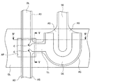
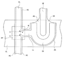
図1は、TFT基板上に実装される走査信号線GL、映像信号線DL、接続線LL、及び薄膜トランジスタTの位置関係を示すTFT基板上の部分平面図である。また、図2は、TFT基板上に実装される走査信号線GL、映像信号線DL、薄膜トランジスタT、画素電極PIT、コモン信号線CL、及びコモン電極CITの概略の回路構成を示す回路図である。さらに、図3は、TFT基板の1つの画素領域の平面図である。 FIG. 1 is a partial plan view on a TFT substrate showing the positional relationship among scanning signal lines GL, video signal lines DL, connection lines LL, and thin film transistors T mounted on the TFT substrate. FIG. 2 is a circuit diagram showing a schematic circuit configuration of the scanning signal line GL, the video signal line DL, the thin film transistor T, the pixel electrode PIT, the common signal line CL, and the common electrode CIT mounted on the TFT substrate. . Further, FIG. 3 is a plan view of one pixel region of the TFT substrate.
これらの図に示されるように、TFT基板上には、互いに平行な複数本の走査信号線GLが配置されている。また、複数本の映像信号線DLが、互いに平行に、かつ平面的に見た場合に複数本の走査信号線GLのそれぞれと略直交するように交差して配置されている。これらの走査信号線GLと映像信号線DLとによって、碁盤状に並ぶ画素のそれぞれが区画されており、走査信号線GLと映像信号線DLとが交差する箇所のそれぞれが、本実施形態に係る表示装置の画素に対応する。 As shown in these drawings, a plurality of scanning signal lines GL parallel to each other are arranged on the TFT substrate. Further, the plurality of video signal lines DL are arranged so as to intersect each of the plurality of scanning signal lines GL substantially orthogonally when viewed in parallel and in a plane. The scanning signal lines GL and the video signal lines DL define each of the pixels arranged in a grid pattern, and each of the locations where the scanning signal lines GL and the video signal lines DL intersect is related to the present embodiment. This corresponds to the pixel of the display device.
また、走査信号線GL及び映像信号線DLによって区画される複数の画素領域のそれぞれには、当該画素の表示制御を行うための薄膜トランジスタTが形成されている。薄膜トランジスタTのゲート電極は走査信号線GLの一部によって構成されており、ドレイン電極DEは接続線LLを介して映像信号線DLと接続され、ソース電極SEは画素電極PITと接続されている。一方、各画素電極PITと対応するコモン電極CITは、それぞれ走査信号線GLと平行に配置された複数本のコモン信号線CLのいずれかと接続される。なお、本実施形態ではドレイン電極DEがU字型形状を有しているが、ドレイン電極DEの形状は他の形状であってもよい。 In each of the plurality of pixel regions partitioned by the scanning signal line GL and the video signal line DL, a thin film transistor T for performing display control of the pixel is formed. The gate electrode of the thin film transistor T is constituted by a part of the scanning signal line GL, the drain electrode DE is connected to the video signal line DL via the connection line LL, and the source electrode SE is connected to the pixel electrode PIT. On the other hand, the common electrode CIT corresponding to each pixel electrode PIT is connected to one of the plurality of common signal lines CL arranged in parallel with the scanning signal line GL. In the present embodiment, the drain electrode DE has a U-shape, but the drain electrode DE may have another shape.
本実施形態に係る表示装置では、走査信号線駆動回路GDRによって、所定タイミングごとに走査信号線GLに選択的に電圧が印加され、映像信号線駆動回路DDRによって、所定タイミングごとに映像信号線DLに選択的に電圧が印加される。こうして、表示制御の対象となる画素電極に対応する薄膜トランジスタTのオン/オフが制御され、当該薄膜トランジスタTを介して表示対象の画素の画素電極PITに電圧が印加される。これにより、本実施形態に係る表示装置は、画素電極PITとコモン電極CITとの間に生じる電界によって液晶分子を制御して、画素ごとの表示制御を行う。ここで、画素電極PIT及びコモン電極CITは、いずれも透明電極膜であって、平面的に見た場合に互いにその少なくとも一部が重なるように配置されている。 In the display device according to the present embodiment, a voltage is selectively applied to the scanning signal line GL at every predetermined timing by the scanning signal line driving circuit GDR, and the video signal line DL at every predetermined timing by the video signal line driving circuit DDR. A voltage is selectively applied to. In this way, on / off of the thin film transistor T corresponding to the pixel electrode to be subjected to display control is controlled, and a voltage is applied to the pixel electrode PIT of the pixel to be displayed through the thin film transistor T. Accordingly, the display device according to the present embodiment performs display control for each pixel by controlling liquid crystal molecules by an electric field generated between the pixel electrode PIT and the common electrode CIT. Here, each of the pixel electrode PIT and the common electrode CIT is a transparent electrode film, and is arranged such that at least a part thereof overlaps each other when viewed in a plan view.
また、図1に示すように、走査信号線GL内の、走査信号線GLと映像信号線DLとが交差する箇所には、その一部が映像信号線DLと重なるように、開口部APが設けられている。そして、前述した接続線LLは、この開口部AP上で映像信号線DLから分岐して、開口部APの外まで(すなわち走査信号線GL上まで)伸びてからドレイン電極DEと接続されている。 Further, as shown in FIG. 1, in the scanning signal line GL, an opening AP is formed at a portion where the scanning signal line GL and the video signal line DL intersect so that a part thereof overlaps with the video signal line DL. Is provided. The connection line LL described above branches from the video signal line DL over the opening AP and extends to the outside of the opening AP (that is, up to the scanning signal line GL), and then is connected to the drain electrode DE. .
さらに、本実施形態に係る表示装置では、映像信号線DLから接続線LLが分岐する箇所に切欠部Cが形成されている。具体的には、映像信号線DL及び接続線LLによって形成される角から、映像信号線DL及び接続線LLの中心線の交点への方向と略等しい方向に向かって切り欠かれてなる切欠部Cが形成されている。この切欠部Cの役割については後述する。 Further, in the display device according to the present embodiment, a notch C is formed at a location where the connection line LL branches from the video signal line DL. Specifically, a notch formed by cutting out from a corner formed by the video signal line DL and the connection line LL in a direction substantially equal to the direction to the intersection of the center lines of the video signal line DL and the connection line LL. C is formed. The role of the notch C will be described later.
図4は、図1のIV−IV線におけるTFT基板の断面の様子を示す部分断面図であり、図5は、図1のV−V線におけるTFT基板の断面の様子を示す部分断面図である。図4及び図5に示すように、TFT基板TS上には、走査信号線GL、絶縁膜GI、半導体層AS、導電体層、及び保護膜PASが順次積層されている。ここで、導電体層は、映像信号線DL、接続線LL、ドレイン電極DE、及びソース電極SEを含んだ層である。なお、図4及び図5には示されていないが、コモン電極CIT及びコモン信号線CLが存在する領域では、TFT基板TS上にコモン電極CIT及びコモン信号線CLも形成される。また、画素電極PITが存在する領域では、保護膜PASの上の層にさらに画素電極PITがソース電極SEと接続するように形成される。 4 is a partial cross-sectional view showing a state of the cross section of the TFT substrate taken along line IV-IV in FIG. 1, and FIG. is there. As shown in FIGS. 4 and 5, the scanning signal line GL, the insulating film GI, the semiconductor layer AS, the conductor layer, and the protective film PAS are sequentially stacked on the TFT substrate TS. Here, the conductor layer is a layer including the video signal line DL, the connection line LL, the drain electrode DE, and the source electrode SE. Although not shown in FIGS. 4 and 5, in the region where the common electrode CIT and the common signal line CL exist, the common electrode CIT and the common signal line CL are also formed on the TFT substrate TS. In the region where the pixel electrode PIT exists, the pixel electrode PIT is further formed on the layer above the protective film PAS so as to be connected to the source electrode SE.
絶縁膜GIは、例えば窒化シリコンなどの材料を含んだ層であって、TFT基板TS上に形成された走査信号線GLを覆うように形成されている。半導体層ASは、例えばアモルファスシリコンなどの材料を含んだ層であって、図1に示されるように、平面的に観た場合に、絶縁膜GIの、導電体層が形成される領域より広がった領域を覆うように形成されている。すなわち、図4に示されるように、絶縁膜GIの、映像信号線DL、ドレイン電極DE、及びソース電極SEが形成される領域より広がった領域を覆うように半導体層ASは形成されている。また、図5に示されるように、絶縁膜GIの、接続線LLが形成される領域より広がった領域を覆うように半導体層ASは形成されている。 The insulating film GI is a layer containing a material such as silicon nitride, for example, and is formed so as to cover the scanning signal lines GL formed on the TFT substrate TS. The semiconductor layer AS is a layer containing a material such as amorphous silicon, for example. As shown in FIG. 1, the semiconductor layer AS expands from the region of the insulating film GI where the conductor layer is formed when viewed in a plan view. It is formed so as to cover the region. That is, as shown in FIG. 4, the semiconductor layer AS is formed so as to cover a region of the insulating film GI that is wider than a region where the video signal line DL, the drain electrode DE, and the source electrode SE are formed. Further, as shown in FIG. 5, the semiconductor layer AS is formed so as to cover the region of the insulating film GI that is wider than the region where the connection line LL is formed.
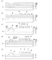
ここで、以上説明したような走査信号線GL、絶縁膜GI、半導体層AS、導電体層、及び保護膜PASを含んだ層が順次積層されたTFT基板TSを製造する方法について説明する。図6(a)〜(e)はこの製造方法について説明するための図であり、図4と同じ場所のTFT基板TSの断面の様子を示す部分断面図である。 Here, a method for manufacturing the TFT substrate TS in which the scanning signal line GL, the insulating film GI, the semiconductor layer AS, the conductor layer, and the layer including the protective film PAS as described above are sequentially stacked will be described. 6A to 6E are views for explaining the manufacturing method, and are partial cross-sectional views showing a cross-sectional state of the TFT substrate TS at the same place as that in FIG.
まず、フォトリソグラフィによって、走査信号線GLをTFT基板TSの基板面上に形成する。具体的には、TFT基板TS上に走査信号線GLを構成する材料の膜を形成し、その上にレジスト材の膜(レジスト膜)を積層して形成する。そして、露光及び現像によってレジスト膜を走査信号線GLの形状に対応するパターンに加工して、この加工されたレジスト膜をマスクとしてエッチングを行うことによって、走査信号線GLを形成する。その後、残っているレジスト膜を除去する。 First, the scanning signal lines GL are formed on the substrate surface of the TFT substrate TS by photolithography. Specifically, a film of a material constituting the scanning signal line GL is formed on the TFT substrate TS, and a film of a resist material (resist film) is stacked thereon. Then, the resist film is processed into a pattern corresponding to the shape of the scanning signal line GL by exposure and development, and etching is performed using the processed resist film as a mask, thereby forming the scanning signal line GL. Thereafter, the remaining resist film is removed.
次に、その状態のTFT基板TSの基板面上に、絶縁膜GI、半導体層ASを構成する半導体材料ASMの膜、及び導電体層を構成する導電体材料CDMの膜を、この順に順次積層して形成する。図6(a)は、この段階におけるTFT基板TSの断面の様子を示している。 Next, on the substrate surface of the TFT substrate TS in that state, the insulating film GI, the film of the semiconductor material ASM constituting the semiconductor layer AS, and the film of the conductor material CDM constituting the conductor layer are sequentially laminated in this order. To form. FIG. 6A shows a cross-sectional state of the TFT substrate TS at this stage.
さらに、図6(a)に示す状態のTFT基板TSにおいて、導電体材料CDMの膜の上にレジスト膜を形成する。そして、フォトリソグラフィによって、導電体層の形成を行う。具体的には、形成しようとする導電体層の形状に対応するマスクパターンを用いてレジスト膜の露光を行い、さらに現像処理を行うことによって、レジスト膜を導電体層の形状に対応するパターンに加工する。図6(b)は、この段階におけるTFT基板TSの断面の様子を示している。なお、本実施形態では、レジスト膜RFを露光する際のマスクパターンは、映像信号線DLから接続線LLが分岐する箇所に前述の切欠部Cが形成されるように設定される。 Further, in the TFT substrate TS in the state shown in FIG. 6A, a resist film is formed on the film of the conductor material CDM. Then, a conductor layer is formed by photolithography. Specifically, the resist film is exposed to light using a mask pattern corresponding to the shape of the conductor layer to be formed, and further developed to form a resist film in a pattern corresponding to the shape of the conductor layer. Process. FIG. 6B shows a cross-sectional state of the TFT substrate TS at this stage. In the present embodiment, the mask pattern for exposing the resist film RF is set so that the aforementioned notch C is formed at a location where the connection line LL branches from the video signal line DL.
次に、図6(b)に示す状態のTFT基板TSにおいて、上記の加工されたレジスト膜RFをマスクとして導電体材料CDMの膜をエッチングすることによって、映像信号線DL、接続線LL、ドレイン電極DE、及びソース電極SEを含んだ導電体層を形成する。図6(c)は、この段階におけるTFT基板TSの断面の様子を示している。 Next, in the TFT substrate TS in the state shown in FIG. 6B, the film of the conductor material CDM is etched by using the processed resist film RF as a mask, whereby the video signal line DL, the connection line LL, the drain A conductor layer including the electrode DE and the source electrode SE is formed. FIG. 6C shows a cross-sectional state of the TFT substrate TS at this stage.
続いて、導電体層が形成されて図6(c)に示す状態になった後に、導電体層上に残っているレジスト膜RFを加熱融解する。これにより、TFT基板TSを平面的に見た場合に、レジスト膜RFは、導電体層が形成された領域よりも広がった領域を覆うように広がった状態になる。図6(d)は、このレジスト膜RFが融解された状態のTFT基板TSの断面の様子を示している。 Subsequently, after the conductor layer is formed and the state shown in FIG. 6C is obtained, the resist film RF remaining on the conductor layer is heated and melted. As a result, when the TFT substrate TS is viewed in plan, the resist film RF is in a state of spreading so as to cover a region that is wider than the region where the conductor layer is formed. FIG. 6D shows the state of the cross section of the TFT substrate TS in a state where the resist film RF is melted.
この状態において、融解されたレジスト膜RFをマスクとして、半導体材料ASMの膜に対するエッチングを行う。その後、残っているレジスト膜RFを除去する。このようにすることによって、絶縁膜GIの、導電体層が形成される領域より広がった領域を覆うように、半導体層ASが形成される。図6(e)は、この段階におけるTFT基板TSの断面の様子を示している。なお、この状態において保護膜PASがさらに形成され、TFT基板TSは図4に示す状態になる。 In this state, the film of the semiconductor material ASM is etched using the melted resist film RF as a mask. Thereafter, the remaining resist film RF is removed. In this way, the semiconductor layer AS is formed so as to cover the region of the insulating film GI that is wider than the region where the conductor layer is formed. FIG. 6E shows the state of the cross section of the TFT substrate TS at this stage. In this state, the protective film PAS is further formed, and the TFT substrate TS is in the state shown in FIG.
ここで、レジスト膜RFの広がりは融解によって生じるため、レジスト膜RFに生じる表面張力の影響などにより、半導体層ASの導電体層からはみ出す領域の幅は均一にはならない。特に、融解されたレジスト膜RFは、映像信号線DLや接続線LLなどによって形成される角に集まりやすく、例えば、映像信号線DLから接続線LLが分岐する箇所などに集まりやすい。このため、図13に示されるように、映像信号線DLから接続線LLが分岐する箇所などでは、半導体層ASの広がりが大きくなりやすい。 Here, since the spread of the resist film RF is caused by melting, the width of the region protruding from the conductor layer of the semiconductor layer AS is not uniform due to the influence of the surface tension generated in the resist film RF. In particular, the melted resist film RF tends to gather at the corner formed by the video signal line DL, the connection line LL, etc., for example, easily gathers at a location where the connection line LL branches from the video signal line DL. For this reason, as shown in FIG. 13, the spread of the semiconductor layer AS tends to increase at a location where the connection line LL branches from the video signal line DL.
この点、本実施形態では、映像信号線DLから接続線LLが分岐する箇所に切欠部Cが形成されている。下記に説明するように、この切欠部Cは、半導体層ASを形成する工程において導電体層上に残っているレジスト膜RFを融解した場合の、開口部AP内におけるレジスト膜RFの広がりを制御する役割を果たす。 In this regard, in the present embodiment, a notch C is formed at a location where the connection line LL branches from the video signal line DL. As will be described below, the notch C controls the spread of the resist film RF in the opening AP when the resist film RF remaining on the conductor layer is melted in the process of forming the semiconductor layer AS. To play a role.
すなわち、本実施形態では、導電体層上に残っているレジスト膜RFを融解した場合、融解されたレジスト膜RFの一部が切欠部Cに流れ込むようになる。このため、映像信号線DLから接続線LLが分岐する箇所付近に本来は溜るはずであったレジスト膜RFの一部が切欠部C内に流れ込むようになり、映像信号線DLから接続線LLが分岐する箇所付近におけるレジスト膜RFの広がりが軽減される。その結果、半導体層ASが、接続線LLが配置される側の開口部APの大部分の領域を占めるように広がって形成されないようになる。本実施形態によれば、黒点化修正を行おうとする場合(接続線LLを切断しようとする場合)の場所的余裕が開口部AP内に確保されるようになる。また、開口部APによって二股に分岐した走査信号線GLのうち、映像信号線DLと短絡している方の走査信号線GLを切り離そうとする場合の場所的余裕も開口部AP内に確保されるようになる。 That is, in the present embodiment, when the resist film RF remaining on the conductor layer is melted, a part of the melted resist film RF flows into the notch C. For this reason, a part of the resist film RF that should originally have accumulated near the portion where the connection line LL branches from the video signal line DL flows into the notch C, and the connection line LL extends from the video signal line DL. The spread of the resist film RF in the vicinity of the branching point is reduced. As a result, the semiconductor layer AS is not formed so as to occupy the most area of the opening AP on the side where the connection line LL is disposed. According to the present embodiment, a spatial margin is secured in the opening AP when black spot correction is to be performed (when the connection line LL is to be disconnected). In addition, in the opening AP, a sufficient margin is secured in the opening AP when the scanning signal line GL that is short-circuited to the video signal line DL among the scanning signal lines GL branched into two by the opening AP is to be separated. Will come to be.
ところで、図1に示す例では、切欠部Cが映像信号線DL及び接続線LLの両方にまたがるようにして形成されている。しかしながら、切欠部Cは映像信号線DL又は接続線LLの一方に形成されるようにしてもよい。この場合、映像信号線DLから接続線LLが分岐する箇所付近に本来は溜るはずであったレジスト膜RFの一部が流れ込むような位置に、切欠部Cを形成するようにすればよい。例えば、開口部APに対応する領域内であって、かつ、映像信号線DLから接続線LLが分岐する箇所の近傍に切欠部Cを形成するようにすればよい。 By the way, in the example shown in FIG. 1, the notch C is formed so as to straddle both the video signal line DL and the connection line LL. However, the notch C may be formed in one of the video signal line DL or the connection line LL. In this case, the notch C may be formed at a position where a part of the resist film RF that should originally have accumulated near the portion where the connection line LL branches from the video signal line DL flows. For example, the cutout C may be formed in a region corresponding to the opening AP and in the vicinity of a portion where the connection line LL branches from the video signal line DL.
[第2実施形態]
第2実施形態に係る表示装置も第1実施形態と同様の構成(図2〜図5参照)を有し、第2実施形態におけるTFT基板TSの製造方法も第1実施形態と同様の製造方法(図6参照)であるため、ここでは説明を省略する。
[Second Embodiment]
The display device according to the second embodiment has the same configuration as that of the first embodiment (see FIGS. 2 to 5), and the manufacturing method of the TFT substrate TS in the second embodiment is the same as that of the first embodiment. (Refer to FIG. 6), and the description is omitted here.
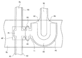
本実施形態に係る表示装置は、半導体層ASを形成する工程において導電体層上に残っているレジスト膜RFを融解した場合の、開口部AP内におけるレジスト膜RFの広がりを制御するための拡幅部が、映像信号線DL又は/及び接続線LLに設けられる点で、第1実施形態とは相違する。図7は、本実施形態に係る表示装置のTFT基板TSの部分平面図であり、第1実施形態における図1に対応する図である。 The display device according to the present embodiment has a widening for controlling the spread of the resist film RF in the opening AP when the resist film RF remaining on the conductor layer is melted in the step of forming the semiconductor layer AS. This is different from the first embodiment in that the unit is provided in the video signal line DL or / and the connection line LL. FIG. 7 is a partial plan view of the TFT substrate TS of the display device according to the present embodiment, and corresponds to FIG. 1 in the first embodiment.
図7に示すように、本実施形態に係る表示装置では、接続線LLの、映像信号線DLとの接続端から所定距離以内の領域において、映像信号線DLに近づくにつれて幅が徐々に広くなるような拡幅部Wが形成されている。この拡幅部Wが形成されることによって、映像信号線DLと接続線LLとが形成する角が比較的緩やかになっている。なお、この拡幅部Wは、接続線LLが配置される側の開口部APの全域が覆われてしまうことがないように、すなわち、接続線LLが配置される側の開口部APの一部のみが覆われるように形成される。 As shown in FIG. 7, in the display device according to the present embodiment, the width of the connection line LL gradually increases as it approaches the video signal line DL in a region within a predetermined distance from the connection end with the video signal line DL. Such a widened portion W is formed. By forming the widened portion W, the angle formed by the video signal line DL and the connection line LL is relatively gentle. The widened portion W is not covered with the entire opening AP on the side where the connection line LL is arranged, that is, a part of the opening AP on the side where the connection line LL is arranged. It is formed so that only it is covered.
なお、本実施形態では、導電体層を形成する工程(図6(b)参照)において、導電体材料CDM上に積層されたレジスト膜RFを露光する際のマスクパターンは、前述の拡幅部Wが接続線LLに形成されるように設定される。 In the present embodiment, in the step of forming the conductor layer (see FIG. 6B), the mask pattern used when exposing the resist film RF laminated on the conductor material CDM is the above-described widened portion W. Is formed on the connection line LL.
半導体層ASを形成する工程において導電体層上に残っているレジスト膜RFを融解した場合、映像信号線DLと接続線LLとが形成する角が鋭い程、映像信号線DLから接続線LLが分岐する箇所に、融解されたレジスト膜RFが集まりやすくなる。この点、本実施形態では、拡幅部Wが形成されていることによって、映像信号線DLと接続線LLと形成する角が比較的緩やかになるため、映像信号線DLから接続線LLが分岐する箇所に、融解されたレジスト膜RFが集まり難くなる。このため、映像信号線DLから接続線LLが分岐する箇所におけるレジスト膜RFの広がりが軽減され、半導体層ASが、接続線LLが配置される側の開口部APの大部分の領域を占めるように広がって形成されてしまわないようになる。本実施形態によっても、黒点化修正を行おうとする場合の場所的余裕が開口部AP内に確保されるようになる。また、開口部APによって二股に分岐した走査信号線GLのうち、映像信号線DLと短絡している方の走査信号線GLを切り離そうとする場合の場所的余裕も開口部AP内に確保されるようになる。 When the resist film RF remaining on the conductor layer is melted in the step of forming the semiconductor layer AS, the sharper the angle formed by the video signal line DL and the connection line LL, the more the connection line LL is connected from the video signal line DL. The melted resist film RF tends to gather at the branching location. In this regard, in the present embodiment, since the widened portion W is formed, the angle formed between the video signal line DL and the connection line LL becomes relatively gentle, so that the connection line LL branches from the video signal line DL. It is difficult for the melted resist film RF to gather at the location. For this reason, the spread of the resist film RF at the portion where the connection line LL branches from the video signal line DL is reduced, and the semiconductor layer AS occupies most of the region of the opening AP on the side where the connection line LL is disposed. It will not be formed to spread. Also according to the present embodiment, a spatial margin is secured in the opening AP when the black spot correction is to be performed. In addition, in the opening AP, a sufficient margin is secured in the opening AP when the scanning signal line GL that is short-circuited to the video signal line DL among the scanning signal lines GL branched into two by the opening AP is to be separated. Will come to be.
なお、図7に示す例では、映像信号線DLに拡幅部Wが形成されているともいうことができる。すなわち、接続線LLの分岐箇所に近づくにつれて幅が接続線LLの延伸方向に向かって徐々に広くなるような拡幅部Wが映像信号線DLに形成されているともいうことができる。また、拡幅部Wは映像信号線DLと接続線LLとにまたがって形成されているともいうことができる。 In the example shown in FIG. 7, it can be said that the widened portion W is formed in the video signal line DL. That is, it can be said that the widened portion W is formed in the video signal line DL such that the width gradually increases in the extending direction of the connection line LL as it approaches the branching point of the connection line LL. It can also be said that the widened portion W is formed across the video signal line DL and the connection line LL.
[第3実施形態]
第3実施形態に係る表示装置も第1実施形態と同様の構成(図2〜図5参照)を有し、第3実施形態におけるTFT基板TSの製造方法も第1実施形態と同様の製造方法(図6参照)であるため、ここでは説明を省略する。
[Third Embodiment]
The display device according to the third embodiment has the same configuration as that of the first embodiment (see FIGS. 2 to 5), and the manufacturing method of the TFT substrate TS in the third embodiment is the same as that of the first embodiment. (Refer to FIG. 6), and the description is omitted here.
本実施形態に係る表示装置は、半導体層ASを形成する工程において導電体層上に残っているレジスト膜RFを融解した場合の、開口部AP内におけるレジスト膜RFの広がりを制御するための突起部が映像信号線DLに設けられる点で、第1実施形態とは相違する。図8は、本実施形態に係る表示装置のTFT基板TSの部分平面図であり、第1実施形態における図1に対応する図である。 The display device according to the present embodiment has a protrusion for controlling the spread of the resist film RF in the opening AP when the resist film RF remaining on the conductor layer is melted in the step of forming the semiconductor layer AS. This is different from the first embodiment in that the unit is provided on the video signal line DL. FIG. 8 is a partial plan view of the TFT substrate TS of the display device according to this embodiment, and corresponds to FIG. 1 in the first embodiment.
図8に示すように、本実施形態に係る表示装置では、映像信号線DLの、接続線LLが接続される側とは反対側に突起部P1が形成されている。なお、本実施形態では、導電体層を形成する工程(図6(b)参照)において、導電体材料CDM上に積層されたレジスト膜RFを露光する際のマスクパターンは、前述の突起部P1が映像信号線DLに形成されるように設定される。 As shown in FIG. 8, in the display device according to the present embodiment, a projection P1 is formed on the opposite side of the video signal line DL from the side to which the connection line LL is connected. In the present embodiment, in the step of forming the conductor layer (see FIG. 6B), the mask pattern used when exposing the resist film RF laminated on the conductor material CDM is the above-described protrusion P1. Is formed on the video signal line DL.
本実施形態では、半導体層ASを形成する工程において導電体層上に残っているレジスト膜RFを融解した場合、融解されたレジスト膜RFが、突起部P1付近にも集まりやすくなる。このため、開口部APの接続線LLが配置される側の領域に本来流れ込むはずであったレジスト膜RFの一部が、開口部APの接続線LLが配置されない側の領域にも流れ込むようになる。その結果、開口部APの接続線LLが配置される側の領域へのレジスト膜RFの広がりが軽減されるようになり、半導体層ASが、接続線LLが配置される側の開口部APの大部分の領域を占めるように広がって形成されてしまわないようになる。本実施形態によっても、黒点化修正を行おうとする場合の場所的余裕が開口部AP内に確保されるようになる。また、開口部APによって二股に分岐した走査信号線GLのうち、映像信号線DLと短絡している方の走査信号線GLを切り離そうとする場合の場所的余裕も開口部AP内に確保されるようになる。 In the present embodiment, when the resist film RF remaining on the conductor layer is melted in the step of forming the semiconductor layer AS, the melted resist film RF is likely to gather near the protrusion P1. For this reason, a part of the resist film RF that should originally flow into the region on the side where the connection line LL of the opening AP is arranged flows into the region on the side where the connection line LL of the opening AP is not arranged. Become. As a result, the spread of the resist film RF to the region on the side where the connection line LL of the opening AP is disposed is reduced, and the semiconductor layer AS is formed on the side of the opening AP on the side where the connection line LL is disposed. It will not be formed so as to occupy most of the area. Also according to the present embodiment, a spatial margin is secured in the opening AP when the black spot correction is to be performed. In addition, in the opening AP, a sufficient margin is secured in the opening AP when the scanning signal line GL that is short-circuited to the video signal line DL among the scanning signal lines GL branched into two by the opening AP is to be separated. Will come to be.
なお、図8に示す例では、突起部P1が、接続線LLと映像信号線DLに対して線対称となるような位置に設けられているが、突起部P1の位置は、接続線LLと映像信号線DLに対して線対称となるような位置に限られない。突起部P1は、開口部APの接続線LLが配置される側の領域に本来流れ込むはずであったレジスト膜RFの一部が集まってくるような位置に形成するようにすればよい。例えば、映像信号線DLの、接続線LLが接続される側とは反対側であって、かつ、開口部APに対応する領域内又はその近傍の位置に、突起部P1を形成するようにすればよい。また、図8に示す例では、突起部P1の突起方向が、接続線LLの延伸方向と略正反対の方向になっているが、必ずしも、突起部P1の突起方向は、接続線LLの延伸方向と略正反対の方向に限られない。さらに、図8に示す例では、平面的に見た場合の突起部P1の幅が接続線LLの幅と略等しくなっているが、突起部P1の幅は接続線LLの幅と略等しくなくてもよい。 In the example shown in FIG. 8, the protrusion P1 is provided at a position that is symmetrical with respect to the connection line LL and the video signal line DL. However, the position of the protrusion P1 is the same as the connection line LL. The position is not limited to be symmetrical with respect to the video signal line DL. The protrusion P1 may be formed at a position where a part of the resist film RF that should originally flow into the region on the side where the connection line LL of the opening AP is arranged gathers. For example, the protrusion P1 is formed on the video signal line DL on the side opposite to the side to which the connection line LL is connected and in the region corresponding to the opening AP or in the vicinity thereof. That's fine. In the example shown in FIG. 8, the protruding direction of the protruding portion P1 is substantially opposite to the extending direction of the connection line LL. However, the protruding direction of the protruding portion P1 is not necessarily the extending direction of the connecting line LL. It is not limited to the opposite direction. Further, in the example shown in FIG. 8, the width of the protrusion P1 when viewed in plan is substantially equal to the width of the connection line LL, but the width of the protrusion P1 is not substantially equal to the width of the connection line LL. May be.
[第4実施形態]
第4実施形態に係る表示装置も第1実施形態と同様の構成(図2〜図5参照)を有し、第4実施形態におけるTFT基板TSの製造方法も第1実施形態と同様の製造方法(図6参照)であるため、ここでは説明を省略する。
[Fourth Embodiment]
The display device according to the fourth embodiment has the same configuration as that of the first embodiment (see FIGS. 2 to 5), and the manufacturing method of the TFT substrate TS in the fourth embodiment is the same as that of the first embodiment. (Refer to FIG. 6), and the description is omitted here.
本実施形態に係る表示装置は、半導体層ASを形成する工程において導電体層上に残っているレジスト膜RFを融解した場合の、開口部AP内におけるレジスト膜RFの広がりを制御するための突起部が接続線LLに設けられる点で、第1実施形態とは相違する。図9は、本実施形態に係る表示装置のTFT基板TSの部分平面図であり、第1実施形態における図1に対応する図である。 The display device according to the present embodiment has a protrusion for controlling the spread of the resist film RF in the opening AP when the resist film RF remaining on the conductor layer is melted in the step of forming the semiconductor layer AS. This is different from the first embodiment in that the portion is provided on the connection line LL. FIG. 9 is a partial plan view of the TFT substrate TS of the display device according to the present embodiment, and corresponds to FIG. 1 in the first embodiment.
図9に示すように、本実施形態に係る表示装置では、接続線LLの、開口部APに対応する領域より外側であって、かつ、開口部APの近傍の位置に突起部P2が形成されている。なお、本実施形態では、導電体層を形成する工程(図6(b)参照)において、導電体材料CDM上に積層されたレジスト膜RFを露光する際のマスクパターンは、前述の突起部P2が接続線LLに形成されるように設定される。 As shown in FIG. 9, in the display device according to the present embodiment, the protrusion P2 is formed at a position outside the region corresponding to the opening AP of the connection line LL and in the vicinity of the opening AP. ing. In the present embodiment, in the step of forming the conductor layer (see FIG. 6B), the mask pattern when exposing the resist film RF laminated on the conductor material CDM is the above-described protrusion P2. Is formed on the connection line LL.
半導体層ASを形成する工程において導電体層上に残っているレジスト膜RFを融解した場合、融解されたレジスト膜RFは、映像信号線DLや接続線LLなどによって形成される角に集まりやすい。この点、本実施形態では、前述の突起部P2が接続線LLに形成されているため、融解されたレジスト膜RFは突起部P2の付近にも集まりやすくなる。その結果、開口部APの接続線LLが配置される側の領域内に本来溜るはずであったレジスト膜RFの一部が、開口部AP外に溜るようになる。このため、開口部APの接続線LLが配置される側の領域におけるレジスト膜RFの広がりが軽減されるようになり、半導体層ASが、接続線LLが配置される側の開口部APの大部分の領域を占めるように広がって形成されてしまわないようになる。本実施形態によっても、黒点化修正を行おうとする場合の場所的余裕が開口部AP内に確保されるようになる。また、開口部APによって二股に分岐した走査信号線GLのうち、映像信号線DLと短絡している方の走査信号線GLを切り離そうとする場合の場所的余裕が開口部AP内に確保されるようになる。 When the resist film RF remaining on the conductor layer is melted in the process of forming the semiconductor layer AS, the melted resist film RF tends to gather at corners formed by the video signal lines DL, the connection lines LL, and the like. In this respect, in the present embodiment, since the above-described protrusion P2 is formed on the connection line LL, the melted resist film RF tends to gather near the protrusion P2. As a result, a part of the resist film RF that should have been accumulated in the region on the side where the connection line LL of the opening AP is disposed is accumulated outside the opening AP. For this reason, the spread of the resist film RF in the region on the side where the connection line LL of the opening AP is arranged is reduced, and the semiconductor layer AS is larger than the opening AP on the side where the connection line LL is arranged. It will not be formed so as to occupy a partial area. Also according to the present embodiment, a spatial margin is secured in the opening AP when the black spot correction is to be performed. In addition, a space is secured in the opening AP when the scanning signal line GL that is short-circuited to the video signal line DL among the scanning signal lines GL branched in two by the opening AP is to be disconnected. Will come to be.
なお、図9に示す例では、突起部P2の突起方向が、接続線LLの延伸方向と略直交する方向になっているが、必ずしも、突起部P2の突起方向は、接続線LLの延伸方向と略直交する方向に限られない。 In the example shown in FIG. 9, the protruding direction of the protruding portion P2 is substantially perpendicular to the extending direction of the connection line LL, but the protruding direction of the protruding portion P2 is not necessarily the extending direction of the connecting line LL. It is not restricted to the direction substantially orthogonal to.
[第5実施形態]
第5実施形態に係る表示装置も第1実施形態と同様の構成(図2〜図5参照)を有し、第5実施形態におけるTFT基板TSの製造方法も第1実施形態と同様の製造方法(図6参照)であるため、ここでは説明を省略する。
[Fifth Embodiment]
The display device according to the fifth embodiment has the same configuration as that of the first embodiment (see FIGS. 2 to 5), and the manufacturing method of the TFT substrate TS in the fifth embodiment is the same as that of the first embodiment. (Refer to FIG. 6), and the description is omitted here.
本実施形態に係る表示装置は、半導体層ASを形成する工程において導電体層上に残っているレジスト膜RFを融解した場合の、開口部AP内におけるレジスト膜RFの広がりを制御するための突起部が、映像信号線DLから接続線LLが分岐する箇所に形成される点で、第1実施形態とは相違する。図10は、本実施形態に係る表示装置のTFT基板TSの部分平面図であり、第1実施形態における図1に対応している。 The display device according to the present embodiment has a protrusion for controlling the spread of the resist film RF in the opening AP when the resist film RF remaining on the conductor layer is melted in the step of forming the semiconductor layer AS. This is different from the first embodiment in that the portion is formed at a location where the connection line LL branches from the video signal line DL. FIG. 10 is a partial plan view of the TFT substrate TS of the display device according to the present embodiment, and corresponds to FIG. 1 in the first embodiment.
図10に示すように、本実施形態に係る表示装置では、映像信号線DLから接続線LLが分岐する箇所に突起部P3が形成されている。なお、本実施形態では、導電体層を形成する工程(図6(b)参照)において、導電体材料CDM上に積層されたレジスト膜RFを露光する際のマスクパターンは、映像信号線DLから接続線LLが分岐する箇所に前述の突起部P3が形成されるように設定される。 As shown in FIG. 10, in the display device according to the present embodiment, the protrusion P3 is formed at a location where the connection line LL branches from the video signal line DL. In the present embodiment, in the step of forming the conductor layer (see FIG. 6B), the mask pattern for exposing the resist film RF laminated on the conductor material CDM is from the video signal line DL. It is set so that the above-described protrusion P3 is formed at a location where the connection line LL branches.
半導体層ASを形成する工程において導電体層上に残っているレジスト膜RFを融解した場合、融解されたレジスト膜RFは、映像信号線DLや接続線LLなどによって形成される角に集まりやすい。この点、本実施形態では、映像信号線DLから接続線LLが分岐する箇所に突起部P3が設けられているため、融解されたレジスト膜RFは、映像信号線DLから接続線LLが分岐する箇所に、より集まりやすくなる。すなわち、開口部APの接続線LLが配置される側の領域に広がるはずであったレジスト膜RFが、映像信号線DLから接続線LLが分岐する箇所に、より集中するようになる。その結果、開口部APの接続線LLが配置される側の領域におけるレジスト膜RFの広がりが軽減され、半導体層ASが、接続線LLが配置される側の開口部APの大部分の領域を占めるように広がって形成されてしまわないようになる。本実施形態によっても、黒点化修正を行おうとする場合の場所的余裕が開口部AP内に確保されるようになる。また、開口部APによって二股に分岐した走査信号線GLのうち、映像信号線DLと短絡している方の走査信号線GLを切り離そうとする場合の場所的余裕も開口部AP内に確保されるようになる。 When the resist film RF remaining on the conductor layer is melted in the process of forming the semiconductor layer AS, the melted resist film RF tends to gather at corners formed by the video signal lines DL, the connection lines LL, and the like. In this regard, in the present embodiment, since the projection P3 is provided at a location where the connection line LL branches from the video signal line DL, the melted resist film RF branches from the video signal line DL to the connection line LL. It becomes easier to gather in places. That is, the resist film RF that should have spread in the region on the side where the connection line LL of the opening AP is arranged is more concentrated at the location where the connection line LL branches from the video signal line DL. As a result, the spread of the resist film RF in the region on the side where the connection line LL of the opening AP is disposed is reduced, and the semiconductor layer AS covers most of the region of the opening AP on the side where the connection line LL is disposed. It will not be formed so as to occupy. Also according to the present embodiment, a spatial margin is secured in the opening AP when the black spot correction is to be performed. In addition, in the opening AP, a sufficient margin is secured in the opening AP when the scanning signal line GL that is short-circuited to the video signal line DL among the scanning signal lines GL branched into two by the opening AP is to be separated. Will come to be.
なお、本発明は以上に説明した実施の形態に限定されるものではない。 The present invention is not limited to the embodiment described above.
例えば、第1〜5実施形態のうちの複数を組み合わせるようにしてもよい。図11は、第1実施形態と第2実施形態とを組み合わせた例を示しており、図12は、第3実施形態と第4実施形態とを組み合わせた例を示している。このようにすれば、導電体層上に残っているレジスト膜RFを融解した場合の、開口部APの接続線LLが配置される側の領域におけるレジスト膜RFの広がりをさらに軽減できるようになる。 For example, a plurality of the first to fifth embodiments may be combined. FIG. 11 shows an example in which the first embodiment and the second embodiment are combined, and FIG. 12 shows an example in which the third embodiment and the fourth embodiment are combined. In this case, when the resist film RF remaining on the conductor layer is melted, the spread of the resist film RF in the region on the side where the connection line LL of the opening AP is disposed can be further reduced. .
また例えば、以上では、いわゆるIPS方式の液晶表示装置に本発明を適用した場合の例について説明した。すなわち、TFT基板TS上に形成された画素電極PIT及びコモン電極CITの間に生じる横方向の電界によって、液晶分子の制御を行う方式を採用した表示装置に本発明を適用した場合の例について説明した。しかしながら、本発明は、他の方式を採用する表示装置にも適用することが可能である。例えば、本発明は、いわゆるVA(Virtical Alignment)方式の液晶表示装置にも適用することが可能である。すなわち、TFT基板TSの画素電極PITと、フィルタ基板の対抗電極と、の間に生じる縦方向の電界によって、液晶分子の制御を行う方式を採用した液晶表示装置にも本発明は適用することができる。また例えば、本発明は、いわゆるTN(Twisted Nematic)方式の液晶表示装置にも適用することが可能である。さらに、例えば、本発明は液晶表示装置以外の表示装置にも適用することができる。例えば有機EL表示装置等の他の表示装置においても、画素ごとに薄膜トランジスタが形成される場合には、前述した課題と同様の課題が生じ得るからである。 Further, for example, the example in which the present invention is applied to a so-called IPS liquid crystal display device has been described above. That is, an example in which the present invention is applied to a display device that adopts a method of controlling liquid crystal molecules by a horizontal electric field generated between the pixel electrode PIT and the common electrode CIT formed on the TFT substrate TS will be described. did. However, the present invention can also be applied to display devices that employ other methods. For example, the present invention can be applied to a so-called VA (Virtical Alignment) liquid crystal display device. That is, the present invention can also be applied to a liquid crystal display device adopting a method in which liquid crystal molecules are controlled by a vertical electric field generated between the pixel electrode PIT of the TFT substrate TS and the counter electrode of the filter substrate. it can. Further, for example, the present invention can be applied to a so-called TN (Twisted Nematic) liquid crystal display device. Furthermore, for example, the present invention can be applied to display devices other than liquid crystal display devices. For example, in other display devices such as an organic EL display device, when a thin film transistor is formed for each pixel, the same problem as described above may occur.
AP 開口部、AS 半導体層、ASM 半導体材料、C 切欠部、CDM 導電体材料、CIT コモン電極、CL コモン信号線、DDR 映像信号線駆動回路、DE ドレイン電極、DL 映像信号線、GDR 走査信号線駆動回路、GI 絶縁膜、GL 走査信号線、LL 接続線、P1,P2,P3 突起部、PAS 保護膜、PIT 画素電極、RF レジスト膜、SE ソース電極、T 薄膜トランジスタ、TS TFT基板、W 拡幅部。 AP opening, AS semiconductor layer, ASM semiconductor material, C notch, CDM conductor material, CIT common electrode, CL common signal line, DDR video signal line drive circuit, DE drain electrode, DL video signal line, GDR scanning signal line Drive circuit, GI insulating film, GL scanning signal line, LL connection line, P1, P2, P3 protrusion, PAS protective film, PIT pixel electrode, RF resist film, SE source electrode, T thin film transistor, TS TFT substrate, W widened portion .
Claims (12)
前記導電体層は、前記走査信号線と前記絶縁膜を介して交差する映像信号線と、薄膜トランジスタのドレイン電極及びソース電極と、前記映像信号線と前記ドレイン電極又は前記ソース電極のいずれか一方とを接続する接続線と、を含んで形成され、
前記半導体層は、少なくとも、前記絶縁膜の、前記映像信号線及び前記接続線が形成される領域より広がった領域を覆うように形成され、
前記走査信号線には、開口部が、前記映像信号線の一部と重なるように形成され、
前記接続線は、前記開口部上において前記映像信号線と接続され、かつ、前記開口部外に延伸して前記ドレイン電極又は前記ソース電極のいずれか一方と接続され、
前記映像信号線又は/及び前記接続線には、前記開口部に対応する領域又はその近傍において、切欠部、突起部又は拡幅部が形成されている、
ことを特徴とする表示装置。 A display device comprising a scanning signal line, an insulating film, a semiconductor layer, and a conductor layer sequentially stacked on a substrate,
The conductor layer includes a video signal line intersecting the scanning signal line through the insulating film, a drain electrode and a source electrode of a thin film transistor, and the video signal line and one of the drain electrode and the source electrode. Connecting wire, and including,
The semiconductor layer is formed so as to cover at least a region of the insulating film that is wider than a region where the video signal line and the connection line are formed,
The scanning signal line is formed so that an opening overlaps a part of the video signal line,
The connection line is connected to the video signal line on the opening, and extends to the outside of the opening and is connected to either the drain electrode or the source electrode.
In the video signal line or / and the connection line, a notch, a protrusion, or a widened portion is formed in a region corresponding to the opening or in the vicinity thereof.
A display device characterized by that.
前記導電体層が形成された後、前記導電体層上に残っている前記レジスト材を融解し、該融解された前記レジスト材をマスクとして前記半導体材料をエッチングすることによって、前記半導体層を形成する工程と、
を含み、
前記走査信号線には、開口部が、前記映像信号線の一部と重なるように形成され、
前記接続線は、前記開口部上において前記映像信号線と接続され、かつ、前記開口部外に延伸して前記ドレイン電極又は前記ソース電極のいずれか一方と接続され、
前記レジスト材は、前記レジスト材を融解した場合の、前記開口部における前記レジスト材の広がりを制御するための切欠部、突起部又は拡幅部を前記映像信号線又は/及び前記接続線が備えるようにパターン形成される、
ことを特徴とする表示装置の製造方法。 A resist material patterned on a laminated structure in which a scanning signal line, an insulating film, a semiconductor material constituting a semiconductor layer, and a conductor material constituting a conductor layer are sequentially laminated on a substrate. By etching the conductive material as a mask, a video signal line intersecting the scanning signal line through the insulating film, a drain electrode and a source electrode of a thin film transistor, the video signal line and the drain electrode or the source A step of forming the conductor layer including a connection line connecting any one of the electrodes;
After the conductor layer is formed, the semiconductor material is formed by melting the resist material remaining on the conductor layer and etching the semiconductor material using the melted resist material as a mask And a process of
Including
The scanning signal line is formed so that an opening overlaps a part of the video signal line,
The connection line is connected to the video signal line on the opening, and extends to the outside of the opening and is connected to either the drain electrode or the source electrode.
The video signal line and / or the connection line includes a notch, a protrusion, or a widened portion for controlling the spread of the resist material in the opening when the resist material is melted. To be patterned,
A manufacturing method of a display device characterized by the above.
Priority Applications (2)
| Application Number | Priority Date | Filing Date | Title |
|---|---|---|---|
| JP2008114683A JP5113609B2 (en) | 2008-04-24 | 2008-04-24 | Display device and manufacturing method thereof |
| US12/429,244 US8059077B2 (en) | 2008-04-24 | 2009-04-24 | Display device and manufacturing method of display device |
Applications Claiming Priority (1)
| Application Number | Priority Date | Filing Date | Title |
|---|---|---|---|
| JP2008114683A JP5113609B2 (en) | 2008-04-24 | 2008-04-24 | Display device and manufacturing method thereof |
Publications (3)
| Publication Number | Publication Date |
|---|---|
| JP2009265348A JP2009265348A (en) | 2009-11-12 |
| JP2009265348A5 JP2009265348A5 (en) | 2010-08-19 |
| JP5113609B2 true JP5113609B2 (en) | 2013-01-09 |
Family
ID=41379156
Family Applications (1)
| Application Number | Title | Priority Date | Filing Date |
|---|---|---|---|
| JP2008114683A Active JP5113609B2 (en) | 2008-04-24 | 2008-04-24 | Display device and manufacturing method thereof |
Country Status (2)
| Country | Link |
|---|---|
| US (1) | US8059077B2 (en) |
| JP (1) | JP5113609B2 (en) |
Families Citing this family (6)
| Publication number | Priority date | Publication date | Assignee | Title |
|---|---|---|---|---|
| US9568794B2 (en) | 2010-12-20 | 2017-02-14 | Semiconductor Energy Laboratory Co., Ltd. | Display device |
| CN103137558B (en) * | 2013-02-06 | 2016-10-05 | 京东方科技集团股份有限公司 | A kind of TN type array base palte and preparation method thereof, display device |
| JP6278633B2 (en) * | 2013-07-26 | 2018-02-14 | 三菱電機株式会社 | Thin film transistor array substrate and manufacturing method thereof, and liquid crystal display device and manufacturing method thereof |
| US10539839B2 (en) | 2015-02-12 | 2020-01-21 | Semiconductor Energy Laboratory Co., Ltd. | Display device |
| CN105405852B (en) * | 2016-01-05 | 2019-04-23 | 京东方科技集团股份有限公司 | Array substrate, method for manufacturing the same, and display device |
| CN109473449A (en) * | 2018-11-07 | 2019-03-15 | 惠科股份有限公司 | Overline structure, manufacturing method thereof and display panel |
Family Cites Families (9)
| Publication number | Priority date | Publication date | Assignee | Title |
|---|---|---|---|---|
| JP2762820B2 (en) * | 1992-02-21 | 1998-06-04 | 株式会社日立製作所 | Thin film transistor matrix and liquid crystal display device using the same |
| JPH08146462A (en) * | 1994-11-18 | 1996-06-07 | Hitachi Ltd | Liquid crystal display device and manufacturing method thereof |
| JPH09258244A (en) | 1996-03-22 | 1997-10-03 | Hitachi Ltd | Liquid crystal display |
| JPH10221704A (en) * | 1997-02-07 | 1998-08-21 | Sharp Corp | Reflective liquid crystal display device and method of manufacturing the same |
| JP3335567B2 (en) * | 1997-10-17 | 2002-10-21 | シャープ株式会社 | Active matrix type liquid crystal display device and its defect repair method |
| JP4211250B2 (en) * | 2000-10-12 | 2009-01-21 | セイコーエプソン株式会社 | Transistor and display device including the same |
| JP4410951B2 (en) * | 2001-02-27 | 2010-02-10 | Nec液晶テクノロジー株式会社 | Pattern forming method and manufacturing method of liquid crystal display device |
| US7858415B2 (en) * | 2005-04-28 | 2010-12-28 | Sharp Kabushiki Kaisha | Production methods of pattern thin film, semiconductor element, and circuit substrate, and resist material, semiconductor element, and circuit substrate |
| US7330235B2 (en) * | 2005-11-08 | 2008-02-12 | Chunghwa Picture Tubes, Ltd. | Liquid crystal display panel having spacers wedged in three-layered conductive lines and manufacturing method thereof |
-
2008
- 2008-04-24 JP JP2008114683A patent/JP5113609B2/en active Active
-
2009
- 2009-04-24 US US12/429,244 patent/US8059077B2/en active Active
Also Published As
| Publication number | Publication date |
|---|---|
| JP2009265348A (en) | 2009-11-12 |
| US8059077B2 (en) | 2011-11-15 |
| US20090295696A1 (en) | 2009-12-03 |
Similar Documents
| Publication | Publication Date | Title |
|---|---|---|
| KR101294237B1 (en) | Array substrate for fringe field switching mode liquid crystal display device and method of fabricating the same | |
| KR20080107821A (en) | Array substrate for fringe field switching mode liquid crystal display and manufacturing method thereof | |
| CN102096251A (en) | Active matrix substrate and liquid crystal display device provided with same | |
| JP4693781B2 (en) | Active matrix substrate and display device | |
| KR101634635B1 (en) | Display | |
| JP5113609B2 (en) | Display device and manufacturing method thereof | |
| JP2010079075A (en) | Transparent type liquid crystal display apparatus | |
| JP4644179B2 (en) | Array substrate for liquid crystal display device and manufacturing method thereof | |
| KR20140122623A (en) | Thin film transistor array panel and manufacturing method thereof | |
| US8309959B2 (en) | Display device having opening portion with different widths | |
| JP2009093176A (en) | Liquid crystal display device | |
| KR20140053667A (en) | Thin film transistor array substrate and manufacturing method thereof | |
| JP2010074030A (en) | Thin film transistor and electro-optic device | |
| KR20110072042A (en) | Liquid crystal display device and method for manufacturing same | |
| CN110176429B (en) | Method for manufacturing an array substrate, array substrate, and display panel | |
| TW201523103A (en) | Liquid crystal display and manufacturing method thereof | |
| KR101875937B1 (en) | Liquid crystal display device | |
| KR20120015162A (en) | Liquid crystal display device and manufacturing method thereof | |
| JP6234232B2 (en) | Liquid crystal display panel and repair method thereof | |
| JP5081461B2 (en) | Manufacturing method of display device | |
| JP2009271105A (en) | Method for manufacturing liquid crystal display device | |
| KR20090073709A (en) | Manufacturing method of array substrate for CIO structure transverse electric field liquid crystal display device | |
| JP2008089646A (en) | Display device | |
| JP2004333673A (en) | Display device | |
| JP2008170987A (en) | In-plane switching type liquid crystal display device |
Legal Events
| Date | Code | Title | Description |
|---|---|---|---|
| A521 | Request for written amendment filed |
Free format text: JAPANESE INTERMEDIATE CODE: A523 Effective date: 20100706 |
|
| A621 | Written request for application examination |
Free format text: JAPANESE INTERMEDIATE CODE: A621 Effective date: 20100706 |
|
| A977 | Report on retrieval |
Free format text: JAPANESE INTERMEDIATE CODE: A971007 Effective date: 20120907 |
|
| TRDD | Decision of grant or rejection written | ||
| A01 | Written decision to grant a patent or to grant a registration (utility model) |
Free format text: JAPANESE INTERMEDIATE CODE: A01 Effective date: 20120918 |
|
| A01 | Written decision to grant a patent or to grant a registration (utility model) |
Free format text: JAPANESE INTERMEDIATE CODE: A01 |
|
| A61 | First payment of annual fees (during grant procedure) |
Free format text: JAPANESE INTERMEDIATE CODE: A61 Effective date: 20121012 |
|
| FPAY | Renewal fee payment (event date is renewal date of database) |
Free format text: PAYMENT UNTIL: 20151019 Year of fee payment: 3 |
|
| R150 | Certificate of patent or registration of utility model |
Ref document number: 5113609 Country of ref document: JP Free format text: JAPANESE INTERMEDIATE CODE: R150 Free format text: JAPANESE INTERMEDIATE CODE: R150 |
|
| R250 | Receipt of annual fees |
Free format text: JAPANESE INTERMEDIATE CODE: R250 |
|
| R250 | Receipt of annual fees |
Free format text: JAPANESE INTERMEDIATE CODE: R250 |
|
| R250 | Receipt of annual fees |
Free format text: JAPANESE INTERMEDIATE CODE: R250 |
|
| R250 | Receipt of annual fees |
Free format text: JAPANESE INTERMEDIATE CODE: R250 |
|
| R250 | Receipt of annual fees |
Free format text: JAPANESE INTERMEDIATE CODE: R250 |
|
| R250 | Receipt of annual fees |
Free format text: JAPANESE INTERMEDIATE CODE: R250 |
|
| R250 | Receipt of annual fees |
Free format text: JAPANESE INTERMEDIATE CODE: R250 |
|
| R250 | Receipt of annual fees |
Free format text: JAPANESE INTERMEDIATE CODE: R250 |
|
| S111 | Request for change of ownership or part of ownership |
Free format text: JAPANESE INTERMEDIATE CODE: R313113 |
|
| R350 | Written notification of registration of transfer |
Free format text: JAPANESE INTERMEDIATE CODE: R350 |
|
| R250 | Receipt of annual fees |
Free format text: JAPANESE INTERMEDIATE CODE: R250 |
|
| R250 | Receipt of annual fees |
Free format text: JAPANESE INTERMEDIATE CODE: R250 |
|
| R250 | Receipt of annual fees |
Free format text: JAPANESE INTERMEDIATE CODE: R250 |