JP6202972B2 - Memory system and reading calibration method thereof - Google Patents
Memory system and reading calibration method thereof Download PDFInfo
- Publication number
- JP6202972B2 JP6202972B2 JP2013210121A JP2013210121A JP6202972B2 JP 6202972 B2 JP6202972 B2 JP 6202972B2 JP 2013210121 A JP2013210121 A JP 2013210121A JP 2013210121 A JP2013210121 A JP 2013210121A JP 6202972 B2 JP6202972 B2 JP 6202972B2
- Authority
- JP
- Japan
- Prior art keywords
- memory
- data
- read
- controller
- memory cells
- Prior art date
- Legal status (The legal status is an assumption and is not a legal conclusion. Google has not performed a legal analysis and makes no representation as to the accuracy of the status listed.)
- Active
Links
- 230000015654 memory Effects 0.000 title claims description 558
- 238000000034 method Methods 0.000 title claims description 74
- 230000008569 process Effects 0.000 claims description 21
- 230000008672 reprogramming Effects 0.000 claims description 11
- 238000012937 correction Methods 0.000 claims description 8
- 239000000872 buffer Substances 0.000 description 54
- 238000010586 diagram Methods 0.000 description 37
- 239000004065 semiconductor Substances 0.000 description 26
- 238000012795 verification Methods 0.000 description 11
- 238000001514 detection method Methods 0.000 description 6
- 238000005516 engineering process Methods 0.000 description 5
- 238000012545 processing Methods 0.000 description 5
- 238000003491 array Methods 0.000 description 4
- 238000004891 communication Methods 0.000 description 4
- 238000013507 mapping Methods 0.000 description 3
- 238000012986 modification Methods 0.000 description 3
- 230000004048 modification Effects 0.000 description 3
- 230000004044 response Effects 0.000 description 3
- 238000004519 manufacturing process Methods 0.000 description 2
- 238000012546 transfer Methods 0.000 description 2
- 239000003990 capacitor Substances 0.000 description 1
- 239000000919 ceramic Substances 0.000 description 1
- 230000008859 change Effects 0.000 description 1
- 239000000470 constituent Substances 0.000 description 1
- 230000008878 coupling Effects 0.000 description 1
- 238000010168 coupling process Methods 0.000 description 1
- 238000005859 coupling reaction Methods 0.000 description 1
- 238000013500 data storage Methods 0.000 description 1
- 238000013461 design Methods 0.000 description 1
- 238000011161 development Methods 0.000 description 1
- 230000018109 developmental process Effects 0.000 description 1
- 230000009977 dual effect Effects 0.000 description 1
- 238000000802 evaporation-induced self-assembly Methods 0.000 description 1
- 238000007667 floating Methods 0.000 description 1
- 230000006870 function Effects 0.000 description 1
- 230000010354 integration Effects 0.000 description 1
- 238000004377 microelectronic Methods 0.000 description 1
- 230000002093 peripheral effect Effects 0.000 description 1
- 230000003068 static effect Effects 0.000 description 1
- 238000013519 translation Methods 0.000 description 1
Images


Classifications
-
- G—PHYSICS
- G11—INFORMATION STORAGE
- G11C—STATIC STORES
- G11C16/00—Erasable programmable read-only memories
- G11C16/02—Erasable programmable read-only memories electrically programmable
- G11C16/06—Auxiliary circuits, e.g. for writing into memory
-
- G—PHYSICS
- G06—COMPUTING; CALCULATING OR COUNTING
- G06F—ELECTRIC DIGITAL DATA PROCESSING
- G06F11/00—Error detection; Error correction; Monitoring
- G06F11/07—Responding to the occurrence of a fault, e.g. fault tolerance
- G06F11/08—Error detection or correction by redundancy in data representation, e.g. by using checking codes
- G06F11/10—Adding special bits or symbols to the coded information, e.g. parity check, casting out 9's or 11's
- G06F11/1008—Adding special bits or symbols to the coded information, e.g. parity check, casting out 9's or 11's in individual solid state devices
- G06F11/1068—Adding special bits or symbols to the coded information, e.g. parity check, casting out 9's or 11's in individual solid state devices in sector programmable memories, e.g. flash disk
-
- G—PHYSICS
- G06—COMPUTING; CALCULATING OR COUNTING
- G06F—ELECTRIC DIGITAL DATA PROCESSING
- G06F11/00—Error detection; Error correction; Monitoring
- G06F11/07—Responding to the occurrence of a fault, e.g. fault tolerance
- G06F11/08—Error detection or correction by redundancy in data representation, e.g. by using checking codes
- G06F11/10—Adding special bits or symbols to the coded information, e.g. parity check, casting out 9's or 11's
- G06F11/1008—Adding special bits or symbols to the coded information, e.g. parity check, casting out 9's or 11's in individual solid state devices
- G06F11/1072—Adding special bits or symbols to the coded information, e.g. parity check, casting out 9's or 11's in individual solid state devices in multilevel memories
-
- G—PHYSICS
- G06—COMPUTING; CALCULATING OR COUNTING
- G06F—ELECTRIC DIGITAL DATA PROCESSING
- G06F12/00—Accessing, addressing or allocating within memory systems or architectures
- G06F12/02—Addressing or allocation; Relocation
- G06F12/0223—User address space allocation, e.g. contiguous or non contiguous base addressing
- G06F12/023—Free address space management
- G06F12/0238—Memory management in non-volatile memory, e.g. resistive RAM or ferroelectric memory
- G06F12/0246—Memory management in non-volatile memory, e.g. resistive RAM or ferroelectric memory in block erasable memory, e.g. flash memory
-
- G—PHYSICS
- G06—COMPUTING; CALCULATING OR COUNTING
- G06F—ELECTRIC DIGITAL DATA PROCESSING
- G06F12/00—Accessing, addressing or allocating within memory systems or architectures
- G06F12/02—Addressing or allocation; Relocation
- G06F12/0223—User address space allocation, e.g. contiguous or non contiguous base addressing
- G06F12/023—Free address space management
- G06F12/0253—Garbage collection, i.e. reclamation of unreferenced memory
-
- G—PHYSICS
- G11—INFORMATION STORAGE
- G11C—STATIC STORES
- G11C11/00—Digital stores characterised by the use of particular electric or magnetic storage elements; Storage elements therefor
- G11C11/56—Digital stores characterised by the use of particular electric or magnetic storage elements; Storage elements therefor using storage elements with more than two stable states represented by steps, e.g. of voltage, current, phase, frequency
- G11C11/5621—Digital stores characterised by the use of particular electric or magnetic storage elements; Storage elements therefor using storage elements with more than two stable states represented by steps, e.g. of voltage, current, phase, frequency using charge storage in a floating gate
- G11C11/5628—Programming or writing circuits; Data input circuits
-
- G—PHYSICS
- G11—INFORMATION STORAGE
- G11C—STATIC STORES
- G11C11/00—Digital stores characterised by the use of particular electric or magnetic storage elements; Storage elements therefor
- G11C11/56—Digital stores characterised by the use of particular electric or magnetic storage elements; Storage elements therefor using storage elements with more than two stable states represented by steps, e.g. of voltage, current, phase, frequency
- G11C11/5621—Digital stores characterised by the use of particular electric or magnetic storage elements; Storage elements therefor using storage elements with more than two stable states represented by steps, e.g. of voltage, current, phase, frequency using charge storage in a floating gate
- G11C11/5642—Sensing or reading circuits; Data output circuits
-
- G—PHYSICS
- G11—INFORMATION STORAGE
- G11C—STATIC STORES
- G11C11/00—Digital stores characterised by the use of particular electric or magnetic storage elements; Storage elements therefor
- G11C11/56—Digital stores characterised by the use of particular electric or magnetic storage elements; Storage elements therefor using storage elements with more than two stable states represented by steps, e.g. of voltage, current, phase, frequency
- G11C11/5671—Digital stores characterised by the use of particular electric or magnetic storage elements; Storage elements therefor using storage elements with more than two stable states represented by steps, e.g. of voltage, current, phase, frequency using charge trapping in an insulator
-
- G—PHYSICS
- G11—INFORMATION STORAGE
- G11C—STATIC STORES
- G11C16/00—Erasable programmable read-only memories
- G11C16/02—Erasable programmable read-only memories electrically programmable
- G11C16/06—Auxiliary circuits, e.g. for writing into memory
- G11C16/10—Programming or data input circuits
-
- G—PHYSICS
- G11—INFORMATION STORAGE
- G11C—STATIC STORES
- G11C16/00—Erasable programmable read-only memories
- G11C16/02—Erasable programmable read-only memories electrically programmable
- G11C16/06—Auxiliary circuits, e.g. for writing into memory
- G11C16/26—Sensing or reading circuits; Data output circuits
-
- G—PHYSICS
- G11—INFORMATION STORAGE
- G11C—STATIC STORES
- G11C16/00—Erasable programmable read-only memories
- G11C16/02—Erasable programmable read-only memories electrically programmable
- G11C16/06—Auxiliary circuits, e.g. for writing into memory
- G11C16/34—Determination of programming status, e.g. threshold voltage, overprogramming or underprogramming, retention
-
- G—PHYSICS
- G11—INFORMATION STORAGE
- G11C—STATIC STORES
- G11C29/00—Checking stores for correct operation ; Subsequent repair; Testing stores during standby or offline operation
- G11C29/52—Protection of memory contents; Detection of errors in memory contents
Landscapes
- Engineering & Computer Science (AREA)
- Theoretical Computer Science (AREA)
- Physics & Mathematics (AREA)
- General Engineering & Computer Science (AREA)
- General Physics & Mathematics (AREA)
- Computer Hardware Design (AREA)
- Quality & Reliability (AREA)
- Read Only Memory (AREA)
- Techniques For Improving Reliability Of Storages (AREA)
- Memory System (AREA)
Description
本発明は、半導体メモリ装置に係り、さらに具体的には、不揮発性メモリ装置を含むメモリシステムに関する。 The present invention relates to a semiconductor memory device, and more particularly to a memory system including a nonvolatile memory device.
半導体メモリは、一般的に、衛星から消費者電子技術までの範囲に属するマイクロプロセッサに基づいたアプリケーション及びコンピュータのようなデジタルロジック設計の最も必須的なマイクロ電子素子である。したがって、高集積度と高速な動作速度のための縮小(scaling)を通じて得られるプロセスの向上及び技術開発を含んだ半導体メモリの製造技術の進歩は、他のデジタルロジック系列の性能基準を確立するのに役立つ。 Semiconductor memory is generally the most essential microelectronic element in digital logic designs such as microprocessor-based applications and computers that range from satellites to consumer electronics. Therefore, advances in semiconductor memory manufacturing technology, including process improvements and technological developments obtained through scaling for high integration and high operating speed, will establish performance standards for other digital logic families. To help.
半導体メモリ装置は、大きく、揮発性半導体メモリ装置と不揮発性半導体メモリ装置とに分けられる。揮発性半導体メモリ装置において、ロジック情報は、スタティックRAMの場合、双安定フリップフロップのロジック状態を設定することにより、またはダイナミックランダムアクセスメモリの場合、キャパシタの充電を通じて格納される。揮発性半導体メモリ装置の場合、電源が印加される間、データが格納されて読み出され、電源が遮断されれば、データを失う。 Semiconductor memory devices are roughly classified into volatile semiconductor memory devices and non-volatile semiconductor memory devices. In a volatile semiconductor memory device, logic information is stored by setting the logic state of a bistable flip-flop in the case of a static RAM or through charging of a capacitor in the case of a dynamic random access memory. In the case of a volatile semiconductor memory device, data is stored and read while power is applied, and data is lost if the power is shut off.
MROM、PROM、EPROM、EEPROM、PRAMなどのような不揮発性半導体メモリ装置は、電源が遮断されてもデータを格納することができる。不揮発性メモリのデータ格納状態は、使用される製造技術によって永久的、または再プログラム可能である。不揮発性半導体メモリ装置は、コンピュータ、航空電子工学、通信、消費者電子技術産業のような広い範囲の応用で、プログラム及びマイクロコードの格納のために使用されている。高速で、再プログラム可能な不揮発性メモリを要求するシステムで、不揮発性RAM(nvRAM)のような装置でも使用可能である。さらに、応用指向の仕事のためのパフォーマンスを最適化させるためにいくつかの追加のロジック回路を含む特定のメモリ構造が開発されている。 Nonvolatile semiconductor memory devices such as MROM, PROM, EPROM, EEPROM, PRAM and the like can store data even when the power is cut off. The data storage state of the non-volatile memory can be permanent or reprogrammable depending on the manufacturing technology used. Non-volatile semiconductor memory devices are used for storing programs and microcodes in a wide range of applications such as computers, avionics, communications, and consumer electronics industries. It is a system that requires a fast, reprogrammable non-volatile memory and can be used in devices such as non-volatile RAM (nvRAM). In addition, specific memory structures have been developed that include some additional logic circuitry to optimize performance for application-oriented work.
不揮発性半導体メモリ装置において、MROM、PROM、及びEPROMは、システム自体で消去と書き込みが自由ではなくて、一般ユーザが記憶内容を更新することは容易ではない。これに対し、EEPROM、PRAMなどの不揮発性半導体メモリ装置は、電気的に消去と書き込みが可能なので、継続的な更新が必要なシステムプログラミング(system programming)や補助記憶装置への応用が拡大している。 In the nonvolatile semiconductor memory device, the MROM, PROM, and EPROM are not freely erasable and written by the system itself, and it is not easy for a general user to update the stored contents. On the other hand, nonvolatile semiconductor memory devices such as EEPROM and PRAM are electrically erasable and writable, so that their application to system programming and auxiliary storage devices that require continuous updating has expanded. Yes.
本発明の目的は、ホストのタイムアウトを防止することができるメモリシステムを提供することにある。 An object of the present invention is to provide a memory system capable of preventing a host timeout.
本発明の一特徴は、セルあたりmビットのデータが格納されるメモリブロックで構成された第1メモリ領域とセルあたりnビットのデータが格納されるメモリブロックで構成された第2メモリ領域とを含む不揮発性メモリ装置と、前記不揮発性メモリ装置を制御するように構成されたメモリ制御器とを含み、読み出し動作の時に選択された前記第2メモリ領域のメモリブロックが読み出し校正動作の対象として決められた場合、前記メモリ制御器は、前記読み出し校正動作の対象となる第2メモリ領域のメモリブロックの有効データのすべてが前記第1メモリ領域のメモリブロックのうちの少なくとも一つ以上のメモリブロックにプログラムされる時、前記第2メモリ領域のメモリブロックに対する読み出し校正動作を完了したと処理するメモリシステムを提供することにある。 One feature of the present invention is that a first memory area configured by a memory block storing m-bit data per cell and a second memory area configured by a memory block storing n-bit data per cell are provided. And a memory controller configured to control the nonvolatile memory device, wherein the memory block of the second memory area selected at the time of the read operation is determined as a target of the read calibration operation. In this case, the memory controller stores all valid data in the memory blocks in the second memory area to be subjected to the read calibration operation in at least one memory block in the memory blocks in the first memory area. When programmed, the memory processing unit determines that the read calibration operation for the memory block in the second memory area has been completed. To provide a re-system.
例示的な実施形態において、前記メモリ制御器は、ホストの書き込み要請の時に前記読み出し校正動作の少なくとも一部を実行する。
例示的な実施形態において、前記メモリ制御器は、ホストによって要請された書き込み動作が完了した後、前記読み出し校正動作の少なくとも一部を実行する。
例示的な実施形態において、前記読み出し校正動作の対象となる前記第2メモリ領域のメモリブロックの有効データのうち、前記要請された書き込み動作の時、移動するデータの量は、ホストによって要請された書き込み動作が完了した後、前記ホストのタイムアウト区間のうち、残った時間を考慮して決められる。
例示的な実施形態において、書き込み動作が要請される時、前記読み出し校正動作の対象となる前記第2メモリ領域のメモリブロックの有効データのうち、前記第1メモリ領域の一つのメモリブロックの格納容量に対応するデータは、前記第1メモリ領域のメモリブロックに移動する。
In an exemplary embodiment, the memory controller performs at least a portion of the read calibration operation upon a host write request.
In an exemplary embodiment, the memory controller performs at least a portion of the read calibration operation after a write operation requested by the host is completed.
In an exemplary embodiment, the amount of data to be moved during the requested write operation among the valid data of the memory block of the second memory area to be subjected to the read calibration operation is requested by the host. After the write operation is completed, the time is determined in consideration of the remaining time in the host timeout period.
In an exemplary embodiment, when a write operation is requested, a storage capacity of one memory block of the first memory area among valid data of the memory block of the second memory area that is a target of the read calibration operation. The data corresponding to is moved to the memory block of the first memory area.
例示的な実施形態において、前記少なくとも一つ以上のメモリブロックに格納されたデータは、前記メモリ制御器のバックグラウンド動作の時に前記第2メモリ領域のメモリブロックのうちの一つのメモリブロックに移動する。
例示的な実施形態において、前記少なくとも一つ以上のメモリブロックのうち、空の格納空間を有するメモリブロックを除いた残りのメモリブロックに格納されたデータは、前記メモリ制御器のバックグラウンド動作の時、前記第1メモリ領域のメモリブロックのうちデータで完全に満たされたメモリブロックのデータと共に前記第2メモリ領域のメモリブロックのうちで選択されたメモリブロックに移動し、前記第2メモリ領域の選択されたメモリブロックは、オープンワードラインを含まない。
例示的な実施形態において、前記mビットのデータは、1ビットのデータであり、前記nビットのデータは、3ビットのデータである。
In an exemplary embodiment, data stored in the at least one memory block is moved to one of the memory blocks in the second memory area during a background operation of the memory controller. .
In an exemplary embodiment, the data stored in the remaining memory blocks excluding the memory block having an empty storage space among the at least one memory block is stored during the background operation of the memory controller. , Move to the memory block selected from the memory blocks of the second memory area together with the data of the memory block completely filled with data among the memory blocks of the first memory area, and select the second memory area The formed memory block does not include an open word line.
In an exemplary embodiment, the m-bit data is 1-bit data, and the n-bit data is 3-bit data.
例示的な実施形態において、前記メモリ制御器は、読み出し動作の時、読み出し校正動作の対象として決められた前記第2メモリ領域のメモリブロックを示すキュー情報を格納するバッファメモリを含む。
例示的な実施形態において、書き込み動作が要請されるたびに、前記メモリ制御器は、ホストのタイムアウト条件を回避するように、前記バッファメモリのキュー情報に対応する前記第2メモリ領域のメモリブロックに対する前記読み出し校正動作を時分割方式で行う。
例示的な実施形態において、前記読み出し校正動作の対象となる前記第2メモリ領域のメモリブロックの有効データのうち、前記第1メモリ領域の一つのメモリブロックの格納容量に対応するデータは、前記書き込み動作が要請された時、前記第1メモリ領域のメモリブロックに移動する。
In an exemplary embodiment, the memory controller includes a buffer memory that stores queue information indicating a memory block of the second memory area determined as a target of a read calibration operation during a read operation.
In an exemplary embodiment, each time a write operation is requested, the memory controller applies to a memory block in the second memory area corresponding to the queue information of the buffer memory so as to avoid a host timeout condition. The read calibration operation is performed in a time division manner.
In an exemplary embodiment, data corresponding to a storage capacity of one memory block of the first memory area among valid data of the memory block of the second memory area targeted for the read calibration operation is the write When an operation is requested, the memory block of the first memory area is moved.
例示的な実施形態において、前記メモリ制御器は、前記第2メモリ領域のメモリブロックに読み出されたデータの訂正できないエラーに対するソフトウェアエラー訂正動作を実行し、前記第2メモリ領域のメモリブロックに読み出されたデータのエラーがソフトウェアエラー訂正を通じて訂正される時、前記キュー情報を前記バッファメモリに格納する。
例示的な実施形態において、前記メモリ制御器は、前記第2メモリ領域のメモリブロックに読み出されたデータが訂正できない場合、読み出しリトライ動作を実行し、前記読み出しリトライ動作を通じて前記第2メモリ領域のメモリブロックに読み出されたデータが訂正可能である時、前記キュー情報を前記バッファメモリに格納する。
例示的な実施形態において、前記メモリ制御器は、前記第2メモリ領域のメモリブロックに読み出されたデータのエラービットの数が基準を超えた時、前記キュー情報を前記バッファメモリに格納する。
In an exemplary embodiment, the memory controller performs a software error correction operation on an error that cannot be corrected in the data read into the memory block in the second memory area, and reads the read into the memory block in the second memory area. When an error of the issued data is corrected through software error correction, the queue information is stored in the buffer memory.
In an exemplary embodiment, the memory controller performs a read retry operation when the data read into the memory block of the second memory region cannot be corrected, and the memory controller performs the read retry operation through the read retry operation. When the data read into the memory block can be corrected, the queue information is stored in the buffer memory.
In an exemplary embodiment, the memory controller stores the queue information in the buffer memory when the number of error bits of data read into the memory block of the second memory area exceeds a reference.
本発明の別の特徴は、セルあたりmビットのデータが格納される第1メモリブロックとセルあたりnビットのデータが格納される第2メモリブロックとを含む不揮発性メモリ装置を制御するメモリ制御器の読み出し校正方法を提供する。読み出し校正方法は、読み出し校正動作の対象となる第2メモリブロックが存在するか否かを判別し、読み校正動作の対象となる第2メモリブロックが存在する場合、前記第2メモリブロックの有効なデータを前記第1メモリブロックのうちの少なくとも一つ以上のメモリブロックにプログラムすることによって、前記読み出し校正動作を完了したと処理することを含む。 Another feature of the present invention is a memory controller for controlling a non-volatile memory device including a first memory block storing m-bit data per cell and a second memory block storing n-bit data per cell. A reading calibration method is provided. In the read calibration method, it is determined whether or not there is a second memory block that is a target of the read calibration operation. If there is a second memory block that is a target of the read calibration operation, the second memory block is effective. Processing the read calibration operation to be completed by programming data into at least one of the first memory blocks.
例示的な実施形態において、読み出し校正動作の対象となる第2メモリブロックに対する読み出し校正動作は、ホストのタイムアウト条件を回避するように時分割方式で実行される。
例示的な実施形態において、前記読み出し校正動作の少なくとも一部は、書き込み動作が要請される時に実行される。
例示的な実施形態において、前記読み出し校正動作の少なくとも一部は、ホストによって要請された書き込み動作が完了した後に実行される。
In the exemplary embodiment, the read calibration operation for the second memory block subject to the read calibration operation is performed in a time-sharing manner so as to avoid a host timeout condition.
In an exemplary embodiment, at least a portion of the read calibration operation is performed when a write operation is requested.
In an exemplary embodiment, at least a portion of the read calibration operation is performed after a write operation requested by the host is completed.
例示的な実施形態において、読み出し校正動作の対象となる前記第2メモリブロックの有効データのうち、ホストによって要請された書き込み動作の時移動されるデータの量は、前記書き込み動作が完了した後、前記ホストのタイムアウト区間のうち、残った時間を考慮して決められる。
例示的な実施形態において、読み出し校正動作の対象となる前記第2メモリブロックの有効データのうち、第1メモリブロックの格納容量に対応するデータは、書き込み動作が要請される時、前記第1メモリブロックに移動する。
例示的な実施形態において、前記少なくとも一つ以上のメモリブロックに格納されたデータは、前記メモリ制御器のガーベッジコレクションの動作の時に前記第2メモリブロックのうちの一つのメモリブロックに移動する。
In an exemplary embodiment, among valid data of the second memory block that is a target of a read calibration operation, the amount of data that is moved during a write operation requested by the host is determined after the write operation is completed. It is determined in consideration of the remaining time in the timeout period of the host.
In an exemplary embodiment, the data corresponding to the storage capacity of the first memory block among the valid data of the second memory block to be subjected to the read calibration operation is the first memory when the write operation is requested. Move to the block.
In an exemplary embodiment, the data stored in the at least one memory block is moved to one of the second memory blocks during a garbage collection operation of the memory controller.
例示的な実施形態において、前記少なくとも一つ以上のメモリブロックのうち、空の格納空間を有するメモリブロックを除いた残りのメモリブロックに格納されたデータは、前記メモリ制御器のガーベッジコレクションの動作の時に前記第1メモリブロックのうち、データで完全に満たされたメモリブロックのデータと共に前記第2メモリブロックのうち選択されたメモリブロックに移動し、選択された前記第2メモリブロックは、オープンワードラインを含まない。
例示的な実施形態において、前記mビットのデータは、1ビットのデータであり、前記nビットのデータは、3ビットのデータである。
例示的な実施形態において、前記メモリ制御器から提供されるデータは、バッファプログラム動作により前記第1メモリブロックに格納され、前記第1メモリブロックに格納されたデータは、メインプログラム動作により前記第2メモリブロックに格納される。
In an exemplary embodiment, the data stored in the remaining memory blocks excluding the memory block having an empty storage space among the at least one memory block is a garbage collection operation of the memory controller. Sometimes, the first memory block is moved to the selected memory block of the second memory block together with the data of the memory block completely filled with data, and the selected second memory block is an open word line. Not included.
In an exemplary embodiment, the m-bit data is 1-bit data, and the n-bit data is 3-bit data.
In an exemplary embodiment, data provided from the memory controller is stored in the first memory block by a buffer program operation, and data stored in the first memory block is stored in the second memory by a main program operation. Stored in memory block.
本発明のもう一つの特徴は、セルあたりmビットのデータが格納される第1メモリブロックとセルあたりnビットのデータが格納される第2メモリブロックとを含む不揮発性メモリ装置を制御するメモリ制御器の動作方法を提供する。動作方法は、第2メモリブロックから読み出されたデータのエラーが読み出し校正動作を決めるための基準を超えた時に、前記第2メモリブロックが読み出し校正動作の対象であることを示すキュー情報を格納し、ホストの要請の時、前記キュー情報に基づいて、読み出し校正動作の対象となる第2メモリブロックが存在するか否かを判別し、読み出し校正動作の対象となる第2メモリブロックが存在する時、前記第2メモリブロックの有効なデータを前記第1メモリブロックのうちの少なくとも一つ以上のメモリブロックにプログラムし、ガーベッジコレクションの際、前記少なくとも一つ以上のメモリブロックに格納されたデータを前記第2メモリブロックのうちの一つのメモリブロックにプログラムすることを含み、前記読み出し校正動作は、前記第2メモリブロックの有効なデータを前記第1メモリブロックのうちの少なくとも一つ以上のメモリブロックにプログラムすることによって完了したと処理される。 Another feature of the present invention is a memory control for controlling a non-volatile memory device including a first memory block storing m-bit data per cell and a second memory block storing n-bit data per cell. A method of operating the vessel is provided. The operation method stores queue information indicating that the second memory block is a target of the read calibration operation when an error in the data read from the second memory block exceeds a reference for determining the read calibration operation. At the request of the host, it is determined whether there is a second memory block subject to the read calibration operation based on the queue information, and there is a second memory block subject to the read calibration operation. The valid data of the second memory block is programmed into at least one memory block of the first memory block, and the data stored in the at least one memory block is collected during garbage collection. Programming to one of the second memory blocks, the read calibration Work is processed as valid data in the second memory block has been completed by programming the at least one memory block of said first memory block.
例示的な実施形態において、読み出し校正動作の対象となる第2メモリブロックが存在するか否かを判別するのは、ホストの書き込み要請の時に行われる。
例示的な実施形態において、前記少なくとも一つ以上のメモリブロックのうち、空の格納空間を有するメモリブロックを除いた残りのメモリブロックに格納されたデータは、前記ガーベッジコレクションの際、前記第1メモリブロックのうちデータで完全に満たされたメモリブロックのデータと共に前記第2メモリブロックのうち選択されたメモリブロックに移動し、前記第2メモリブロックの選択されたメモリブロックは、オープンワードラインを含まない。
例示的な実施形態において、前記mビットのデータは、1ビットのデータであり、前記nビットのデータは、3ビットのデータである。
例示的な実施形態において、前記第2メモリブロックから読み出されたデータは、LSBページデータ、CSBページデータ、またはMSBページデータである。
In the exemplary embodiment, it is determined whether or not there is a second memory block to be subjected to a read calibration operation at the time of a host write request.
In an exemplary embodiment, data stored in remaining memory blocks excluding memory blocks having an empty storage space among the at least one memory block is stored in the first memory during the garbage collection. Move to the selected memory block of the second memory block together with the data of the memory block that is completely filled with data of the block, and the selected memory block of the second memory block does not include an open word line .
In an exemplary embodiment, the m-bit data is 1-bit data, and the n-bit data is 3-bit data.
In an exemplary embodiment, the data read from the second memory block is LSB page data, CSB page data, or MSB page data.
本発明によれば、ホストのタイムアウトを防止すると共に、TLCブロックでオープンワードラインが発生することを防止することができる。 According to the present invention, it is possible to prevent the host from time-out and prevent an open word line from occurring in the TLC block.
本発明の利点及び特徴、そしてそれを達成する方法は、添付の図面とともに実施形態を通じて詳細に説明される。しかし、本発明は、ここに説明される実施形態に限定されず、他の形態への具体化も可能である。本実施形態は、本発明が属する技術分野における通常の知識を有する者に本発明の技術的思想を容易に実施できる程度に詳細に説明するためだけに提供されるものである。
図面において、本発明の実施形態は、図示された特定の形態に限定されず、明確性のために誇張されている。また、明細書の全体にわたって同一の参照番号として表示された部分は、同一の構成要素を示す。
Advantages and features of the present invention and methods for achieving the same will be described in detail through embodiments with reference to the accompanying drawings. However, the present invention is not limited to the embodiments described herein, and can be embodied in other forms. This embodiment is provided only for explaining in detail to such an extent that the technical idea of the present invention can be easily implemented by those who have ordinary knowledge in the technical field to which the present invention belongs.
In the drawings, embodiments of the invention are not limited to the specific forms illustrated, but are exaggerated for clarity. Moreover, the part displayed as the same reference number throughout the specification shows the same component.
本明細書で「及び/または」という表現は、前後に並べた構成要素の中で少なくとも一つを含む意味として使われる。また、「接続される/結合される」という表現は、他の構成要素に直接接続するか、または他の構成要素を介して間接的に接続されることを含む意味として使われる。本明細書で、単数として使われた用語は、それについての単数であることを示す明白な背景に関する言及がない限り、複数も含むものである。また、本明細書で使われる「含む」に言及された構成要素、段階、動作及び素子は、1つまたはそれ以上の他の構成要素、段階、動作、素子及び装置の存在または付加を意味する。 In this specification, the expression “and / or” is used to mean including at least one of the constituent elements arranged one after the other. In addition, the expression “connected / coupled” is used to mean directly connected to another component or indirectly connected via another component. In this specification, the terms used in the singular include the plural unless there is an explicit background to the singular. Also, as used herein, a component, stage, operation and element referred to as “comprising” means the presence or addition of one or more other components, stages, operations, elements and devices. .
各メモリセルに格納されるデータビットの数が増加するにつれて(または、一つのワードラインに対応するページ(または、ページデータ)の数が増加するにつれて)、様々なプログラミング技術が提案されている。例えば、オンチップバッファプログラム方法は、マルチビットメモリ装置を含むメモリシステムに適用されている。オンチップバッファプログラム方法が使われることによって、メモリシステムのメモリ制御器内に備えられたバッファメモリのサイズを減らすことが可能である。オンチップバッファプログラム方法は、メモリ制御器のバッファメモリに一時格納されたデータをマルチビットメモリ装置の第1メモリ領域にプログラムすることと、マルチビットメモリ装置の第1メモリ領域に格納されたデータをマルチビットメモリ装置の第2メモリ領域にプログラムすることとを含む。バッファメモリに一時格納されたデータをマルチビットメモリ装置の第1メモリ領域にプログラムする動作を“バッファプログラム動作”といい、マルチビットメモリ装置の第1メモリ領域に格納されたデータをマルチビットメモリ装置の第2メモリ領域にプログラムする動作を“メインプログラム動作”という。すなわち、オンチップバッファプログラム方法は、バッファプログラム動作とメインプログラム動作とを含む。マルチビットメモリ装置は、第1及び第2メモリ領域の以外のメモリ領域をさらに含むことができる。 Various programming techniques have been proposed as the number of data bits stored in each memory cell increases (or as the number of pages (or page data) corresponding to one word line increases). For example, the on-chip buffer program method is applied to a memory system including a multi-bit memory device. By using the on-chip buffer programming method, it is possible to reduce the size of the buffer memory provided in the memory controller of the memory system. In the on-chip buffer programming method, the data temporarily stored in the buffer memory of the memory controller is programmed into the first memory area of the multi-bit memory device, and the data stored in the first memory area of the multi-bit memory device is stored. Programming the second memory area of the multi-bit memory device. The operation of programming the data temporarily stored in the buffer memory into the first memory area of the multi-bit memory device is called “buffer program operation”, and the data stored in the first memory area of the multi-bit memory device is called the multi-bit memory device. The operation programmed in the second memory area is referred to as “main program operation”. That is, the on-chip buffer program method includes a buffer program operation and a main program operation. The multi-bit memory device may further include a memory area other than the first and second memory areas.
例えば、バッファプログラム動作は、第1メモリ領域に対する最小プログラム単位に対応するデータがメモリ制御器のバッファメモリに集められる時に行われ、メインプログラム動作は、第2メモリ領域に対する最小プログラム単位に対応するデータがマルチビットメモリ装置の第1メモリ領域に集められる時、または第1メモリ領域の使用可能な格納空間が不足する時に行われる。ここで、第1メモリ領域の最小プログラム単位に対応するデータは、1ページのデータであり、第2メモリ領域の最小プログラム単位に対応するデータは、複数のページのデータである。複数のページの数は、セルあたりのビット数に応じて決められる。例えば、セルあたりのビット数が3の場合、第2メモリ領域に対する最小プログラム単位に対応するデータは、3ページのデータである。第1及び第2メモリ領域の各々に対する最小プログラム単位はここに開示されたことに限定されない。上述の説明によると、第1メモリ領域の最小プログラム単位に対応するデータがバッファメモリに集められるたびに、バッファメモリのデータがマルチビットメモリ装置の第1メモリ領域にプログラムされ、その結果、バッファメモリのサイズを小さくすることが可能である。 For example, the buffer program operation is performed when data corresponding to the minimum program unit for the first memory area is collected in the buffer memory of the memory controller, and the main program operation is data corresponding to the minimum program unit for the second memory area. Is collected in the first memory area of the multi-bit memory device or when the storage space available in the first memory area is insufficient. Here, the data corresponding to the minimum program unit in the first memory area is one page data, and the data corresponding to the minimum program unit in the second memory area is data of a plurality of pages. The number of pages is determined according to the number of bits per cell. For example, when the number of bits per cell is 3, the data corresponding to the minimum program unit for the second memory area is 3 pages of data. The minimum program unit for each of the first and second memory areas is not limited to that disclosed herein. According to the above description, every time data corresponding to the minimum program unit of the first memory area is collected in the buffer memory, the data in the buffer memory is programmed into the first memory area of the multi-bit memory device, and as a result, the buffer memory It is possible to reduce the size.
オンチップバッファプログラム方法を採用するメモリシステムにおいて、メインプログラム動作は、様々なプログラミング方式を用いて実行される。例えば、メインプログラム動作は、再プログラム方式に基づいて行われる。以下、再プログラム方式を用いたメインプログラム動作を図1を参照して詳細に説明する。
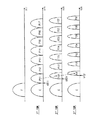
図1は、本発明に係る再プログラミング方式により実行されるメインプログラム動作を示す図である。図1は、3ビットデータ(または、LSBページのデータ、CSBページのデータ、MSBページのデータで構成される3ページのデータ)が再プログラム方式によってプログラムされる例を示す。しかし、再プログラム方式は3ビットデータに限定されない。再プログラム方式は、第1プログラム段階、第2プログラム段階、及び第3プログラム段階を含み、これは、以下詳細に説明する。
In a memory system that employs an on-chip buffer program method, the main program operation is performed using various programming methods. For example, the main program operation is performed based on a reprogram method. Hereinafter, the main program operation using the reprogramming method will be described in detail with reference to FIG.
FIG. 1 is a diagram illustrating a main program operation executed by the reprogramming method according to the present invention. FIG. 1 shows an example in which 3-bit data (or 3 page data composed of LSB page data, CSB page data, and MSB page data) is programmed by a reprogram method. However, the reprogramming method is not limited to 3-bit data. The reprogramming scheme includes a first program stage, a second program stage, and a third program stage, which will be described in detail below.
第1プログラム段階は、各メモリセルが8つの状態E、P11、P12、P13、P14、P15、P16、P17のうち3ビットのデータに対応する状態を有するように行われる。8つの状態E、P11〜P17は、図1に示すように、読み出しマージンなしに互いに隣接することができる。すなわち、第1プログラム段階では、3ビットのデータが概略的にプログラムされる。ここで、3ビットのデータは、バッファプログラム動作により、第1メモリ領域にプログラムされたデータであり、第1プログラム段階で、第1メモリ領域から読み出される。 The first program stage is performed such that each memory cell has a state corresponding to 3-bit data among the eight states E, P11, P12, P13, P14, P15, P16, and P17. As shown in FIG. 1, the eight states E, P11 to P17 can be adjacent to each other without a read margin. That is, in the first program stage, 3-bit data is roughly programmed. Here, the 3-bit data is data programmed in the first memory area by the buffer program operation, and is read from the first memory area in the first program stage.
例示的な実施形態において、第1プログラミング段階は、プログラムループの繰り返しの時にプログラム電圧が一定の増加分だけ増加する増加型ステップパルスプログラム(Incremental Step Pulse Programming:ISPP)技術に基づいて行われる。
例示的な実施形態において、第1プログラミング段階は検証動作を含む。検証動作の時、少なくとも一つのプログラム状態のみに対して検証動作を実行することができる。例えば、第1プログラミング段階で、プログラム状態P12、P14、P16の検証動作が実行される一方、プログラム状態P11、P13、P15、P17の検証動作は実行されない。つまり、プログラム状態P12、P14、P16が検証パスされれば、第1プログラミング段階は終了する。
In an exemplary embodiment, the first programming phase is performed based on Incremental Step Pulse Programming (ISPP) technology in which the program voltage is increased by a constant increment when the program loop is repeated.
In the exemplary embodiment, the first programming stage includes a verify operation. During the verification operation, the verification operation can be executed only for at least one program state. For example, in the first programming stage, the verification operation of the program states P12, P14, and P16 is executed, while the verification operation of the program states P11, P13, P15, and P17 is not executed. That is, if the program states P12, P14, and P16 are verified, the first programming stage is completed.
第2プログラミング段階は、第1プログラミング段階を通じて形成された概略的な状態(rough states)P11〜P17をより細密な状態P21〜P27に再プログラムするために行われる。ここで、状態P21〜P27は、図1に示すように、所定の読み出しマージンを有するように隣接することができる。つまり、第2プログラミング段階では、第1プログラミング段階でプログラムされた3ビットのデータが再プログラムされる。上述のように、第2プログラミング段階で使われる3ビットのデータは、第1プログラミング段階で使われたものと同様であり、第1メモリ領域から再び読み出される。図1に示すように、第1プログラミング段階の状態P11は、第2プログラミング段階の状態P21に再プログラムされる。これは、第2プログラミング段階の状態P21に対応する閾値電圧のばらつきが第1プログラミング段階の状態P11に対応する閾値電圧のばらつきより狭く形成されるようにする。すなわち、第2プログラミング段階の状態P21を検証するための検証電圧VR21は、第1プログラミング段階の状態P11を検証するための検証電圧VR11より高い。 The second programming phase is performed to reprogram the rough states P11 to P17 formed through the first programming phase to the finer states P21 to P27. Here, as shown in FIG. 1, the states P21 to P27 can be adjacent to each other with a predetermined read margin. That is, in the second programming stage, the 3-bit data programmed in the first programming stage is reprogrammed. As described above, the 3-bit data used in the second programming stage is the same as that used in the first programming stage, and is read again from the first memory area. As shown in FIG. 1, the state P11 of the first programming stage is reprogrammed to the state P21 of the second programming stage. This allows the threshold voltage variation corresponding to the second programming stage state P21 to be narrower than the threshold voltage variation corresponding to the first programming stage state P11. That is, the verification voltage VR21 for verifying the state P21 in the second programming stage is higher than the verification voltage VR11 for verifying the state P11 in the first programming stage.
例示的な実施形態において、第2プログラミング段階は、ISPP技術に基づいて行われる。
例示的な実施形態において、第2プログラミング段階は、検証動作を含む。検証動作はすべてのプログラム状態に対して行われる。すべてのプログラム状態P21〜P27が検証パスされれば、第2プログラミング段階は終了する。
In an exemplary embodiment, the second programming phase is performed based on ISPP technology.
In the exemplary embodiment, the second programming stage includes a verification operation. Verification operations are performed for all program states. If all the program states P21 to P27 are verified, the second programming phase ends.
第3プログラム段階は、第2プログラミング段階でプログラムされた状態P21〜P27をより細密な状態P31〜P37に再プログラムするために行われる。
ここで、状態P31〜P37は、図1に示すように、第2プログラミング段階の読み出しマージンより大きい読み出しマージンを有するように隣接することができる。すなわち、第3プログラム段階では、第2プログラミング段階でプログラムされた3ビットのデータが再プログラムされる。上述のように、第3プログラム段階で使われる3ビットのデータは、第1及び第2プログラミング段階で使われたものと同様であり、第1メモリ領域から再び読み出される。第3プログラミング段階が行われることによって、第2プログラミング段階の状態P21は、第3プログラム段階の状態P31に再プログラムされる。これは、第3プログラム段階の状態P31に対応する閾値電圧のばらつきが第2プログラミング段階の状態P21に対応する閾値電圧のばらつきより狭くする。すなわち、第3プログラム段階の状態31を検証するための検証電圧VR31が第2プログラミング段階の状態P21を検証するための検証電圧VR21より高い。
The third program stage is performed to reprogram the states P21 to P27 programmed in the second programming stage to the finer states P31 to P37.
Here, the states P31 to P37 may be adjacent to each other so as to have a read margin larger than the read margin in the second programming stage, as shown in FIG. That is, in the third program stage, the 3-bit data programmed in the second programming stage is reprogrammed. As described above, the 3-bit data used in the third program stage is the same as that used in the first and second programming stages, and is read again from the first memory area. By performing the third programming stage, the state P21 of the second programming stage is reprogrammed to the state P31 of the third programming stage. This makes the variation in threshold voltage corresponding to the state P31 in the third programming stage narrower than the variation in threshold voltage corresponding to the state P21 in the second programming stage. That is, the verification voltage VR31 for verifying the state 31 of the third program stage is higher than the verification voltage VR21 for verifying the state P21 of the second programming stage.
例示的な実施形態において、第3プログラム段階は、ISPP技術に基づいて行われる。
例示的な実施形態において、第3プログラム段階では、すべてのプログラム状態に対して検証動作が実行される。すべてのプログラム状態P31〜P37が検証パスされれば、第3プログラム段階は終了する。
In an exemplary embodiment, the third program phase is performed based on ISPP technology.
In the exemplary embodiment, in the third program phase, verification operations are performed for all program states. If all the program states P31 to P37 are verified, the third program phase ends.
本発明は、第1プログラミング段階で、3ビットのデータがプログラムされることに限定されない。本発明の第1プログラミング段階で、2ビットのデータがプログラムされることも可能である。2ビットのデータに対する第1プログラミング段階が完了した後、1ビットのデータをプログラムするために、第2プログラミング段階を行うことができる。その後、目標閾値電圧のばらつきを得るための第3プログラミング段階を行うことができる。上述のプログラムの方法は、特許文献1に掲載されている。
The present invention is not limited to
図1に示した3ビットプログラム動作が3ステップ再プログラミング方式によって実行される例を説明した。しかし、本発明は、3ビットプログラム動作が3ステップ再プログラミングによって実行されることに限定されない。本発明に係る再プログラミング方式により実行されるプログラム動作は、格納されるデータ値に対応する閾値電圧のばらつきの幅を狭くするため(または、閾値電圧のばらつきを正確に制御するため)の3つのプログラミング段階で構成することができる。 The example in which the 3-bit program operation shown in FIG. 1 is executed by the 3-step reprogramming method has been described. However, the present invention is not limited to performing 3-bit program operations by 3-step reprogramming. The program operation executed by the reprogramming method according to the present invention includes three operations for narrowing the threshold voltage variation corresponding to the stored data value (or for accurately controlling the threshold voltage variation). It can be configured in the programming stage.
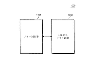
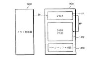
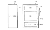
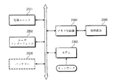
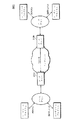
図2は、本発明の例示的な実施形態に係るメモリシステムを概略的に示すブロック図である。
図2を参照すると、本発明の実施形態に係るメモリシステム1000は、メモリ制御器1200と、マルチビットメモリ装置として不揮発性メモリ装置1400とを含む。メモリ制御器1200は、外部(例えば、ホスト)からの要請(例えば、書き込み要請、読み出し要請等)に応答して不揮発性メモリ装置1400を制御する。メモリ制御器1200は、外部からの要請なしに内部的な要請(例えば、サドンパワーオフ(Sudden Power Off)に係る動作、ウエアレベリング動作、読み出し校正(read reclaim)動作など)に応じて不揮発性メモリ装置1400を制御する。メモリ制御器1200の内部的な要請に対応する動作は、ホストからの要請が処理された後、ホストのタイムアウト区間内で行われる。または、メモリ制御器1200の内部的な要請に対応する動作は、メモリ制御器1200の遊休時間に行われる。不揮発性メモリ装置1400は、メモリ制御器1200の制御に応答して動作し、データの情報を格納する一種の格納媒体として使用される。格納媒体は、一つ以上のメモリチップで構成することができる。不揮発性メモリ装置1400とメモリ制御器1200は、一つ以上のチャネルを介して通信する。不揮発性メモリ装置1400は、例えば、NANDフラッシュメモリ装置を含む。
FIG. 2 is a block diagram schematically illustrating a memory system according to an exemplary embodiment of the present invention.
Referring to FIG. 2, a
メモリシステム1000は、上述のオンチップバッファプログラム(OBP)技術を使用する。以下で説明するように、不揮発性メモリ装置1400は、第1メモリ領域と第2メモリ領域とを有するメモリセルアレイを含む。例示的な実施形態において、第1メモリ領域は、セルあたり1ビットのデータを格納するメモリブロックで構成され、第2メモリ領域は、セル当たり3ビットのデータを格納するメモリブロックで構成される。第1メモリ領域及び第2メモリ領域の各々のセルあたりのビット数は、ここに開示されたものに限定されない。例えば、第1メモリ領域のセルあたりのビット数は、第2メモリ領域のセルあたりのビット数より少ない。メモリ制御器1200は、第2メモリ領域に含まれたメモリブロックのうちのいずれか一つのメモリブロックから読み出されたデータのエラービットの数が基準を超えたか否かに応じて読み出し校正動作(read reclaim operation)を実行する。本発明の読み出し校正動作によると、第2メモリ領域に含まれたメモリブロックに格納されたデータは、第2メモリ領域に含まれたメモリブロックに移動されるのではなく、第1メモリ領域に格納されたメモリブロックに移動する。本発明の場合、第2メモリ領域に含まれたメモリブロックに格納されたデータのすべてが第1メモリ領域に含まれたメモリブロックに移動すれば、第2メモリ領域に含まれたメモリブロックに係る読み出し校正動作は終了する。これは以後詳細に説明する。
The
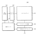
図3は、図2に示したメモリ制御器を概略的に示すブロック図である。図3を参照すると、メモリ制御器1200は、第1インターフェースとして、ホストインターフェース1210と、第2インターフェースとしてメモリインターフェース1220と、中央処理装置1230と、バッファメモリ1240と、ECC回路1250とを含む。
FIG. 3 is a block diagram schematically showing the memory controller shown in FIG. Referring to FIG. 3, the
ホストインターフェース1210は、外部(または、ホスト)とインターフェースするように構成される。メモリインターフェース1220は、図2に示した不揮発性メモリ装置1400とインターフェースするように構成される。CPU1230は、メモリ制御器1200の全体的な動作を制御するように構成される。例えば、CPU1230は、フラッシュ変換階層(Flash Translation Layer:FTL)のようなファームウェアを運用するように構成される。FTLは、様々な機能を実行する。例えば、FTLは、アドレスマッピング動作、読み出し校正動作、エラー訂正動作などを実行する様々な階層を含む。バッファメモリ1240は、ホストインターフェース1210を通じて外部に伝達されるデータを一時的に格納するために使用される。バッファメモリ1240は、メモリインターフェース1220を通じて不揮発性メモリ装置1400から伝達されるデータを一時的に格納するために使用される。バッファメモリ1240は、不揮発性メモリ装置1400を制御するために必要な情報(例えば、読み出し校正動作を必要とするソースメモリブロックを示す情報、アドレスマッピング情報など)を格納するために使用される。例えば、バッファメモリ1240は、DRAM、SRAM、またはDRAMとSRAMの組み合わせで構成することができる。しかし、バッファメモリ1240として使用されるメモリ装置は、ここに開示されたものに限定されない。ECC回路1250は、不揮発性メモリ装置1400に格納されるデータを符号化するように、そして不揮発性メモリ装置1400から読み出されたデータを復号化するように構成される。
The
例示的な実施形態において、メモリ制御器1200は、図示しないが、不揮発性メモリ装置1400に格納されるデータをランダム化するように、不揮発性メモリ装置1400から読み出されたデータをランダム化しないように構成されたランダマイザをさらに含む。ランダマイザの一例が特許文献2に掲載されている。
In the exemplary embodiment, the
例示的な実施形態において、ホストインターフェース1210は、コンピュータバス標準、ストレージバス標準、iFCPPeripheralバス標準などのうちの一つ以上の組み合わせで構成することができる。コンピュータバス標準(computer bus standards)は、S−100bus、Mbus、Smbus、Q−Bus、ISA、Zorro II、Zorro III、CAMAC、FASTBUS、LPC、EISA、VME、VXI、NuBus、TURBOchannel、MCA、Sbus、VLB、PCI、PXI、HP GSCbus、CoreConnect、InfiniBand、UPA、PCI−X、AGP、PCIe、Intel QuickPath Interconnect、Hyper Transportなどを含む。ストレージバス標準(Storage bus standards)は、ST−506、ESDI、SMD、Parallel ATA、DMA、SSA、HIPPI、USB MSC、FireWire(1394)、Serial ATA、eSATA、SCSI、Parallel SCSI、Serial Attached SCSI、Fibre Channel、iSCSI、SAS、RapidIO、FCIPなどを含む。iFCPPeripheralバス標準(iFCPPeripheral bus standards)は、Apple Desktop Bus、HIL、MIDI、Multibus、RS−232、DMX512−A、EIA/RS−422、IEEE−1284、UNI/O、1−Wire、I2C、SPI、EIA/RS−485、USB、Camera Link、External PCIe、Light Peak、Multidrop Busなどを含む。
In an exemplary embodiment, the
図4は、図2に示した不揮発性メモリ装置を概略的に示すブロック図である。
不揮発性メモリ装置1400は、例えば、NANDフラッシュメモリ装置である。しかし、本発明は、NANDフラッシュメモリ装置に限定されない。例えば、不揮発性メモリ装置1400は、NORフラッシュメモリ装置、RRAM(登録商標)(Resistive Random Access Memory)装置、PRAM(Phase−Change Memory)装置、MRAM(Magnetoresistive Random Access Memory)装置、FRAM(登録商標)(Ferroelectric Random Access Memory)装置、STT−RAM(Spin Transfer Torque Random Access Memory)などで構成することができる。また、本発明の不揮発性メモリ装置1400は、3次元アレイ構造を有するように実現することができる。3次元アレイ構造を有する不揮発性メモリ装置は、垂直NANDフラッシュメモリ装置と呼ばれる。本発明は、電荷格納層が伝導性の浮遊ゲートで構成されたフラッシュメモリ装置だけではなく、電荷格納層が絶縁膜で構成されるチャージトラップ型フラッシュ(Charge Trap Flash、“CTF”という)メモリ装置にも適用可能である。
FIG. 4 is a block diagram schematically showing the nonvolatile memory device shown in FIG.
The
図4を参照すると、不揮発性メモリ装置1400は、メモリセルアレイ1410と、アドレスデコーダ1420と、電圧発生器1430と、制御ロジック1440と、ページバッファ回路1450と、入出力インターフェース1460とを含む。
メモリセルアレイ1410は、行(例えば、ワードライン)と、列(例えば、ビットライン)との交差領域に配列されたメモリセルを含む。メモリセルの各々は、1ビットのデータまたはマルチビットのデータを格納する。アドレスデコーダ1420は、制御ロジック1440によって制御され、メモリセルアレイ1410の行(例えば、ワードライン、ストリング選択ライン、接地選択ライン、共通ソースラインなど)の選択及び駆動を行う。電圧発生器1430は、制御ロジック1440によって制御され、各動作に必要な電圧(例えば、高電圧、プログラム電圧、読み出し電圧、検証電圧、消去電圧、パス電圧、バルク電圧など)を発生する。電圧発生器1430によって生成された電圧は、アドレスデコーダ1420を通じてメモリセルアレイ1410に提供される。制御ロジック1440は、不揮発性メモリ装置1400の全体的な動作を制御するように構成される。
Referring to FIG. 4, the
The
ページバッファ回路1450は、制御ロジック1440によって制御され、メモリセルアレイ1410からデータを読み出すように、またはプログラムデータによってメモリセルアレイ1410の列(例えば、ビットライン)を駆動するように構成される。ページバッファ回路1450は、ビットライン又はビットライン対に各々対応する複数のページバッファで構成される。ページバッファの各々は、複数のラッチを含む。入出力インターフェース1460は、制御ロジック1440によって制御され、外部(例えば、図2のメモリ制御器1210)とインターフェースするように構成される。図示しないが、入出力インターフェース1460は、ページバッファを選択するための列選択器、データが入力される入力バッファ、データを出力する出力バッファなどを含む。
The
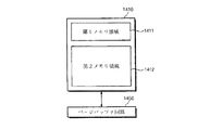
図5は、図4に示したメモリセルアレイを概略的に示すブロック図である。
図5を参照すると、メモリセルアレイ1410は、複数のメモリブロックで構成され、複数のメモリブロックは、第1メモリ領域1411と第2メモリ領域1412とに区分される。ここで、第1及び第2メモリ領域1411、1412の区分は物理的なものではなく、論理的に行われる。第1及び第2メモリ領域1411、1412の区分は、論理的に可変可能である。つまり、第1及び第2メモリ領域1411、1412の物理的なサイズがメモリ制御器1200の制御の下に論理的に可変可能である。第1メモリ領域1411に属するメモリブロックは、第2メモリ領域1412に属するメモリブロックとは異なる方法でプログラムされる。例えば、第1メモリ領域1411に属するメモリブロックは、単一ビットプログラム方法(または、SLCプログラム方式という)に基づいてプログラムされ、第2メモリ領域1412に属するメモリブロックは、マルチビットプログラム方法(または、MLC/TLCプログラム方式という)(例えば、上述の3ステップ再プログラム方式)に基づいてプログラムされる。つまり、第1メモリ領域1411に属するメモリセルの各々は、1ビットのデータを格納し、第2メモリ領域1412に属するメモリセルの各々は、Mビットデータ(Mは3以上の整数)を格納する。また、第1メモリ領域1411に属するメモリセルの各々は、第2メモリ領域1412に属するメモリセルの各々に格納されるデータビットの数より少ない数のデータビットを格納する。ここで、第1メモリ領域1411に属するメモリセルの各々が1ビットのデータを格納することに限定されない。例えば、第1メモリ領域1411に属するメモリセルの各々に格納されるビットの数は、第2メモリ領域1412に属するメモリセルの各々に格納されるビットの数より少ない。
FIG. 5 is a block diagram schematically showing the memory cell array shown in FIG.
Referring to FIG. 5, the
上述のように、メモリ制御器1200から提供されるデータは、バッファのプログラム動作を通じて、第1メモリ領域1411にプログラムされる。メインプログラム動作に必要なデータは、第1メモリ領域1411から読み出され、読み出されたデータは、メインプログラム動作を通じて第2メモリ領域1412にプログラムされる。
As described above, the data provided from the
図6A〜図6Dは、本発明の例示的な実施形態に係るマルチビットメモリ装置の第1及び第2メモリ領域に対する様々な組み合わせを説明するための図である。図面において、“BP”は、第1メモリ領域1411に対するバッファプログラミングを示し、“MP”は、第2メモリ領域1412に対するメインプログラミングを示す。
上述のように、マルチビットメモリ装置1400は、第1メモリ領域1411と第2メモリ領域1412とを含む。ここで、第1メモリ領域1411と第2メモリ領域1412は、マルチビットメモリ装置1400のメモリセルアレイを構成する。図示しないが、メモリセルアレイは、より多くの領域(例えば、メタ領域、予備領域など)を含む。メモリセルアレイのメモリ領域は物理的に区分されず、論理的に区分される。これは、メモリ制御器1200のアドレスマッピングに基づいて、メモリ領域が定義されることを意味する。
6A to 6D are diagrams illustrating various combinations of the first and second memory regions of the multi-bit memory device according to an exemplary embodiment of the present invention. In the drawing, “BP” indicates buffer programming for the
As described above, the
図6Aを参照すると、セル当たり3ビットのデータを格納するマルチビットメモリ装置の場合、第1メモリ領域1411は、1ビットのデータを各々格納するメモリセルのメモリブロックで構成し、第2メモリ領域1412は、3ビットのデータを各々格納するメモリセルのメモリブロックで構成することができる。この場合、バッファプログラミングは、SLCプログラム方式に基づいて行われる。メインプログラミングは、上述のMLC/TLCプログラム方法によって行われる。
Referring to FIG. 6A, in the case of a multi-bit memory device storing 3 bits of data per cell, the
図6Bを参照すると、セル当たり4ビットのデータを格納するマルチビットメモリ装置の場合、第1メモリ領域1411は、1ビットのデータを各々格納するメモリセルのメモリブロックで構成し、第2メモリ領域1412は、4ビットのデータを各々格納するメモリセルのメモリブロックで構成することができる。この場合、バッファプログラミングは、SLCプログラム方式に基づいて行われる。メインプログラミングは、上述のMLC/TLCプログラムの方法に基づいて行われる。
Referring to FIG. 6B, in the case of a multi-bit memory device storing 4 bits of data per cell, the
図6Cを参照すると、セル当たり3ビットのデータを格納するマルチビットメモリ装置の場合、第1メモリ領域1411は、2ビットのデータを各々格納するメモリセルのメモリブロックで構成し、第2メモリ領域1212は、3ビットのデータを各々格納するメモリセルのメモリブロックで構成することができる。この場合、バッファプログラミングは、一般的な、または、上述のMLCプログラム方式に基づいて行われる。メインプログラミングは、上述のMLC/TLCプログラム方法(例えば、再プログラム方式)に基づいて行われる。
Referring to FIG. 6C, in the case of a multi-bit memory device storing 3 bits of data per cell, the
図6Dを参照すると、セル当たり4ビットのデータを格納するマルチビットメモリ装置の場合、第1メモリ領域1411は、2ビットのデータを各々格納するメモリセルのメモリブロックで構成し、第2メモリ領域1412は、4ビットのデータを各々格納するメモリセルのメモリブロックで構成することができる。この場合、バッファのプログラミングは、一般的な、または、上述のMLCプログラム方式に基づいて行われる。メインプログラミングは、上述のMLC/TLCプログラム方法(例えば、再プログラム方式)に基づいて行われる。
Referring to FIG. 6D, in the case of a multi-bit memory device storing 4 bits of data per cell, the
例示的な実施例において、図6A〜図6Dに示した第1及び第2メモリ領域1411、1412の定義がここに開示されたものに限定されない。例えば、メモリシステムに含まれる格納媒体が複数のマルチビットメモリ装置で構成される場合、各マルチビットメモリ装置は、メモリセルアレイが第1及び第2メモリ領域1411、1412に区分されるように構成することができる。別の例として、1つまたはそれより多くのマルチビットメモリ装置のメモリセルアレイの各々は、第1メモリ領域1411として使用されるように構成することができる。残りのマルチビットメモリ装置のメモリセルアレイの各々は、第2メモリ領域1412として使用されるように構成することができる。
In the exemplary embodiment, the definitions of the first and
図7は、本発明の例示的な実施形態に係るメモリシステムの読み出し方法を示すフローチャートである。以下、本発明の例示的な実施形態に係るメモリシステムの読み出し方法を参照の図面に基づいて詳細に説明する。まず、第1メモリ領域1411は、セルあたり1ビットのデータが格納されるメモリブロック(以下、SLCブロックという)で構成され、第2メモリ領域1412は、セル当たり3ビットのデータが格納されるメモリブロック(以下、TLCブロックという)で構成されると仮定する。
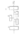
FIG. 7 is a flowchart illustrating a read method of a memory system according to an exemplary embodiment of the present invention. Hereinafter, a method for reading a memory system according to an exemplary embodiment of the present invention will be described in detail with reference to the accompanying drawings. First, the
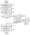
S110段階において、メモリ制御器1200は、外部装置(例えば、ホスト)からの読み出し要請が入力される。S120段階において、メモリ制御器1200は、読み出し要請されたデータが出力されるように不揮発性メモリ装置1400を制御する。読み出し要請されたデータは、例えば、第2メモリ領域1412のTLCブロックに格納されたデータである。または、読み出し要請されたデータは、第1メモリ領域1411のSLCブロックに格納されたデータである。例示的な実施形態において、読み出し要請されたデータは、第2メモリ領域1412のTLCブロックに格納されたデータである。
In step S110, the
S130段階において、不揮発性メモリ装置1400から出力されるデータがメモリ制御器1200のバッファメモリ1240に伝送される間、メモリ制御器1200のECC回路1250は、不揮発性メモリ装置1400から出力されるデータのエラー検出動作を実行する。この時、不揮発性メモリ装置1400から出力されるデータは、メモリ制御器1200のバッファメモリ1240に一時格納される。
In step S <b> 130, while the data output from the
S140段階において、不揮発性メモリ装置1400から出力されるデータのエラーが訂正可能であるか否か決められる。もし、不揮発性メモリ装置1400から出力されるデータのエラーが訂正可能であると判断されれば、S150段階に進行する。S150段階において、不揮発性メモリ装置1400から出力されるデータのエラーが訂正される。S160段階において、バッファメモリ1240に格納された訂正されたデータは、読み出し要請されたデータとして外部装置に伝送される。その後、読み出し方法は終了する。
In step S140, it is determined whether an error in data output from the
S140段階に戻って、もし不揮発性メモリ装置1400から出力されるデータのエラーが訂正できないと判断されれば、又は不揮発性メモリ装置1400から出力されるデータから出力されたエラービットの数が基準(例えば、ECC回路1250の許容可能なエラービット数)を超えた場合、S170段階に進む。S170段階において、メモリ制御器1200は、ソフトウェア方式で不揮発性メモリ装置1400から出力されるデータのエラー検出訂正動作を実行する。ソフトウェア方式を用いたエラー検出訂正動作は、例えば、FTLによって行われる。S180段階において、不揮発性メモリ装置1400から出力されるデータが訂正されたか否か決められる。たとえ不揮発性メモリ装置1400から出力されるデータに含まれるエラービットの数がECC回路1250の許容可能なエラービット数を超過しても、ソフトウェア方式を用いたエラー検出訂正動作を通じて不揮発性メモリ装置1400から出力されるデータのエラーを訂正することができる。
Returning to step S140, if it is determined that the error in the data output from the
不揮発性メモリ装置1400から出力されるデータが訂正されていないと判断されれば、S190段階に進む。S190段階において、メモリ制御器1200は、外部装置によって要請された読み出し動作をフェイルとして処理する。その後、読み出し方法は終了する。例えば、読み出しフェイルフラグが生成される。読み出しフェイルフラグの生成による手続きは多様に決定され得る。以後、方法は終了する。
If it is determined that the data output from the
不揮発性メモリ装置1400から出力されるデータが訂正されたと判断されれば、S200段階に進む。S200段階において、メモリ制御器1200は、バッファメモリ1240に格納された訂正されたデータを読み出し要請されたデータとして外部装置に伝送する。この時、読み出し要請されたデータが格納されたTLCブロックが読み出し校正動作を必要とするメモリブロックであることを示す情報がCPU1230の制御の下にキュー(queue)に格納される。以後、読み出し方法は終了する。
If it is determined that the data output from the
例示的な実施形態において、キューは、バッファメモリ1240の一部として構成され、キューに格納された情報は、CPU1230によって参照される。キューに格納された情報は、周期的に、または一定の時間に不揮発性メモリ装置1400に格納される。これは、突然の電源遮断によってバッファメモリ1240、またはキューに格納された情報が失われることを防止するために行われる。キューに格納された情報に基づいて、TLCブロックに対する読み出し校正動作が実行され、これは以後詳細に説明する。
In the exemplary embodiment, the queue is configured as part of
図8A及び図8Bは、本発明の例示的な実施形態に係る読み出し校正動作を示す図である。
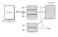
メモリセルの閾値電圧のばらつきは、様々な原因(例えば、温度変化、読み出し動作の繰り返し等)により移動することがある。閾値電圧のばらつきの移動は、メモリセルから読み出されたページのデータでエラービットが発生するようにする。例えば、閾値電圧のばらつきの移動は、エラービットの数を増加させる。特に、セル当たり3ビットのデータが格納されるTLCブロックの場合、閾値電圧のばらつきの移動は、エラービットの数をさらに増加させる。したがって、読み出されたデータの整合性を確保するために読み出し校正動作を実行することができる。読み出し校正動作は、訂正できないと判断されたページのデータを含んだTLCブロックの有効データを新しいブロックに移動させる動作を意味する。または、読み出し校正動作は、エラービットの数が今後増加する可能性が高いページのデータを含んだTLCブロックの有効データを新しいブロックに移動させる動作を意味する。読み出し校正動作は、ページのデータが格納されたメモリセルの閾値電圧のばらつきの移動が隣接したメモリセルにも影響を与えるため行われる。
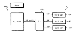
8A and 8B are diagrams illustrating a read calibration operation according to an exemplary embodiment of the present invention.
The variation in the threshold voltage of the memory cell may move due to various causes (for example, temperature change, repeated read operation, etc.). The shift of the threshold voltage variation causes an error bit to occur in the page data read from the memory cell. For example, shifting the threshold voltage variation increases the number of error bits. In particular, in the case of a TLC block in which 3 bits of data are stored per cell, the shift in the threshold voltage variation further increases the number of error bits. Therefore, a read calibration operation can be executed to ensure the consistency of the read data. The read calibration operation means an operation of moving valid data of a TLC block including data of a page determined to be uncorrectable to a new block. Alternatively, the read calibration operation means an operation of moving valid data of a TLC block including page data that is likely to increase in the number of error bits to a new block. The read calibration operation is performed because the shift of the threshold voltage variation of the memory cell storing the page data also affects the adjacent memory cell.
図8Aを参照すると、CPU1230は、キューに格納された情報に基づいて、FTLの読み出し校正動作の対象ブロックであるTLCブロックを選択する。例えば、選択されたTLCブロックは64個のワードラインを含むと仮定する。つまり、192個のページのデータが1つのTLCブロックに格納される。選択されたTLCブロックに格納された192個のページのデータが全部有効な場合、選択されたTLCブロックに格納された192個のページのデータを移動するための3つのSLCブロックが要求される。読み出し校正動作を実行するために選択されたTLCブロックから64個のページのデータが読み出され、読み出された64個のページのデータは、メモリ制御器1200のECC回路1250を通じて第1メモリ領域1411の一つのSLCブロックSB0に格納される。次に、読み出し校正動作を実行するために選択されたTLCブロックから64個のページのデータが読み出され、読み出された64個のページのデータは、メモリ制御器1200のECC回路1250を通じて第1メモリ領域1411のSLCブロックSB1に格納される。最後に、読み出し校正動作を実行するために選択されたTLCブロックから64個のページのデータが読み出され、読み出された64個のページのデータは、メモリ制御器1200のECC回路1250を通じて第1メモリ領域1411の一つのSLCブロックSB2に格納される。
Referring to FIG. 8A, the
図8Bを参照すると、選択されたTLCブロックに格納された192個のページのうち150個のページのデータが有効な場合、選択されたTLCブロックに格納された150個のページのデータを移動するための3つのSLCブロックが要求される。読み出し校正動作を実行するために選択されたTLCブロックから64個のページのデータが読み出され、読み出された64個のページのデータは、メモリ制御器1200のECC回路1250を通じて第1メモリ領域1411の一つのSLCブロックSB0に格納される。次に、読み出し校正動作を実行するために選択されたTLCブロックから64個のページのデータが読み出され、読み出された64個のページのデータは、メモリ制御器1200のECC回路1250を通じて第1メモリ領域1411のSLCブロックSB1に格納される。最後に、読み出し校正動作を実行するために選択されたTLCブロックから22個のページのデータが読み出され、読み出された22個のページのデータは、メモリ制御器1200のECC回路1250を通じて第1メモリ領域1411の一つのSLCブロックSB2に格納される。
TLCブロックに格納された有効なページのデータのすべてが、第1メモリ領域1411に移動すれば、CPU1230は、TLCブロックに対するFTLの読み出し校正動作を完了したと処理する。例えば、キューに格納された情報(読み出し校正動作の対象ブロック)が変更される。
Referring to FIG. 8B, when data of 150 pages out of 192 pages stored in the selected TLC block is valid, data of 150 pages stored in the selected TLC block is moved. Three SLC blocks for are required. 64 pages of data are read from the TLC block selected to execute the read calibration operation, and the 64 pages of read data are stored in the first memory area through the
If all the valid page data stored in the TLC block is moved to the
上述のように、本発明の読み出し校正動作によると、読み出し校正動作の対象ブロックであるTLCブロックの有効ページのデータは、第2メモリ領域1412のTLCブロックではなく、第1メモリ領域1411のSLCブロックに移動する。第1メモリ領域1411のSLCブロックへのデータの移動が完了すると、TLCブロックに対する読み出し校正動作が完了したと処理される。すなわち、本発明の読み出し校正動作の時、読み出し校正動作の対象ブロックであるTLCブロックの有効ページのデータは、第2メモリブロック1412のTLCブロックに移動しない。
As described above, according to the read calibration operation of the present invention, the valid page data of the TLC block that is the target block of the read calibration operation is not the TLC block of the
例示的な実施形態において、読み出し校正動作の対象ブロックであるTLCブロックの有効ページのデータは、時分割方式で、第1メモリ領域1411のSLCブロックに移動する。例えば、読み出し校正動作の対象ブロックであるTLCブロックの有効ページのデータの一部(例えば、一つのSLCブロックのサイズに対応する有効ページのデータ)が一つのSLCブロックに移動する。これは、他のページの読み出しまたは書き込み動作がホストによって要請されるたびに読み出しまたは書き込み動作が完了した後にタイムアウト時間内で行うことができる。TLCブロックの有効ページのデータのすべてがSLCブロックに移動する時、TLCブロックに対する読み出し校正動作は完了する。
In the exemplary embodiment, the valid page data of the TLC block that is the target block of the read calibration operation is moved to the SLC block in the
例示的な実施形態において、読み出し校正動作の対象ブロックであるTLCブロックの有効ページのデータが移動する第1メモリ領域1411のSLCブロックの数は、ホストのタイムアウト間隔を考慮して決めることができる。例えば、ホストの書き込み要請が処理された後、タイムアウト区間の残った時間を考慮して、第1メモリ領域1411のSLCブロックの数を決めることができる。ホストの書き込み要請の時、決められたSLCブロックに読み出し校正動作の対象ブロックであるTLCブロックのデータが移動する。
In the exemplary embodiment, the number of SLC blocks in the
TLCブロックからSLCブロックに移動したデータは、メインプログラム動作を通じて第2メモリ領域1412に格納される。これらの動作は、ガーベッジコレクション動作の間行うことができる。これは、図9を参照して詳細に説明する。
図9は、読み出し校正動作を通じて生成されたSLCブロックのデータがTLCブロックに格納される例を示す図である。
The data moved from the TLC block to the SLC block is stored in the
FIG. 9 is a diagram illustrating an example in which the data of the SLC block generated through the read calibration operation is stored in the TLC block.
上述のように、本発明の読み出し校正動作は、TLCブロックの有効ページのデータが第1メモリ領域1411のSLCブロックに移動する時に完了する。TLCブロックの有効ページの数に応じてSLCブロックのうちの一つは、空の格納空間を含む。例えば、図8B及び図9を参照すると、選択されたTLCブロックに格納された192個のページのうちで150個のページのデータが有効な場合、選択されたTLCブロックに格納された150個のページのデータを移動するために3つのSLCブロックが要求され、一つのSLCブロック(例えば、SB2)は空の格納空間を含む。空の格納空間を含むSLCブロックSB2を除いた残りのSLCブロックSB0、SB1のデータは、ガーベッジコレクションの動作の時にデータで完全に満たされた他のSLCブロック(例えば、SB3)のデータと共に特定のTLCブロックに格納される。SLCブロックのデータが上述のような方法でTLCブロックに格納されれば、TLCブロックは完全にデータで満たされる。すなわち、TLCブロックのすべてのワードラインがクローズされる。これは、TLCブロックがオープンワードラインを含まないことを意味する。一方、選択されたTLCブロックに格納された150個のページのデータが格納されたSLCブロックSB0、SB1、SB2のデータが特定のTLCブロックに格納される場合、特定のTLCブロックには、空の格納空間が存在する。これは、特定のTLCブロックがオープンワードラインを含むことを意味する。
As described above, the read calibration operation of the present invention is completed when the valid page data of the TLC block is moved to the SLC block of the
ここで、n番目のワードラインWLnに接続されたメモリセルに対する3ステップ再プログラム動作が完了した一方、隣接した上位ワードライン(例えば、n+1番目のワードラインWLn+1)に接続されたメモリセルに対する3ステップ再プログラム動作のうち、第3プログラミング段階が実行されない場合、n番目のワードラインWLnをオープンワードラインという。オープンワードラインに接続されたメモリセルの目標閾値電圧のばらつきは、隣接した上位ワードラインに接続されたメモリセルに対する3ステップ再プログラム動作が完了した時に形成される。もし、隣接した上位ワードラインに接続されたメモリセルに対する3ステップ再プログラム動作が完了しない場合、オープンワードラインに接続されたメモリセルの目標閾値電圧のばらつきが正常に形成されない。例えば、オープンワードラインに接続されたメモリセルは、隣接した上位ワードラインに接続されたメモリセルによって生じるカップリングを十分に受けず、その結果、オープンワードラインに接続されたメモリセルの目標閾値電圧のばらつきが正常に形成されない。このような場合、オープンワードラインに接続されたメモリセルから読み出されたデータは訂正不可能な確率が高くなる。 Here, the three-step reprogram operation for the memory cells connected to the nth word line WLn is completed, while the three steps for the memory cells connected to the adjacent upper word line (for example, the (n + 1) th word line WLn + 1). In the reprogram operation, when the third programming stage is not executed, the nth word line WLn is referred to as an open word line. The variation in the target threshold voltage of the memory cells connected to the open word line is formed when the three-step reprogram operation for the memory cells connected to the adjacent upper word line is completed. If the three-step reprogram operation for the memory cells connected to the adjacent upper word line is not completed, the variation of the target threshold voltage of the memory cells connected to the open word line is not normally formed. For example, a memory cell connected to an open word line does not sufficiently receive the coupling caused by a memory cell connected to an adjacent upper word line, resulting in a target threshold voltage of the memory cell connected to the open word line. The variation in size is not formed normally. In such a case, there is a high probability that the data read from the memory cell connected to the open word line cannot be corrected.
したがって、空の格納空間を含んだSLCブロックSB2を除いた残りのSLCブロックSB0、SB1のデータをガーベッジコレクション動作の時、データで完全に満たされた他のSLCブロック(例えば、SB3)のデータと共に、特定のTLCブロックに格納することによって、特定のTLCブロックでオープンワードラインが生じるのを防止することができる。
例示的な実施形態において、空の格納空間を有するSLCブロックSB2のデータは、空の格納空間を有する他のSLCブロックのデータと共に他のSLCブロックに、またはTLCブロックに移動することができる。
Therefore, the data of the remaining SLC blocks SB0 and SB1 excluding the SLC block SB2 including the empty storage space are combined with the data of other SLC blocks (for example, SB3) completely filled with the data at the time of the garbage collection operation. By storing in a specific TLC block, it is possible to prevent an open word line from occurring in the specific TLC block.
In an exemplary embodiment, the data of SLC block SB2 having an empty storage space can be moved to other SLC blocks or to a TLC block along with data of other SLC blocks having an empty storage space.
図10は、本発明の別の例示的な実施形態に係るメモリシステムの読み出し方法を示すフローチャートである。以下、本発明の例示的な実施形態に係るメモリシステムの読み出し方法を、参照の図面に基づいて詳細に説明する。まず、第1メモリ領域1411は、セルあたり1ビットのデータが格納されるメモリブロック(以下、SLCブロックという)で構成され、第2メモリ領域1412は、セル当たり3ビットのデータが格納されるメモリブロック(以下、TLCブロックという)で構成されると仮定する。
FIG. 10 is a flowchart illustrating a read method of a memory system according to another exemplary embodiment of the present invention. Hereinafter, a memory system read method according to an exemplary embodiment of the present invention will be described in detail with reference to the accompanying drawings. First, the
S310段階において、メモリ制御器1200は、外部装置(例えば、ホスト)からの読み出し要請が入力される。S320段階において、メモリ制御器1200は、読み出し要請されたデータが出力されるように不揮発性メモリ装置1400を制御する。読み出し要請されたデータは、例えば、第2メモリ領域1412のTLCブロックに格納されたデータである。または、読み出し要請されたデータは、第1メモリ領域1411のSLCブロックに格納されたデータである。例示的な実施形態において、読み出し要請されたデータは、第2メモリ領域1412のTLCブロックに格納されたデータである。
In step S310, the
S330段階において、不揮発性メモリ装置1400から出力されるデータが、メモリ制御器1200のバッファメモリ1240に伝送される間、メモリ制御器1200のECC回路1250は、不揮発性メモリ装置1400から出力されるデータに対するエラー検出動作を実行する。この時、不揮発性メモリ装置1400から出力されるデータは、メモリ制御器1200のバッファメモリ1240に一時格納される。
In step S330, while the data output from the
S340段階において、不揮発性メモリ装置1400から出力されるデータのエラーが訂正可能であるか否かが決められる。もし、不揮発性メモリ装置1400から出力されるデータのエラーが訂正可能であると判断されれば、S350段階に進む。S350段階において、不揮発性メモリ装置1400から出力されるデータのエラーが訂正される。S360段階において、バッファメモリ1240に格納された訂正されたデータは、読み出し要請されたデータとして外部装置に伝送される。その後、読み出し方法は終了する。
In step S340, it is determined whether an error in data output from the
S340段階に戻って、もし不揮発性メモリ装置1400から出力されるデータのエラーが訂正できないと判断されるか、又は不揮発性メモリ装置1400から出力されるデータから出力されたエラービットの数が基準(例えば、ECC回路1250の許容可能なエラービット数、許容可能なエラービット数より少ないエラービット数など)を超えた場合、S370段階に進む。S370段階において、読み出しリトライ動作が行われる。読み出しリトライ動作は、読み出し電圧が決められた回数内で変化する状態で読み出し動作をリトライする動作を意味する。読み出しリトライ動作の一例が特許文献3に掲載されている。読み出し電圧が変化するたびに読み出されたデータがエラー訂正可能であるか否かが判別される。読み出しリトライ動作を通じて読み出されたデータがエラー訂正できない場合、S380段階に進む。S380段階において、読み出しフェイルフラグが生成される。読み出しフェイルフラグの生成による手続きは多様に決定され得る。以後、方法は終了する。
Returning to step S340, if it is determined that the error of the data output from the
読み出しリトライ動作を通じて読み出されたデータがエラー訂正可能な場合、S390段階に進む。S390段階において、不揮発性メモリ装置1400から出力されたデータが格納された第2メモリ領域1412のTLCブロックが読み出し校正動作の対象ブロックであることを示す情報がキューに格納される。上述のように、キューは、バッファメモリ1240の一部として構成され、キューに格納された情報は、CPU1230によって参照される。キューに格納される情報は、周期的に、または一定の時間に不揮発性メモリ装置1400に格納される。これは、突然の電源遮断によってバッファメモリ1240、またはキューに格納された情報が失われることを防止するために行われる。キューに格納された情報に基づいて、TLCブロックの読み出し校正動作が実行され、これは以後詳細に説明する。
If the data read through the read retry operation can be corrected, the process proceeds to step S390. In step S390, information indicating that the TLC block in the
不揮発性メモリ装置1400から出力されたデータが格納された第2メモリ領域1412のTLCブロックが読み出し校正動作の対象ブロックであることを示す情報がキューに格納された後、S350段階に進む。S350段階において、不揮発性メモリ装置1400から出力されるデータのエラーが訂正される。S360段階において、バッファメモリ1240に格納された訂正されたデータは、読み出し要請されたデータとして外部装置に伝送される。以後、読み出し方法は終了する。
メモリ制御器1200は、キューに格納された情報に基づいて、読み出し校正動作を実行し、これは図8A、図8B、及び図9での説明と同様に行われる。
After the information indicating that the TLC block in the
The
図11は、本発明のさらに別の例示的な実施形態に係るメモリシステムの読み出し方法を示すフローチャートである。以下、本発明の例示的な実施形態に係るメモリシステムの読み出し方法を、参照の図面に基づいて詳細に説明する。まず、第1メモリ領域1411は、セルあたり1ビットのデータが格納されるメモリブロック(以下、SLCブロックという)で構成され、第2メモリ領域1412は、セル当たり3ビットのデータが格納されるメモリブロック(以下、TLCブロックという)で構成されると仮定する。
FIG. 11 is a flowchart illustrating a read method of a memory system according to still another exemplary embodiment of the present invention. Hereinafter, a memory system read method according to an exemplary embodiment of the present invention will be described in detail with reference to the accompanying drawings. First, the
S410段階において、メモリ制御器1200は、外部装置(例えば、ホスト)からの読み出し要請が入力される。S420段階において、メモリ制御器1200は、読み出し要請されたデータが出力されるように不揮発性メモリ装置1400を制御する。読み出し要請されたデータは、例えば、第2メモリ領域1412のTLCブロックに格納されたデータである。または、読み出し要請されたデータは、第1メモリ領域1411のSLCブロックに格納されたデータである。例示的な実施形態において、読み出し要請されたデータは、第2メモリ領域1412のTLCブロックに格納されたデータである。
In step S410, the
S430段階において、不揮発性メモリ装置1400から出力されるデータが、メモリ制御器1200のバッファメモリ1240に伝送される間、メモリ制御器1200のECC回路1250は、不揮発性メモリ装置1400から出力されるデータに対するエラー検出動作を実行する。この時、不揮発性メモリ装置1400から出力されるデータは、メモリ制御器1200のバッファメモリ1240に一時格納される。
In step S430, while the data output from the
S440段階において、不揮発性メモリ装置1400から出力されるデータに含まれたエラービットの数が基準以下であるか否かが決められる。ここで、基準は、ECC回路1250の許容可能なエラービット数、許容可能なエラービット数より少ないエラービット数などである。もし、不揮発性メモリ装置1400から出力されるデータに含まれたエラービットの数が基準以上であると判断されれば、S450段階に進む。S450段階において、不揮発性メモリ装置1400から出力されたデータが格納された第2メモリ領域1412のTLCブロックが読み出し校正動作の対象ブロックであることを示す情報がキューに格納される。上述のように、キューは、バッファメモリ1240の一部として構成され、キューに格納された情報は、CPU1230によって参照される。キューに格納される情報は、周期的に、または一定の時間に不揮発性メモリ装置1400に格納される。これは、突然の電源遮断によってバッファメモリ1240、またはキューに格納された情報が失われることを防止するために行われる。キューに格納された情報に基づいて、TLCブロックの読み出し校正動作が実行され、これは以後詳細に説明する。
In step S440, it is determined whether the number of error bits included in the data output from the
不揮発性メモリ装置1400から出力されたデータが格納された第2メモリ領域1412のTLCブロックが読み出し校正動作の対象ブロックであることを示す情報がキューに格納された後、S460段階に進む。S460段階において、不揮発性メモリ装置1400から出力されるデータのエラーが訂正される。S470段階において、バッファメモリ1240に格納された訂正されたデータは、読み出し要請されたデータとして外部装置に伝送される。以後、読み出し方法は終了する。
メモリ制御器1200は、キューに格納された情報に基づいて、読み出し校正動作を実行し、これは図8A、8b、及び図9での説明と同様に行われる。
After information indicating that the TLC block in the
The
図12は、本発明の例示的な実施形態に係るメモリシステムの読み出し校正方法を示すブロック図である。
図12を参照すると、読み出し校正動作は、読み出し動作の時、読み出しフェイルされる可能性が高いページのデータを含んだTLCブロックの有効なデータを新しいブロックに移動させる動作として、データの整合性を確保するために行われる。本発明では、特に、読み出し校正動作の対象ブロックとして決められたTLCブロックを示す情報がキューに格納される。ホストからの要請(例えば、書き込み要請)の時、例えば、要請された動作が完了し、キューに格納された情報に基づいてTLCブロックの有効なページのデータのうちの一部(または、すべて)がSLCブロックに移動する。SLCブロックへのデータ移動は、ECC回路1250の符号化及びバッファプログラミングを通じて行われる。
FIG. 12 is a block diagram illustrating a read calibration method of a memory system according to an exemplary embodiment of the present invention.
Referring to FIG. 12, in the read calibration operation, in the read operation, the data consistency of the TLC block including the data of the page that is highly likely to be read failed is moved to a new block. Done to ensure. In the present invention, in particular, information indicating the TLC block determined as the target block for the read calibration operation is stored in the queue. When requested by the host (for example, write request), for example, the requested operation is completed, and some (or all) of the valid page data of the TLC block based on the information stored in the queue Moves to the SLC block. Data movement to the SLC block is performed through encoding of the
例示的な実施形態において、ホスト要請の時、SLCブロックに移動するデータの量は、ホストのタイムアウト区間を考慮して決めることができる。例えば、SLCブロックに移動するデータの量は、一つのSLCブロックの格納容量に対応する。または、SLCブロックに移動するデータの量は、二つのSLCブロックの格納容量の合計に対応する。しかし、本発明は、ここに開示されたものに限定されない。したがって、要請された動作及びSLCブロックへのデータの移動は、ホストのタイムアウト区間内で行われる。 In the exemplary embodiment, when the host requests, the amount of data moved to the SLC block may be determined in consideration of the host timeout period. For example, the amount of data moved to the SLC block corresponds to the storage capacity of one SLC block. Alternatively, the amount of data moved to the SLC block corresponds to the total storage capacity of the two SLC blocks. However, the present invention is not limited to that disclosed herein. Therefore, the requested operation and data transfer to the SLC block are performed within the host timeout period.
読み出し校正動作の対象ブロックとして決められたTLCブロックの有効なページのデータがすべてSLCブロックに移動すれば、図12に示すように、TLCブロックと関連した読み出し校正動作は完了したと処理される。以後、SLCブロックに格納されたデータは、読み出し校正動作ではなく、ガーベッジコレクション動作または他の動作の時、メインプログラム動作によりTLCブロックに格納される。図9を参照して説明したように、読み出し校正動作を通じてプログラムされたSLCブロックのうちの一つが空の格納空間を含む場合、空の格納空間を含むSLCブロックを除いた残りのSLCブロックのデータは、他のSLCブロックのデータと共にメインプログラム動作によりTLCブロックに格納される。
したがって、本発明の読み出し校正動作は、ホストのタイムアウト条件を満たしながら実行することができる。また、本発明のメモリシステムは、TLCブロックにオープンワードラインが生成されることを防止することができる。
If all the valid page data of the TLC block determined as the target block for the read calibration operation is moved to the SLC block, the read calibration operation related to the TLC block is processed as shown in FIG. Thereafter, the data stored in the SLC block is stored in the TLC block by the main program operation during the garbage collection operation or other operations, not the read calibration operation. As described with reference to FIG. 9, when one of the SLC blocks programmed through the read calibration operation includes an empty storage space, data of the remaining SLC blocks excluding the SLC block including the empty storage space. Are stored in the TLC block by the main program operation together with the data of other SLC blocks.
Therefore, the read calibration operation of the present invention can be executed while satisfying the timeout condition of the host. In addition, the memory system of the present invention can prevent an open word line from being generated in the TLC block.
図13は、本発明の実施形態に係るコンピューティングシステムを概略的に示すブロック図である。コンピューティングシステムは、処理ユニット2101と、ユーザインターフェース2202と、ベースバンドチップセット(base band chipset)のようなモデム2303と、メモリ制御器2404と、格納媒体2505とを含む。
FIG. 13 is a block diagram schematically illustrating a computing system according to an embodiment of the present invention. The computing system includes a
メモリ制御器2404は、図2に示したものと実質的に同一に構成され、格納媒体2505は、図4に示した不揮発性メモリ装置で構成される。例えば、メモリ制御器2404は、読み出し校正動作の対象ブロックであるTLCブロックを、キューを利用して管理し、特定の時間(例えば、ホストの書き込み要請の時)に、キューに格納された情報に基づいてTLCブロックを選択し、選択されたTLCブロックの有効なページのデータが格納媒体2505の不揮発性メモリ装置に含まれたSLCブロックに移動するように格納媒体2505を制御する。メモリ制御器2404は、選択されたTLCブロックの有効なページのデータが格納媒体2505の不揮発性メモリ装置に含まれたSLCブロックに移動する時、選択されたTLCブロックの読み出し校正動作を完了したと処理する。
The
格納媒体2505には、処理ユニット2101によって処理された/処理されるNビットのデータ(Nは1以上の整数)がメモリ制御器2404を通じて格納される。コンピューティングシステムがモバイル装置の場合、コンピューティングシステムの動作電圧を供給するためのバッテリー2606がさらに提供される。図示しないが、本発明に係るコンピューティングシステムは、アプリケーションチップセット(application chipset)、カメライメージプロセッサ(Camera Image Processor:CIS)、モバイルDRAMなどをさらに提供することができる。
The
図14は、本発明の実施形態に係る半導体ドライブを概略的に示すブロック図である。
図14を参照すると、半導体ドライブ4000(SSD)は、格納媒体4100と、制御器4200とを含む。格納媒体4100は、複数のチャンネルCH0〜CHn1を通じて制御器4200と接続する。各チャンネルには、複数の不揮発性メモリが共通に接続するようになる。制御器4200は、図2に示したものと実質的に同一に構成され、格納媒体4100の不揮発性メモリ装置の各々は、図4に示した不揮発性メモリ装置と実質的に同一に構成される。例えば、制御器4200は、読み出し校正動作の対象ブロックであるTLCブロックを、キューを利用して管理し、特定の時間(例えば、ホストの書き込み要請の時)に、キューに格納された情報に基づいてTLCブロックを選択し、選択されたTLCブロックの有効なページのデータが格納媒体4100の不揮発性メモリ装置に含まれたSLCブロックに移動するように格納媒体4100を制御する。制御器4200は、選択されたTLCブロックの有効なページのデータが格納媒体4100の不揮発性メモリ装置に含まれたSLCブロックに移動する時、選択されたTLCブロックに対する読み出し校正動作を完了したと処理する。
FIG. 14 is a block diagram schematically showing a semiconductor drive according to the embodiment of the present invention.
Referring to FIG. 14, the semiconductor drive 4000 (SSD) includes a
図15は、図14に示した半導体ドライブを利用したストレージを概略的に示すブロック図であり、図16は、図14に示した半導体ドライブを利用したストレージサーバを概略的に示すブロック図である。
本発明の実施形態に係る半導体ドライブ4000は、ストレージを構成するために使用することができる。図15に示すように、ストレージは、図14での説明と実質的に同一に構成される複数の半導体ドライブを含む。本発明の実施形態に係る半導体ドライブ4000は、ストレージサーバを構成するために使用することができる。図16に示すように、ストレージサーバは、図14での説明と実質的に同一に構成される複数の半導体ドライブ4000と、サーバ4000Aとを含む。また、この分野でよく知られているRAID制御器4000Bをストレージサーバに提供することができることを容易に理解することができる。
FIG. 15 is a block diagram schematically showing storage using the semiconductor drive shown in FIG. 14, and FIG. 16 is a block diagram schematically showing a storage server using the semiconductor drive shown in FIG. .
The
図17は、本発明に係るMoviNANDを概略的に示すブロック図である。図17を参照すると、MoviNAND5000は、少なくとも一つのNANDフラッシュメモリ装置5100と、制御器5200とを含むことができる。MoviNAND5000は、MMC4.4(言い換えれば、eMMC)規格をサポートする。
FIG. 17 is a block diagram schematically showing a MoviNAND according to the present invention. Referring to FIG. 17, the
NANDフラッシュメモリ装置5100は、SDR(Sing Data Rate)NANDまたはDDR(Double Data Rate)NANDになることができる。例示的な実施形態において、NANDフラッシュメモリ装置5100は、単品のNANDフラッシュメモリ装置を含むことができる。ここで、単品のNANDフラッシュメモリ装置、一つのパッケージ(例えば、FBGA、Fine−pitch Ball Grid Array)に積層されて実現され得る。単品のNANDフラッシュメモリ装置の各々は、図4に示したものと実質的に同一に構成され、制御器5200は、図2に示したものと実質的に同一に動作する。例えば、メモリ制御器5200は、読み出し校正動作の対象ブロックであるTLCブロックをキューを用いて管理し、特定の時間(例えば、ホストの書き込み要請の時)に、キューに格納された情報に基づいてTLCブロックを選択し、選択されたTLCブロックの有効なページのデータがSLCブロックに移動するようにNANDフラッシュメモリ装置5100を制御する。メモリ制御器5200は、選択されたTLCブロックの有効なページのデータがNANDフラッシュメモリ装置5100に含まれたSLCブロックに移動する時、選択されたTLCブロックに対する読み出し校正動作を完了したと処理する。
The NAND
メモリ制御器5200は、複数のチャネルを通じてフラッシュメモリ装置5100に接続する。制御器5200は、少なくとも一つの制御器コア5210と、ホストインターフェース5220と、NANDインターフェース5230とを含む。少なくとも一つの制御器コア5210は、MoviNAND3000の全体的な動作を制御する。ホストインターフェース5220は、制御器5210とホストのインターフェイシングを実行する。NANDインターフェース5230は、NANDフラッシュメモリ装置5100と制御器5200のインターフェイシングを実行する。例示的な実施形態において、ホストインターフェース5220は、並列インターフェース(例えば、MMCインターフェース)になることができる。別の実施形態において、MoviNAND5000のホストインターフェース5220は、直列インターフェース(例えば、UHS−II、UFSインターフェース)になることができる。
The
MoviNAND5000は、ホストから電源電圧Vcc、Vccqが提供される。ここで、第1電源電圧(Vcc:3.3V)は、NANDフラッシュメモリ装置5100とNANDインターフェース5230に提供され、第2電源電圧(Vccq:1.8V/3.3V)は、制御器5200に提供される。例示的な実施形態において、MoviNAND5000は、外部の高電圧Vppが選択的に提供され得る。
本発明に係るMoviNAND5000は、大容量のデータの格納に有利であるだけでなく、向上した読み出し動作特性を有する。本発明の実施形態に係るMoviNAND5000は、小型及び低電力が要求されるモバイル製品(例えば、GALAXY S、GALAXY Note、iPhoneなど)に応用可能である。
The
The
図18は、本発明に係る通信装置を概略的に示すブロック図である。図18を参照すると、モバイル装置6000は、通信ユニット6100と、制御器6200と、メモリユニット6300と、ディスプレイユニット6400と、タッチスクリーンユニット6500と、オーディオユニット6600とを含む。メモリユニット6300は、少なくとも一つのDRAM6310と、少なくとも一つのOneNAND6320と、少なくとも一つのMoviNAND6330とを含む。
モバイル装置に関するより詳細な説明は、特許文献4、5、6、7及び8に記載されている。
FIG. 18 is a block diagram schematically showing a communication apparatus according to the present invention. Referring to FIG. 18, the
More detailed descriptions regarding mobile devices are described in US Pat.
図19は、本発明の実施形態に係る半導体ドライブが適用されるシステムを概略的に示す図である。
図19に示すように、本発明の実施形態に係る半導体ドライブは、メールサーバ8100にも適用可能である。
FIG. 19 is a diagram schematically showing a system to which the semiconductor drive according to the embodiment of the present invention is applied.
As shown in FIG. 19, the semiconductor drive according to the embodiment of the present invention can also be applied to the
図20は、本発明の実施形態に係るメモリカード(memory card)を概略的に示すブロック図である。
メモリカードは、例えば、MMCカード、SDカード、マルチユース(multiuse)カード、マイクロSDカード、メモリスティック、コンパクトSDカード、IDカード、PCMCIAカード、SSDカード、チップカード(chipcard)、スマートカード(smartcard)、USBカードなどになることができる。
FIG. 20 is a block diagram schematically showing a memory card according to an embodiment of the present invention.
The memory card is, for example, an MMC card, an SD card, a multi-use card, a micro SD card, a memory stick, a compact SD card, an ID card, a PCMCIA card, an SSD card, a chip card (chipcard), a smart card (smart card). It can be a USB card or the like.
図20を参照すると、メモリカードは、外部とのインターフェースを実行するインターフェース部9221と、バッファメモリを有し、メモリカードの動作を制御する制御器9222と、1つ以上の不揮発性メモリ装置9207とを含む。
制御器9222は、プロセッサとして、不揮発性メモリ装置9207のライト動作及びリード動作を制御することができる。具体的に、制御器9222は、データバスDATAとアドレスバスADDRESSとを通じて不揮発性メモリ装置9207及びインターフェース部9221とカップリングされている。インターフェース部9221は、ホストとメモリカードとの間のデータ交換を実行するためのカードプロトコル(例えば、SD/MMC)を通じてホストとインターフェイシングする。
Referring to FIG. 20, the memory card includes an
The
制御器9222は、図2に示したものと実質的に同一に構成され、不揮発性メモリ装置9207は、図4に示した不揮発性メモリ装置と実質的に同一に構成される。例えば、制御器9222は、読み出し校正動作の対象ブロックであるTLCブロックを、キューを利用して管理し、特定の時間(例えば、ホストの書き込み要請の時)に、キューに格納された情報に基づいてTLCブロックを選択し、選択されたTLCブロックの有効なページのデータが不揮発性メモリ装置9207に含まれたSLCブロックに移動するように不揮発性メモリ装置9207を制御する。制御器9222は、選択されたTLCブロックの有効なページのデータが不揮発性メモリ装置9207に含まれたSLCブロックに移動する時、選択されたTLCブロックに対する読み出し校正動作を完了したと処理する。
The
図21は、本発明の実施形態に係るデジタルスチルカメラ(digital still camera)を概略的に示すブロック図である。
図21を参照すると、デジタルスチルカメラは、ボディ9301と、スロット9302と、レンズ9303と、ディスプレイ部9308と、シャッターボタン9312と、ストローブ(strobe)9318などを含む。特に、スロット9308には、メモリカード9331を挿入することができ、メモリカード9331は、図1で説明したメモリ制御器と不揮発性メモリ装置とを含む。例えば、メモリ制御器は、読み出し校正動作の対象ブロックであるTLCブロックを、キューを利用して管理し、特定の時間(例えば、ホストの書き込み要請の時)に、キューに格納された情報に基づいてTLCブロックを選択し、選択されたTLCブロックの有効なページのデータが不揮発性メモリ装置に含まれたSLCブロックに移動するように不揮発性メモリ装置を制御する。メモリ制御器は、選択されたTLCブロックの有効なページのデータが不揮発性メモリ装置に含まれたSLCブロックに移動する時、選択されたTLCブロックに対する読み出し校正動作を完了したと処理する。
FIG. 21 is a block diagram schematically showing a digital still camera according to an embodiment of the present invention.
Referring to FIG. 21, the digital still camera includes a
メモリカード9331が接触型(contact type)の場合、メモリカード9331がスロット9308に挿入される時、メモリカード9331と回路基板上の特定の電気回路が電気的に接触することになる。メモリカード9331が、非接触型(noncontact type)の場合、無線信号を通じてメモリカード9331がアクセスされる。
When the
図22は、図21のメモリカードが使用される様々な応用分野を示す図である。
図22を参照すると、メモリカード9331は、ビデオカメラ(VC)、テレビ(TV)、オーディオ装置(AD)、ゲーム装置(GM)、電子音楽装置(EMD)、携帯電話(HP)、コンピュータ(CP)、PDA(Personal Digital Assistant)、ボイスレコーダ(voice recorder)(VR)、PCカード(PCC)などに使用することができる。
本発明の実施形態において、メモリセルは、可変抵抗メモリセルで構成することができ、例示的な可変抵抗メモリセル及びそれを含むメモリ装置は、特許文献9に掲載されている。
FIG. 22 is a diagram showing various application fields in which the memory card of FIG. 21 is used.
Referring to FIG. 22, the
In the embodiment of the present invention, the memory cell can be composed of a variable resistance memory cell, and an exemplary variable resistance memory cell and a memory device including the variable resistance memory cell are disclosed in Patent Document 9.
本発明の別の実施形態において、メモリセルは、電荷格納層を有する多様なセル構造のうちの一つを使用して実現することができる。電荷格納層を有するセル構造は、電荷トラップ層を利用する電荷トラップフラッシュ構造、アレイが多層で積層されるスタックフラッシュ構造、ソース/ドレインがないフラッシュ構造、ピンタイプフラッシュ構造などを含む。
電荷格納層として電荷トラップフラッシュ構造を有するメモリ装置が、特許文献10、11、12に各々掲載されている。ソース/ドレインがないフラッシュ構造は、特許文献13に掲載されている。
In another embodiment of the present invention, the memory cell can be implemented using one of a variety of cell structures having a charge storage layer. Cell structures having a charge storage layer include a charge trap flash structure using a charge trap layer, a stack flash structure in which arrays are stacked in multiple layers, a flash structure without source / drain, a pin type flash structure, and the like.
Memory devices having a charge trap flash structure as a charge storage layer are disclosed in Patent Documents 10, 11, and 12, respectively. A flash structure having no source / drain is disclosed in Patent Document 13.
本発明に係るフラッシュメモリ装置及び/またはメモリ制御器は、多様な形態のパッケージを利用して実装することができる。例えば、本発明に係るフラッシュメモリ装置及び/またはメモリ制御器は、PoP(Package on Package)、Ball grid arrays(BGAs)、Chip scale packages(CSPs)、Plastic Leaded Chip Carrier(PLCC)、Plastic Dual In−Line Package(PDIP)、Die in Waffle Pack、Die in Wafer Form、Chip On Board(COB)、Ceramic Dual In−Line Package(CERDIP)、Plastic Metric Quad Flat Pack(MQFP)、Thin Quad Flatpack(TQFP)、Small Outline(SOIC)、Shrink Small Outline Package(SSOP)、Thin Small Outline(TSOP)、Thin Quad Flatpack(TQFP)、System In Package(SIP)、Multi Chip Package(MCP)、Wafer−level Fabricated Package(WFP)、Wafer−Level Processed Stack Package(WSP)などのようなパッケージを利用して実装することができる。 The flash memory device and / or the memory controller according to the present invention can be mounted using various types of packages. For example, the flash memory device and / or the memory controller according to the present invention includes PoP (Package on Package), Ball grid arrays (BGAs), Chip scale packages (CSPs), Plastic Leaded Chip Carrier (PLCC), Plastic In D Line Package (PDIP), Die in Waffle Pack, Die in Wafer Form, Chip On Board (COB), Ceramic Dual In-Line Package (CERDIP), Plastic Metal Tack Outline SOIC), Shrink Small Outline Package (SSOP), Thin Small Outline (TSOP), Thin Quad Flatpack (TQFP), System In Package (FIP), MultiChip Package (MCP), Multi Chip Package (MCP). It can be implemented using a package such as Level Processed Stack Package (WSP).
本発明の範囲又は技術的思想を逸脱せずに本発明の構造を多様に修正又は変更可能であることはこの分野に熟練している者に自明である。上述の内容を考慮する時、本発明の修正及び変更が添付の特許請求の範囲及びその均等物の範疇内に属すれば、本発明はこの発明の変更及び修正を含むと見なす。 It will be apparent to those skilled in the art that various modifications and variations can be made to the structure of the present invention without departing from the scope or spirit of the invention. In light of the foregoing, the present invention is deemed to include modifications and variations of this invention provided that such modifications and changes fall within the scope of the appended claims and their equivalents.
1000 メモリシステム
1200 メモリ制御器
1210 ホストインターフェース
1220 メモリインターフェース
1230 CPU
1240 バッファメモリ
1250 ECC回路
1400 不揮発性メモリ装置
1410 メモリセルアレイ
1411 第1メモリ領域
1412 第2メモリ領域
1420 アドレスデコーダ
1430 電圧発生器
1440 制御ロジック
1450 ページバッファ回路
1460 入出力インターフェース
1000
1240
Claims (30)
読出し動作、プログラム動作、及び再プログラム動作を遂行するために前記不揮発性メモリ装置を制御する制御器と、を含み、 A controller for controlling the non-volatile memory device to perform a read operation, a program operation, and a reprogram operation,
前記制御器は、エラー訂正された(ECC(error checking and correction)−performed)第1データを生成するために前記第1データに対するECC動作を遂行するように構成され、 The controller is configured to perform an ECC operation on the first data in order to generate error-corrected (ECC (error checking and correction) -performed) first data;
前記第1データは、第1電圧レベルで前記複数の第1メモリセルの第1部分から読み出され、 The first data is read from a first portion of the plurality of first memory cells at a first voltage level;
前記エラー訂正された第1データのエラービットの数が前記ECC動作によって修正可能な閾値(threshold)を超過する時、前記制御器は、エラー訂正された第2データを生成するために第2データに対するリードリトライ(read retry)動作及びECC動作を遂行するように構成され、 When the number of error bits of the error-corrected first data exceeds a threshold that can be corrected by the ECC operation, the controller generates second data to generate error-corrected second data. Configured to perform a read retry operation and an ECC operation for
前記リードリトライ動作は、第2電圧レベルで前記複数の第1メモリセルの前記第1部分に格納された前記第2データを読み出すことを含み、 The read retry operation includes reading the second data stored in the first portion of the plurality of first memory cells at a second voltage level;
ここで、前記第2電圧レベルは、前記第1電圧レベルと異なり、 Here, the second voltage level is different from the first voltage level,
前記第2データは、前記複数の第1メモリセルの前記第1部分から読み出され、 The second data is read from the first portion of the plurality of first memory cells;
前記制御器は、前記エラー訂正された第1データ及び前記エラー訂正された第2データのうちのいずれか1つを有する第1ページデータを前記不揮発性メモリ装置に出力するように構成され、 The controller is configured to output first page data having one of the error-corrected first data and the error-corrected second data to the nonvolatile memory device;
前記不揮発性メモリ装置は、前記複数の第2メモリセルの第1部分に前記第1ページデータをプログラムするように構成され、 The non-volatile memory device is configured to program the first page data in a first portion of the plurality of second memory cells,
前記不揮発性メモリ装置は、前記複数の第2メモリセルの前記第1部分で前記プログラムされた第1ページデータを読み出すように構成され、 The non-volatile memory device is configured to read the programmed first page data in the first portion of the plurality of second memory cells,
前記不揮発性メモリ装置は、前記複数の第2メモリセルの前記第1部分から第1時間に読み出された前記プログラムされた第1ページデータを前記複数の第1メモリセルの第2部分にプログラムするように構成され、 The non-volatile memory device programs the programmed first page data read from the first portion of the plurality of second memory cells at a first time into the second portion of the plurality of first memory cells. Configured to
前記不揮発性メモリ装置は、前記複数の第2メモリセルの前記第1部分から第2時間に読み出された前記プログラムされた第1ページデータを前記複数の第1メモリセルの前記第2部分に再プログラムするように構成されるメモリシステム。 The nonvolatile memory device may store the programmed first page data read from the first portion of the plurality of second memory cells at a second time in the second portion of the plurality of first memory cells. A memory system configured to reprogram.
前記第2ページデータは、前記制御器から前記不揮発性メモリ装置に出力される請求項5に記載のメモリシステム。 The memory system according to claim 5, wherein the second page data is output from the controller to the nonvolatile memory device.
複数の第2メモリブロックに形成され、セル当たり3ビットデータを格納するように構成されたフラッシュメモリセルの第2グループと、 A second group of flash memory cells formed in a plurality of second memory blocks and configured to store 3-bit data per cell;
を含む不揮発性メモリ装置と、 A non-volatile memory device comprising:
前記不揮発性メモリ装置を制御するように構成されたメモリ制御器と、を含み、 A memory controller configured to control the non-volatile memory device;
前記メモリ制御器は、前記複数の第2メモリブロックのうちのいずれか1つに格納された有効なデータを前記複数の第1メモリブロックのうちの1つ以上のメモリブロックに伝送するためのリードリクレイム(read reclaim)動作を遂行するように構成され、 The memory controller is configured to read valid data stored in any one of the plurality of second memory blocks to one or more memory blocks of the plurality of first memory blocks. Configured to perform a read reclaim operation;
前記リードリクレイム動作は、第1時間に前記有効なデータの第1部分に対して遂行され、前記第1時間と異なる第2時間に前記有効なデータの第2部分に対して遂行され、 The read reclaim operation is performed on the first portion of the valid data at a first time, and is performed on the second portion of the valid data at a second time different from the first time;
前記メモリ制御器は、前記複数の第1メモリブロックのうちの前記1つ以上のメモリブロックから読み出された前記有効なデータの第3部分を前記複数の第2メモリブロックの前記いずれか1つと異なる前記複数の第2メモリブロックのうちのいずれか1つに伝送するように1つ以上のプログラム動作を遂行するように構成されるメモリシステム。 The memory controller may convert a third portion of the valid data read from the one or more memory blocks of the plurality of first memory blocks to any one of the plurality of second memory blocks. A memory system configured to perform one or more program operations to be transmitted to any one of the different second memory blocks.
前記第2プログラム段階に対応する第2閾値電圧幅は、前記第1プログラム段階に対応する第1閾値電圧幅より狭い請求項14に記載のメモリシステム。 The memory system of claim 14, wherein the second threshold voltage width corresponding to the second program stage is narrower than the first threshold voltage width corresponding to the first program stage.
前記第1時間周期及び前記第2時間周期は、互いに分離される請求項16に記載のメモリシステム。 The memory system of claim 16, wherein the first time period and the second time period are separated from each other.
第1電圧レベルで、前記複数の第1メモリセルの第1部分から第1データを読み出す段階と、 Reading first data from a first portion of the plurality of first memory cells at a first voltage level;
エラー訂正された第1データを生成するために前記第1データに対するECC(error checking and corretion)動作を遂行する段階と、 Performing an error checking and correction (ECC) operation on the first data to generate error-corrected first data;
前記エラー訂正された第1データのエラービットの個数が前記ECC動作によって訂正可能な閾値を超過する時、第2電圧レベルで、前記複数の第1メモリセルの前記第1部分から第2データを読み出す段階と、 When the number of error bits of the error-corrected first data exceeds a threshold that can be corrected by the ECC operation, the second data from the first portion of the plurality of first memory cells is applied at a second voltage level. Reading out,
エラー訂正された第2データを生成するために前記第2データに対するECC動作を遂行する段階と、 Performing an ECC operation on the second data to generate error-corrected second data;
前記エラー訂正された第1データ及び前記エラー訂正された第2データのうちのいずれか1つを有する第1ページデータを前記不揮発性メモリ装置に出力する段階と、 Outputting first page data having one of the error-corrected first data and the error-corrected second data to the nonvolatile memory device;
前記複数の第2メモリセルの第1部分に前記第1ページデータをプログラムする段階と、 Programming the first page data in a first portion of the plurality of second memory cells;
第1時間に前記複数の第2メモリセルの前記第1部分から前記プログラムされたページデータを読み出す段階と、 Reading the programmed page data from the first portion of the plurality of second memory cells at a first time;
前記第1時間に読み出された前記プログラムされた第1ページデータを前記複数の第1メモリセルの第2部分にプログラムする段階と、 Programming the programmed first page data read at the first time into a second portion of the plurality of first memory cells;
第2時間に前記複数の第2メモリセルの前記第1部分から前記プログラムされた第1ページデータを読み出す段階と、 Reading the programmed first page data from the first portion of the plurality of second memory cells at a second time;
前記第2時間に読み出された前記プログラムされた第1ページデータを前記複数の第1メモリセルの前記第2部分に再プログラムする段階と、を含む方法。 Reprogramming the programmed first page data read at the second time into the second portion of the plurality of first memory cells.
前記第3データは、第2ページデータに含まれ、 The third data is included in the second page data,
前記第2ページデータは、前記制御器から前記不揮発性メモリ装置に出力され、 The second page data is output from the controller to the nonvolatile memory device,
前記第1ページデータ及び前記第2ページデータは、事前に決定された時間周期内に前記制御器から前記不揮発性メモリ装置に出力される請求項19に記載の方法。 The method of claim 19, wherein the first page data and the second page data are output from the controller to the non-volatile memory device within a predetermined time period.
読出し動作、プログラム動作、及び再プログラム動作を遂行するために前記不揮発性メモリ装置を制御する制御器と、を含み、 A controller for controlling the non-volatile memory device to perform a read operation, a program operation, and a reprogram operation,
前記制御器は、エラー訂正された第1データを生成するために前記第1データに対するECC動作を遂行するように構成され、 The controller is configured to perform an ECC operation on the first data to generate error-corrected first data;
前記第1データは、第1電圧レベルで前記複数の第1メモリセルの第1部分から読み出され、 The first data is read from a first portion of the plurality of first memory cells at a first voltage level;
前記エラー訂正された第1データのエラービットの個数が前記ECC動作によって訂正可能な閾値を超過する時、前記制御器は、エラー訂正された第2データを生成するためにリードリトライ動作及びECC動作を遂行するように構成され、 When the number of error bits of the error-corrected first data exceeds a threshold that can be corrected by the ECC operation, the controller performs a read retry operation and an ECC operation to generate error-corrected second data. Configured to carry out
前記リードリトライ動作は、前記第1電圧レベルと異なる第2電圧レベルで前記複数の第1メモリセルの前記第1部分に格納された第2データを読み出すことを含み、 The read retry operation includes reading second data stored in the first portion of the plurality of first memory cells at a second voltage level different from the first voltage level;
前記第2データは、前記複数の第1メモリセルの前記第1部分から読み出され、 The second data is read from the first portion of the plurality of first memory cells;
前記制御器は、前記エラー訂正された第1データ及び前記エラー訂正された第2データのうちのいずれか1つを含む第1ページデータを前記不揮発性メモリ装置に出力するように構成され、 The controller is configured to output first page data including any one of the error-corrected first data and the error-corrected second data to the nonvolatile memory device;
前記不揮発性メモリ装置は、前記複数の第2メモリセルの第1部分に前記第1ページデータをプログラムするように構成され、 The non-volatile memory device is configured to program the first page data in a first portion of the plurality of second memory cells,
前記不揮発性メモリ装置は、前記複数の第2メモリセルの前記第1部分から前記プログラムされた第1ページデータを読み出すように構成され、 The nonvolatile memory device is configured to read the programmed first page data from the first portion of the plurality of second memory cells,
前記不揮発性メモリ装置は、第1時間で前記複数の第2メモリセルの前記第1部分から読み出された前記プログラムされた第1ページデータを前記複数の第1メモリセルの第2部分にプログラムするように構成され、 The non-volatile memory device programs the programmed first page data read from the first portion of the plurality of second memory cells in a first time into the second portion of the plurality of first memory cells. Configured to
前記不揮発性メモリ装置は、第2時間で前記複数の第2メモリセルの前記第1部分から読み出された前記プログラムされた第1ページデータを前記複数の第1メモリセルの前記第2部分に再プログラムするように構成され、 The non-volatile memory device stores the programmed first page data read from the first portion of the plurality of second memory cells in the second portion of the plurality of first memory cells in a second time. Configured to reprogram,
前記第1時間は、前記第2時間と異なるメモリシステム。 The first time is a memory system different from the second time.
前記第2ページデータは、前記制御器から前記不揮発性メモリ装置に出力される請求項27に記載のメモリシステム。 28. The memory system of claim 27, wherein the second page data is output from the controller to the nonvolatile memory device.
Applications Claiming Priority (2)
| Application Number | Priority Date | Filing Date | Title |
|---|---|---|---|
| KR1020120110859A KR102025263B1 (en) | 2012-10-05 | 2012-10-05 | Memory system and read reclaim method thereof |
| KR10-2012-0110859 | 2012-10-05 |
Publications (3)
| Publication Number | Publication Date |
|---|---|
| JP2014078229A JP2014078229A (en) | 2014-05-01 |
| JP2014078229A5 JP2014078229A5 (en) | 2016-12-08 |
| JP6202972B2 true JP6202972B2 (en) | 2017-09-27 |
Family
ID=50407749
Family Applications (1)
| Application Number | Title | Priority Date | Filing Date |
|---|---|---|---|
| JP2013210121A Active JP6202972B2 (en) | 2012-10-05 | 2013-10-07 | Memory system and reading calibration method thereof |
Country Status (4)
| Country | Link |
|---|---|
| US (3) | US9431117B2 (en) |
| JP (1) | JP6202972B2 (en) |
| KR (1) | KR102025263B1 (en) |
| CN (1) | CN103714856B (en) |
Families Citing this family (84)
| Publication number | Priority date | Publication date | Assignee | Title |
|---|---|---|---|---|
| KR102025263B1 (en) * | 2012-10-05 | 2019-09-25 | 삼성전자주식회사 | Memory system and read reclaim method thereof |
| TWI533305B (en) * | 2014-02-10 | 2016-05-11 | 慧榮科技股份有限公司 | Method for writing data into flash memory and associated memory device and flash memory |
| US8886877B1 (en) * | 2014-05-15 | 2014-11-11 | Sandisk Technologies Inc. | In-situ block folding for nonvolatile memory |
| CN105224241A (en) * | 2014-06-23 | 2016-01-06 | 联想(北京)有限公司 | Mram memory, data-storage system and method for reading data |
| KR20160016421A (en) * | 2014-08-05 | 2016-02-15 | 삼성전자주식회사 | Method of optimizing non-volatile memory based storage device |
| US9529668B2 (en) * | 2014-09-26 | 2016-12-27 | Intel Corporation | Method and system for using NAND page buffers to improve the transfer buffer utilization of a solid state drive |
| KR102238652B1 (en) | 2014-11-12 | 2021-04-09 | 삼성전자주식회사 | Data storage devce, method thereof, and method for operating data processing system having the same |
| TWI559314B (en) * | 2014-12-27 | 2016-11-21 | 群聯電子股份有限公司 | Memory management method, memory storage device and memory controlling circuit unit |
| KR102277521B1 (en) | 2015-01-23 | 2021-07-16 | 삼성전자주식회사 | Storage device and read reclaim and reading method thereof |
| KR102403253B1 (en) | 2015-07-06 | 2022-05-30 | 삼성전자주식회사 | Storage device including nonvolatile memory device |
| KR20170006976A (en) * | 2015-07-10 | 2017-01-18 | 에스케이하이닉스 주식회사 | Data storage device and operating method thereof |
| IN2015CH04361A (en) * | 2015-08-20 | 2015-09-04 | Wipro Ltd | |
| KR102333746B1 (en) * | 2015-09-02 | 2021-12-01 | 삼성전자주식회사 | Method for operating storage device managing wear level depending on reuse period |
| KR102387956B1 (en) | 2015-09-09 | 2022-04-19 | 삼성전자주식회사 | Memory system including nonvolatile memory device |
| US10181352B2 (en) * | 2015-09-09 | 2019-01-15 | Toshiba Memory Corporation | Memory system and method of controlling nonvolatile memory |
| KR102501751B1 (en) * | 2015-09-22 | 2023-02-20 | 삼성전자주식회사 | Memory Controller, Non-volatile Memory System and Operating Method thereof |
| DE102015120314A1 (en) * | 2015-11-24 | 2017-05-24 | Pilz Gmbh & Co. Kg | Method of programming a safety controller |
| KR102437591B1 (en) | 2015-12-03 | 2022-08-30 | 삼성전자주식회사 | Operation method of nonvolatile memory system and method operation of memory controller |
| KR102449337B1 (en) | 2015-12-14 | 2022-10-04 | 삼성전자주식회사 | Operation method of nonvolatile memory system |
| KR102435873B1 (en) * | 2015-12-18 | 2022-08-25 | 삼성전자주식회사 | Storage device and read reclaim method thereof |
| KR20170076883A (en) * | 2015-12-24 | 2017-07-05 | 에스케이하이닉스 주식회사 | Memory system and operation method for the same |
| CN105677244B (en) * | 2015-12-31 | 2019-04-09 | 记忆科技(深圳)有限公司 | A method of reducing the solid state disk write amplification of TLC flash memory |
| US10417125B2 (en) * | 2016-02-11 | 2019-09-17 | Oracle International Corporation | Feedback-based selection of regions for abortable garbage collection |
| JP2017157257A (en) * | 2016-03-01 | 2017-09-07 | 東芝メモリ株式会社 | Semiconductor storage and memory system |
| DE102017106713A1 (en) | 2016-04-20 | 2017-10-26 | Samsung Electronics Co., Ltd. | Computing system, nonvolatile memory module, and method of operating a memory device |
| US9910772B2 (en) | 2016-04-27 | 2018-03-06 | Silicon Motion Inc. | Flash memory apparatus and storage management method for flash memory |
| US10025662B2 (en) | 2016-04-27 | 2018-07-17 | Silicon Motion Inc. | Flash memory apparatus and storage management method for flash memory |
| US10289487B2 (en) | 2016-04-27 | 2019-05-14 | Silicon Motion Inc. | Method for accessing flash memory module and associated flash memory controller and memory device |
| TWI650764B (en) * | 2016-04-27 | 2019-02-11 | 慧榮科技股份有限公司 | Method, flash memory controller, memory device for accessing flash memory |
| US10019314B2 (en) | 2016-04-27 | 2018-07-10 | Silicon Motion Inc. | Flash memory apparatus and storage management method for flash memory |
| CN111679787B (en) | 2016-04-27 | 2023-07-18 | 慧荣科技股份有限公司 | Flash memory device, flash memory controller and flash memory storage management method |
| US10110255B2 (en) | 2016-04-27 | 2018-10-23 | Silicon Motion Inc. | Method for accessing flash memory module and associated flash memory controller and memory device |
| CN107391026B (en) | 2016-04-27 | 2020-06-02 | 慧荣科技股份有限公司 | Flash memory device and flash memory management method |
| CN107391296B (en) | 2016-04-27 | 2020-11-06 | 慧荣科技股份有限公司 | Method for accessing flash memory module and related flash memory controller and memory device |
| KR20170131796A (en) * | 2016-05-20 | 2017-11-30 | 에스케이하이닉스 주식회사 | Memory system and operating method of memory system |
| KR102664674B1 (en) * | 2016-06-10 | 2024-05-16 | 에스케이하이닉스 주식회사 | Memory system and operation method for the same |
| US10049757B2 (en) * | 2016-08-11 | 2018-08-14 | SK Hynix Inc. | Techniques for dynamically determining performance of read reclaim operations |
| KR102696971B1 (en) * | 2016-09-06 | 2024-08-21 | 삼성전자주식회사 | Storage device including nonvolatile memory device and access method for nonvolatile memory device |
| KR102687216B1 (en) * | 2016-10-12 | 2024-07-22 | 삼성전자주식회사 | Methods of controlling reclaim of nonvolatile memory devices, methods of operating storage devices and storage devices |
| CN106547488B (en) * | 2016-10-21 | 2019-04-19 | 国家计算机网络与信息安全管理中心 | A kind of hybrid cache management method |
| KR20180076715A (en) * | 2016-12-28 | 2018-07-06 | 에스케이하이닉스 주식회사 | Memory system and operating method for the same |
| KR20180087496A (en) * | 2017-01-23 | 2018-08-02 | 에스케이하이닉스 주식회사 | Memory system |
| TWI602116B (en) * | 2017-03-07 | 2017-10-11 | Silicon Motion Inc | Data storage device and data maintenance method thereof |
| KR102224564B1 (en) * | 2017-03-29 | 2021-03-09 | 에스케이하이닉스 주식회사 | Controller, memory system and operating method thereof |
| US10572344B2 (en) * | 2017-04-27 | 2020-02-25 | Texas Instruments Incorporated | Accessing error statistics from DRAM memories having integrated error correction |
| KR20180130140A (en) * | 2017-05-29 | 2018-12-07 | 에스케이하이닉스 주식회사 | Data processing system and data processing method |
| US10453547B2 (en) * | 2017-06-16 | 2019-10-22 | Seagate Technologies Llc | Monitoring a memory for retirement |
| US11086790B2 (en) | 2017-08-25 | 2021-08-10 | Micron Technology, Inc. | Methods of memory address verification and memory devices employing the same |
| US10261914B2 (en) * | 2017-08-25 | 2019-04-16 | Micron Technology, Inc. | Methods of memory address verification and memory devices employing the same |
| US10691536B2 (en) * | 2017-09-22 | 2020-06-23 | SK Hynix Inc. | Method to select flash memory blocks for refresh after read operations |
| KR20190052366A (en) * | 2017-11-08 | 2019-05-16 | 에스케이하이닉스 주식회사 | Controller and operation method thereof |
| US10521146B1 (en) | 2017-11-09 | 2019-12-31 | Micron Technology, Inc. | UFS based idle time garbage collection management |
| KR102467075B1 (en) * | 2017-11-13 | 2022-11-11 | 삼성전자주식회사 | Memory Device and method of reclaiming the same |
| KR20190068197A (en) * | 2017-12-08 | 2019-06-18 | 에스케이하이닉스 주식회사 | Memory system and operation method thereof |
| KR102468737B1 (en) * | 2017-12-19 | 2022-11-21 | 에스케이하이닉스 주식회사 | Memory system and operating method thereof |
| KR20190085644A (en) * | 2018-01-11 | 2019-07-19 | 에스케이하이닉스 주식회사 | Data processing device and operating method thereof |
| KR20190088184A (en) * | 2018-01-18 | 2019-07-26 | 에스케이하이닉스 주식회사 | Memory system and operating method of memory system |
| KR102513691B1 (en) * | 2018-02-06 | 2023-03-27 | 에스케이하이닉스 주식회사 | Storage device and operating method thereof |
| US11163679B2 (en) * | 2018-04-04 | 2021-11-02 | SK Hynix Inc. | Garbage collection strategy for memory system and method of executing such garbage collection |
| KR102080089B1 (en) * | 2018-05-18 | 2020-02-21 | 최영준 | Data storing method and data storing apparatus for reducing power consumption in sudden power-off |
| KR102639696B1 (en) * | 2018-05-23 | 2024-02-23 | 에스케이하이닉스 주식회사 | Memory system, controller and operation method thereof |
| CN109062503B (en) * | 2018-07-10 | 2021-08-17 | 深圳忆联信息系统有限公司 | Method and device for improving read retry efficiency after SSD is powered off and computer equipment |
| CN110910938A (en) * | 2018-09-17 | 2020-03-24 | 北京兆易创新科技股份有限公司 | Data correction method and device, storage equipment and storage medium |
| CN118210738A (en) | 2018-10-29 | 2024-06-18 | 美光科技公司 | SLC cache allocation |
| KR102686924B1 (en) * | 2018-11-12 | 2024-07-19 | 삼성전자주식회사 | Method of operating storage device, storage device performing the same and storage system including the same |
| US10990520B2 (en) * | 2018-12-10 | 2021-04-27 | Storart Technology Co., Ltd. | Method for gabage collecting for non-volatile memory |
| KR20200073017A (en) * | 2018-12-13 | 2020-06-23 | 에스케이하이닉스 주식회사 | Data storage device and operating method thereof |
| KR20200113990A (en) * | 2019-03-27 | 2020-10-07 | 에스케이하이닉스 주식회사 | Apparatus and method for checking operation status of memory device in memory system |
| KR20200116265A (en) * | 2019-04-01 | 2020-10-12 | 에스케이하이닉스 주식회사 | Controller and operating method thereof |
| CN111951857B (en) * | 2019-05-15 | 2023-06-09 | 兆易创新科技集团股份有限公司 | Programming method and control device of nonvolatile memory |
| US10790031B1 (en) * | 2019-06-05 | 2020-09-29 | Western Digital Technologies, Inc. | System handling for first read read disturb |
| KR102689985B1 (en) * | 2019-06-13 | 2024-08-01 | 에스케이하이닉스 주식회사 | Memory system, memory controller and operation thereof |
| US11119659B2 (en) * | 2019-08-12 | 2021-09-14 | Micron Technology, Inc. | Write buffer implementation for multiple memory array memory spaces |
| US11281578B2 (en) | 2019-08-20 | 2022-03-22 | Micron Technology, Inc. | Garbage collection in a memory sub-system during a low battery state |
| US11282567B2 (en) | 2019-08-20 | 2022-03-22 | Micron Technology, Inc. | Sequential SLC read optimization |
| US11726869B2 (en) * | 2019-08-20 | 2023-08-15 | Micron Technology, Inc. | Performing error control operation on memory component for garbage collection |
| KR20210046348A (en) * | 2019-10-18 | 2021-04-28 | 삼성전자주식회사 | Memory system for flexibly allocating memory for multiple processors and operating method thereof |
| KR20210108208A (en) * | 2020-02-25 | 2021-09-02 | 에스케이하이닉스 주식회사 | Storage device and operating method thereof |
| US12062406B2 (en) | 2020-02-25 | 2024-08-13 | SK Hynix Inc. | Storage device and operating method thereof |
| US11288160B2 (en) * | 2020-08-17 | 2022-03-29 | Micron Technology, Inc. | Threshold voltage distribution adjustment for buffer |
| KR20220022355A (en) | 2020-08-18 | 2022-02-25 | 삼성전자주식회사 | Operating method of nonvolatile memory device for programming multi-page data |
| US11580018B2 (en) * | 2021-04-25 | 2023-02-14 | Silicon Motion, Inc. | Method and apparatus for page validity management and related storage system |
| CN113608704A (en) * | 2021-08-26 | 2021-11-05 | 上海芯圣电子股份有限公司 | Method for accelerating reading of memory |
| KR20230050695A (en) * | 2021-10-08 | 2023-04-17 | 삼성전자주식회사 | Storage device |
Family Cites Families (43)
| Publication number | Priority date | Publication date | Assignee | Title |
|---|---|---|---|---|
| WO1996024138A1 (en) | 1995-01-31 | 1996-08-08 | Hitachi, Ltd. | Nonvolatile memory device and refreshing method |
| US5671388A (en) | 1995-05-03 | 1997-09-23 | Intel Corporation | Method and apparatus for performing write operations in multi-level cell storage device |
| US5930167A (en) | 1997-07-30 | 1999-07-27 | Sandisk Corporation | Multi-state non-volatile flash memory capable of being its own two state write cache |
| JP2001006374A (en) | 1999-06-17 | 2001-01-12 | Hitachi Ltd | Semiconductor memory and system |
| US6675262B1 (en) | 2001-06-08 | 2004-01-06 | Hewlett-Packard Company, L.P. | Multi-processor computer system with cache-flushing system using memory recall |
| JP4901048B2 (en) | 2001-06-28 | 2012-03-21 | 三星電子株式会社 | Floating trap type non-volatile memory device |
| US7253467B2 (en) | 2001-06-28 | 2007-08-07 | Samsung Electronics Co., Ltd. | Non-volatile semiconductor memory devices |
| US20060180851A1 (en) | 2001-06-28 | 2006-08-17 | Samsung Electronics Co., Ltd. | Non-volatile memory devices and methods of operating the same |
| JP2003015954A (en) * | 2001-06-28 | 2003-01-17 | Sharp Corp | Semiconductor memory device and information apparatus, access period setting method for semiconductor memory device |
| US7012835B2 (en) | 2003-10-03 | 2006-03-14 | Sandisk Corporation | Flash memory data correction and scrub techniques |
| KR100568115B1 (en) | 2004-06-30 | 2006-04-05 | 삼성전자주식회사 | Incremental merge method and memory system using the same |
| KR100673020B1 (en) | 2005-12-20 | 2007-01-24 | 삼성전자주식회사 | Semiconductor having a field effcet source/drain region |
| KR100764738B1 (en) | 2006-04-06 | 2007-10-09 | 삼성전자주식회사 | Phase change memory device with improved reliability, write method thereof, and system including the same |
| JP2007305210A (en) * | 2006-05-10 | 2007-11-22 | Toshiba Corp | Semiconductor storage device |
| US7444461B2 (en) | 2006-08-04 | 2008-10-28 | Sandisk Corporation | Methods for phased garbage collection |
| US7450425B2 (en) * | 2006-08-30 | 2008-11-11 | Micron Technology, Inc. | Non-volatile memory cell read failure reduction |
| US8074011B2 (en) * | 2006-12-06 | 2011-12-06 | Fusion-Io, Inc. | Apparatus, system, and method for storage space recovery after reaching a read count limit |
| US8006166B2 (en) | 2007-06-12 | 2011-08-23 | Micron Technology, Inc. | Programming error correction code into a solid state memory device with varying bits per cell |
| KR20090014036A (en) * | 2007-08-03 | 2009-02-06 | 삼성전자주식회사 | Memory system protected from errors due to read disturbance and method thereof |
| JP5096847B2 (en) | 2007-09-10 | 2012-12-12 | 株式会社リコー | ACCESS CONTROL DEVICE, ACCESS CONTROL METHOD, ACCESS CONTROL PROGRAM, RECORDING MEDIUM, STORAGE DEVICE, AND IMAGE PROCESSING DEVICE |
| KR100965768B1 (en) * | 2007-12-26 | 2010-06-24 | 주식회사 하이닉스반도체 | Semiconductor memory device |
| US8281061B2 (en) * | 2008-03-31 | 2012-10-02 | Micron Technology, Inc. | Data conditioning to improve flash memory reliability |
| US8843691B2 (en) | 2008-06-25 | 2014-09-23 | Stec, Inc. | Prioritized erasure of data blocks in a flash storage device |
| US8263623B2 (en) | 2008-07-11 | 2012-09-11 | Pfizer Inc. | Triazol derivatives useful for the treatment of diseases |
| KR101538803B1 (en) | 2008-09-09 | 2015-07-22 | 삼성전자주식회사 | Portable electronic device functioning as pen-table and computer system using the same |
| US8040744B2 (en) | 2009-01-05 | 2011-10-18 | Sandisk Technologies Inc. | Spare block management of non-volatile memories |
| KR20100102925A (en) | 2009-03-12 | 2010-09-27 | 삼성전자주식회사 | Non-volatile memory device and memory system generating read reclaim signal |
| US8447918B2 (en) | 2009-04-08 | 2013-05-21 | Google Inc. | Garbage collection for failure prediction and repartitioning |
| KR101573850B1 (en) | 2009-06-09 | 2015-12-02 | 삼성전자주식회사 | Data processing system having a masking circuitry and method thereof |
| US20100315325A1 (en) | 2009-06-16 | 2010-12-16 | Samsung Electronics Co., Ltd. | Light source unit and display apparatus including the same |
| US8307241B2 (en) | 2009-06-16 | 2012-11-06 | Sandisk Technologies Inc. | Data recovery in multi-level cell nonvolatile memory |
| EP2267724A1 (en) | 2009-06-26 | 2010-12-29 | STMicroelectronics Rousset SAS | EEPROM memory architecture optimised for embedded memories |
| US20100332922A1 (en) * | 2009-06-30 | 2010-12-30 | Mediatek Inc. | Method for managing device and solid state disk drive utilizing the same |
| US8423866B2 (en) | 2009-10-28 | 2013-04-16 | SanDisk Technologies, Inc. | Non-volatile memory and method with post-write read and adaptive re-write to manage errors |
| US8214700B2 (en) * | 2009-10-28 | 2012-07-03 | Sandisk Technologies Inc. | Non-volatile memory and method with post-write read and adaptive re-write to manage errors |
| US8634240B2 (en) * | 2009-10-28 | 2014-01-21 | SanDisk Technologies, Inc. | Non-volatile memory and method with accelerated post-write read to manage errors |
| JP2011128984A (en) * | 2009-12-18 | 2011-06-30 | Toshiba Corp | Memory system |
| KR101727704B1 (en) * | 2010-10-04 | 2017-04-18 | 삼성전자주식회사 | Method for changing read parameter for improving read performance and apparatuses using the same |
| JP2012089085A (en) | 2010-10-22 | 2012-05-10 | Toshiba Corp | Semiconductor memory device and semiconductor memory system |
| US8886990B2 (en) * | 2011-01-27 | 2014-11-11 | Apple Inc. | Block management schemes in hybrid SLC/MLC memory |
| JP2013122793A (en) * | 2011-12-09 | 2013-06-20 | Toshiba Corp | Nonvolatile semiconductor storage device |
| US8566671B1 (en) * | 2012-06-29 | 2013-10-22 | Sandisk Technologies Inc. | Configurable accelerated post-write read to manage errors |
| KR102025263B1 (en) * | 2012-10-05 | 2019-09-25 | 삼성전자주식회사 | Memory system and read reclaim method thereof |
-
2012
- 2012-10-05 KR KR1020120110859A patent/KR102025263B1/en active IP Right Grant
-
2013
- 2013-09-26 US US14/037,658 patent/US9431117B2/en active Active
- 2013-10-07 JP JP2013210121A patent/JP6202972B2/en active Active
- 2013-10-08 CN CN201310464864.4A patent/CN103714856B/en active Active
-
2015
- 2015-06-30 US US14/754,884 patent/US9368223B2/en active Active
-
2016
- 2016-05-17 US US15/156,912 patent/US9672104B2/en active Active
Also Published As
| Publication number | Publication date |
|---|---|
| US9431117B2 (en) | 2016-08-30 |
| KR102025263B1 (en) | 2019-09-25 |
| CN103714856B (en) | 2019-02-05 |
| CN103714856A (en) | 2014-04-09 |
| US20160259685A1 (en) | 2016-09-08 |
| US20140101372A1 (en) | 2014-04-10 |
| KR20140044640A (en) | 2014-04-15 |
| JP2014078229A (en) | 2014-05-01 |
| US9672104B2 (en) | 2017-06-06 |
| US9368223B2 (en) | 2016-06-14 |
| US20150302928A1 (en) | 2015-10-22 |
Similar Documents
| Publication | Publication Date | Title |
|---|---|---|
| JP6202972B2 (en) | Memory system and reading calibration method thereof | |
| JP6072442B2 (en) | Memory system and operation method thereof | |
| JP5660615B2 (en) | Data storage system including multi-bit memory device and method of operating the same | |
| US9183938B2 (en) | Nonvolatile memory device and method of programming nonvolatile memory device | |
| US9361985B2 (en) | Nonvolatile memory devices including simultaneous impedance calibration and input command | |
| US8812807B2 (en) | Nonvolatile memory device and operating method thereof | |
| US8934301B2 (en) | Memory controller for multi-level memory device and error correcting method | |
| US8665643B2 (en) | Non-volatile memory device and read method thereof | |
| US8432735B2 (en) | Memory system and related method of programming | |
| US20140372714A1 (en) | Nonvolatile memory device and nonvolatile memory system and random data read method thereof | |
| US20140223084A1 (en) | Memory system and related method of operation | |
| KR101923157B1 (en) | Memory system and program method thereof | |
| US20130124783A1 (en) | Method of operating nonvolatile memory devices storing randomized data generated by copyback operation | |
| US8417879B2 (en) | Method for suppressing errors, and associated memory device and controller thereof | |
| JP2014175040A (en) | Memory controller and memory system including the same | |
| US9189384B2 (en) | Memory system and memory managing method thereof | |
| US20150228344A1 (en) | Partial page programming of nonvolatile memory device | |
| US20150143033A1 (en) | Controlling write speed of nonvolatile memory device |
Legal Events
| Date | Code | Title | Description |
|---|---|---|---|
| RD04 | Notification of resignation of power of attorney |
Free format text: JAPANESE INTERMEDIATE CODE: A7424 Effective date: 20141226 |
|
| A521 | Request for written amendment filed |
Free format text: JAPANESE INTERMEDIATE CODE: A523 Effective date: 20161007 |
|
| A621 | Written request for application examination |
Free format text: JAPANESE INTERMEDIATE CODE: A621 Effective date: 20161007 |
|
| A521 | Request for written amendment filed |
Free format text: JAPANESE INTERMEDIATE CODE: A523 Effective date: 20161021 |
|
| A977 | Report on retrieval |
Free format text: JAPANESE INTERMEDIATE CODE: A971007 Effective date: 20170719 |
|
| TRDD | Decision of grant or rejection written | ||
| A01 | Written decision to grant a patent or to grant a registration (utility model) |
Free format text: JAPANESE INTERMEDIATE CODE: A01 Effective date: 20170731 |
|
| A61 | First payment of annual fees (during grant procedure) |
Free format text: JAPANESE INTERMEDIATE CODE: A61 Effective date: 20170829 |
|
| R150 | Certificate of patent or registration of utility model |
Ref document number: 6202972 Country of ref document: JP Free format text: JAPANESE INTERMEDIATE CODE: R150 |
|
| R250 | Receipt of annual fees |
Free format text: JAPANESE INTERMEDIATE CODE: R250 |
|
| R250 | Receipt of annual fees |
Free format text: JAPANESE INTERMEDIATE CODE: R250 |
|
| R250 | Receipt of annual fees |
Free format text: JAPANESE INTERMEDIATE CODE: R250 |
|
| R250 | Receipt of annual fees |
Free format text: JAPANESE INTERMEDIATE CODE: R250 |
|
| R250 | Receipt of annual fees |
Free format text: JAPANESE INTERMEDIATE CODE: R250 |