KR102403253B1 - Storage device including nonvolatile memory device - Google Patents
Storage device including nonvolatile memory device Download PDFInfo
- Publication number
- KR102403253B1 KR102403253B1 KR1020150095750A KR20150095750A KR102403253B1 KR 102403253 B1 KR102403253 B1 KR 102403253B1 KR 1020150095750 A KR1020150095750 A KR 1020150095750A KR 20150095750 A KR20150095750 A KR 20150095750A KR 102403253 B1 KR102403253 B1 KR 102403253B1
- Authority
- KR
- South Korea
- Prior art keywords
- memory block
- controller
- read
- data
- read reclaim
- Prior art date
- Legal status (The legal status is an assumption and is not a legal conclusion. Google has not performed a legal analysis and makes no representation as to the accuracy of the status listed.)
- Active
Links
Images


Classifications
-
- G—PHYSICS
- G06—COMPUTING OR CALCULATING; COUNTING
- G06F—ELECTRIC DIGITAL DATA PROCESSING
- G06F11/00—Error detection; Error correction; Monitoring
- G06F11/07—Responding to the occurrence of a fault, e.g. fault tolerance
- G06F11/08—Error detection or correction by redundancy in data representation, e.g. by using checking codes
- G06F11/10—Adding special bits or symbols to the coded information, e.g. parity check, casting out 9's or 11's
- G06F11/1008—Adding special bits or symbols to the coded information, e.g. parity check, casting out 9's or 11's in individual solid state devices
- G06F11/1048—Adding special bits or symbols to the coded information, e.g. parity check, casting out 9's or 11's in individual solid state devices using arrangements adapted for a specific error detection or correction feature
-
- G—PHYSICS
- G06—COMPUTING OR CALCULATING; COUNTING
- G06F—ELECTRIC DIGITAL DATA PROCESSING
- G06F12/00—Accessing, addressing or allocating within memory systems or architectures
- G06F12/02—Addressing or allocation; Relocation
- G06F12/0223—User address space allocation, e.g. contiguous or non contiguous base addressing
- G06F12/023—Free address space management
- G06F12/0238—Memory management in non-volatile memory, e.g. resistive RAM or ferroelectric memory
- G06F12/0246—Memory management in non-volatile memory, e.g. resistive RAM or ferroelectric memory in block erasable memory, e.g. flash memory
-
- G—PHYSICS
- G06—COMPUTING OR CALCULATING; COUNTING
- G06F—ELECTRIC DIGITAL DATA PROCESSING
- G06F2212/00—Indexing scheme relating to accessing, addressing or allocation within memory systems or architectures
- G06F2212/10—Providing a specific technical effect
- G06F2212/1032—Reliability improvement, data loss prevention, degraded operation etc
-
- G—PHYSICS
- G06—COMPUTING OR CALCULATING; COUNTING
- G06F—ELECTRIC DIGITAL DATA PROCESSING
- G06F2212/00—Indexing scheme relating to accessing, addressing or allocation within memory systems or architectures
- G06F2212/72—Details relating to flash memory management
- G06F2212/7206—Reconfiguration of flash memory system
-
- G—PHYSICS
- G06—COMPUTING OR CALCULATING; COUNTING
- G06F—ELECTRIC DIGITAL DATA PROCESSING
- G06F2212/00—Indexing scheme relating to accessing, addressing or allocation within memory systems or architectures
- G06F2212/72—Details relating to flash memory management
- G06F2212/7208—Multiple device management, e.g. distributing data over multiple flash devices
-
- G—PHYSICS
- G06—COMPUTING OR CALCULATING; COUNTING
- G06F—ELECTRIC DIGITAL DATA PROCESSING
- G06F2212/00—Indexing scheme relating to accessing, addressing or allocation within memory systems or architectures
- G06F2212/72—Details relating to flash memory management
- G06F2212/7209—Validity control, e.g. using flags, time stamps or sequence numbers
-
- G—PHYSICS
- G11—INFORMATION STORAGE
- G11C—STATIC STORES
- G11C29/00—Checking stores for correct operation ; Subsequent repair; Testing stores during standby or offline operation
- G11C29/04—Detection or location of defective memory elements, e.g. cell constructio details, timing of test signals
- G11C2029/0411—Online error correction
-
- G—PHYSICS
- G11—INFORMATION STORAGE
- G11C—STATIC STORES
- G11C29/00—Checking stores for correct operation ; Subsequent repair; Testing stores during standby or offline operation
- G11C29/02—Detection or location of defective auxiliary circuits, e.g. defective refresh counters
- G11C29/028—Detection or location of defective auxiliary circuits, e.g. defective refresh counters with adaption or trimming of parameters
Landscapes
- Engineering & Computer Science (AREA)
- Theoretical Computer Science (AREA)
- Physics & Mathematics (AREA)
- General Engineering & Computer Science (AREA)
- General Physics & Mathematics (AREA)
- Quality & Reliability (AREA)
- Techniques For Improving Reliability Of Storages (AREA)
- Human Computer Interaction (AREA)
- Computer Security & Cryptography (AREA)
- Microelectronics & Electronic Packaging (AREA)
Abstract
본 발명은 스토리지 장치에 관한 것이다. 본 발명의 스토리지 장치는, 메모리 블록들을 포함하는 불휘발성 메모리 장치, 그리고 메모리 블록들 중 선택된 메모리 블록에 대해 쓰기, 읽기 및 소거를 수행하도록 구성되는 컨트롤러를 포함한다. 선택된 메모리 블록에 대한 읽기 시에 에러 비트들의 수가 임계값 이상이면, 컨트롤러는 선택된 메모리 블록에 저장된 유효 데이터를 적어도 하나의 마이그레이션 동작을 통해 다른 메모리 블록으로 마이그레이션하는 읽기 리클레임을 수행하도록 구성된다. 읽기 리클레임 시에, 컨트롤러는 한 번의 마이그레이션 동작 시에 마이그레이션 되는 데이터의 양을 조절하도록 구성된다.The present invention relates to a storage device. A storage device of the present invention includes a nonvolatile memory device including memory blocks, and a controller configured to perform write, read, and erase operations on a selected memory block among the memory blocks. When the number of error bits during reading of the selected memory block is equal to or greater than a threshold value, the controller is configured to perform a read reclaim for migrating valid data stored in the selected memory block to another memory block through at least one migration operation. Upon read reclaim, the controller is configured to adjust the amount of data migrated in one migration operation.
Description
본 발명은 반도체 장치에 관한 것으로, 더 상세하게는 불휘발성 메모리 장치를 포함하는 스토리지 장치The present invention relates to a semiconductor device, and more particularly, to a storage device including a nonvolatile memory device.
스토리지 장치는 컴퓨터, 스마트 폰, 스마트 패드 등과 같은 호스트 장치의 제어에 따라 데이터를 저장하는 장치이다. 스토리지 장치는 하드 디스크 드라이브(HDD, Hard Disk Drive)와 같이 자기 디스크에 데이터를 저장하는 장치, 솔리드 스테이트 드라이브(SSD, Solid State Drive), 메모리 카드 등과 같이 반도체 메모리, 특히 불휘발성 메모리에 데이터를 저장하는 장치를 포함한다.The storage device is a device that stores data under the control of a host device such as a computer, smart phone, or smart pad. Storage devices are devices that store data on magnetic disks, such as hard disk drives (HDDs), and semiconductor memories, especially nonvolatile memories, such as solid state drives (SSDs) and memory cards. including devices that
불휘발성 메모리는 ROM (Read Only Memory), PROM (Programmable ROM), EPROM (Electrically Programmable ROM), EEPROM (Electrically Erasable and Programmable ROM), 플래시 메모리, PRAM (Phase-change RAM), MRAM (Magnetic RAM), RRAM (Resistive RAM), FRAM (Ferroelectric RAM) 등을 포함한다.Non-volatile memory includes ROM (Read Only Memory), PROM (Programmable ROM), EPROM (Electrically Programmable ROM), EEPROM (Electrically Erasable and Programmable ROM), Flash memory, PRAM (Phase-change RAM), MRAM (Magnetic RAM), RRAM (Resistive RAM), FRAM (Ferroelectric RAM), and the like.
반도체 제조 기술이 발전되면서, 스토리지 장치와 통신하는 컴퓨터, 스마트폰, 스마트패드 등과 같은 호스트 장치의 동작 속도가 향상되고 있다. 또한, 스토리지 장치 및 스토리지 장치의 호스트 장치에서 사용되는 콘텐츠의 용량이 증가하고 있다. 이에 따라, 더 향상된 동작 속도를 갖는 스토리지 장치에 대한 요구가 지속적으로 제기되고 있다.As semiconductor manufacturing technology develops, the operating speed of a host device, such as a computer, a smart phone, or a smart pad, that communicates with a storage device is improving. In addition, the capacity of the content used in the storage device and the host device of the storage device is increasing. Accordingly, there is a continuous demand for a storage device having an improved operating speed.
본 발명의 목적은 읽기 리클레임이 수행됨에 따라 발생하는 레이턴시(latency)를 동적으로 제어함으로써, 향상된 동작 속도를 갖는 스토리지 장치를 제공하는 데에 있다.SUMMARY OF THE INVENTION It is an object of the present invention to provide a storage device having an improved operation speed by dynamically controlling latency that occurs as a read reclaim is performed.
본 발명의 실시 예에 따른 스토리지 장치는, 메모리 블록들을 포함하는 불휘발성 메모리 장치; 그리고 상기 메모리 블록들 중 선택된 메모리 블록에 대해 쓰기, 읽기 및 소거를 수행하도록 구성되는 컨트롤러를 포함하고, 상기 선택된 메모리 블록에 대한 읽기 시에 에러 비트들의 수가 임계값 이상이면, 상기 컨트롤러는 상기 선택된 메모리 블록에 저장된 유효 데이터를 적어도 하나의 마이그레이션 동작을 통해 다른 메모리 블록으로 마이그레이션(migration)하는 읽기 리클레임을 수행하도록 구성되고, 상기 읽기 리클레임 시에, 상기 컨트롤러는 한 번의 마이그레이션 동작 시에 마이그레이션 되는 데이터의 양을 조절하도록 구성된다.A storage device according to an embodiment of the present invention includes: a nonvolatile memory device including memory blocks; and a controller configured to write, read, and erase a selected memory block from among the memory blocks, wherein when the number of error bits is greater than or equal to a threshold value when reading the selected memory block, the controller is configured to control the selected memory and perform a read reclaim for migrating valid data stored in a block to another memory block through at least one migration operation, wherein, during the read reclaim, the controller controls data migrated during one migration operation configured to control the amount of
본 발명의 다른 실시 예에 따른 스토리지 장치는, 랜덤 액세스 메모리; 메모리 블록들을 포함하는 불휘발성 메모리 장치; 그리고 상기 메모리 블록들 중 선택된 메모리 블록에 대해 쓰기, 읽기 및 소거를 수행하도록 구성되는 컨트롤러를 포함하고, 상기 선택된 메모리 블록에 대한 읽기 시에 에러 비트들의 수가 임계값 이상이면, 상기 컨트롤러는 상기 선택된 메모리 블록에 저장된 유효 데이터를 읽고, 상기 읽힌 데이터를 상기 랜덤 액세스 메모리에 저장하고, 상기 랜덤 액세스 메모리에 저장된 데이터를 적어도 하나의 마이그레이션 동작을 통해 상기 불휘발성 메모리 장치의 다른 메모리 블록에 기입하는 읽기 리클레임을 수행하도록 구성되고, 상기 읽기 리클레임 시에, 상기 컨트롤러는 한 번의 마이그레이션 동작 시에 상기 선택된 메모리 블록으로부터 상기 다른 메모리 블록으로 마이그레이션(migration)될 데이터의 양을 조절하도록 구성된다.A storage device according to another embodiment of the present invention includes: a random access memory; a nonvolatile memory device including memory blocks; and a controller configured to write, read, and erase a selected memory block from among the memory blocks, wherein when the number of error bits is greater than or equal to a threshold value when reading the selected memory block, the controller is configured to control the selected memory Read reclaim for reading valid data stored in a block, storing the read data in the random access memory, and writing the data stored in the random access memory to another memory block of the nonvolatile memory device through at least one migration operation and, upon the read reclaim, the controller is configured to adjust the amount of data to be migrated from the selected memory block to the other memory block during one migration operation.
본 발명의 실시 예들에 따르면, 불휘발성 메모리 장치의 신뢰성 및 읽기 리클레임의 대상인 유효 데이터의 양에 따라 한 번의 마이그레이션 동작 시에 마이그레이션될 데이터의 양이 동적으로 조절된다. 따라서, 읽기 리클레임의 대상인 데이터의 신뢰성을 유지하면서, 읽기 리클레임으로 인해 발생하는 레이턴시가 감소한다. 즉, 향상된 동작 속도를 갖는 스토리지 장치가 제공된다.According to embodiments of the present invention, the amount of data to be migrated during one migration operation is dynamically adjusted according to the reliability of the nonvolatile memory device and the amount of valid data to be read reclaimed. Accordingly, while maintaining the reliability of data subject to read reclaim, latency caused by read reclaim is reduced. That is, a storage device having an improved operating speed is provided.
도 1은 본 발명의 실시 예에 따른 스토리지 장치를 보여주는 블록도이다.
도 2는 본 발명의 실시 예에 따른 스토리지 장치의 동작 방법을 보여주는 순서도이다.
도 3은 카피 데이터의 양을 계산하고, 카피 데이터의 양에 기반하여 읽기 리클레임을 수행하는 제1 예를 보여주는 순서도이다.
도 4 내지 도 7은 도 3에 도시된 방법에 따라 읽기 리클레임이 수행되는 과정을 보여주는 도면들이다.
도 8은 컨트롤러가 카피 데이터의 양을 다시 계산하는 제1 예를 보여주는 순서도이다.
도 9는 카피 데이터의 양을 계산하고, 카피 데이터의 양에 기반하여 읽기 리클레임을 수행하는 제2 예를 보여주는 순서도이다.
도 10은 컨트롤러가 카피 데이터의 양을 계산하는 다른 예를 보여주는 순서도이다.
도 11은 본 발명의 실시 예에 따른 컨트롤러를 보여주는 블록도이다.
도 12는 본 발명의 실시 예에 따른 불휘발성 메모리 장치를 보여주는 블록도이다.
도 13은 본 발명의 실시 예에 따른 메모리 블록을 보여주는 회로도이다.
도 14는 본 발명의 실시 예에 따른 컴퓨팅 장치를 보여주는 블록도이다.1 is a block diagram illustrating a storage device according to an embodiment of the present invention.
2 is a flowchart illustrating a method of operating a storage device according to an embodiment of the present invention.
3 is a flowchart illustrating a first example of calculating an amount of copy data and performing a read reclaim based on the amount of copy data.
4 to 7 are diagrams illustrating a process of performing a read reclaim according to the method illustrated in FIG. 3 .
8 is a flowchart showing a first example in which the controller recalculates the amount of copy data.
9 is a flowchart illustrating a second example of calculating an amount of copy data and performing a read reclaim based on the amount of copy data.
10 is a flowchart illustrating another example in which the controller calculates the amount of copy data.
11 is a block diagram illustrating a controller according to an embodiment of the present invention.
12 is a block diagram illustrating a nonvolatile memory device according to an embodiment of the present invention.
13 is a circuit diagram illustrating a memory block according to an embodiment of the present invention.
14 is a block diagram illustrating a computing device according to an embodiment of the present invention.
이하에서, 본 발명이 속하는 기술분야에서 통상의 지식을 가진 자가 본 발명의 기술적 사상을 용이하게 실시할 수 있을 정도로 상세히 설명하기 위하여, 본 발명의 실시 예를 첨부된 도면을 참조하여 설명하기로 한다.Hereinafter, in order to describe in detail enough that a person of ordinary skill in the art to which the present invention pertains can easily implement the technical idea of the present invention, an embodiment of the present invention will be described with reference to the accompanying drawings. .
도 1은 본 발명의 실시 예에 따른 스토리지 장치(100)를 보여주는 블록도이다. 도 1을 참조하면, 스토리지 장치(100)는 불휘발성 메모리 장치(110), 컨트롤러(120), 그리고 RAM (130)을 포함한다.1 is a block diagram illustrating a
불휘발성 메모리 장치(110)는 복수의 메모리 블록들(BLK1~BLK4)을 포함한다. 복수의 메모리 블록들(BLK1~BLK4) 각각은 소거 동작의 단위일 수 있다. 예를 들어, 하나의 메모리 블록에 기입된 데이터는 동시에 소거될 수 있다. 예시적으로, 복수의 메모리 블록들(BLK1~BLK4)은 블록 어드레스에 의해 식별되는 물리적 저장 공간들일 수 있다. 예시적으로, 불휘발성 메모리 장치(110)는 4개의 메모리 블록들(BLK1~BLK4)을 포함하는 것으로 도시되어 있다. 그러나, 불휘발성 메모리 장치(110)의 메모리 블록들의 수는 한정되지 않는다.The
메모리 블록들(BLK1~BLK4) 각각은 페이지들(P1~P8)을 포함한다. 예를 들어, 페이지들(P1~P8)은 논리 페이지들 또는 물리 페이지들일 수 있다. 예를 들어, 물리 페이지들 각각은 블록 어드레스 및 행 어드레스에 의해 식별되는 물리적 저장 공간에 대응할 수 있다. 하나의 물리 페이지는 둘 이상의 논리 페이지들을 포함할 수 있다. 논리 페이지들 각각은 물리 페이지의 어드레스에 더하여, 논리 페이지들을 식별하는 추가 어드레스(또는 오프셋)에 의해 식별되는 논리적 저장 공간을 포함할 수 있다. 이하에서, 페이지는 논리 페이지 또는 물리 페이지를 가리킬 수 있으며, 논리 페이지 또는 물리 페이지 중 어느 하나로 한정되지 않는다. 도 1에서, 각 메모리 블록은 8개의 페이지들(P1~P8)을 포함하는 것으로 도시되어 있다. 그러나, 각 메모리 블록에 제공되는 페이지들의 수는 한정되지 않는다.Each of the memory blocks BLK1 to BLK4 includes pages P1 to P8. For example, the pages P1 to P8 may be logical pages or physical pages. For example, each of the physical pages may correspond to a physical storage space identified by a block address and a row address. One physical page may include two or more logical pages. Each of the logical pages may include, in addition to the address of the physical page, logical storage space identified by an additional address (or offset) that identifies the logical pages. Hereinafter, a page may refer to a logical page or a physical page, and is not limited to either a logical page or a physical page. In FIG. 1 , each memory block is illustrated as including eight pages P1 to P8. However, the number of pages provided in each memory block is not limited.
컨트롤러(120)는 불휘발성 메모리 장치(110)를 제어하도록 구성된다. 컨트롤러(120)는 외부의 호스트 장치와 통신할 수 있다. 컨트롤러(120)는 외부의 호스트 장치의 요청에 따라 또는 내부 스케줄에 따라 불휘발성 메모리 장치(110)에 대한 쓰기, 읽기 및 소거를 제어하도록 구성된다. 컨트롤러(120)는 불휘발성 메모리 장치(110)에 대한 읽기 리클레임을 더 제어할 수 있다. 예를 들어, 읽기 리클레임은 특정한 메모리 블록, 예를 들어 제1 메모리 블록(BLK1)에 기입된 데이터의 신뢰도가 낮아지면, 제1 메모리 블록(BLK1)에 기입된 유효 데이터를 다른 메모리 블록, 예를 들어 제2 메모리 블록(BLK2)으로 마이그레이션(migration)하는 동작일 수 있다. 예를 들어, 마이그레이션은 제1 메모리 블록(BLK1)에 기입된 소스 데이터를 읽어 RAM (130)에 저장하고, RAM (130)에 저장된 데이터를 제2 메모리 블록(BLK2)에 기입하고, 그리고 제1 메모리 블록(BLK1)의 소스 데이터를 무효화하는 것을 포함할 수 있다. 예를 들어, 제2 메모리 블록(BLK2)은 데이터가 기입되지 않은 소거 상태의 메모리 블록일 수 있다.The
제1 메모리 블록(BLK1)에 기입된 유효 데이터를 제2 메모리 블록(BLK2)으로 마이그레이션하는 동안, 읽기 리클레임이 수행되는 메모리 블록들(BLK1, BLK2)은 비지 상태가 된다. 즉, 읽기 리클레임이 수행되면, 읽기 리클레임이 수행되는 메모리 블록들(BLK1, BLK2)이 액세스 불능이 되는 레이턴시(latency)가 발생한다.While valid data written in the first memory block BLK1 is migrated to the second memory block BLK2 , the memory blocks BLK1 and BLK2 to which read reclaim is performed are in a busy state. That is, when the read reclaim is performed, the latency occurs in which the memory blocks BLK1 and BLK2 for which the read reclaim is performed become inaccessible.
읽기 리클레임에 의해 발생하는 레이턴시를 감소시키기 위하여, 컨트롤러(120)는 적어도 하나의 마이그레이션 동작을 통해 읽기 리클레임을 분할하여 수행할 수 있다. 예를 들어, 읽기 리클레임 시에, 컨트롤러(120)는 제1 마이그레이션 동작을 통해 제1 메모리 블록(BLK1)의 제1 유효 데이터를 제2 메모리 블록(BLK2)으로 마이그레이션할 수 있다. 이후에, 컨트롤러(120)는 제2 마이그레이션 동작을 통해 제1 메모리 블록(BLK1)의 제2 유효 데이터를 제2 메모리 블록(BLK2)으로 마이그레이션할 수 있다. 제1 및 제2 마이그레이션 동작들의 사이에, 제1 및 제2 메모리 블록들(BLK1, BLK2)은 액세스 가능하다. 예를 들어, 각 마이그레이션 동작은 제1 메모리 블록(BLK1)으로부터 소스 데이터를 읽어 RAM (130)에 저장하고, RAM (130)에 저장된 데이터를 제2 메모리 블록(BLK2)에 기입하고, 그리고 제1 메모리 블록(BLK1)의 소스 데이터를 무효화하는 동작들을 포함할 수 있다.In order to reduce the latency caused by the read reclaim, the
컨트롤러(120)는 리클레임 계산기(RC)를 포함한다. 컨트롤러(120)는 리클레임 계산기(RC)를 이용하여 한 번의 마이그레이션 동작 시에 마이그레이션될 데이터의 양(이하에서, 카피 데이터의 양)을 계산하도록 구성된다. 예를 들어, 컨트롤러(120)는 읽기 리클레임의 소스 메모리 블록, 예를 들어 제1 메모리 블록(BLK1)에 기입된 유효 데이터의 신뢰성 및 양에 따라 카피 데이터의 양을 계산할 수 있다.The
도 2는 본 발명의 실시 예에 따른 스토리지 장치(100)의 동작 방법을 보여주는 순서도이다. 도 1 및 도 2를 참조하면, S110 단계에서, 컨트롤러(120)는 선택된 메모리 블록(BLK)으로부터 데이터를 읽는다. 예를 들어, 컨트롤러(120)는 외부의 호스트 장치의 요청에 따라 또는 내부 스케줄에 따라 선택된 메모리 블록으로부터 데이터를 읽을 수 있다.2 is a flowchart illustrating an operating method of the
S120 단계에서, 컨트롤러(120)는 선택된 메모리 블록으로부터 읽힌 데이터의 에러 비트들의 수(NOEB, Number of Error Bits)가 임계값(VCR) 이상인지 판별한다. 예를 들어, 에러 비트들의 수는 에러 정정 코드(ECC, Error Correction Code)에 기반하여 판별될 수 있다. 에러 비트들의 수(NOEB)가 임계값 이상이면, 컨트롤러(120)는 선택된 메모리 블록에 대한 읽기 리클레임을 시작(또는 트리거)할 수 있다.In step S120 , the
S130 단계에서, 컨트롤러(120)는 읽기 리클레임 시에 한 번의 마이그레이션 동작을 통해 마이그레이션될 카피 데이터의 양(CD)을 계산예어 컨트롤러(120)는 리클레임 계산기(RC)를 이용하여, 선택된 메모리 블록의 유효 데이터의 신뢰성 및 양에 따라 카피 데이터의 양(CD)을 계산할 수 있다. 예를 들어, 컨트롤러(120)는 선택된 메모리 블록을 포함하는 읽기 리클레임의 대상 메모리 블록들에 대응하는 카피 데이터의 양(CD)을 계산할 수 있다.In step S130, the
S140 단계에서, 컨트롤러(120)는 카피 데이터의 양(CD)에 기반하여 읽기 리클레임을 수행할 수 있다. 예를 들어, 컨트롤러(120)는 읽기 리클레임의 대상 메모리 블록들에 대한 한 번의 마이그레이션 동작 시에, 카피 데이터의 양(CD)에 해당하는 유효 데이터를 마이그레이션할 수 있다.In step S140 , the
도 3은 카피 데이터의 양(CD)을 계산하고(S130 단계), 카피 데이터의 양(CD)에 기반하여 읽기 리클레임을 수행하는(S140 단계) 제1 예를 보여주는 순서도이다. 도 1 및 도 3을 참조하면, S210 단계에서, 컨트롤러(120)는 트리거된 읽기 리클레임이 새로운 읽기 리클레임인지 판별한다.3 is a flowchart illustrating a first example of calculating the amount (CD) of copy data (step S130) and performing a read reclaim based on the amount (CD) of the copy data (step S140). 1 and 3 , in step S210 , the
예시적으로, 본 발명의 실시 예에 따른 읽기 리클레임은 둘 이상의 마이그레이션 동작들로 분할되어 수행될 수 있다. 제1 마이그레이션 동작과 제2 마이그레이션 동작의 사이에, 읽기 리클레임의 대상 메모리 블록들은 액세스 가능하다. 제1 마이그레이션 동작과 제2 마이그레이션 동작의 사이에 읽기 리클레임의 대상 메모리 블록들에 대한 읽기가 수행되면, 읽기 리클레임이 새롭게 트리거될 수 있다. 새롭게 읽기 리클레임이 트리거된 메모리 블록은 이미 읽기 리클레임의 대상 메모리 블록으로 등록되어 있다. 따라서, 새로운 읽기 리클레임의 트리거는 무시될 수 있으며, 카피 데이터의 양(CD)에 대한 계산도 생략될 수 있다.Exemplarily, the read reclaim according to an embodiment of the present invention may be performed by dividing it into two or more migration operations. Between the first migration operation and the second migration operation, target memory blocks of read reclaim are accessible. When reading is performed on the target memory blocks of the read reclaim between the first migration operation and the second migration operation, the read reclaim may be newly triggered. A newly triggered memory block for read reclaim is already registered as a target memory block for read reclaim. Accordingly, the trigger of the new read reclaim may be ignored, and the calculation of the amount of copy data (CD) may be omitted.
예시적으로, S210 단계는 생략될 수 있다. 즉, 새로운 읽기 리클레임의 트리거는 무시되되, 카피 데이터의 양(CD)에 대한 계산은 수행될 수 있다. 따라서, 카피 데이터의 양(CD)의 계산의 수행 빈도가 증가하며, 읽기 리클레임에 의해 발생하는 레이턴시가 더 감소될 수 있다.Exemplarily, step S210 may be omitted. That is, the trigger of the new read reclaim is ignored, but the calculation of the amount of copy data (CD) may be performed. Accordingly, the frequency of performing the calculation of the amount of copy data (CD) is increased, and latency caused by read reclaim can be further reduced.
S220 단계에서, 컨트롤러(120)는 수행중인 읽기 리클레임 및 새로운 읽기 리클레임의 카피 데이터의 양(CD)을 계산한다. 예를 들어, 컨트롤러(120)는 수학식 1에 기반하여 카피 데이터의 양(CD)을 계산할 수 있다.In step S220 , the

수학식 1에서, 블록 카운트(BC)는 읽기 리클레임의 대상 메모리 블록들의 수를 가리킨다. 유효 카운트(VCDi)는 제i 대상 메모리 블록의 유효 데이터의 양, 예를 들어 유효 페이지들의 수를 가리킨다. 신뢰성 마진(RMi)은 제i 대상 메모리 블록의 데이터가 소실되지 않고 제i 대상 메모리 블록에서 수행될 수 있는 읽기 회수를 가리킨다.In
예를 들어, 신뢰성 마진(RMi)은 고정된 값 또는 알고리즘에 따라 계산되는 값일 수 있다. 예를 들어, 신뢰성 마진(RMi)은 제i 대상 메모리 블록의 소거 횟수, 제i 대상 메모리 블록에 유효 데이터가 기입된 후 경과한 시간, 그리고 제i 대상 메모리 블록에 유효 데이터가 기입된 때의 온도 또는 현재 온도에 따라 변화할 수 있다. 예를 들어, 제i 대상 메모리 블록의 소거 횟수가 증가할수록, 신뢰성 마진(RMi)은 감소할 수 있다. 제i 대상 메모리 블록에 유효 데이터가 기입된 후 경과한 시간이 증가할수록, 신뢰성 마진(RMi)은 감소할 수 있다. 제i 대상 메모리 블록에 유효 데이터가 기입된 때의 제1 온도와 카피 데이터의 양(CD)이 계산되는 때의 제2 온도 사이의 차이가 증가할수록, 신뢰성 마진(RMi)은 감소할 수 있다.For example, the reliability margin RMi may be a fixed value or a value calculated according to an algorithm. For example, the reliability margin RMi includes the number of times the i-th target memory block is erased, the time elapsed after valid data is written to the i-th target memory block, and the temperature when valid data is written to the i-th target memory block. Or it may change according to the current temperature. For example, as the number of times the i-th target memory block is erased increases, the reliability margin RMi may decrease. As the elapsed time after valid data is written into the i-th target memory block increases, the reliability margin RMi may decrease. As the difference between the first temperature when valid data is written in the i-th target memory block and the second temperature when the amount of copy data CD is calculated increases, the reliability margin RMi may decrease.
신뢰성 마진(RMi)이 감소할수록, 즉 제i 대상 메모리 블록의 신뢰성이 감소할수록, 카피 데이터의 양(CD)은 증가할 수 있다. 신뢰성 마진(RMi)이 클수록, 즉 제i 대상 메모리 블록의 신뢰성이 높을수록, 카피 데이터의 양(CD)은 작을 수 있다.As the reliability margin RMi decreases, that is, as the reliability of the ith target memory block decreases, the amount of copy data CD may increase. The larger the reliability margin RMi, that is, the higher the reliability of the i-th target memory block, the smaller the amount of copy data CD.
카피 데이터의 양(CD)이 계산된 후에, 외부 호스트로부터 또는 컨트롤러(120)의 내부 스케줄에 따라 읽기 요청이 발생할 수 있다. S230 단계에서, 읽기 요청에 따라 컨트롤러(120)는 불휘발성 메모리 장치(110)에 대한 읽기를 수행할 수 있다.After the amount of copy data CD is calculated, a read request may occur from an external host or according to an internal schedule of the
S240 단게에서, 컨트롤러(120)는 읽기 리클레임의 대상 메모리 블록에서 읽기가 수행되었는지 판별한다. 읽기 리클레임의 대상 메모리 블록에서 읽기가 수행되었으면, S250 단계에서, 카피 데이터의 양(CD)에 기반하여 읽기 리클레임의 대상 메모리 블록의 유효 데이터가 마이그레이션 동작에 의해 마이그레이션 된다.In step S240 , the
즉, 컨트롤러(120)는 읽기 리클레임의 대상 메모리 블록들의 유효 카운트들(VCDi) 및 신뢰성 마진들(RMi)에 기반하여 카피 데이터의 양(CD)을 동적으로 계산하도록 구성된다. 읽기 리클레임의 대상 메모리 블록들 중 하나에서 읽기가 수행되면, 컨트롤러(120)는 읽기 리클레임의 대상 메모리 블록들에서 하나의 마이그레이션 동작을 수행할 수 있다.That is, the
예시적으로, 읽기 리클레임의 대상 메모리 블록들은 선입선출에 기반하여 마이그레이션될 수 있다. 예를 들어, 제1 및 제2 메모리 블록들(BLK1, BLK2)이 순차적으로 읽기 리클레임의 대상 메모리 블록들로 등록될 수 있다. 제1 메모리 블록(BLK1)의 유효 데이터의 마이그레이션이 완료된 후에, 즉 제1 메모리 블록(BLK1)의 읽기 리클레임이 완료된 후에, 제2 메모리 블록(BLK2)의 마이그레이션이 시작될 수 있다.For example, target memory blocks of read reclaim may be migrated based on first-in, first-out. For example, the first and second memory blocks BLK1 and BLK2 may be sequentially registered as target memory blocks of read reclaim. After migration of valid data of the first memory block BLK1 is completed, that is, after read reclaim of the first memory block BLK1 is completed, the migration of the second memory block BLK2 may start.
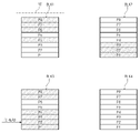
도 4 내지 도 7은 도 3에 도시된 방법에 따라 읽기 리클레임이 수행되는 과정을 보여주는 도면들이다. 도 1 및 도 4를 참조하면, 제1 내지 제4 메모리 블록들(BLK1~BLK4)이 도시된다. 제1 메모리 블록(BLK1)의 제1 내지 제4 페이지들(P1~P4) 및 제6 내지 제8 페이지들(P6~P8)은 유효 데이터를 저장할 수 있다. 제3 메모리 블록(BLK3)의 제1 내지 제4 페이지들(P1~P4) 및 제7 및 제8 페이지들(P7, P8)은 유효 데이터를 저장할 수 있다.4 to 7 are diagrams illustrating a process of performing a read reclaim according to the method illustrated in FIG. 3 . 1 and 4 , first to fourth memory blocks BLK1 to BLK4 are illustrated. The first to fourth pages P1 to P4 and the sixth to eighth pages P6 to P8 of the first memory block BLK1 may store valid data. The first to fourth pages P1 to P4 and the seventh and eighth pages P7 and P8 of the third memory block BLK3 may store valid data.
제1 메모리 블록(BLK1)은 이전에 읽기 리클레임의 대상 메모리 블록들(RT)로 등록된 것으로 가정된다. 또한, 대상 메모리 블록들(RT)과 연관된 카피 데이터의 양(CD)은 3개의 페이지들인 것으로 가정된다.It is assumed that the first memory block BLK1 has been previously registered as the target memory blocks RT of the read reclaim. Also, it is assumed that the amount of copy data CD associated with the target memory blocks RT is three pages.
제1 단계(①)에서, 외부의 호스트 장치 또는 컨트롤러(120)의 내부의 스케줄에 따라, 제1 메모리 블록(BLK1)의 제1 페이지(P1)에 대한 읽기가 요청될 수 있다. 컨트롤러(120)는 제1 메모리 블록(BLK1)의 제1 페이지(P1)에 기입될 데이터를 읽고, 외부의 호스트 장치로 출력하거나 또는 내부의 스케줄에 따라 사용할 수 있다.In the first step (①), a read of the first page P1 of the first memory block BLK1 may be requested according to an internal schedule of the external host device or the
읽기 리클레임의 대상 메모리 블록들(RT)에 대한 읽기가 수행되었으므로, 제2 단계(②)에서, 읽기 리클레임의 대상 메모리 블록들(RT)에 대해 한 번의 마이그레이션 동작(MIG)이 수행된다. 카피 데이터의 양(CD)에 해당하는 제1 내지 제3 페이지들(P1~P3)에 저장된 유효 데이터가 제2 메모리 블록(BLK2)으로 마이그레이션된다. Since the read of the target memory blocks RT of the read reclaim is performed, in the second step (②), one migration operation MIG is performed on the target memory blocks RT of the read reclaim. Valid data stored in the first to third pages P1 to P3 corresponding to the amount of copy data CD is migrated to the second memory block BLK2.
도 1 및 도 5를 참조하면, 제1 메모리 블록(BLK1)의 제1 내지 제3 페이지들(P1~P3)에 저장된 유효 데이터는 제2 메모리 블록(BLK2)의 제1 내지 제3 페이지들(P1~P3)로 마이그레이션될 수 있다.1 and 5 , valid data stored in the first to third pages P1 to P3 of the first memory block BLK1 may be stored in the first to third pages P1 to P3 of the second memory block BLK2. P1~P3) can be migrated.
제3 단계(③)에서, 제3 메모리 블록(BLK3)의 제2 페이지(P2)에 대한 읽기가 수행될 수 있다. 제3 메모리 블록(BLK3)은 읽기 리클레임의 대상 메모리 블록들(RT)에 속하지 않으므로, 제3 단계(③)의 읽기가 수행되어도 마이그레이션 동작은 수행되지 않는다.In the third step (③), reading of the second page P2 of the third memory block BLK3 may be performed. Since the third memory block BLK3 does not belong to the target memory blocks RT of the read reclaim, the migration operation is not performed even when the read in the third step (③) is performed.
예시적으로, 제3 단계(③)의 읽기가 수행되면, 도 1 및 도 6에 도시된 바와 같이, 제3 메모리 블록(BLK3)이 읽기 리클레임의 대상 메모리 블록들(RT)로 등록될 수 있다. 예를 들어, 도 2에 도시된 바와 같이, 제3 단계(③)의 읽기 시에, 에러 비트들의 수(NOEB)가 임계값(VCR) 이상일 수 있다. 제3 메모리 블록(BLK3)이 읽기 리클레임의 대상 메모리 블록들(RT)로 추가됨에 따라, 카피 데이터의 양(CD)이 다시 계산될 수 있다. 예시적으로, 카피 데이터의 양(CD)은 4개의 페이지들로 계산될 수 있다.Exemplarily, when the read of the third step (③) is performed, as shown in FIGS. 1 and 6 , the third memory block BLK3 may be registered as the target memory blocks RT of the read reclaim. have. For example, as shown in FIG. 2 , in reading in the third step (③), the number of error bits NOEB may be greater than or equal to the threshold value VCR. As the third memory block BLK3 is added as the target memory blocks RT of the read reclaim, the amount of copy data CD may be recalculated. For example, the amount of copy data (CD) may be calculated as 4 pages.
제4 단계(④)에서, 제3 메모리 블록(BLK3)의 제7 페이지(P7)에 대해 읽기가 수행될 수 있다. 제3 메모리 블록(BLK3)은 읽기 리클레임의 대상 메모리 블록들(RT)에 속하므로, 읽기 리클레임의 대상 메모리 블록들(RT)에 대해 한 번의 마이그레이션 동작이 수행될 수 있다. 예시적으로, 제1 메모리 블록(BLK1)이 제3 메모리 블록(BLK3)보다 먼저 읽기 리클레임의 대상 메모리 블록들(RT)로 등록되었으므로, 제5 단계(⑤)에서, 제1 메모리 블록(BLK1)에 대해 한 번의 마이그레이션 동작(MIG)이 수행될 수 있다. 예를 들어, 카피 데이터의 양(CD)에 해당하는 제4 및 제6 내지 제8 페이지들(P4, P6~P8)에 저장된 유효 데이터가 제2 메모리 블록들(BLK2)로 마이그레이션될 수 있다.In the fourth step (④), reading may be performed on the seventh page P7 of the third memory block BLK3. Since the third memory block BLK3 belongs to the target memory blocks RT of the read reclaim, one migration operation may be performed on the target memory blocks RT of the read reclaim. Exemplarily, since the first memory block BLK1 is registered as the target memory blocks RT of the read reclaim before the third memory block BLK3, in a fifth step (⑤), the first memory block BLK1 ), one migration operation (MIG) may be performed. For example, valid data stored in the fourth and sixth to eighth pages P4 and P6 to P8 corresponding to the amount of copy data CD may be migrated to the second memory blocks BLK2 .
도 1 및 도 7을 참조하면, 제1 메모리 블록(BLK1)의 제4 및 제6 내지 제8 페이지들(P4, P6~P8)은 제2 메모리 블록(BLK2)의 제4 내지 제7 페이지들(P4~P7)로 마이그레이션될 수 있다.1 and 7 , the fourth and sixth to eighth pages P4 and P6 to P8 of the first memory block BLK1 are the fourth to seventh pages of the second memory block BLK2 . It can be migrated to (P4~P7).
제5 단계(⑤)의 마이그레이션 동작(MIG)이 수행되면, 제1 메모리 블록(BLK1)에 유효 데이터는 존재하지 않는다. 즉, 제1 메모리 블록(BLK1)의 유효 데이터가 완료되며, 제1 메모리 블록(BLK1)의 읽기 리클레임이 완료된다. 따라서, 컨트롤러(120)는 제1 메모리 블록(BLK1)을 읽기 리클레임의 대상 메모리 블록들(RT)로부터 해제(release)할 수 있다.When the migration operation MIG of the fifth step ( ) is performed, valid data does not exist in the first memory block BLK1 . That is, the valid data of the first memory block BLK1 is completed, and the read reclaim of the first memory block BLK1 is completed. Accordingly, the
예시적으로, 제1 메모리 블록(BLK1)이 읽기 리클레임의 대상 메모리 블록들(RT)로부터 해제됨에 따라, 컨트롤러(120)는 카피 데이터의 양(CD)을 다시 계산할 수 있다.For example, as the first memory block BLK1 is released from the target memory blocks RT of the read reclaim, the
도 8은 컨트롤러(120)가 카피 데이터의 양(CD)을 다시 계산하는 제1 예를 보여주는 순서도이다. 도 1 및 도 8을 참조하면, S310 단계에서, 컨트롤러(120)는 읽기 리클레임의 대상 메모리 블록들(RT) 중 하나의 메모리 블록의 읽기 리클레임이 완료되었는지 판별한다. 읽기 리클레임이 완료되었으면, S320 단계에서, 컨트롤러(120)는 읽기 리클레임의 대상 메모리 블록들(RT)이 존재하는지 판별된다. 읽기 리클레임의 대상 메모리 블록들(RT)이 존재하면, S330 단계에서, 컨트롤러(120)는 읽기 리클레임의 대상 메모리 블록들(RT)의 카피 데이터의 양(CD)을 수학식 1에 따라 계산할 수 있다.8 is a flowchart illustrating a first example in which the
도 9는 카피 데이터의 양(CD)을 계산하고, 카피 데이터의 양(CD)에 기반하여 읽기 리클레임을 수행하는 제2 예를 보여주는 순서도이다. 도 1 및 도 9를 참조하면, S410 단계에서, 컨트롤러(120)는 트리거된 읽기 리클레임이 새로운 읽기 리클레임인지 판별한다.9 is a flowchart illustrating a second example of calculating the amount of copy data (CD) and performing read reclaim based on the amount of copy data (CD). 1 and 9 , in step S410 , the
S420 단계에서, 컨트롤러(120)는 읽기 리클레임의 대상 메모리 블록들(RT)의 카피 데이터의 양(CD)을 계산한다. 컨트롤러(120)는 수학식 2에 따라 카피 데이터의 양(CD)을 계산할 수 있다.In step S420 , the

수학식 2에서, 블록 카운트(BC)는 읽기 리클레임의 대상 메모리 블록들의 수를 가리킨다. 유효 카운트(VCDi)는 제i 대상 메모리 블록의 유효 데이터의 양, 예를 들어 유효 페이지들의 수를 가리킨다. 신뢰성 마진(RMi)은 제i 대상 메모리 블록의 데이터가 소실되지 않고 제i 대상 메모리 블록에서 수행될 수 있는 읽기 회수를 가리킨다. 읽기 교란(RD)은 외부의 호스트로부터 수신되는 읽기 요청에 따라 불휘발성 메모리 장치(110)의 메모리 블록에서 발생하는 읽기 교란을 수치화한 값일 수 있다.In Equation 2, the block count BC indicates the number of target memory blocks of read reclaim. The valid count VCDi indicates the amount of valid data of the ith target memory block, for example, the number of valid pages. The reliability margin RMi indicates the number of reads that can be performed on the ith target memory block without losing data of the ith target memory block. The read disturbance RD may be a numerical value of a read disturbance occurring in a memory block of the
예시적으로, 컨트롤러(120)는 불휘발성 메모리 장치(110)로부터 데이터를 읽을 때에, 페이지(P)의 단위로 읽을 수 있다. 외부의 호스트 장치는 호스트 액세스 단위에 기반하여 컨트롤러(120)에 읽기 요청을 전송할 수 있다. 예를 들어, 외부의 호스트 장치는 한 번의 읽기 요청을 통해 호스트 액세스 단위의 데이터를 읽을 것을 컨트롤러(120)에 요청할 수 있다. 호스트 액세스 단위의 사이즈는 둘 이상의 페이지들의 사이즈에 대응할 수 있다. 즉, 외부의 호스트 장치가 컨트롤러(120)에 하나의 읽기 요청을 전달하면, 컨트롤러(120)는 불휘발성 메모리 장치(110)에 대해 둘 이상의 읽기들을 수행할 수 있다.For example, when reading data from the
읽기 교란(RD)은 하나의 읽기 요청에 따라 발생하는 불휘발성 메모리 장치(110)에 대한 둘 이상의 읽기들이 읽기 리클레임의 대상 메모리 블록들(RT)에 속한 하나의 메모리 블록에 집중될 때에 발생하는 읽기 교란을 가리킬 수 있다.The read disturbance RD occurs when two or more reads to the
S430 단계에서, 컨트롤러(120)는 외부의 호스트 장치로부터 읽기 요청이 수신되는지 판별한다. 외부의 호스트 장치로부터 읽기 요청이 수신되면, S440 단계에서, 컨트롤러(120)는 카피 데이터의 양(CD)에 기반하여 읽기 리클레임의 대상 메모리 블록의 유효 데이터를 마이그레이션 동작에 의해 마이그레이션한다.In step S430 , the
도 9를 참조하여 설명된 방법에 따르면, 컨트롤러(120)는 외부의 호스트 장치로부터 수신되는 읽기 요청이 읽기 리클레임의 대상 메모리 블록들(RT)에 대한 읽기를 유발하는지를 참조하지 않는다. 컨트롤러(120)는 외부의 호스트 장치에 의해 요청된 읽기들이 읽기 리클레임의 대상 메모리 블록들(RT)에 속한 하나의 메모리 블록에 집중되는 워스트(worst) 케이스에 기반하여 카피 데이터의 양(CD)을 결정할 수 있다.According to the method described with reference to FIG. 9 , the
예시적으로, 도 8을 참조하여 설명된 바와 같이, 읽기 리클레임의 대상 메모리 블록들(RT)에 속한 하나의 메모리 블록의 읽기 리클레임이 완료될 때, 수학식 2에 따라 카피 데이터의 양(CD)이 다시 계산될 수 있다.Exemplarily, as described with reference to FIG. 8 , when the read reclaim of one memory block belonging to the target memory blocks RT of the read reclaim is completed, according to Equation 2, the amount of copy data ( CD) can be recalculated.
도 10은 컨트롤러(120)가 카피 데이터의 양(CD)을 계산하는 다른 예를 보여주는 순서도이다. 도 1 및 도 10을 참조하면, S510 단계에서, 컨트롤러(120)는 트리거된 읽기 리클레임이 새로운 읽기 리클레임인지 판별한다.10 is a flowchart illustrating another example in which the
트리거된 읽기 리클레임이 새로운 읽기 리클레임이면, S520 단계에서, 컨트롤러(120)는 새로운 읽기 리클레임에 대응하는 메모리 블록의 로컬 카피 데이터의 양(LCD)을 계산한다. 로컬 카피 데이터의 양(CD)은 읽기 리클레임의 대상 메모리 블록들(RT) 전체가 아닌, 새롭게 읽기 리클레임이 트리거된 메모리 블록에 대해 계산되는 값일 수 있다. 예를 들어, 로컬 카피 데이터의 양(LCD)은 수학식 1 또는 수학식 2에서 블록 카운트(BC)를 '1'로 설정함으로써 계산될 수 있다.If the triggered read reclaim is a new read reclaim, in step S520 , the
S530 단계에서, 컨트롤러(120)는 글로벌 카피 데이터의 양(GCD)을 갱신할 수 있다. 예를 들어, 글로벌 카피 데이터의 양(GCD)은 읽기 리클레임의 대상 메모리 블록들(RT) 전체에 대해 계산되는 값일 수 있다. 예를 들어, 컨트롤러(120)는 글로벌 카피 데이터의 양(GCD)에 새로 계산된 로컬 카피 데이터의 양(LCD)을 합함으로써, 글로벌 카피 데이터의 양(GCD)을 갱신할 수 있다.In step S530 , the
S540 단계에서, 컨트롤러(120)는 읽기 리클레임의 대상 메모리 블록들(RT) 중 하나의 메모리 블록의 읽기 리클레임이 완료되었는지 판별한다. 하나의 메모리 블록의 읽기 리클레임이 완료되었으면, S550 단계에서, 컨트롤러(120)는 글로벌 카피 데이터의 양(GCD)을 갱신한다. 예를 들어, 컨트롤러(120)는 글로벌 카피 데이터의 양(GCD)으로부터 읽기 리클레임이 완료된 메모리 블록의 로컬 카피 데이터의 양(LCD)을 감함으로써, 글로벌 카피 데이터의 양(GCD)을 갱신할 수 있다.In operation S540 , the
도 10에 도시된 방법에 따라 글로컬 카피 데이터의 양(GCD)을 관리하며, 컨트롤러(120)는 읽기 리클레임을 수행할 수 있다. 예를 들어, 수학식 1에 따라 로컬 카피 데이터의 양(LCD)이 계산될 수 있다. 컨트롤러(120)는 읽기 리클레임의 대상 메모리 블록들(RT)에 대한 읽기가 수행될 때, 글로벌 카피 데이터의 양(GCD)에 기반하여 한 번의 마이그레이션 동작을 수행할 수 있다. 다른 예로서, 수학식 2에 따라 로컬 카피 데이터의 양(LCD)이 계산될 수 있다. 컨트롤러(120)는 외부의 호스트 장치로부터 읽기 요청이 수신될 때, 글로벌 카피 데이터의 양(GCD)에 기반하여 한 번의 마이그레이션 동작을 수행할 수 있다.The amount of glocal copy data (GCD) is managed according to the method illustrated in FIG. 10 , and the
다시 도 1을 참조하면, 불휘발성 메모리 장치(110)는 컨트롤러(120)의 제어에 따라 쓰기, 읽기 및 소거를 수행할 수 있다. 불휘발성 메모리 장치(110)는 입출력 채널을 통해 컨트롤러(120)로부터 커맨드 및 어드레스를 수신할 수 있다. 불휘발성 메모리 장치(110)는 입출력 채널을 통해 컨트롤러(120)와 데이터를 교환할 수 있다.Referring back to FIG. 1 , the
불휘발성 메모리 장치(110)는 제어 채널을 통해 컨트롤러(120)와 제어 신호를 교환할 수 있다. 예를 들어, 불휘발성 메모리 장치(110)는 불휘발성 메모리 장치(110)의 복수의 불휘발성 메모리 칩들 중 적어도 하나의 불휘발성 메모리 칩을 선택하는 칩 인에이블 신호(/CE), 컨트롤러(120)로부터 입출력 채널을 통해 수신되는 신호가 커맨드임을 가리키는 커맨드 래치 인에이블 신호(CLE), 컨트롤러(120)로부터 입출력 채널을 통해 수신되는 신호가 어드레스임을 가리키는 어드레스 래치 인에이블 신호(ALE), 읽기 시에 컨트롤러(120)에 의해 생성되며 주기적으로 토글되어 타이밍을 맞추는 데에 사용되는 읽기 인에이블 신호(/RE), 커맨드 또는 어드레스가 전송될 때에 컨트롤러(120)에 의해 활성화되는 쓰기 인에이블 신호(/WE), 전원이 변화할 때에 의도하지 않은 쓰기 또는 소거를 방지하기 위해 컨트롤러(120)에 의해 활성화되는 쓰기 방지 신호(/WP), 쓰기 시에 컨트롤러(120)에 의해 생성되며 주기적으로 토글되어 입출력 채널을 통해 전달되는 데이터의 싱크를 맞추는 데에 사용되는 데이터 스트로브 신호(DQS)를 컨트롤러(120)로부터 수신할 수 있다. 예를 들어, 불휘발성 메모리 장치(110)는 불휘발성 메모리 장치(110)가 프로그램, 소거 또는 읽기 동작을 수행중인지를 가리키는 레디 및 비지 신호(R/nB), 불휘발성 메모리 장치(110)에 의해 읽기 인에이블 신호(/RE)로부터 생성되며 주기적으로 토글되어 데이터의 출력 싱크를 맞추는 데에 사용되는 데이터 스트로브 신호(DQS)를 컨트롤러(120)로 출력할 수 있다.The
불휘발성 메모리 장치(110)는 플래시 메모리를 포함할 수 있다. 그러나, 불휘발성 메모리 장치(110)는 플래시 메모리를 포함하는 것으로 한정되지 않는다. 불휘발성 메모리 장치(110)는 PRAM (Phase-change RAM), MRAM (Magnetic RAM), RRAM (Resistive RAM), FeRAM (Ferroelectric RAM) 등과 같은 다양한 불휘발성 메모리 장치들 중 적어도 하나를 포함할 수 있다.The
컨트롤러(120)는 불휘발성 메모리 장치(110)를 제어하도록 구성된다. 예를 들어, 컨트롤러(120)는 불휘발성 메모리 장치(110)가 쓰기, 읽기 또는 소거를 수행하도록 입출력 채널 및 제어 채널을 통해 불휘발성 메모리 장치(110)를 제어할 수 있다.The
컨트롤러(120)는 외부의 호스트 장치(미도시)의 제어에 따라 불휘발성 메모리 장치(110)를 제어할 수 있다. 예를 들어, 컨트롤러(120)는 불휘발성 메모리 장치(110)와 통신하는 포맷과 다른 포맷에 따라 외부의 호스트 장치와 통신할 수 있다. 컨트롤러(120)가 불휘발성 메모리 장치(110)와 통신하는 데이터의 단위는 외부의 호스트 장치와 통신하는 데이터의 단위와 다를 수 있다.The
컨트롤러(120)는 RAM (130)을 버퍼 메모리, 캐시 메모리, 또는 동작 메모리로 사용할 수 있다. 컨트롤러(120)는 불휘발성 메모리 장치(110)를 관리하기 위해 필요한 데이터 또는 코드를 RAM (130)에 저장할 수 있다. 예를 들어, 컨트롤러(120)는 불휘발성 메모리 장치(110)를 관리하기 위해 필요한 데이터 또는 코드를 불휘발성 메모리 장치(110)로부터 읽고, RAM (130)에 로딩하여 구동할 수 있다.The
RAM (130)은 DRAM (Dynamic RAM), SRAM (Static RAM), SDRAM (Synchronous DRAM), PRAM (Phase-change RAM), MRAM (Magnetic RAM), RRAM (Resistive RAM), FeRAM (Ferroelectric RAM) 등과 같은 다양한 랜덤 액세스 메모리 장치들 중 적어도 하나를 포함할 수 있다.
불휘발성 메모리 장치(110)는 복수의 불휘발성 메모리 칩들을 포함할 수 있다. 예시적으로, 컨트롤러(120) 및 불휘발성 메모리 칩들은 채널 및 웨이(way)에 기반하여 서로 연결될 수 있다. 하나의 채널은 하나의 데이터 채널 및 하나의 제어 채널을 포함할 수 있다. 하나의 데이터 채널은 8개의 데이터 라인들을 포함할 수 있다. 하나의 제어 채널은 상술된 칩 인에이블 신호(/CE), 커맨드 래치 인에이블 신호(CLE), 어드레스 래치 인에이블 신호(ALE), 읽기 인에이블 신호(/RE), 쓰기 인에이블 신호(/WE), 쓰기 방지 신호(/WP), 그리고 레디 및 비지 신호(R/nB)를 전송하는 제어 라인들을 포함할 수 있다.The
하나의 채널에 연결된 불휘발성 메모리 칩들은 웨이를 형성할 수 있다. 하나의 채널에 n개의 불휘발성 메모리 칩들이 연결되면, n-웨이(n-way)를 형성할 수 있다. 하나의 웨이에 속한 불휘발성 메모리 칩들은 데이터 라인들, 그리고 커맨드 래치 인에이블 신호(CLE), 어드레스 래치 인에이블 신호(ALE), 읽기 인에이블 신호(/RE), 쓰기 인에이블 신호(/WE), 그리고 쓰기 방지 신호(/WP)를 전송하는 제어 라인들을 공유할 수 있다. 하나의 웨이에 속한 불휘발성 메모리 칩들 각각은 칩 인에이블 신호(/CE), 그리고 레디 및 비지 신호(R/nB)를 전송하는 전용의 제어 라인들을 통해 컨트롤러(120)와 통신할 수 있다.Nonvolatile memory chips connected to one channel may form a way. When n nonvolatile memory chips are connected to one channel, an n-way may be formed. Nonvolatile memory chips belonging to one way have data lines, and a command latch enable signal (CLE), an address latch enable signal (ALE), a read enable signal (/RE), and a write enable signal (/WE). , and control lines that transmit a write-protect signal (/WP) may be shared. Each of the nonvolatile memory chips belonging to one way may communicate with the
컨트롤러(120)는 하나의 채널에 연결된 n-웨이의 불휘발성 메모리 칩들을 교대로 액세스할 수 있다. 컨트롤러(120)는 서로 다른 채널들에 연결된 불휘발성 메모리 칩들을 독립적으로 액세스할 수 있다. 컨트롤러(120)는 서로 다른 채널에 연결된 불휘발성 메모리 칩들을 교대로 또는 동시에 액세스할 수 있다.The
예시적으로, 불휘발성 메모리 칩들은 와이드IO (Wide IO) 형태로 컨트롤러(120)와 연결될 수 있다. 예를 들어, 서로 다른 채널들에 연결된 불휘발성 메모리 칩들이 하나의 칩 인에이블 신호(/CE)의 제어 라인을 공유할 수 있다. 하나의 칩 인에이블 신호(/CE)의 제어 라인을 공유하는 불휘발성 메모리 칩들은 동시에 액세스될 수 있다. 서로 다른 채널들의 데이터 라인들이 동시에 사용되므로, 넓은 입출력 대역폭이 달성될 수 있다.For example, the nonvolatile memory chips may be connected to the
스토리지 장치(100)는 솔리드 스테이트 드라이브(SSD, Solid State Drive) 또는 하드 디스크 드라이브(HDD, Hard Disk Drive)를 포함할 수 있다. 스토리지 장치(100)는 PC 카드(PCMCIA, personal computer memory card international association), 컴팩트 플래시 카드(CF), 스마트 미디어 카드(SM, SMC), 메모리 스틱, 멀티미디어 카드(MMC, RS-MMC, MMCmicro), SD 카드(SD, miniSD, microSD, SDHC), USB (Universal Serial Bus) 메모리 카드, 유니버설 플래시 스토리지(UFS) 등과 같은 메모리 카드들을 포함할 수 있다. 스토리지 장치(100)는 eMMC (embedded MultiMedia Card), UFS, PPN (Perfect Page NAND) 등과 같은 실장형 메모리를 포함할 수 있다.The
도 1에서, 스토리지 장치(100)는 컨트롤러(120)의 외부에 배치되는 RAM (130)을 포함하는 것으로 도시되어 있다. 그러나, 스토리지 장치(100)는 컨트롤러(120)의 외부에 배치되는 RAM (130)을 구비하지 않을 수 있다. 컨트롤러(120)는 내부의 RAM (도 11 참조)을 버퍼 메모리, 동작 메모리 또는 캐시 메모리로 사용하도록 구성될 수 있다.In FIG. 1 , the
도 11은 본 발명의 실시 예에 따른 컨트롤러(120)를 보여주는 블록도이다. 도 1 및 도 11을 참조하면, 컨트롤러(120)는 버스(121), 프로세서(122), RAM (123), 에러 정정 블록(124), 호스트 인터페이스(125), 버퍼 컨트롤 회로(126), 그리고 메모리 인터페이스(127)를 포함한다.11 is a block diagram showing the
버스(121)는 컨트롤러(120)의 구성 요소들 사이에 채널을 제공하도록 구성된다.
프로세서(122)는 컨트롤러(120)의 제반 동작을 제어하고, 논리 연산을 수행할 수 있다. 프로세서(122)는 호스트 인터페이스(125)를 통해 외부의 호스트 장치와 통신하고, 메모리 인터페이스(127)를 통해 불휘발성 메모리 장치(110)와 통신하고, 그리고 버퍼 제어 회로(126)를 통해 RAM (130)과 통신할 수 있다. 프로세서(122)는 RAM (123)을 동작 메모리, 캐시 메모리 또는 버퍼 메모리로 사용하여 스토리지 장치(100)를 제어할 수 있다.The
프로세서(122)는 리클레임 계산기(RC)를 포함한다. 예를 들어, 리클레임 계산기(RC)는 하드웨어로 구현되어 프로세서(122) 내에 포함될 수 있다. 리클레임 계산기(RC)는 소프트웨어로 구현되어 프로세서(122)에 의해 실행될 수 있다. 리클레임 계산기(RC)는 하드웨어 및 소프트웨어가 조합된 형태로 구현될 수 있다.The
RAM (123)은 프로세서(122)의 동작 메모리, 캐시 메모리 또는 버퍼 메모리로 사용될 수 있다. RAM (123)은 프로세서(122)가 실행하는 코드들 및 명령들을 저장할 수 있다. RAM (123)은 프로세서(122)에 의해 처리되는 데이터를 저장할 수 있다. RAM (123)은 SRAM (Static RAM)을 포함할 수 있다.The
에러 정정 블록(124)은 에러 정정을 수행할 수 있다. 에러 정정 블록(124)은 메모리 인터페이스(127)를 통해 불휘발성 메모리 장치(110)에 기입될 데이터에 기반하여 에러 정정 인코딩을 수행할 수 있다. 에러 정정 인코딩된 데이터는 메모리 인터페이스(127)를 통해 불휘발성 메모리 장치(110)로 전달될 수 있다. 에러 정정 블록(124)은 불휘발성 메모리 장치(110)로부터 메모리 인터페이스(127)를 통해 수신되는 데이터에 대해 에러 정정 디코딩을 수행할 수 있다. 예시적으로, 에러 정정 블록(124)은 메모리 인터페이스(127)의 구성 요소로서 메모리 인터페이스(127)에 포함될 수 있다.The
호스트 인터페이스(125)는 프로세서(122)의 제어에 따라, 외부의 호스트 장치와 통신하도록 구성된다. 호스트 인터페이스(125)는 USB (Universal Serial Bus), SATA (Serial AT Attachment), SAS (Serial Attached SCSI), HSIC (High Speed Interchip), SCSI (Small Computer System Interface), PCI (Peripheral Component Interconnection), PCIe (PCI express), NVMe (NonVolatile Memory express), UFS (Universal Flash Storage), SD (Secure Digital), MMC (MultiMedia Card), eMMC (embedded MMC), DIMM (Dual In-line Memory Module), RDIMM (Registered DIMM), LRDIMM (Load Reduced DIMM) 등과 같은 다양한 통신 방식들 중 적어도 하나를 이용하여 통신하도록 구성될 수 있다.The
버퍼 제어 회로(126)는 프로세서(122)의 제어에 따라, RAM (130)을 제어하도록 구성된다.The
메모리 인터페이스(127)는 프로세서(122)의 제어에 따라, 불휘발성 메모리 장치(110)와 통신하도록 구성된다. 도 1을 참조하여 설명된 바와 같이, 메모리 인터페이스(127)는 입출력 채널을 통해 커맨드, 어드레스 및 데이터를 불휘발성 메모리 장치(110)와 통신할 수 있다. 메모리 인터페이스(127)는 제어 채널을 통해 제어 신호를 불휘발성 메모리 장치(110)와 통신할 수 있다.The
예시적으로, 스토리지 장치(100)에 RAM (130)이 제공되지 않는 경우, 컨트롤러(120)에 버퍼 제어 회로(126)가 제공되지 않을 수 있다.For example, when the
예시적으로, 프로세서(122)는 코드들을 이용하여 컨트롤러(120)를 제어할 수 있다. 프로세서(122)는 컨트롤러(120)의 내부에 제공되는 불휘발성 메모리 장치(예를 들어, Read Only Memory)로부터 코드들을 로드할 수 있다. 다른 예로서, 프로세서(122)는 불휘발성 메모리 장치(110)로부터 메모리 인터페이스(127)를 통해 코드들을 로드할 수 있다.For example, the
예시적으로, 컨트롤러(120)의 버스(121)는 제어 버스 및 데이터 버스로 구분될 수 있다. 데이터 버스는 컨트롤러(120) 내에서 데이터를 전송하고, 제어 버스는 컨트롤러(120) 내에서 커맨드, 어드레스와 같은 제어 정보를 전송하도록 구성될 수 있다. 데이터 버스와 제어 버스는 서로 분리되며, 상호간에 간섭하거나 영향을 주지 않을 수 있다. 데이터 버스는 호스트 인터페이스(125), 버퍼 제어 회로(126), 에러 정정 블록(124) 및 메모리 인터페이스(127)에 연결될 수 있다. 제어 버스는 호스트 인터페이스(125), 프로세서(122), 버퍼 제어 회로(126), RAM (123) 및 메모리 인터페이스(127)에 연결될 수 있다.For example, the
도 12는 본 발명의 실시 예에 따른 불휘발성 메모리 장치(110)를 보여주는 블록도이다. 도 1 및 도 12를 참조하면, 불휘발성 메모리 장치(110)는 메모리 셀 어레이(111), 행 디코더 회로(113), 페이지 버퍼 회로(115), 데이터 입출력 회로(117), 그리고 제어 로직 회로(119)를 포함한다.12 is a block diagram illustrating a
메모리 셀 어레이(111)는 복수의 메모리 블록들(BLK1~BLKz)을 포함한다. 각 메모리 블록은 복수의 메모리 셀들을 포함한다. 각 메모리 블록은 적어도 하나의 접지 선택 라인(GSL), 복수의 워드 라인들(WL), 그리고 적어도 하나의 스트링 선택 라인(SSL)을 통해 행 디코더 회로(113)에 연결될 수 있다. 각 메모리 블록은 복수의 비트 라인들(BL)을 통해 페이지 버퍼 회로(115)에 연결될 수 있다. 복수의 메모리 블록들(BLK1~BLKz)은 복수의 비트 라인들(BL)에 공통으로 연결될 수 있다. 복수의 메모리 블록들(BLK1~BLKz)의 메모리 셀들은 동일한 구조들을 가질 수 있다.The
예시적으로, 복수의 메모리 블록들(BLK1~BLKz) 각각은 소거 동작의 단위일 수 있다. 메모리 셀 어레이(111)의 메모리 셀들은 하나의 메모리 블록의 단위로 소거될 수 있다. 하나의 메모리 블록에 속한 메모리 셀들은 동시에 소거될 수 있다. 다른 예로서, 각 메모리 블록은 복수의 서브 블록들로 분할될 수 있다. 복수의 서브 블록들 각각은 소거 동작의 단위일 수 있다.For example, each of the plurality of memory blocks BLK1 to BLKz may be a unit of an erase operation. Memory cells of the
예시적으로, 복수의 메모리 블록들(BLK1~BLKz) 각각은 블록 어드레스에 의해 식별되는 물리적 저장 공간을 포함할 수 있다. 복수의 워드 라인들(WL) 각각은 행 어드레스에 의해 식별되는 물리적 저장 공간에 대응할 수 있다. 복수의 비트 라인들(BL) 각각은 열 어드레스에 의해 식별되는 물리적 저장 공간에 대응할 수 있다.For example, each of the plurality of memory blocks BLK1 to BLKz may include a physical storage space identified by a block address. Each of the plurality of word lines WL may correspond to a physical storage space identified by a row address. Each of the plurality of bit lines BL may correspond to a physical storage space identified by a column address.
행 디코더 회로(113)는 복수의 접지 선택 라인들(GSL), 복수의 워드 라인들(WL), 그리고 복수의 스트링 선택 라인들(SSL)을 통해 메모리 셀 어레이(111)에 연결된다. 행 디코더 회로(113)는 제어 로직 회로(119)의 제어에 따라 동작한다. 행 디코더 회로(113)는 컨트롤러(120)로부터 입출력 채널을 통해 수신되는 어드레스를 디코딩하고, 디코딩된 어드레스에 따라 스트링 선택 라인들(SSL), 워드 라인들(WL), 그리고 접지 선택 라인들(GSL)에 인가되는 전압들을 제어할 수 있다.The
예를 들어, 프로그램 시에, 행 디코더 회로(113)는, 어드레스에 의해 선택된 메모리 블록의 선택된 워드 라인에 프로그램 전압(VGPM)을 인가하고, 선택된 메모리 블록의 비선택된 워드 라인들에 패스 전압(VPASS)을 인가할 수 있다. 읽기 시에, 행 디코더 회로(113)는 어드레스에 의해 선택된 메모리 블록의 선택된 워드 라인에 선택 읽기 전압(VRD)을 인가하고, 선택된 메모리 블록의 비선택된 워드 라인들에 비선택 읽기 전압(VREAD)을 인가할 수 있다. 소거 시에, 행 디코더 회로(113)는 어드레스에 의해 선택된 메모리 블록의 워드 라인들에 소거 전압들(예를 들어, 접지 전압 또는 접지 전압과 유사한 레벨들을 갖는 저전압들)을 인가할 수 있다.For example, during programming, the
페이지 버퍼 회로(115)는 복수의 비트 라인들(BL)을 통해 메모리 셀 어레이(111)에 연결된다. 페이지 버퍼 회로(115)는 복수의 데이터 라인들(DL)을 통해 데이터 입출력 회로(117)와 연결된다. 페이지 버퍼 회로(115)는 제어 로직 회로(119)의 제어에 따라 동작한다.The
프로그램 시에, 페이지 버퍼 회로(115)는 메모리 셀들에 프로그램될 데이터를 저장할 수 있다. 저장된 데이터에 기반하여, 페이지 버퍼 회로(115)는 복수의 비트 라인들(BL)에 전압들을 인가할 수 있다. 예를 들어, 페이지 버퍼 회로(115)는 쓰기 드라이버로 기능할 수 있다. 읽기 시에, 페이지 버퍼 회로(115)는 비트 라인들(BL)의 전압들을 센싱하고, 센싱 결과를 저장할 수 있다. 예를 들어, 페이지 버퍼 회로(115)는 감지 증폭기로 기능할 수 있다.During programming, the
데이터 입출력 회로(117)는 복수의 데이터 라인들(DL)을 통해 페이지 버퍼 회로(115)와 연결된다. 데이터 입출력 회로(117)는 페이지 버퍼 회로(115)에 의해 읽힌 데이터를 입출력 채널을 통해 컨트롤러(120)로 출력하고, 컨트롤러(120)로부터 입출력 채널을 통해 수신되는 데이터를 페이지 버퍼 회로(115)로 전달할 수 있다. The data input/
제어 로직 회로(119)는 컨트롤러(120)로부터 입출력 채널을 통해 커맨를 수신하고, 제어 채널을 통해 제어 신호를 수신할 수 있다. 제어 로직 회로(119)는 제어 신호에 응답하여 입출력 채널을 통해 수신되는 커맨드를 수신하고, 입출력 채널을 통해 수신되는 어드레스는 행 디코더 회로(113)로 라우팅하고, 그리고 입출력 채널을 통해 수신되는 데이터를 데이터 입출력 회로(117)로 라우팅할 수 있다. 제어 로직 회로(119)는 수신된 커맨드를 디코딩하고, 디코딩된 커맨드에 따라 불휘발성 메모리 장치(110)를 제어할 수 있다.The
예시적으로, 읽기 시에, 제어 로직 회로(119)는 컨트롤러(120)로부터 제어 채널을 통해 수신되는 읽기 인에이블 신호(/RE)로부터 데이터 스트로브 신호(DQS)를 생성할 수 있다. 생성된 데이터 스트로브 신호(DQS)는 제어 채널을 통해 컨트롤러(120)로 출력될 수 있다. 쓰기 시에, 제어 로직 회로(119)는 컨트롤러(120)로부터 제어 채널을 통해 데이터 스트로브 신호(DQS)를 수신할 수 있다.For example, during reading, the
도 13은 본 발명의 실시 예에 따른 메모리 블록(BLKa)을 보여주는 회로도이다. 도 13을 참조하면, 메모리 블록(BLKa)은 복수의 셀 스트링들(CS11~CS21, CS12~CS22)을 포함한다. 복수의 셀 스트링들(CS11~CS21, CS12~CS22)은 행 방향(row direction) 및 열 방향(column direction)을 따라 배열되어, 행들 및 열들을 형성할 수 있다.13 is a circuit diagram illustrating a memory block BLKa according to an embodiment of the present invention. Referring to FIG. 13 , the memory block BLKa includes a plurality of cell strings CS11 to CS21 and CS12 to CS22. The plurality of cell strings CS11 to CS21 and CS12 to CS22 may be arranged in a row direction and a column direction to form rows and columns.
예를 들어, 행 방향(row direction)을 따라 배열된 셀 스트링들(CS11, CS12)은 제1 행을 형성하고, 행 방향(row direction)을 따라 배열된 셀 스트링들(CS21, CS22)은 제2 행을 형성할 수 있다. 열 방향(column direction)을 따라 배열된 셀 스트링들(CS11, CS21)은 제1 열을 형성하고, 열 방향(column direction)을 따라 배열된 셀 스트링들(CS12, CS22)은 제2 열을 형성할 수 있다.For example, the cell strings CS11 and CS12 arranged in the row direction form a first row, and the cell strings CS21 and CS22 arranged in the row direction are arranged in the second row. You can form 2 rows. The cell strings CS11 and CS21 arranged along the column direction form a first column, and the cell strings CS12 and CS22 arranged along the column direction form a second column. can do.
각 셀 스트링은 복수의 셀 트랜지스터들을 포함할 수 있다. 복수의 셀 트랜지스터들은 접지 선택 트랜지스터들(GST), 메모리 셀들(MC1~MC6), 그리고 스트링 선택 트랜지스터들(SSTa, SSTb)을 포함한다. 각 셀 스트링의 접지 선택 트랜지스터들(GST), 메모리 셀들(MC1~MC6), 그리고 스트링 선택 트랜지스터들(SSTa, SSTb)은 셀 스트링들(CS11~CS21, CS12~CS22)이 행들 및 열들을 따라 배열되는 평면(예를 들어, 메모리 블록(BLKa)의 기판 상의 평면)과 수직한 높이 방향으로 적층될 수 있다.Each cell string may include a plurality of cell transistors. The plurality of cell transistors include ground select transistors GST, memory cells MC1 to MC6 , and string select transistors SSTa and SSTb. The ground select transistors GST, the memory cells MC1 to MC6, and the string select transistors SSTa and SSTb of each cell string have the cell strings CS11 to CS21 and CS12 to CS22 arranged in rows and columns. They may be stacked in a height direction perpendicular to a plane to be used (eg, a plane on a substrate of the memory block BLKa).
복수의 셀 트랜지스터들은 절연막에 포획된 전하량에 따라 가변하는 문턱 전압들을 갖는 전하 포획형(charge trap type) 트랜지스터들일 수 있다.The plurality of cell transistors may be charge trap type transistors having threshold voltages that vary according to the amount of charge trapped in the insulating layer.
최하단의 접지 선택 트랜지스터들(GST)의 소스들은 공통 소스 라인(CSL)에 공통으로 연결될 수 있다.Sources of the lowermost ground select transistors GST may be commonly connected to the common source line CSL.
복수의 셀 스트링들(CS11~CS21, CS12~CS22)의 접지 선택 트랜지스터들(GST)의 제어 게이트들은 접지 선택 라인들(GSL1, GSL2)에 각각 연결될 수 있다. 예시적으로, 동일한 행의 접지 선택 트랜지스터들은 동일한 접지 선택 라인에 연결되고, 서로 다른 행의 접지 선택 트랜지스터들은 서로 다른 접지 선택 라인들에 연결될 수 있다. 예를 들어, 제1 행의 셀 스트링들(CS11, CS12)의 접지 선택 트랜지스터들(GST)은 제1 접지 선택 라인(GSL1)에 연결되고, 제2 행의 셀 스트링들(CS21, CS22)의 접지 선택 트랜지스터들(GST)은 제2 접지 선택 라인(GSL2)에 연결될 수 있다.Control gates of the ground selection transistors GST of the plurality of cell strings CS11 to CS21 and CS12 to CS22 may be respectively connected to the ground selection lines GSL1 and GSL2. For example, ground select transistors in the same row may be connected to the same ground select line, and ground select transistors in different rows may be connected to different ground select lines. For example, the ground select transistors GST of the cell strings CS11 and CS12 in the first row are connected to the first ground select line GSL1, and The ground select transistors GST may be connected to the second ground select line GSL2 .
기판(또는 접지 선택 트랜지스터들(GST))으로부터 동일한 높이(또는 순서)에 위치한 메모리 셀들의 제어 게이트들은 하나의 워드 라인에 공통으로 연결되고, 서로 다른 높이(또는 순서)에 위치한 메모리 셀들의 제어 게이트들은 서로 다른 워드 라인들(WL1~WL6)에 각각 연결될 수 있다. 예를 들어, 메모리 셀들(MC1)은 워드 라인(WL1)에 공통으로 연결된다. 메모리 셀들(MC2)은 워드 라인(WL2)에 공통으로 연결된다. 메모리 셀들(MC3)은 워드 라인(WL3)에 공통으로 연결된다. 메모리 셀들(MC4)은 워드 라인(WL4)에 공통으로 연결된다. 메모리 셀들(MC5)은 워드 라인(WL5)에 공통으로 연결된다. 메모리 셀들(MC6)은 워드 라인(WL6)에 공통으로 연결된다.Control gates of memory cells positioned at the same height (or order) from the substrate (or ground select transistors GST) are commonly connected to one word line, and control gates of memory cells positioned at different heights (or order) from each other may be respectively connected to different word lines WL1 to WL6. For example, the memory cells MC1 are commonly connected to the word line WL1. The memory cells MC2 are commonly connected to the word line WL2. The memory cells MC3 are commonly connected to the word line WL3. The memory cells MC4 are commonly connected to the word line WL4. The memory cells MC5 are commonly connected to the word line WL5. The memory cells MC6 are commonly connected to the word line WL6.
복수의 셀 스트링들(CS11~CS21, CS12~CS22)의 동일한 높이(또는 순서)의 제1 스트링 선택 트랜지스터들(SSTa)에서, 서로 다른 행의 제1 스트링 선택 트랜지스터들(SSTa)의 제어 게이트들은 서로 다른 스트링 선택 라인들(SSL1a~SSL2a)에 각각 연결된다. 예를 들어, 셀 스트링들(CS11, CS12)의 제1 스트링 선택 트랜지스터들(SSTa)은 스트링 선택 라인(SSL1a)에 공통으로 연결된다. 셀 스트링들(CS21, CS22)의 제1 스트링 선택 트랜지스터들(SSTa)은 스트링 선택 라인(SSL2a)에 공통으로 연결된다.In the first string select transistors SSTa of the same height (or order) of the plurality of cell strings CS11 to CS21 and CS12 to CS22, the control gates of the first string select transistors SSTa in different rows are They are respectively connected to different string selection lines SSL1a to SSL2a. For example, the first string select transistors SSTa of the cell strings CS11 and CS12 are commonly connected to the string select line SSL1a. The first string select transistors SSTa of the cell strings CS21 and CS22 are commonly connected to the string select line SSL2a.
복수의 셀 스트링들(CS11~CS21, CS12~CS22)의 동일한 높이(또는 순서)의 제2 스트링 선택 트랜지스터들(SSTb)에서, 서로 다른 행의 제2 스트링 선택 트랜지스터들(SSTb)의 제어 게이트들은 서로 다른 스트링 선택 라인들(SSL1b~SSL2b)에 각각 연결된다. 예를 들어, 셀 스트링들(CS11, CS12)의 제2 스트링 선택 트랜지스터들(SSTb)은 스트링 선택 라인(SSL1b)에 공통으로 연결된다. 셀 스트링들(CS21, CS22)의 제2 스트링 선택 트랜지스터들(SSTb)은 스트링 선택 라인(SSL2b)에 공통으로 연결된다.In the second string select transistors SSTb of the same height (or order) of the plurality of cell strings CS11 to CS21 and CS12 to CS22, the control gates of the second string select transistors SSTb in different rows are They are respectively connected to different string selection lines SSL1b to SSL2b. For example, the second string select transistors SSTb of the cell strings CS11 and CS12 are commonly connected to the string select line SSL1b. The second string select transistors SSTb of the cell strings CS21 and CS22 are commonly connected to the string select line SSL2b.
즉, 서로 다른 행의 셀 스트링들은 서로 다른 스트링 선택 라인들에 연결된다. 동일한 행의 셀 스트링들의 동일한 높이(또는 순서)의 스트링 선택 트랜지스터들은 동일한 스트링 선택 라인에 연결된다. 동일한 행의 셀 스트링들의 서로 다른 높이(또는 순서)의 스트링 선택 트랜지스터들은 서로 다른 스트링 선택 라인들에 연결된다.That is, cell strings of different rows are connected to different string selection lines. String select transistors of the same height (or order) of cell strings in the same row are connected to the same string select line. String select transistors of different heights (or orders) of cell strings in the same row are connected to different string select lines.
예시적으로, 동일한 행의 셀 스트링들의 스트링 선택 트랜지스터들은 하나의 스트링 선택 라인에 공통으로 연결될 수 있다. 예를 들어, 제1 행의 셀 스트링들(CS11, CS12)의 스트링 선택 트랜지스터들(SSTa, SSTb)은 하나의 스트링 선택 라인에 공통으로 연결될 수 있다. 제2 행의 샐 스트링들(CS21, CS22)의 스트링 선택 트랜지스터들(SSTa, SSTb)은 하나의 스트링 선택 라인에 공통으로 연결될 수 있다.For example, string select transistors of cell strings in the same row may be commonly connected to one string select line. For example, the string select transistors SSTa and SSTb of the cell strings CS11 and CS12 of the first row may be commonly connected to one string select line. The string select transistors SSTa and SSTb of the cell strings CS21 and CS22 of the second row may be commonly connected to one string select line.
복수의 셀 스트링들(CS11~CS21, CS12~CS22)의 열들은 서로 다른 비트 라인들(BL1, BL2)에 각각 연결된다. 예를 들어, 제1 열의 셀 스트링들(CS11~CS21)의 스트링 선택 트랜지스터들(SSTb)은 비트 라인(BL1)에 공통으로 연결된다. 제2 열의 셀 스트링들(CS12~CS22)의 스트링 선택 트랜지스터들(SST)은 비트 라인(BL2)에 공통으로 연결된다.Columns of the plurality of cell strings CS11 to CS21 and CS12 to CS22 are respectively connected to different bit lines BL1 and BL2. For example, the string select transistors SSTb of the cell strings CS11 to CS21 of the first column are commonly connected to the bit line BL1. The string select transistors SST of the cell strings CS12 to CS22 of the second column are commonly connected to the bit line BL2.
셀 스트링들(CS11, CS12)은 제1 플레인을 형성할 수 있다. 셀 스트링들(CS21, CS22)은 제2 플레인을 형성할 수 있다.The cell strings CS11 and CS12 may form a first plane. The cell strings CS21 and CS22 may form a second plane.
메모리 블록(BLKa)에서, 각 플레인의 각 높이의 메모리 셀들은 물리 페이지를 형성할 수 있다. 물리 페이지는 메모리 셀들(MC1~MC6)의 쓰기 및 읽기의 단위일 수 있다. 예를 들어, 스트링 선택 라인들(SSL1a, SSL1b, SSL2a, SSL2b)에 의해 메모리 블록(BLKa)의 하나의 플레인이 선택될 수 있다. 스트링 선택 라인들(SSL1a, SSL1b)이 턴-온 전압이 공급되고 스트링 선택 라인들(SSL2a, SSL2b)에 턴-오프 전압이 공급될 때, 제1 플레인의 셀 스트링들(CS11, CS12)이 비트 라인들(BL1, BL2)에 연결된다. 즉, 제1 플레인이 선택된다. 스트링 선택 라인들(SSL2a, SSL2b)에 턴-온 전압이 공급되고 스트링 선택 라인들(SSL1a, SSL1B)에 턴-오프 전압이 공급될 때, 제2 플레인의 셀 스트링들(CS21, CS22)이 비트 라인들(BL1, BL2)에 연결된다. 즉, 제2 플레인이 선택된다. 선택된 플레인에서, 워드 라인들(WL1~WL6)에 의해 메모리 셀들(MC)의 하나의 행이 선택될 수 있다. 선택된 행에서, 제2 워드 라인(WL2)에 선택 전압이 인가되고, 나머지 워드 라인들(WL1, WL3~WL6)에 비선택 전압이 인가될 수 있다. 즉, 스트링 선택 라인들(SSL1a, SSL1b, SSL2a, SSL2b) 및 워드 라인들(WL1~WL6)의 전압들을 조절함으로써, 제2 플레인의 제2 워드 라인(WL2)에 대응하는 물리 페이지가 선택될 수 있다. 선택된 물리 페이지의 메모리 셀들(MC2)에서, 쓰기 또는 읽기가 수행될 수 있다.In the memory block BLKa, memory cells of each height of each plane may form a physical page. A physical page may be a unit of writing and reading of the memory cells MC1 to MC6 . For example, one plane of the memory block BLKa may be selected by the string selection lines SSL1a, SSL1b, SSL2a, and SSL2b. When a turn-on voltage is supplied to the string selection lines SSL1a and SSL1b and a turn-off voltage is supplied to the string selection lines SSL2a and SSL2b, the cell strings CS11 and CS12 of the first plane are bit It is connected to the lines BL1 and BL2. That is, the first plane is selected. When a turn-on voltage is supplied to the string selection lines SSL2a and SSL2b and a turn-off voltage is supplied to the string selection lines SSL1a and SSL1B, the cell strings CS21 and CS22 of the second plane are bit It is connected to the lines BL1 and BL2. That is, the second plane is selected. In the selected plane, one row of the memory cells MC may be selected by the word lines WL1 to WL6. In the selected row, a selection voltage may be applied to the second word line WL2 , and a non-selection voltage may be applied to the remaining word lines WL1 , WL3 to WL6 . That is, by adjusting voltages of the string selection lines SSL1a, SSL1b, SSL2a, and SSL2b and the word lines WL1 to WL6, a physical page corresponding to the second word line WL2 of the second plane can be selected. have. Writing or reading may be performed in the memory cells MC2 of the selected physical page.
메모리 블록(BLKa)에서, 메모리 셀들(MC1~MC6)의 소거는 메모리 블록 단위 또는 서브 블록의 단위로 수행될 수 있다. 메모리 블록 단위로 소거가 수행될 때, 메모리 블록(BLKa)의 모든 메모리 셀들(MC)이 하나의 소거 요청(예를 들어, 외부의 메모리 컨트롤러로부터의 소거 요청)에 따라 동시에 소거될 수 있다. 서브 블록의 단위로 수행될 때, 메모리 블록(BLKa)의 메모리 셀들(MC1~MC6) 중 일부는 하나의 소거 요청(예를 들어, 외부의 메모리 컨트롤러로부터의 소거 요청)에 따라 동시에 소거되고, 나머지 일부는 소거 금지될 수 있다. 소거되는 메모리 셀들(MC)에 연결된 워드 라인에 저전압(예를 들어, 접지 전압 또는 접지 전압과 유사한 레벨을 갖는 저전압)이 공급되고, 소거 금지된 메모리 셀들(MC)에 연결된 워드 라인은 플로팅될 수 있다.In the memory block BLKa, the memory cells MC1 to MC6 may be erased in units of memory blocks or sub-blocks. When erasing is performed in units of memory blocks, all memory cells MC of the memory block BLKa may be simultaneously erased according to one erase request (eg, an erase request from an external memory controller). When performed in units of sub-blocks, some of the memory cells MC1 to MC6 of the memory block BLKa are simultaneously erased according to one erase request (eg, an erase request from an external memory controller), and the remaining Some may be erasable. A low voltage (eg, a ground voltage or a low voltage having a level similar to the ground voltage) is supplied to a word line connected to the erase-inhibited memory cells MC, and the word line connected to the erase-inhibited memory cells MC may be floated. have.
예시적으로, 메모리 블록(BLKa)은 블록 어드레스에 의해 식별되는 물리적 저장 공간을 포함할 수 있다. 워드 라인들(WL1~WL6) 각각은 행 어드레스에 의해 식별되는 물리적 저장 공간에 대응할 수 있다. 비트 라인들(BL1, BL2) 각각은 열 어드레스에 의해 식별되는 물리적 저장 공간에 대응할 수 있다. 서로 다른 행의 스트링 선택 라인들(SSL1a 및 SSL2a, 또는 SSL1b 및 SSL2b) 각각은 또는 서로 다른 행의 접지 선택 라인들(GSL1 및 GSL2)은 플레인 어드레스에 의해 식별되는 물리적 저장 공간에 대응할 수 있다.For example, the memory block BLKa may include a physical storage space identified by a block address. Each of the word lines WL1 to WL6 may correspond to a physical storage space identified by a row address. Each of the bit lines BL1 and BL2 may correspond to a physical storage space identified by a column address. Each of the string select lines SSL1a and SSL2a, or SSL1b and SSL2b in different rows or the ground select lines GSL1 and GSL2 in different rows may correspond to a physical storage space identified by a plane address.
도 13에 도시된 메모리 블록(BLKa)은 예시적인 것이다. 본 발명의 기술적 사상은 도 13에 도시된 메모리 블록(BLKa)에 한정되지 않는다. 예를 들어, 셀 스트링들의 행들의 수는 증가 또는 감소될 수 있다. 셀 스트링들의 행들의 수가 변경됨에 따라, 셀 스트링들의 행들에 연결되는 스트링 선택 라인들 또는 접지 선택 라인의 수, 그리고 하나의 비트 라인에 연결되는 셀 스트링들의 수 또한 변경될 수 있다.The memory block BLKa illustrated in FIG. 13 is exemplary. The technical concept of the present invention is not limited to the memory block BLKa shown in FIG. 13 . For example, the number of rows of cell strings may be increased or decreased. As the number of rows of cell strings is changed, the number of string select lines or ground select lines connected to the rows of cell strings and the number of cell strings connected to one bit line may also be changed.
셀 스트링들의 열들의 수는 증가 또는 감소될 수 있다. 셀 스트링들의 열들의 수가 변경됨에 따라, 셀 스트링들의 열들에 연결되는 비트 라인들의 수, 그리고 하나의 스트링 선택 라인에 연결되는 셀 스트링들의 수 또한 변경될 수 있다.The number of columns of cell strings may be increased or decreased. As the number of columns of the cell strings is changed, the number of bit lines connected to the columns of the cell strings and the number of cell strings connected to one string selection line may also be changed.
셀 스트링들의 높이는 증가 또는 감소될 수 있다. 예를 들어, 셀 스트링들 각각에 적층되는 접지 선택 트랜지스터들, 메모리 셀들 또는 스트링 선택 트랜지스터들의 수는 증가 또는 감소될 수 있다.The height of the cell strings may be increased or decreased. For example, the number of ground select transistors, memory cells, or string select transistors stacked on each of the cell strings may be increased or decreased.
예시적으로, 하나의 물리 페이지에 속한 메모리 셀들(MC)은 적어도 세 개의 논리 페이지들에 대응할 수 있다. 예를 들어, 하나의 메모리 셀(MC)에 k 개(k는 2보다 큰 양의 정수)의 비트들이 프로그램될 수 있다. 하나의 물리 페이지에 속한 메모리 셀들(MC)에서, 각 메모리 셀(MC)에 프로그램되는 k 개의 비트들은 각각 k 개의 논리 페이지들을 형성할 수 있다.For example, the memory cells MC belonging to one physical page may correspond to at least three logical pages. For example, k bits (k is a positive integer greater than 2) may be programmed in one memory cell MC. In the memory cells MC belonging to one physical page, k bits programmed in each memory cell MC may form k logical pages, respectively.
예를 들어, 하나의 물리 페이지는 블록 어드레스, 행 어드레스, 열 어드레스 및 플레인 어드레스에 의해 식별되는 물리적 저장 공간을 포함한다. 하나의 물리 페이지는 둘 이상의 논리 페이지들을 포함할 수 있다. 논리 페이지들 각각은 물리 페이지의 어드레스에 더하여 논리 페이지들을 식별하는 추가 어드레스(또는 오프셋)에 의해 식별되는 논리적 저장 공간을 포함할 수 있다.For example, one physical page includes a physical storage space identified by a block address, a row address, a column address, and a plane address. One physical page may include two or more logical pages. Each of the logical pages may include logical storage space identified by an additional address (or offset) identifying the logical pages in addition to the address of the physical page.
본 발명의 기술적 사상에 따른 일 예로서, 3차원 메모리 어레이가 제공된다. 3차원 메모리 어레이는, 실리콘 기판 및 메모리 셀들의 동작에 연관된 회로의 위에 배치되는 활성 영역을 갖는 메모리 셀들의 어레이들의 하나 또는 그 이상의 물리 레벨들에 획일적으로(monolithically) 형성될 수 있다. 메모리 셀들의 동작에 연관된 회로는 기판 내에 또는 기판 위에 위치할 수 있다. 획일적으로 형성되는 것은, 3차원 어레이의 각 레벨의 레이어들이 3차원 어레이의 하위 레벨의 레이어들 위에 직접 증착됨을 의미한다.As an example according to the technical spirit of the present invention, a three-dimensional memory array is provided. A three-dimensional memory array may be formed monolithically on one or more physical levels of an array of memory cells having an active area disposed over a silicon substrate and circuitry associated with operation of the memory cells. Circuitry involved in the operation of the memory cells may be located in or on the substrate. Being uniformly formed means that the layers of each level of the 3D array are directly deposited on the layers of the lower level of the 3D array.
본 발명의 기술적 사상에 따른 일 예로서, 3차원 메모리 어레이는 수직의 방향성을 가져, 적어도 하나의 메모리 셀이 다른 하나의 메모리 셀 위에 위치하는 수직 NAND 스트링들을 포함한다. 적어도 하나의 메모리 셀은 전하 포획 레이어를 포함한다. 각 수직 NAND 스트링은 메모리 셀들 위에 위치하는 적어도 하나의 선택 트랜지스터를 더 포함한다. 적어도 하나의 선택 트랜지스터는 메모리 셀들과 동일한 구조를 갖고, 메모리 셀들과 함께 획일적으로 형성된다.As an example according to the inventive concept, a 3D memory array has vertical directionality, and includes vertical NAND strings in which at least one memory cell is positioned on another memory cell. At least one memory cell includes a charge trap layer. Each vertical NAND string further includes at least one select transistor located above the memory cells. The at least one selection transistor has the same structure as the memory cells and is uniformly formed together with the memory cells.
3차원 메모리 어레이가 복수의 레벨들로 구성되고, 레벨들 사이에서 워드 라인들 또는 비트 라인들이 공유되는 구성은 미국등록특허공보 제7,679,133호, 미국등록특허공보 제8,553,466호, 미국등록특허공보 제8,654,587호, 미국등록특허공보 제8,559,235호, 그리고 미국공개특허공보 제2011/0233648호에 개시되어 있으며, 본 발명의 레퍼런스로 포함된다.A configuration in which a three-dimensional memory array is composed of a plurality of levels, and word lines or bit lines are shared between levels, is described in U.S. Patent No. 7,679,133, U.S. Patent No. 8,553,466, U.S. Patent No. 8,654,587 No. 8,559,235, and U.S. Patent Publication No. 2011/0233648, incorporated herein by reference.
도 14는 본 발명의 실시 예에 따른 컴퓨팅 장치(1000)를 보여주는 블록도이다. 도 14를 참조하면, 컴퓨팅 장치(1000)는 프로세서(1100), 메모리(1200), 스토리지 장치(1300), 모뎀(1400), 그리고 사용자 인터페이스(1500)를 포함한다.14 is a block diagram illustrating a
프로세서(1100)는 컴퓨팅 장치(1000)의 제반 동작을 제어하고, 논리 연산을 수행할 수 있다. 프로세서(1100)는 코드 또는 프로그램에 포함된 명령으로 표현되는 동작들을 실행하도록 물리적으로 구성된 회로를 포함하는 하드웨어 기반의 데이터 프로세싱 장치일 수 있다. 예를 들어, 프로세서(1100)는 시스템-온-칩(SoC, System-on-Chip)으로 구성될 수 있다. 프로세서(1100)는 범용 프로세서, 특수 목적 프로세서 또는 어플리케이션 프로세서일 수 있다.The
RAM (1200)은 프로세서(1100)와 통신할 수 있다. RAM (1200)은 프로세서(1100) 또는 컴퓨팅 장치(1000)의 메인 메모리일 수 있다. 프로세서(1100)는 RAM (1200)에 코드 또는 데이터를 임시로 저장할 수 있다. 프로세서(1100)는 RAM (1200)을 이용하여 코드를 실행하고, 데이터를 처리할 수 있다. 프로세서(1100)는 RAM (1200)을 이용하여 운영체제, 어플리케이션과 같은 다양한 소프트웨어들을 실행할 수 있다. 프로세서(1100)는 RAM (1200)을 이용하여 컴퓨팅 장치(1000)의 제반 동작을 제어할 수 있다. RAM (1200)은 SRAM (Static RAM), DRAM (Dynamic RAM), SDRAM (Synchronous DRAM) 등과 같은 휘발성 메모리, 또는 PRAM (Phase-change RAM), MRAM (Magnetic RAM), RRAM (Resistive RAM), FeRAM (Ferroelectric RAM) 등과 같은 불휘발성 메모리 장치를 포함할 수 있다.The
스토리지 장치(1300)는 프로세서(1100)와 통신할 수 있다. 스토리지 장치(1300)는 장기적으로 보존되어야 하는 데이터를 저장할 수 있다. 즉, 프로세서(1100)는 장기적으로 보존되어야 하는 데이터를 스토리지 장치(1300)에 저장할 수 있다. 스토리지 장치(1300)는 컴퓨팅 장치(1000)를 구동하기 위한 부트 이미지를 저장할 수 있다. 스토리지 장치(1300)는 운영체제, 어플리케이션과 같은 다양한 소프트웨어들의 소스 코드들을 저장할 수 있다. 스토리지 장치(1300)는 운영체제, 어플리케이션과 같은 다양한 소프트웨어들에 의해 처리된 데이터를 저장할 수 있다.The
예시적으로, 프로세서(1100)는 스토리지 장치(1300)에 저장된 소스 코드들을 RAM (1200)에 로드하고, RAM (1200)에 로드된 코드들을 실행함으로써, 운영체제, 어플리케이션과 같은 다양한 소프트웨어들을 구동할 수 있다. 프로세서(1100)는 스토리지 장치(1300)에 저장된 데이터를 RAM (1200)에 로드하고, RAM (1200)에 로드된 데이터를 처리할 수 있다. 프로세서(1100)는 RAM (1200)에 저장된 데이터 중 장기적으로 보존하고자 하는 데이터를 스토리지 장치(1300)에 저장할 수 있다.For example, the
스토리지 장치(1300)는 플래시 메모리, PRAM (Phase-change RAM), MRAM (Magnetic RAM), RRAM (Resistive RAM), FRAM (Ferroelectric RAM) 등과 같은 불휘발성 메모리 장치를 포함할 수 있다.The
모뎀(1400)은 프로세서(1100)의 제어에 따라 외부 장치와 통신을 수행할 수 있다. 예를 들어, 모뎀(1400)은 외부 장치와 유선 또는 무선 통신을 수행할 수 있다. 모뎀(140)은 LTE (Long Term Evolution), 와이맥스(WiMax), GSM (Global System for Mobile communication), CDMA (Code Division Multiple Access), 블루투스(Bluetooth), NFC (Near Field Communication), 와이파이(WiFi), RFID (Radio Frequency IDentification) 등과 같은 다양한 무선 통신 방식들, 또는 USB (Universal Serial Bus), SATA (Serial AT Attachment), HSIC (High Speed Interchip), SCSI (Small Computer System Interface), 파이어와이어(Firewire), PCI (Peripheral Component Interconnection), PCIe (PCI express), NVMe (NonVolatile Memory express), UFS (Universal Flash Storage), SD (Secure Digital), SDIO, UART (Universal Asynchronous Receiver Transmitter), SPI (Serial Peripheral Interface), HS-SPI (High Speed SPI), RS232, I2C (Inter-integrated Circuit), HS-I2C, I2S, (Integrated-interchip Sound), S/PDIF (Sony/Philips Digital Interface), MMC (MultiMedia Card), eMMC (embedded MMC) 등과 같은 다양한 유선 통신 방식들 중 적어도 하나에 기반하여 통신을 수행할 수 있다.The
사용자 인터페이스(1500)는 프로세서(1100)의 제어에 따라 사용자와 통신할 수 있다. 예를 들어, 사용자 인터페이스(1500)는 키보드, 키패드, 버튼, 터치 패널, 터치 스크린, 터치 패드, 터치 볼, 카메라, 마이크, 자이로스코프 센서, 진동 센서, 등과 같은 사용자 입력 인터페이스들을 포함할 수 있다. 사용자 인터페이스(150)는 LCD (Liquid Crystal Display), OLED (Organic Light Emitting Diode) 표시 장치, AMOLED (Active Matrix OLED) 표시 장치, LED, 스피커, 모터 등과 같은 사용자 출력 인터페이스들을 포함할 수 있다.The
스토리지 장치(1300)는 본 발명의 실시 예에 따른 스토리지 장치(100)를 포함할 수 있다. 프로세서(1100), RAM (1200), 모뎀(1400), 그리고 사용자 인터페이스(1500)는 스토리지 장치(1300)와 통신하는 호스트 장치를 형성할 수 있다.The
본 발명의 상세한 설명에서는 구체적인 실시 예에 관하여 설명하였으나, 본 발명의 범위와 기술적 사상에서 벗어나지 않는 한도 내에서 여러 가지 변형이 가능하다. 그러므로 본 발명의 범위는 상술한 실시 예에 국한되어 정해져서는 안되며 후술하는 특허청구범위뿐만 아니라 이 발명의 특허청구범위와 균등한 것들에 의해 정해져야 한다.In the detailed description of the present invention, specific embodiments have been described, but various modifications are possible without departing from the scope and technical spirit of the present invention. Therefore, the scope of the present invention should not be limited to the above-described embodiment, but should be defined by the claims described below as well as the claims and equivalents of the present invention.
100; 스토리지 장치 110; 불휘발성 메모리 장치
111; 메모리 셀 어레이 113; 행 디코더 회로
115; 페이지 버퍼 회로 117; 데이터 입출력 회로
119; 제어 로직 회로 120; 컨트롤러
RC: 리클레임 계산기 130; 랜덤 액세스 메모리(RAM)
121; 버스 122; 프로세서
123; 랜덤 액세스 메모리 124; 에러 정정 블록
125; 호스트 인터페이스 126; 버퍼 제어 회로
127; 메모리 인터페이스 1000; 컴퓨팅 장치
1100; 프로세서 1200; 랜덤 액세스 메모리
1300; 스토리지 장치 1400; 모뎀
1500; 사용자 인터페이스100;
111;
115;
119;
RC: Reclaim
121;
123;
125;
127;
1100;
1300;
1500; user interface
Claims (20)
상기 메모리 블록들 중 선택된 메모리 블록에 대해 쓰기, 읽기 및 소거를 수행하도록 구성되는 컨트롤러를 포함하고,
상기 선택된 메모리 블록에 대한 읽기 시에 에러 비트들의 수가 임계값 이상인 것에 기반하여, 상기 컨트롤러는 상기 선택된 메모리 블록에 저장된 유효 데이터를 적어도 두 개의 마이그레이션 동작들을 통해 다른 메모리 블록으로 마이그레이션(migration)하는 제1 읽기 리클레임을 수행하도록 구성되고,
상기 유효 데이터가 상기 다른 메모리 블록으로 마이그레이션 되는 것에 응답하여, 상기 유효 데이터는 상기 선택된 메모리 블록에 존재하지 않고,
상기 선택된 메모리 블록의 데이터를 소실하지 않고 상기 선택된 메모리 블록에서 수행될 수 있는 읽기 동작들의 회수를 가리키는 상기 선택된 메모리 블록의 신뢰성에 기반하여, 상기 제1 읽기 리클레임 시에, 상기 컨트롤러는 상기 적어도 두 개의 마이그레이션 동작들 중 한 번의 마이그레이션 동작 시에 마이그레이션 되는 데이터의 양을 조절하도록 구성되는 스토리지 장치.a nonvolatile memory device including memory blocks; and
a controller configured to write, read, and erase a selected memory block among the memory blocks;
Based on the number of error bits during reading of the selected memory block being equal to or greater than a threshold value, the controller is configured to perform a first migration of valid data stored in the selected memory block to another memory block through at least two migration operations. configured to perform read reclaim;
In response to the valid data being migrated to the other memory block, the valid data is not present in the selected memory block;
Based on the reliability of the selected memory block indicating the number of read operations that can be performed on the selected memory block without losing data of the selected memory block, in the first read reclaim, the controller A storage device configured to control the amount of data to be migrated during one migration operation among the number of migration operations.
상기 선택된 메모리 블록에 대한 제1 읽기 리클레임이 시작될 때에 이미 수행 중인 제2 읽기 리클레임이 존재하는 것에 기반하여, 상기 컨트롤러는 상기 제2 읽기 리클레임에서 상기 한 번의 마이그레이션 동작 동안 마이그레이션되는 상기 데이터의 양을 증가시키도록 구성되는 스토리지 장치.According to claim 1,
When the first read reclaim for the selected memory block starts, based on the presence of a second read reclaim that is already being performed, the controller controls the data migrated during the one migration operation in the second read reclaim. A storage device configured to increase the amount.
상기 수행 중인 제2 읽기 리클레임이 종료되는 것에 기반하여, 상기 컨트롤러는 상기 제1 읽기 리클레임에서 상기 한 번의 마이그레이션 동작 동안 마이그레이션 되는 상기 데이터의 양을 감소시키도록 구성되는 스토리지 장치.3. The method of claim 2,
The storage device is configured to reduce, in the first read reclaim, an amount of the data migrated during the one migration operation in the first read reclaim, based on the end of the second read reclaim being performed.
상기 선택된 메모리 블록의 신뢰성이 증가하는 것에 기반하여, 상기 컨트롤러는 상기 제1 읽기 리클레임에서 상기 한 번의 마이그레이션 동작 동안 마이그레이션 되는 상기 데이터의 양을 감소시키도록 구성되는 스토리지 장치.According to claim 1,
and the controller is configured to decrease the amount of the data migrated during the one migration operation in the first read reclaim, based on the increase in reliability of the selected memory block.
상기 선택된 메모리 블록의 신뢰성이 감소하는 것에 기반하여, 상기 컨트롤러는 상기 제1 읽기 리클레임에서 상기 한 번의 마이그레이션 동작 동안 마이그레이션 되는 상기 데이터의 양을 증가시키도록 구성되는 스토리지 장치.According to claim 1,
and the controller is configured to increase the amount of the data migrated during the one migration operation in the first read reclaim operation based on the decrease in reliability of the selected memory block.
상기 컨트롤러는 제3 읽기 리클레임의 대상인 대상 메모리 블록들 중 하나의 대상 메모리 블록에서 읽기가 수행되는 것에 기반하여, 상기 대상 메모리 블록들에 대해 상기 한 번의 마이그레이션 동작을 수행하도록 구성되는 스토리지 장치.According to claim 1,
and the controller is configured to perform the one migration operation on the target memory blocks based on a read being performed from one of the target memory blocks that are the target of the third read reclaim.
상기 컨트롤러는 외부의 호스트 장치로부터 읽기 요청이 수신되는 것에 기반하여, 제3 읽기 리클레임의 대상인 대상 메모리 블록들에 대해 상기 한 번의 마이그레이션 동작을 수행하도록 구성되는 스토리지 장치.According to claim 1,
and the controller is configured to perform the one-time migration operation on target memory blocks that are the target of a third read reclaim based on a read request being received from an external host device.
상기 선택된 메모리 블록의 상기 제1 읽기 리클레임이 시작될 때에 이미 수행 중인 제3 읽기 리클레임이 존재하는 것에 기반하여, 상기 컨트롤러는 상기 수행 중인 상기 제3 읽기 리클레임이 완료되는 것에 응답하여 상기 제1 읽기 리클레임을 시작하도록 구성되는 스토리지 장치.According to claim 1,
When the first read reclaim of the selected memory block starts, based on the presence of a third read reclaim that is already being performed, the controller is configured to perform the first read reclaim in response to the completion of the third read reclaim A storage device that is configured to initiate read reclaims.
상기 메모리 블록들 중 하나의 메모리 블록은 기판 위에 배열되는 셀 스트링들을 포함하고,
상기 셀 스트링들 각각은 상기 기판과 수직한 방향으로 적층되는 적어도 하나의 선택 트랜지스터 및 메모리 셀들을 포함하는 스토리지 장치.According to claim 1,
One memory block of the memory blocks includes cell strings arranged on a substrate;
Each of the cell strings includes at least one selection transistor and memory cells stacked in a direction perpendicular to the substrate.
상기 적어도 하나의 선택 트랜지스터 및 상기 메모리 셀들은 전하 포획층을 포함하는 스토리지 장치.10. The method of claim 9,
wherein the at least one select transistor and the memory cells include a charge trap layer.
메모리 블록들을 포함하는 불휘발성 메모리 장치; 그리고
상기 메모리 블록들 중 선택된 메모리 블록에 대해 쓰기, 읽기 및 소거를 수행하도록 구성되는 컨트롤러를 포함하고,
상기 선택된 메모리 블록에 대한 읽기 시에 에러 비트들의 수가 임계값 이상인 것에 기반하여, 상기 컨트롤러는 상기 선택된 메모리 블록에 저장된 유효 데이터를 읽고, 상기 유효 데이터를 상기 랜덤 액세스 메모리에 저장하고, 상기 랜덤 액세스 메모리에 저장된 상기 유효 데이터를 적어도 두 개의 마이그레이션 동작들을 통해 상기 불휘발성 메모리 장치의 다른 메모리 블록에 기입하는 제1 읽기 리클레임을 수행하도록 구성되고,
상기 유효 데이터가 상기 다른 메모리 블록에 기입되는 것에 응답하여, 상기 유효 데이터는 상기 선택된 메모리 블록에 존재하지 않고,
상기 선택된 메모리 블록의 데이터를 소실하지 않고 상기 선택된 메모리 블록에서 수행될 수 있는 읽기 동작들의 회수를 가리키는 상기 선택된 메모리 블록의 신뢰성에 기반하여, 상기 제1 읽기 리클레임 시에, 상기 컨트롤러는 상기 적어도 두 개의 마이그레이션 동작들 중 한 번의 마이그레이션 동작 시에 상기 선택된 메모리 블록으로부터 상기 다른 메모리 블록으로 마이그레이션(migration) 되는 데이터의 양을 조절하도록 구성되는 스토리지 장치.random access memory;
a nonvolatile memory device including memory blocks; and
a controller configured to write, read, and erase a selected memory block among the memory blocks;
Based on that the number of error bits in reading from the selected memory block is equal to or greater than a threshold value, the controller reads valid data stored in the selected memory block, stores the valid data in the random access memory, and the random access memory and perform a first read reclaim for writing the valid data stored in the memory block to another memory block of the nonvolatile memory device through at least two migration operations,
In response to the valid data being written to the other memory block, the valid data is not present in the selected memory block;
Based on the reliability of the selected memory block indicating the number of read operations that can be performed on the selected memory block without losing data of the selected memory block, in the first read reclaim, the controller The storage device is configured to adjust an amount of data migrated from the selected memory block to the other memory block during one migration operation among migration operations.
상기 랜덤 액세스 메모리, 상기 불휘발성 메모리 장치, 그리고 상기 컨트롤러는 솔리드 스테이트 드라이브(SSD, Solid State Drive)를 형성하는 스토리지 장치.12. The method of claim 11,
The random access memory, the nonvolatile memory device, and the controller form a solid state drive (SSD) storage device.
상기 컨트롤러는 상기 선택된 메모리 블록의 신뢰성의 증가에 기반하여 상기 마이그레이션 되는 상기 데이터의 양을 감소시키도록 구성되는 스토리지 장치.12. The method of claim 11,
and the controller is configured to decrease the amount of the migrated data based on an increase in reliability of the selected memory block.
상기 컨트롤러는 상기 선택된 메모리 블록의 소거 횟수, 상기 선택된 메모리 블록에 상기 유효 데이터가 기입된 후 경과한 시간, 그리고 상기 선택된 메모리 블록에 상기 유효 데이터가 기입될 때의 온도 및 상기 제1 읽기 리클레임이 수행될 때의 온도의 차이 중 적어도 하나에 기반하여 상기 마이그레이션 되는 상기 데이터의 양을 조절하도록 구성되는 스토리지 장치.12. The method of claim 11,
The controller determines the number of times the selected memory block is erased, the time elapsed after the valid data is written to the selected memory block, the temperature when the valid data is written to the selected memory block, and the first read reclaim and adjust the amount of the migrated data based on at least one of a difference in temperature when performed.
상기 컨트롤러는 상기 메모리 블록들 중에서 상기 제1 읽기 리클레임을 포함하는 제2 읽기 리클레임이 수행되는 전체 메모리 블록들의 전체 유효 데이터의 양에 기반하여 상기 마이그레이션 되는 상기 데이터의 양을 조절하도록 구성되는 스토리지 장치.12. The method of claim 11,
the controller is configured to adjust the amount of the migrated data based on a total amount of valid data of all memory blocks on which a second read reclaim including the first read reclaim is performed among the memory blocks Device.
상기 메모리 블록들 중 선택된 메모리 블록에 대한 읽기 동작에서 에러 비트들의 수가 임계값보다 큰 것에 기반하여, 상기 선택된 메모리 블록에 저장된 유효 데이터를 적어도 두 개의 마이그레이션 동작들을 통해 다른 메모리 블록으로 마이그레이션 하는 제1 읽기 리클레임을 수행하도록 구성되는 컨트롤러를 포함하고,
상기 유효 데이터가 상기 다른 메모리 블록으로 마이그레이션 되는 것에 응답하여, 상기 유효 데이터는 상기 선택된 메모리 블록에 존재하지 않고, 그리고
상기 선택된 메모리 블록의 데이터를 소실하지 않고 상기 선택된 메모리 블록에서 수행될 수 있는 읽기 동작들의 회수를 가리키는 상기 선택된 메모립 블록의 신뢰성에 기반하여, 상기 제1 읽기 리클레임 시에, 상기 컨트롤러는 상기 적어도 두 개의 마이그레이션 동작들 중 한 번의 마이그레이션 동작 시에 마이그레이션 되는 데이터의 양을 조절하도록 구성되는 스토리지 장치.a nonvolatile memory device including memory blocks; and
A first read for migrating valid data stored in the selected memory block to another memory block through at least two migration operations based on the fact that the number of error bits is greater than a threshold in a read operation on the selected memory block among the memory blocks a controller configured to perform a reclaim;
in response to the valid data being migrated to the other memory block, the valid data is not present in the selected memory block; and
Based on the reliability of the selected memory block indicating the number of read operations that can be performed on the selected memory block without losing data of the selected memory block, upon the first read reclaim, the controller A storage device configured to control the amount of data migrated during one of two migration operations.
상기 제1 읽기 리클레임이 시작될 때 이미 수행 중인 제2 읽기 리클레임에 기반하여, 상기 컨트롤러는 상기 제2 읽기 리클레임에서 상기 한 번의 마이그레이션 동작 시에 상기 마이그레이션 되는 상기 데이터의 양을 증가시키도록 더 구성되는 스토리지 장치.17. The method of claim 16,
When the first read reclaim starts, based on a second read reclaim that is already being performed, the controller is further configured to increase the amount of the migrated data during the one migration operation in the second read reclaim The storage device being configured.
상기 제2 읽기 리클레임이 완료되는 것에 기반하여, 상기 컨트롤러는 상기 제1 읽기 리클레임에서 상기 한 번의 마이그레이션 동작 시에 상기 마이그레이션 되는 상기 데이터의 양을 감소시키도록 구성되는 스토리지 장치.18. The method of claim 17,
The storage device is configured to reduce the amount of the migrated data in the one migration operation in the first read reclaim, based on the completion of the second read reclaim.
상기 선택된 메모리 블록의 상기 신뢰성이 증가함에 따라, 상기 컨트롤러는 상기 마이그레이션 되는 상기 데이터의 양을 감소시키는 스토리지 장치.17. The method of claim 16,
As the reliability of the selected memory block increases, the controller decreases the amount of the migrated data.
상기 선택된 메모리 블록의 상기 신뢰성이 감소함에 따라, 상기 컨트롤러는 상기 마이그레이션 되는 상기 데이터의 양을 증가시키는 스토리지 장치.17. The method of claim 16,
As the reliability of the selected memory block decreases, the controller increases the amount of the migrated data.
Priority Applications (2)
| Application Number | Priority Date | Filing Date | Title |
|---|---|---|---|
| KR1020150095750A KR102403253B1 (en) | 2015-07-06 | 2015-07-06 | Storage device including nonvolatile memory device |
| US15/097,408 US10255131B2 (en) | 2015-07-06 | 2016-04-13 | Storage device including nonvolatile memory device |
Applications Claiming Priority (1)
| Application Number | Priority Date | Filing Date | Title |
|---|---|---|---|
| KR1020150095750A KR102403253B1 (en) | 2015-07-06 | 2015-07-06 | Storage device including nonvolatile memory device |
Publications (2)
| Publication Number | Publication Date |
|---|---|
| KR20170005915A KR20170005915A (en) | 2017-01-17 |
| KR102403253B1 true KR102403253B1 (en) | 2022-05-30 |
Family
ID=57730118
Family Applications (1)
| Application Number | Title | Priority Date | Filing Date |
|---|---|---|---|
| KR1020150095750A Active KR102403253B1 (en) | 2015-07-06 | 2015-07-06 | Storage device including nonvolatile memory device |
Country Status (2)
| Country | Link |
|---|---|
| US (1) | US10255131B2 (en) |
| KR (1) | KR102403253B1 (en) |
Families Citing this family (16)
| Publication number | Priority date | Publication date | Assignee | Title |
|---|---|---|---|---|
| KR102244921B1 (en) | 2017-09-07 | 2021-04-27 | 삼성전자주식회사 | Storage device and Method for refreshing thereof |
| KR20190040607A (en) * | 2017-10-11 | 2019-04-19 | 에스케이하이닉스 주식회사 | Memory system and operating method of memory system |
| KR20190063054A (en) | 2017-11-29 | 2019-06-07 | 삼성전자주식회사 | Memory System and Operation Method thereof |
| KR102513691B1 (en) | 2018-02-06 | 2023-03-27 | 에스케이하이닉스 주식회사 | Storage device and operating method thereof |
| CN110888593B (en) * | 2018-09-07 | 2024-01-26 | 慧荣科技股份有限公司 | Data storage device and non-volatile memory control method |
| CN109376094A (en) * | 2018-09-27 | 2019-02-22 | 郑州云海信息技术有限公司 | A method for hot and cold data migration in garbage collection in a storage system |
| KR102546229B1 (en) * | 2018-10-05 | 2023-06-22 | 삼성전자주식회사 | Storage device using buffer memory in read reclaim operation |
| KR102749350B1 (en) | 2019-07-04 | 2025-01-03 | 에스케이하이닉스 주식회사 | Apparatus and method for transmitting map information and read count in memory system |
| KR102825022B1 (en) | 2019-05-29 | 2025-06-26 | 에스케이하이닉스 주식회사 | Apparatus for transmitting map information in memory system |
| KR102782783B1 (en) | 2019-06-04 | 2025-03-18 | 에스케이하이닉스 주식회사 | Operating method of controller and memory system |
| KR102666123B1 (en) | 2019-07-05 | 2024-05-16 | 에스케이하이닉스 주식회사 | Memory system, memory controller and operating method of memory system |
| US11422942B2 (en) | 2019-04-02 | 2022-08-23 | SK Hynix Inc. | Memory system for utilizing a memory included in an external device |
| KR102807315B1 (en) | 2019-04-22 | 2025-05-15 | 에스케이하이닉스 주식회사 | Apparatus for transmitting map information in memory system |
| KR102769762B1 (en) * | 2019-04-26 | 2025-02-20 | 에스케이하이닉스 주식회사 | Memory system and operating method thereof |
| KR102693834B1 (en) * | 2019-09-02 | 2024-08-12 | 에스케이하이닉스 주식회사 | Storage device and operating method thereof |
| KR20230036680A (en) | 2021-09-08 | 2023-03-15 | 에스케이하이닉스 주식회사 | Memory system and operating method of memory system |
Citations (4)
| Publication number | Priority date | Publication date | Assignee | Title |
|---|---|---|---|---|
| US20030191916A1 (en) | 2002-04-04 | 2003-10-09 | International Business Machines Corporation | Apparatus and method of cascading backup logical volume mirrors |
| US20070011415A1 (en) | 2005-07-06 | 2007-01-11 | Honeywell International Inc. | Apparatus and method for deterministic garbage collection of a heap memory |
| US20080082736A1 (en) | 2004-03-11 | 2008-04-03 | Chow David Q | Managing bad blocks in various flash memory cells for electronic data flash card |
| US20140307508A1 (en) | 2013-04-16 | 2014-10-16 | Mosaid Technologies Incorporated | U-Shaped Common-Body Type Cell String |
Family Cites Families (13)
| Publication number | Priority date | Publication date | Assignee | Title |
|---|---|---|---|---|
| DE202005021724U1 (en) * | 2005-06-30 | 2009-08-13 | Mertik Maxitrol Gmbh & Co. Kg | magnetic valve |
| KR101226685B1 (en) | 2007-11-08 | 2013-01-25 | 삼성전자주식회사 | Vertical type semiconductor device and Method of manufacturing the same |
| US8189379B2 (en) | 2009-08-12 | 2012-05-29 | Texas Memory Systems, Inc. | Reduction of read disturb errors in NAND FLASH memory |
| KR101691092B1 (en) | 2010-08-26 | 2016-12-30 | 삼성전자주식회사 | Nonvolatile memory device, operating method thereof and memory system including the same |
| US8553466B2 (en) | 2010-03-04 | 2013-10-08 | Samsung Electronics Co., Ltd. | Non-volatile memory device, erasing method thereof, and memory system including the same |
| US9536970B2 (en) | 2010-03-26 | 2017-01-03 | Samsung Electronics Co., Ltd. | Three-dimensional semiconductor memory devices and methods of fabricating the same |
| KR101682666B1 (en) | 2010-08-11 | 2016-12-07 | 삼성전자주식회사 | Nonvolatile memory devicwe, channel boosting method thereof, programming method thereof, and memory system having the same |
| US9329948B2 (en) | 2012-09-15 | 2016-05-03 | Seagate Technology Llc | Measuring cell damage for wear leveling in a non-volatile memory |
| KR102025263B1 (en) | 2012-10-05 | 2019-09-25 | 삼성전자주식회사 | Memory system and read reclaim method thereof |
| KR101430637B1 (en) | 2012-12-11 | 2014-08-18 | 서울대학교산학협력단 | Nonvolatile memory device and method for managing data thereof |
| KR20140096875A (en) | 2013-01-29 | 2014-08-06 | 삼성전자주식회사 | Memory system and block management method thereof |
| US9092310B2 (en) | 2013-03-15 | 2015-07-28 | Seagate Technology Llc | Host command based read disturb methodology |
| KR20140118555A (en) | 2013-03-29 | 2014-10-08 | 삼성전자주식회사 | Memory system and access performance adjustment method thereof |
-
2015
- 2015-07-06 KR KR1020150095750A patent/KR102403253B1/en active Active
-
2016
- 2016-04-13 US US15/097,408 patent/US10255131B2/en active Active
Patent Citations (4)
| Publication number | Priority date | Publication date | Assignee | Title |
|---|---|---|---|---|
| US20030191916A1 (en) | 2002-04-04 | 2003-10-09 | International Business Machines Corporation | Apparatus and method of cascading backup logical volume mirrors |
| US20080082736A1 (en) | 2004-03-11 | 2008-04-03 | Chow David Q | Managing bad blocks in various flash memory cells for electronic data flash card |
| US20070011415A1 (en) | 2005-07-06 | 2007-01-11 | Honeywell International Inc. | Apparatus and method for deterministic garbage collection of a heap memory |
| US20140307508A1 (en) | 2013-04-16 | 2014-10-16 | Mosaid Technologies Incorporated | U-Shaped Common-Body Type Cell String |
Also Published As
| Publication number | Publication date |
|---|---|
| US20170010838A1 (en) | 2017-01-12 |
| KR20170005915A (en) | 2017-01-17 |
| US10255131B2 (en) | 2019-04-09 |
Similar Documents
| Publication | Publication Date | Title |
|---|---|---|
| KR102403253B1 (en) | Storage device including nonvolatile memory device | |
| KR102447471B1 (en) | A storage device comprising a non-volatile memory device | |
| KR102128406B1 (en) | Storage device and operating emthod of storage device | |
| KR102377469B1 (en) | Nonvolatile memory device, storage device including nonvolatile memory device and operating method of nonvolatile memory device | |
| KR102316441B1 (en) | Storage device and operating method of storage device | |
| KR102637160B1 (en) | Storage device including nonvolatile memory device and operating method of storage device | |
| KR102293078B1 (en) | Nonvolatile memory device | |
| US9898207B2 (en) | Storage device | |
| KR102249810B1 (en) | Storage device and operating method of storage device | |
| KR102292183B1 (en) | Method of operating nonvolatile memory and method of operating storage device including nonvolatile memory | |
| KR102290448B1 (en) | Nonvolatile memory and operating method of nonvolatile memory | |
| KR102294848B1 (en) | Storage device including nonvolatile memory device and controller | |
| KR102333743B1 (en) | Nonvolatile memory device and method of operating nonvolatile memory device | |
| US9953712B2 (en) | Nonvolatile memory device and storage device including the nonvolatile memory device | |
| KR102365171B1 (en) | Nonvolatile memory device and operating method of nonvolatile memory device | |
| KR102229970B1 (en) | Solid state drive including nonvolatile memory, random access memory and memory controller | |
| KR102313017B1 (en) | Storage device comprising nonvolatile memory and controller controlling write of nonvolatile memory device and operating method of storage device | |
| KR102451154B1 (en) | Nonvolatile memory device and operating method of nonvolatile memory device | |
| KR102211868B1 (en) | Storage device and operating method of storage device | |
| KR20150112075A (en) | Storage device and operating method of storage device | |
| KR102606468B1 (en) | Nonvolatile memory device, storage device including nonvolatile memory device and programming method for programming data into nonvolatile memory device | |
| KR102295058B1 (en) | Semiconductor memory system and semiconductor memory device and operating method for semiconductor memory device | |
| KR102282952B1 (en) | Operating method of storage device |
Legal Events
| Date | Code | Title | Description |
|---|---|---|---|
| PA0109 | Patent application |
Patent event code: PA01091R01D Comment text: Patent Application Patent event date: 20150706 |
|
| PG1501 | Laying open of application | ||
| PA0201 | Request for examination |
Patent event code: PA02012R01D Patent event date: 20200508 Comment text: Request for Examination of Application Patent event code: PA02011R01I Patent event date: 20150706 Comment text: Patent Application |
|
| E701 | Decision to grant or registration of patent right | ||
| PE0701 | Decision of registration |
Patent event code: PE07011S01D Comment text: Decision to Grant Registration Patent event date: 20220224 |
|
| GRNT | Written decision to grant | ||
| PR0701 | Registration of establishment |
Comment text: Registration of Establishment Patent event date: 20220524 Patent event code: PR07011E01D |
|
| PR1002 | Payment of registration fee |
Payment date: 20220525 End annual number: 3 Start annual number: 1 |
|
| PG1601 | Publication of registration |