JP6192914B2 - Display device and manufacturing method thereof - Google Patents
Display device and manufacturing method thereof Download PDFInfo
- Publication number
- JP6192914B2 JP6192914B2 JP2012219420A JP2012219420A JP6192914B2 JP 6192914 B2 JP6192914 B2 JP 6192914B2 JP 2012219420 A JP2012219420 A JP 2012219420A JP 2012219420 A JP2012219420 A JP 2012219420A JP 6192914 B2 JP6192914 B2 JP 6192914B2
- Authority
- JP
- Japan
- Prior art keywords
- substrate
- seal
- alignment film
- region
- spacer
- Prior art date
- Legal status (The legal status is an assumption and is not a legal conclusion. Google has not performed a legal analysis and makes no representation as to the accuracy of the status listed.)
- Active
Links
Images


Classifications
-
- G—PHYSICS
- G02—OPTICS
- G02F—OPTICAL DEVICES OR ARRANGEMENTS FOR THE CONTROL OF LIGHT BY MODIFICATION OF THE OPTICAL PROPERTIES OF THE MEDIA OF THE ELEMENTS INVOLVED THEREIN; NON-LINEAR OPTICS; FREQUENCY-CHANGING OF LIGHT; OPTICAL LOGIC ELEMENTS; OPTICAL ANALOGUE/DIGITAL CONVERTERS
- G02F1/00—Devices or arrangements for the control of the intensity, colour, phase, polarisation or direction of light arriving from an independent light source, e.g. switching, gating or modulating; Non-linear optics
- G02F1/01—Devices or arrangements for the control of the intensity, colour, phase, polarisation or direction of light arriving from an independent light source, e.g. switching, gating or modulating; Non-linear optics for the control of the intensity, phase, polarisation or colour
- G02F1/13—Devices or arrangements for the control of the intensity, colour, phase, polarisation or direction of light arriving from an independent light source, e.g. switching, gating or modulating; Non-linear optics for the control of the intensity, phase, polarisation or colour based on liquid crystals, e.g. single liquid crystal display cells
- G02F1/133—Constructional arrangements; Operation of liquid crystal cells; Circuit arrangements
- G02F1/1333—Constructional arrangements; Manufacturing methods
- G02F1/1345—Conductors connecting electrodes to cell terminals
- G02F1/13454—Drivers integrated on the active matrix substrate
-
- G—PHYSICS
- G02—OPTICS
- G02F—OPTICAL DEVICES OR ARRANGEMENTS FOR THE CONTROL OF LIGHT BY MODIFICATION OF THE OPTICAL PROPERTIES OF THE MEDIA OF THE ELEMENTS INVOLVED THEREIN; NON-LINEAR OPTICS; FREQUENCY-CHANGING OF LIGHT; OPTICAL LOGIC ELEMENTS; OPTICAL ANALOGUE/DIGITAL CONVERTERS
- G02F1/00—Devices or arrangements for the control of the intensity, colour, phase, polarisation or direction of light arriving from an independent light source, e.g. switching, gating or modulating; Non-linear optics
- G02F1/01—Devices or arrangements for the control of the intensity, colour, phase, polarisation or direction of light arriving from an independent light source, e.g. switching, gating or modulating; Non-linear optics for the control of the intensity, phase, polarisation or colour
- G02F1/13—Devices or arrangements for the control of the intensity, colour, phase, polarisation or direction of light arriving from an independent light source, e.g. switching, gating or modulating; Non-linear optics for the control of the intensity, phase, polarisation or colour based on liquid crystals, e.g. single liquid crystal display cells
- G02F1/133—Constructional arrangements; Operation of liquid crystal cells; Circuit arrangements
- G02F1/13306—Circuit arrangements or driving methods for the control of single liquid crystal cells
-
- G—PHYSICS
- G02—OPTICS
- G02F—OPTICAL DEVICES OR ARRANGEMENTS FOR THE CONTROL OF LIGHT BY MODIFICATION OF THE OPTICAL PROPERTIES OF THE MEDIA OF THE ELEMENTS INVOLVED THEREIN; NON-LINEAR OPTICS; FREQUENCY-CHANGING OF LIGHT; OPTICAL LOGIC ELEMENTS; OPTICAL ANALOGUE/DIGITAL CONVERTERS
- G02F1/00—Devices or arrangements for the control of the intensity, colour, phase, polarisation or direction of light arriving from an independent light source, e.g. switching, gating or modulating; Non-linear optics
- G02F1/01—Devices or arrangements for the control of the intensity, colour, phase, polarisation or direction of light arriving from an independent light source, e.g. switching, gating or modulating; Non-linear optics for the control of the intensity, phase, polarisation or colour
- G02F1/13—Devices or arrangements for the control of the intensity, colour, phase, polarisation or direction of light arriving from an independent light source, e.g. switching, gating or modulating; Non-linear optics for the control of the intensity, phase, polarisation or colour based on liquid crystals, e.g. single liquid crystal display cells
- G02F1/133—Constructional arrangements; Operation of liquid crystal cells; Circuit arrangements
- G02F1/1333—Constructional arrangements; Manufacturing methods
- G02F1/133351—Manufacturing of individual cells out of a plurality of cells, e.g. by dicing
-
- G—PHYSICS
- G02—OPTICS
- G02F—OPTICAL DEVICES OR ARRANGEMENTS FOR THE CONTROL OF LIGHT BY MODIFICATION OF THE OPTICAL PROPERTIES OF THE MEDIA OF THE ELEMENTS INVOLVED THEREIN; NON-LINEAR OPTICS; FREQUENCY-CHANGING OF LIGHT; OPTICAL LOGIC ELEMENTS; OPTICAL ANALOGUE/DIGITAL CONVERTERS
- G02F1/00—Devices or arrangements for the control of the intensity, colour, phase, polarisation or direction of light arriving from an independent light source, e.g. switching, gating or modulating; Non-linear optics
- G02F1/01—Devices or arrangements for the control of the intensity, colour, phase, polarisation or direction of light arriving from an independent light source, e.g. switching, gating or modulating; Non-linear optics for the control of the intensity, phase, polarisation or colour
- G02F1/13—Devices or arrangements for the control of the intensity, colour, phase, polarisation or direction of light arriving from an independent light source, e.g. switching, gating or modulating; Non-linear optics for the control of the intensity, phase, polarisation or colour based on liquid crystals, e.g. single liquid crystal display cells
- G02F1/133—Constructional arrangements; Operation of liquid crystal cells; Circuit arrangements
- G02F1/1333—Constructional arrangements; Manufacturing methods
- G02F1/1337—Surface-induced orientation of the liquid crystal molecules, e.g. by alignment layers
-
- G—PHYSICS
- G02—OPTICS
- G02F—OPTICAL DEVICES OR ARRANGEMENTS FOR THE CONTROL OF LIGHT BY MODIFICATION OF THE OPTICAL PROPERTIES OF THE MEDIA OF THE ELEMENTS INVOLVED THEREIN; NON-LINEAR OPTICS; FREQUENCY-CHANGING OF LIGHT; OPTICAL LOGIC ELEMENTS; OPTICAL ANALOGUE/DIGITAL CONVERTERS
- G02F1/00—Devices or arrangements for the control of the intensity, colour, phase, polarisation or direction of light arriving from an independent light source, e.g. switching, gating or modulating; Non-linear optics
- G02F1/01—Devices or arrangements for the control of the intensity, colour, phase, polarisation or direction of light arriving from an independent light source, e.g. switching, gating or modulating; Non-linear optics for the control of the intensity, phase, polarisation or colour
- G02F1/13—Devices or arrangements for the control of the intensity, colour, phase, polarisation or direction of light arriving from an independent light source, e.g. switching, gating or modulating; Non-linear optics for the control of the intensity, phase, polarisation or colour based on liquid crystals, e.g. single liquid crystal display cells
- G02F1/133—Constructional arrangements; Operation of liquid crystal cells; Circuit arrangements
- G02F1/1333—Constructional arrangements; Manufacturing methods
- G02F1/1339—Gaskets; Spacers; Sealing of cells
- G02F1/13394—Gaskets; Spacers; Sealing of cells spacers regularly patterned on the cell subtrate, e.g. walls, pillars
-
- G—PHYSICS
- G02—OPTICS
- G02F—OPTICAL DEVICES OR ARRANGEMENTS FOR THE CONTROL OF LIGHT BY MODIFICATION OF THE OPTICAL PROPERTIES OF THE MEDIA OF THE ELEMENTS INVOLVED THEREIN; NON-LINEAR OPTICS; FREQUENCY-CHANGING OF LIGHT; OPTICAL LOGIC ELEMENTS; OPTICAL ANALOGUE/DIGITAL CONVERTERS
- G02F1/00—Devices or arrangements for the control of the intensity, colour, phase, polarisation or direction of light arriving from an independent light source, e.g. switching, gating or modulating; Non-linear optics
- G02F1/01—Devices or arrangements for the control of the intensity, colour, phase, polarisation or direction of light arriving from an independent light source, e.g. switching, gating or modulating; Non-linear optics for the control of the intensity, phase, polarisation or colour
- G02F1/13—Devices or arrangements for the control of the intensity, colour, phase, polarisation or direction of light arriving from an independent light source, e.g. switching, gating or modulating; Non-linear optics for the control of the intensity, phase, polarisation or colour based on liquid crystals, e.g. single liquid crystal display cells
- G02F1/133—Constructional arrangements; Operation of liquid crystal cells; Circuit arrangements
- G02F1/1333—Constructional arrangements; Manufacturing methods
- G02F1/1341—Filling or closing of cells
-
- G—PHYSICS
- G02—OPTICS
- G02F—OPTICAL DEVICES OR ARRANGEMENTS FOR THE CONTROL OF LIGHT BY MODIFICATION OF THE OPTICAL PROPERTIES OF THE MEDIA OF THE ELEMENTS INVOLVED THEREIN; NON-LINEAR OPTICS; FREQUENCY-CHANGING OF LIGHT; OPTICAL LOGIC ELEMENTS; OPTICAL ANALOGUE/DIGITAL CONVERTERS
- G02F1/00—Devices or arrangements for the control of the intensity, colour, phase, polarisation or direction of light arriving from an independent light source, e.g. switching, gating or modulating; Non-linear optics
- G02F1/01—Devices or arrangements for the control of the intensity, colour, phase, polarisation or direction of light arriving from an independent light source, e.g. switching, gating or modulating; Non-linear optics for the control of the intensity, phase, polarisation or colour
- G02F1/13—Devices or arrangements for the control of the intensity, colour, phase, polarisation or direction of light arriving from an independent light source, e.g. switching, gating or modulating; Non-linear optics for the control of the intensity, phase, polarisation or colour based on liquid crystals, e.g. single liquid crystal display cells
- G02F1/133—Constructional arrangements; Operation of liquid crystal cells; Circuit arrangements
- G02F1/136—Liquid crystal cells structurally associated with a semi-conducting layer or substrate, e.g. cells forming part of an integrated circuit
- G02F1/1362—Active matrix addressed cells
- G02F1/136286—Wiring, e.g. gate line, drain line
-
- G—PHYSICS
- G02—OPTICS
- G02F—OPTICAL DEVICES OR ARRANGEMENTS FOR THE CONTROL OF LIGHT BY MODIFICATION OF THE OPTICAL PROPERTIES OF THE MEDIA OF THE ELEMENTS INVOLVED THEREIN; NON-LINEAR OPTICS; FREQUENCY-CHANGING OF LIGHT; OPTICAL LOGIC ELEMENTS; OPTICAL ANALOGUE/DIGITAL CONVERTERS
- G02F1/00—Devices or arrangements for the control of the intensity, colour, phase, polarisation or direction of light arriving from an independent light source, e.g. switching, gating or modulating; Non-linear optics
- G02F1/01—Devices or arrangements for the control of the intensity, colour, phase, polarisation or direction of light arriving from an independent light source, e.g. switching, gating or modulating; Non-linear optics for the control of the intensity, phase, polarisation or colour
- G02F1/13—Devices or arrangements for the control of the intensity, colour, phase, polarisation or direction of light arriving from an independent light source, e.g. switching, gating or modulating; Non-linear optics for the control of the intensity, phase, polarisation or colour based on liquid crystals, e.g. single liquid crystal display cells
- G02F1/133—Constructional arrangements; Operation of liquid crystal cells; Circuit arrangements
- G02F1/1333—Constructional arrangements; Manufacturing methods
- G02F1/1337—Surface-induced orientation of the liquid crystal molecules, e.g. by alignment layers
- G02F1/13378—Surface-induced orientation of the liquid crystal molecules, e.g. by alignment layers by treatment of the surface, e.g. embossing, rubbing or light irradiation
- G02F1/133792—Surface-induced orientation of the liquid crystal molecules, e.g. by alignment layers by treatment of the surface, e.g. embossing, rubbing or light irradiation by etching
-
- G—PHYSICS
- G02—OPTICS
- G02F—OPTICAL DEVICES OR ARRANGEMENTS FOR THE CONTROL OF LIGHT BY MODIFICATION OF THE OPTICAL PROPERTIES OF THE MEDIA OF THE ELEMENTS INVOLVED THEREIN; NON-LINEAR OPTICS; FREQUENCY-CHANGING OF LIGHT; OPTICAL LOGIC ELEMENTS; OPTICAL ANALOGUE/DIGITAL CONVERTERS
- G02F1/00—Devices or arrangements for the control of the intensity, colour, phase, polarisation or direction of light arriving from an independent light source, e.g. switching, gating or modulating; Non-linear optics
- G02F1/01—Devices or arrangements for the control of the intensity, colour, phase, polarisation or direction of light arriving from an independent light source, e.g. switching, gating or modulating; Non-linear optics for the control of the intensity, phase, polarisation or colour
- G02F1/13—Devices or arrangements for the control of the intensity, colour, phase, polarisation or direction of light arriving from an independent light source, e.g. switching, gating or modulating; Non-linear optics for the control of the intensity, phase, polarisation or colour based on liquid crystals, e.g. single liquid crystal display cells
- G02F1/133—Constructional arrangements; Operation of liquid crystal cells; Circuit arrangements
- G02F1/1333—Constructional arrangements; Manufacturing methods
- G02F1/1339—Gaskets; Spacers; Sealing of cells
- G02F1/13396—Spacers having different sizes
-
- G—PHYSICS
- G02—OPTICS
- G02F—OPTICAL DEVICES OR ARRANGEMENTS FOR THE CONTROL OF LIGHT BY MODIFICATION OF THE OPTICAL PROPERTIES OF THE MEDIA OF THE ELEMENTS INVOLVED THEREIN; NON-LINEAR OPTICS; FREQUENCY-CHANGING OF LIGHT; OPTICAL LOGIC ELEMENTS; OPTICAL ANALOGUE/DIGITAL CONVERTERS
- G02F2201/00—Constructional arrangements not provided for in groups G02F1/00 - G02F7/00
- G02F2201/50—Protective arrangements
Description
本発明は、シールを用いて2枚の基板を接着する表示装置およびその製造方法に関する。 The present invention relates to a display device for bonding two substrates using a seal and a method for manufacturing the same.
表示装置、例えば液晶表示装置はフラットで軽量、省電力であることから、色々な分野で用途が広がっている。携帯電話やDSC(Digital Still Camera)等には、小型の液晶表示装置が広く使用されている。シール材を用いて2枚の基板を接着する表示装置、特に液晶表示装置に関し特許文献1や特許文献2に記載されている。
A display device, for example, a liquid crystal display device is flat, lightweight, and saves power, so that its application is expanding in various fields. Small liquid crystal display devices are widely used in mobile phones and DSCs (Digital Still Cameras).
特許文献1には、配向膜を形成し、基板周辺のシール材で2枚の基板を接着する液晶表示装置にいて、シール材の接着強度を保持するために、2枚の基板の端部を揃えた辺では、シール材外側にも配向膜を形成し、一方の基板から他方の基板が外側に向けて延在する端子接続部では、シール材の内側に配向膜の端部を形成すると共に、シール材と配向膜が接する領域に配向膜を排除する構成物を形成して、シール材が下地と接触する面積を広げた液晶表示装置が開示されている。
また、特許文献2には、プラスチック基板を用いたSTN液晶表示装置など、160℃以下の低温製造プロセスが必要な装置において、シールに対する信頼性を向上した液晶表示装置を提供するために、プラスチック製の透明基板にシール材を配置して仮焼成し、プラスチック製の透明基板にシール内柱状スペーサを形成し、シール材を配置した透明基板とシール内柱状スペーサを形成した透明基板とを、シール部でシール材内にシール内柱状スペーサが埋没するように貼り合わせ加熱加圧して焼成し、封着して製造された液晶表示装置が開示されている。
Further, in
液晶表示装置等の表示装置では、液晶表示パネルにおいて、外形寸法に対して表示画面を大きくするために、パネル端部から画素領域(有効表示領域)迄の部分である額縁部を狭くする、所謂狭額縁化が進んでいる。 In a display device such as a liquid crystal display device, in a liquid crystal display panel, in order to enlarge a display screen with respect to an external dimension, a frame portion that is a portion from the edge of the panel to a pixel region (effective display region) is narrowed. The narrowing of the frame is progressing.
図6Aは従来の液晶表示パネル(切断前)の概略平面図を示す。本図に示すように、配向膜310は有効表示領域410よりも広い領域に形成されている。また、図6Bは、図6Aに示す液晶表示パネルのA−B部分の断面図である。シール301は、ブラックマトリクス膜(BM)202やオーバーコート膜(OC)等が形成されたカラーフィルタ(CF)側基板201と、ゲート絶縁膜を構成する窒化シリコン膜102や無機パッシベーション膜(PAS)103、上層パッシベーション膜(UPS)104、又は有機パッシベーション膜(FPS)104、ゲート配線(GAL)110、ドレイン配線(DCR)111等が形成されたTFT側基板(ガラス製)101との間に形成される。また、配向膜310は、CF側基板201およびTFT側基板の上に印刷により形成される。なお、符号305は基板間ギャップ距離を調整するために有効表示領域内に配置されたSOC(Space on color filter)を、符号306は有効表示領域内サブSOCを示す。また、同一符号は同一構成要素を示す。
FIG. 6A is a schematic plan view of a conventional liquid crystal display panel (before cutting). As shown in the drawing, the
製造方法について図8を用いて説明する。CF側基板においては、オーバーコート膜(OC)等を形成後、液晶表示パネル毎に配向膜310を印刷し、配向膜表面を一定方向に擦る(ラビング)。次に、シール301を液晶表示パネル毎に塗布する。なお、シール301はTFT側基板に塗布してもよい。TFT基板側においては、UPS又はFPS形成後、液晶表示パネル毎に配向膜を印刷し、ラビングする。その後、シールが塗布されたCF側基板とTFT側とを、配向膜が形成された面同士が対向するように重ね合わせて接着する。
A manufacturing method will be described with reference to FIG. On the CF side substrate, after forming an overcoat film (OC) or the like, an
狭額縁化が進むと、有効シール幅の確保と配向膜印刷寸法公差が厳しくなる。即ち、従来は配向膜の印刷位置の誤差を含め、シール301の形成領域と重複することが無いように、又重複するにしてもわずかであり、有効シール領域(シール301内の双方向矢印で示す領域)を十分に確保できていた。しかしながら、液晶表示パネル端部(切断面)と有効表示領域410端部との距離が狭くなることにより、配向膜310の印刷位置の許容誤差(寸法公差)が厳しくなる。
As the frame becomes narrower, the effective seal width and the alignment film printing dimension tolerance become stricter. In other words, the effective seal area (a two-way arrow in the
発明者等は、印刷位置の許容誤差について検討し、従来液晶表示パネル毎に印刷していた配向膜を複数の液晶表示パネルに渡って形成すれば許容誤差の問題は解消することに思い至った。そこで、発明者等は、上記独自の構成を有する液晶表示装置を作製した。図7Aに発明者等が検討した液晶表示パネル(切断前)の概略平面図を示す。本図に示すように、配向膜310は各液晶表示パネルに渡って形成されている。また、図7Bは、図7Aに示す液晶表示パネルのA−B部分の断面図である。配向膜310を各液晶表示パネルに渡って形成(ベタパターン)することにより、配向膜310とシール301との重複領域が変動することはない。なお、特許文献1や特許文献2では配向膜が複数の液晶表示パネルに渡って形成されているか不明である。
The inventors have examined the tolerance of the printing position and have come to the idea that the problem of tolerance will be solved if an alignment film that has been printed for each liquid crystal display panel is formed over a plurality of liquid crystal display panels. . Therefore, the inventors made a liquid crystal display device having the above-described unique configuration. FIG. 7A shows a schematic plan view of a liquid crystal display panel (before cutting) examined by the inventors. As shown in the figure, the
しかしながら、上記構成とした結果、所謂黒むらが発生し、信頼性が悪化することが判明した。
本発明の目的は、狭額縁であっても、信頼性の高い表示装置およびその製造方法を提供することにある。
However, as a result of the above configuration, it has been found that so-called black unevenness occurs and the reliability deteriorates.
An object of the present invention is to provide a display device with high reliability even in a narrow frame and a manufacturing method thereof.
上記目的を達成するための一実施形態として、
第1基板と第2基板とがシールで接着された表示パネルを備えた表示装置において、
前記第1基板と前記第2基板との周辺端部にギャップ距離調整用のメインSOCが壁状に配置され、前記メインSOCよりも内側に前記シールが配置されていることを特徴とする表示装置とする。
As an embodiment for achieving the above object,
In a display device including a display panel in which a first substrate and a second substrate are bonded with a seal,
A main SOC for adjusting a gap distance is arranged in a wall shape at a peripheral end of the first substrate and the second substrate, and the seal is arranged inside the main SOC. And
また、それぞれ有効表示領域を備えた複数の表示パネル領域を有する第1基板を準備する工程と、
前記第1基板上の複数の前記表示パネル領域に渡って第1有機膜を形成する工程と、
それぞれ有効表示領域を備えた複数の表示パネル領域を有し、前記表示パネル領域の切断面を含む領域にギャップ距離調整用のメインSOCが形成された第2基板を準備する工程と、
前記第2基板上の複数の前記表示パネル領域に渡って第2有機膜を形成する工程と、
前記第2基板の前記メインSOCが形成された領域、及び/又は前記第1基板の前記表示パネル領域の切断面を含む領域にシールを塗布する工程と、
前記第1基板の前記第1有機膜と前記第2基板の前記第2有機膜とが互いに対向するように、前記第1基板と前記第2基板とを重ね合わせ、前記シールにより互いに接着する工程と、
前記メインSOCが分断されるように、前記切断面で前記表示パネル領域を切断する工程と、を有することを特徴とする表示装置の製造方法とする。
Preparing a first substrate having a plurality of display panel areas each having an effective display area;
Forming a first organic film over the plurality of display panel regions on the first substrate;
Preparing a second substrate having a plurality of display panel areas each having an effective display area, and having a main SOC for adjusting gap distance formed in an area including a cut surface of the display panel area;
Forming a second organic film over the plurality of display panel regions on the second substrate;
Applying a seal to a region of the second substrate where the main SOC is formed and / or a region including a cut surface of the display panel region of the first substrate;
The first substrate and the second substrate are overlapped so that the first organic film of the first substrate and the second organic film of the second substrate face each other, and are bonded to each other by the seal When,
And a step of cutting the display panel region at the cut surface so as to divide the main SOC.
本発明によれば、狭額縁であっても、信頼性の高い表示装置およびその製造方法を提供することができる。 ADVANTAGE OF THE INVENTION According to this invention, even if it is a narrow frame, a reliable display apparatus and its manufacturing method can be provided.
発明者等は、黒むらの原因について検討した。その結果、図7Cに示す液晶表示パネルの断面図において、配向膜310とシール301との密着性が悪化していること、配向膜310とオーバーコート膜(OC)203との界面および配向膜310とシール301との界面から水分が浸入し、有効表示領域に悪影響を及ぼしていることが判明した。そこで、液晶表示パネルの切断面を含む領域にメインSOC(Space on color filter)を壁状に配置した。これにより、狭額縁化が図れると共に、水分の浸入を低減・防止でき、黒むらを低減・防止できるため長期信頼性を確保することが可能となる。なお、メインSOCは液晶表示パネルの4辺の内の1辺だけにでも形成することにより黒むら低減の効果を得ることができるが、4辺共に設けることが望ましい。また、配向膜印刷寸法管理を省略可能であり、製造コストを低減することができる。なお、特許文献1では配向膜排除の構造物の外側に配向膜が形成されており、十分な狭額縁化を図ることが困難である。また、特許文献2ではシール内スペーサが柱状であるため水分の浸入を十分に防ぐことはできない。
The inventors examined the cause of black unevenness. As a result, in the cross-sectional view of the liquid crystal display panel shown in FIG. 7C, the adhesion between the
以下、実施例を用いて詳細に説明する。なお、以下、液晶表示装置を例に説明するが、本発明はシールを用いて2枚の基板を接着する表示装置およびその製造方法に適用可能である。 Hereinafter, it demonstrates in detail using an Example. Hereinafter, a liquid crystal display device will be described as an example, but the present invention can be applied to a display device in which two substrates are bonded using a seal and a manufacturing method thereof.
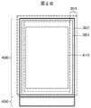
本発明の第1の実施例について、図1〜図4を用いて説明する。図2Aは、本実施例に係る液晶表示装置の概略全体平面図である。本液晶表示装置は表示領域400と駆動回路領域450で構成される。図2Bは、本実施例に係る液晶表示装置におけるメインSOC 302やシールの配置位置を説明するための概略全体平面図である。メインSOCは、液晶表示パネルの周囲を取り巻いて壁状に形成されており、シール301はメインSOCに対してそれぞれの液晶表示パネルの有効表示領域側(以下、内側)に配置される。本実施例では、メインSOC 302の内側に、更にサブSOCを配置した。
A first embodiment of the present invention will be described with reference to FIGS. FIG. 2A is a schematic overall plan view of the liquid crystal display device according to the present embodiment. This liquid crystal display device includes a
図1は本実施例に係る液晶表示装置の要部(シール部)断面図である。本実施例では高さ3μmで、幅0.2mmのメインSOC 302を液晶表示パネルの切断面を含む領域のCF基板側に形成した。これにより、液晶表示パネル毎に切断した後、TFT側基板101とCF側基板201との間の最外周部にはメインSOC 302が配置されるため、有効表示領域410への水分浸入を低減・防止することができる。メインSOC 302は有効表示領域内のSOC 305と同一工程で形成することができる。その際、同じ高さとすることもできるが、有効表示領域内のSOC 305の高さをメインSOC 302の高さよりも低くすることにより、シール盛り上がりによる周辺ギャップ不良を低減・防止することができる。メインSOC 302は有効表示領域内のSOC 305と同様にアクリルやエポキシ等の有機材料で形成することができる。
FIG. 1 is a cross-sectional view of a main part (seal part) of a liquid crystal display device according to this embodiment. In this embodiment, the
また、本実施例ではメインSOC 302の内側に堰き止め用の複数のサブSOC 303を配置した。これにより、万一水分がメインSOC 302を通過した場合でも、サブSOC 303により水分の浸入経路を増大させることができるため、更に信頼性を向上することができる。なお、サブSOC 303の高さをメインSOC 302よりも低くすることにより、液晶表示パネルの切断面付近に塗布されていたシール301が、TFT側基板とCF側基板とを重ね合わせたときにメインSOC 302により押し出された際に内側に流れることを可能とする(シールの逃げが可能)。メインSOC 302とTFT側基板上の配向膜310との間のシールは全て内側に押し出すことが望ましいが、多少残存しても実用上は問題ない。本実施例では、サブSOC 303の高さを2.6μm、幅を7μmとした。また、サブSOC 303はメインSOC 302と同一工程、同一材料で形成した。
In this embodiment, a plurality of
また、本実施例では、TFT側基板の上層パッシベーション膜(UPS)104、又は有機パッシベーション膜(FPS)104に複数の溝を形成し、堰き止めとした。FPS等の厚さは2μmとした。これにより、万一水分がメインSOC 302を通過した場合でも、USP 104、又はFPS 104に形成した溝により水分の浸入経路を増大させることができるため、更に信頼性を向上することができる。更に、サブSOC 303とUSP 104、又はFPS 104に形成した溝とが鉛直上方から見て重なるように配置することにより、配向膜がサブSOCに押されて溝部に入り込もうとするため、その下地膜との密着性を向上することができる。
Further, in this embodiment, a plurality of grooves are formed in the upper layer passivation film (UPS) 104 or the organic passivation film (FPS) 104 of the TFT side substrate to form a dam. The thickness of FPS or the like was 2 μm. As a result, even if moisture passes through the
また、ドレイン配線(DCR)111やゲート配線(GAL)110は、サブSOC 303よりも内側(有効表示領域側)に配置することが望ましい。また、鉛直上方から見て、ドレイン配線(DCR)111やゲート配線(GAL)110は、サブSOC 303と重ならないように配置することが望ましい。ドレイン配線(DCR)111やゲート配線(GAL)110は、切断面から0.2mm程内側に配置した。
Further, it is desirable that the drain wiring (DCR) 111 and the gate wiring (GAL) 110 are arranged on the inner side (effective display area side) than the
次に、本液晶表示装置の製造方法について、図8を参照しながら説明する。先ず、有効表示領域内のSOC 305とサブSOC 306の形成と同一工程で、メインSOC 302とサブSOC 303を形成したCF側基板を準備する。次に、本実施例においては、TFT側基板とCF側基板に、配向膜310を液晶表示パネル毎ではなく、それぞれ複数の液晶表示パネルに渡って形成した。配向膜の厚さは110nmとした。次に、TFT側基板のUSP 104、又はFPS 104に配向膜310を介して溝を形成した。なお、TFT側基板への処理とCF側基板への処理は時系列でなくてもよく、同時並行処理としてもよく、逆にTFT側基板への処理を先行してもよい。次に、CF側基板の切断面を含む領域にシール301を塗布した。シールの幅は0.8mmとした。なお、シールはTFT側基板に塗布することもできる。また、CF側基板とTFT側基板の両者に塗布することもできる。続いて、CF側基板とTFT側基板を、互いに配向膜が形成された面が対向するように重ね合わせ、シールで接着した。各基板を重ね合わせた際、液晶表示パネルの切断面付近に塗布されていたシール301が、TFT側基板とCF側基板とを重ね合わせたときにメインSOC 302により押し出されたシールを内側に流し、各基板間ギャップを調整した。その後、液晶表示パネル毎に切断し、液晶表示装置を完成させた。
Next, a manufacturing method of the present liquid crystal display device will be described with reference to FIG. First, in the same process as the formation of the
なお、液晶表示パネルを切断する前の配置については、図3に示すように駆動回路領域側において、隣接する液晶表示パネルとの間に間隔がある場合(従来の配置)の他、図4に示すように隣接する液晶表示パネルとの間に間隔が無い場合(フルジャスト配置)が考えられる。本実施例によれば、図3に示す配置だけでなく、図4に示すようなフルジャストの配置にも適用することができる。 The arrangement before cutting the liquid crystal display panel is shown in FIG. 4 in addition to the case where there is a space between the adjacent liquid crystal display panels on the drive circuit region side as shown in FIG. 3 (conventional arrangement). As shown, there is a case where there is no space between the adjacent liquid crystal display panels (full just arrangement). According to the present embodiment, the present invention can be applied not only to the arrangement shown in FIG. 3 but also to the full just arrangement as shown in FIG.
図4に示す液晶表示パネルの配置で、図1に示す断面構造の液晶表示装置を、上記製造方法を用いて作製した結果、黒むらの発生はなく、信頼性の高い液晶表示装置を得ることができた。 With the arrangement of the liquid crystal display panel shown in FIG. 4, the liquid crystal display device having the cross-sectional structure shown in FIG. 1 is manufactured using the above manufacturing method, and as a result, a highly reliable liquid crystal display device without black unevenness is obtained. I was able to.
以上、本実施例によれば、液晶表示パネルの切断面を含む領域にメインSOCを設けることにより、狭額縁であっても、信頼性の高い表示装置およびその製造方法を提供することができる。また、メインSOCの内側に複数のサブSOCを配置することにより、より信頼性を向上させることができる。また、メインSOCの内側のUPSやFPSに複数の溝を、配向膜を介して形成することにより、より信頼性を向上させることができる。また、配向膜を複数の液晶表示パネルに渡って印刷することにより、配向膜印刷寸法管理が不要となる。 As described above, according to this embodiment, by providing the main SOC in the region including the cut surface of the liquid crystal display panel, it is possible to provide a highly reliable display device and a method for manufacturing the same even in a narrow frame. Further, by arranging a plurality of sub SOCs inside the main SOC, the reliability can be further improved. Further, by forming a plurality of grooves in the UPS or FPS inside the main SOC via the alignment film, the reliability can be further improved. In addition, by printing the alignment film across a plurality of liquid crystal display panels, the alignment film print size management becomes unnecessary.
本発明の第2の実施例について、図5を用いて説明する。なお、実施例1に記載され本実施例に未記載の事項は特段の事情が無い限り本実施例にも適用することができる。図5は本実施例に係る液晶表示装置の要部(シール部)断面図である。本実施例と実施例1との違いは、実施例1ではTFT側基板101に上層パッシベーション膜(UPS)104、又は有機パッシベーション膜(FPS)104が形成されていたのに対し、本実施例ではこのFPS、又はFPSを有さない点にある。これに伴い、TFT側基板において、配向膜310は無機パッシベーション膜(PAS)上に形成されている。他の構成は実施例1と同様のため説明を省略する。
A second embodiment of the present invention will be described with reference to FIG. Note that the matters described in the first embodiment but not described in the present embodiment can be applied to the present embodiment as long as there is no particular circumstance. FIG. 5 is a cross-sectional view of a main part (seal part) of the liquid crystal display device according to this embodiment. The difference between the present embodiment and the first embodiment is that the upper passivation film (UPS) 104 or the organic passivation film (FPS) 104 is formed on the
本実施例においては、無機パッシベーション膜(PAS)103に複数の溝を形成し、堰き止めとした。これにより、万一水分がメインSOC 302を通過した場合でも、PAS 103に形成した溝により水分の浸入経路を増大させることができるため、更に信頼性を向上することができる。更に、サブSOC 303とPAS 103に形成した溝とが鉛直上方から見て重なるように配置することにより、配向膜がサブSOCに押されて溝部に入り込もうとするため、その下地膜との密着性を向上することができる。
In this example, a plurality of grooves were formed in the inorganic passivation film (PAS) 103 to form a dam. As a result, even if moisture passes through the
次に、本液晶表示装置の製造方法について、図8を参照しながら説明する。なお、TFT側基板にはUPS又はFPSは形成されていない。先ず、有効表示領域内のSOC 305とサブSOC 306の形成と同一工程で、メインSOC 302とサブSOC 303を形成したCF側基板を準備する。次に、本実施例においては、TFT側基板とCF側基板に、配向膜310を液晶表示パネル毎ではなく、それぞれ複数の液晶表示パネルに渡って形成した。配向膜の厚さは110nmとした。次に、TFT基板側のPAS 103に配向膜310を介して溝を形成した。なお、TFT側基板への処理とCF側基板への処理は時系列でなくてもよく、同時並行処理としてもよく、逆にTFT側基板への処理を先行してもよい。次に、CF側基板の切断面を含む領域にシール301を塗布した。シールの幅は0.8mmとした。続いて、CF側基板とTFT側基板を、互いに配向膜が形成された面が対向するように重ね合わせ、シールで接着した。各基板を重ね合わせた際、液晶表示パネルの切断面付近に塗布されていたシール301が、TFT側基板とCF側基板とを重ね合わせたときにメインSOC 302により押し出されたシールを内側に流し、各基板間ギャップを調整した。その後、液晶表示パネル毎に切断し、液晶表示装置を完成させた。
Next, a manufacturing method of the present liquid crystal display device will be described with reference to FIG. Note that no UPS or FPS is formed on the TFT side substrate. First, in the same process as the formation of the
図4に示す液晶表示パネルの配置で、図5に示す断面構造の液晶表示装置を、上記製造方法を用いて作製した結果、黒むらの発生はなく、信頼性の高い液晶表示装置を得ることができた。 As a result of manufacturing the liquid crystal display device having the cross-sectional structure shown in FIG. 5 using the above manufacturing method with the arrangement of the liquid crystal display panel shown in FIG. 4, there is no black unevenness and a highly reliable liquid crystal display device is obtained. I was able to.
以上、本実施例によれば、液晶表示パネルの切断面を含む領域にメインSOCを設けることにより、狭額縁であっても、信頼性の高い表示装置およびその製造方法を提供することができる。また、メインSOCの内側に複数のサブSOCを配置することにより、より信頼性を向上させることができる。また、メインSOCの内側のPASに複数の溝を、配向膜を介して形成することにより、より信頼性を向上させることができる。また、配向膜を複数の液晶表示パネルに渡って印刷することにより、配向膜印刷寸法管理が不要となる。 As described above, according to this embodiment, by providing the main SOC in the region including the cut surface of the liquid crystal display panel, it is possible to provide a highly reliable display device and a method for manufacturing the same even in a narrow frame. Further, by arranging a plurality of sub SOCs inside the main SOC, the reliability can be further improved. Further, the reliability can be further improved by forming a plurality of grooves in the PAS inside the main SOC via the alignment film. In addition, by printing the alignment film across a plurality of liquid crystal display panels, the alignment film print size management becomes unnecessary.
なお、本発明は上記した実施例に限定されるものではなく、様々な変形例が含まれる。例えば、上記した実施例は本発明を分かりやすく説明するために詳細に説明したものであり、必ずしも説明した全ての構成を備えるものに限定されるものではない。また、ある実施例の構成の一部を他の実施例の構成に置き換えることも可能であり、また、ある実施例の構成に他の実施例の構成を加えることも可能である。また、各実施例の構成の一部について、他の構成の追加・削除・置換をすることが可能である。 In addition, this invention is not limited to an above-described Example, Various modifications are included. For example, the above-described embodiments have been described in detail for easy understanding of the present invention, and are not necessarily limited to those having all the configurations described. Further, a part of the configuration of a certain embodiment can be replaced with the configuration of another embodiment, and the configuration of another embodiment can be added to the configuration of a certain embodiment. Further, it is possible to add, delete, and replace other configurations for a part of the configuration of each embodiment.
101…TFT側ガラス基板、102…窒化シリコン膜(ゲート絶縁膜)、103…無機パッシベーション膜(PAS)、104…上層パッシベーション膜(UPS)又は有機パッシベーション膜(FPAS)、110…ゲート配線(GAL)、111…ドレイン配線(DCR)、201…カラーフィルタ(CF)側基板、202…ブラックマトリクス膜(BM)、203…オーバーコート膜(OC)、301…シール、302…メインSOC、303…サブSOC、305…有効表示領域内SOC、306…有効表示領域内サブSOC、310…配向膜、400…表示領域、410…有効表示領域、450…駆動回路領域。
DESCRIPTION OF
Claims (8)
前記第1基板と前記第2基板との端部のギャップには、第1スペーサが壁状に配置され、前記第1スペーサよりも内側に前記シールが配置され、
前記第1基板は、第1無機パッシベーション膜と、前記第1無機パッシベーション膜上に形成された第2無機パッシベーション膜又は有機パッシベーション膜とを有し、
前記第2無機パッシベーション膜又は有機パッシベーション膜は、前記第1配向膜で覆われており、且つ前記シールが形成されている領域内において複数の除去領域を有し、
前記第2基板上であって前記シールの内部に、前記第1スペーサよりも高さの低い第2スペーサが複数配置され、
鉛直上方から見て、前記複数の第2スペーサと前記複数の除去領域とが重なるように配置され、
前記第1基板は前記シールが形成される領域に複数のドレイン配線を有し、
鉛直上方から見て、前記シールが形成される領域のドレイン配線は、隣り合う第2スペーサの間、または、隣り合う除去領域の間に形成されていることを特徴とする表示装置。 A first substrate having a TFT side substrate and a first alignment film formed on the TFT side substrate , and a second substrate having a color filter side substrate and a second alignment film formed on the color filter side substrate And a seal that is in contact with the first alignment film and the second alignment film and bonds the first substrate and the second substrate together,
A first spacer is disposed in the shape of a wall in the gap between the end portions of the first substrate and the second substrate, and the seal is disposed inside the first spacer .
The first substrate includes a first inorganic passivation film, and a second inorganic passivation film or an organic passivation film formed on the first inorganic passivation film,
The second inorganic passivation film or the organic passivation film is covered with the first alignment film, and has a plurality of removal regions in the region where the seal is formed,
A plurality of second spacers having a height lower than that of the first spacer are disposed on the second substrate and inside the seal,
When viewed from vertically above, the plurality of second spacers and the plurality of removal regions are arranged to overlap,
The first substrate has a plurality of drain wirings in a region where the seal is formed,
The display device , wherein the drain wiring in the region where the seal is formed is formed between adjacent second spacers or adjacent removal regions as viewed from above.
前記第1基板と前記第2基板との端部のギャップには、第1スペーサが壁状に配置され、前記第1スペーサよりも内側に前記シールが配置され、
前記第1基板は、前記第1配向膜と前記TFT側基板との間に無機パッシベーション膜を有し、
前記無機パッシベーション膜は、前記シールが形成されている領域内において複数の除去領域を有し、
前記第2基板上であって前記シールの内部に、前記第1スペーサよりも高さの低い第2スペーサが複数配置され、
鉛直上方から見て、前記複数の第2スペーサと前記複数の除去領域とが重なるように配置され、
前記第1基板は前記シールが形成される領域に複数のドレイン配線を有し、
鉛直上方から見て、前記シールが形成される領域のドレイン配線は、隣り合う第2スペーサの間、または、隣り合う除去領域の間に形成されていることを特徴とする表示装置。 A first substrate having a TFT side substrate and a first alignment film formed on the TFT side substrate, and a second substrate having a color filter side substrate and a second alignment film formed on the color filter side substrate And a seal that is in contact with the first alignment film and the second alignment film and bonds the first substrate and the second substrate together ,
A first spacer is disposed in the shape of a wall in the gap between the end portions of the first substrate and the second substrate, and the seal is disposed inside the first spacer.
The first substrate has an inorganic passivation film between the first alignment film and the TFT side substrate,
The inorganic passivation film has a plurality of removal regions in the region where the seal is formed,
A plurality of second spacers having a height lower than that of the first spacer are disposed on the second substrate and inside the seal ,
When viewed from vertically above, the plurality of second spacers and the plurality of removal regions are arranged to overlap,
The first substrate has a plurality of drain wirings in a region where the seal is formed,
The display device , wherein the drain wiring in the region where the seal is formed is formed between adjacent second spacers or adjacent removal regions as viewed from above.
前記表示装置は、前記第1基板と前記第2基板とのギャップ距離調整用のスペーサを備えた有効表示領域を有し、
前記第1スペーサの高さは、前記有効表示領域のスペーサの高さよりも高いことを特徴とする表示装置。 The display device according to claim 1 or 2 ,
The display device has an effective display area including a spacer for adjusting a gap distance between the first substrate and the second substrate,
The display device according to claim 1, wherein a height of the first spacer is higher than a height of the spacer in the effective display area .
前記第1スペーサと前記有効表示領域のスペーサとは同じ材料で形成されていることを特徴とする表示装置。 The display device according to claim 3 ,
The display device, wherein the first spacer and the spacer in the effective display region are formed of the same material .
前記第1基板上の複数の前記表示パネル領域に渡って第1配向膜を形成する工程と、
それぞれ有効表示領域を備えた複数の表示パネル領域を有し、前記表示パネル領域の切断面を含む領域にギャップ距離調整用の第1スペーサが形成された第2基板を準備する工程と、
前記第2基板上の複数の前記表示パネル領域に渡って第2配向膜を形成する工程と、
前記第2基板の前記第1スペーサが形成された領域、及び/又は前記第1基板の前記表示パネル領域の切断面を含む領域の前記第1配向膜若しくは前記第2配向膜にシールを塗布する工程と、
前記第1基板の前記第1配向膜と前記第2基板の前記第2配向膜とが互いに対向するように、前記第1基板と前記第2基板とを重ね合わせ、前記シールにより互いに接着する工程と、
前記第1スペーサが分断されるように、前記切断面で前記表示パネル領域を切断する工程と、を有し、
前記第1基板は、無機パッシベーション膜と、前記無機パッシベーション膜上に形成された上層パッシベーション膜又は有機パッシベーション膜とを有し、
前記上層パッシベーション膜又は有機パッシベーション膜は、前記第1配向膜で覆われており、且つ前記シールが形成される領域内において複数の除去領域を有し、
前記第2基板上であって前記シールの内部となる位置に、前記第1スペーサよりも高さの低い第2スペーサが複数配置され、
鉛直上方から見て、前記複数の第2スペーサと前記複数の除去領域とが重なるように前記第1基板と前記第2基板とを重ね合わせるとともに、
前記第1基板は前記シールが形成される領域に複数のドレイン配線を有し、
鉛直上方から見て、前記複数のドレイン配線が前記複数の第2スペーサ及び前記複数の除去領域とは重ならないように、前記第1基板と前記第2基板とを重ね合わせることを特徴とする表示装置の製造方法。 Preparing a first substrate having a plurality of display panel regions each having an effective display region;
Forming a first alignment film over the plurality of display panel regions on the first substrate;
Providing a second substrate having a plurality of display panel regions each having an effective display region, and having a first spacer for adjusting a gap distance formed in a region including a cut surface of the display panel region;
Forming a second alignment film over the plurality of display panel regions on the second substrate;
A seal is applied to the first alignment film or the second alignment film in a region of the second substrate where the first spacer is formed and / or a region including a cut surface of the display panel region of the first substrate. Process,
The first substrate and the second substrate are stacked so that the first alignment film of the first substrate and the second alignment film of the second substrate face each other, and are bonded to each other by the seal When,
Cutting the display panel region at the cut surface so that the first spacer is divided,
The first substrate includes an inorganic passivation film, and an upper passivation film or an organic passivation film formed on the inorganic passivation film,
The upper passivation film or the organic passivation film is covered with the first alignment film, and has a plurality of removal regions in a region where the seal is formed,
A plurality of second spacers having a height lower than that of the first spacer are disposed on the second substrate at a position inside the seal,
As seen from vertically above, the first substrate and the second substrate are overlaid so that the plurality of second spacers and the plurality of removal regions overlap,
Wherein the first substrate includes a plurality of drain wiring in a region where the seal is formed,
When viewed from vertically above, the as plurality of drain lines do not overlap with the plurality of second spacers and the plurality of removed areas, the display characterized by superposing the first substrate and the second substrate Device manufacturing method .
前記第1基板上の複数の前記表示パネル領域に渡って第1配向膜を形成する工程と、
それぞれ有効表示領域を備えた複数の表示パネル領域を有し、前記表示パネル領域の切断面を含む領域にギャップ距離調整用の第1スペーサが形成された第2基板を準備する工程と、
前記第2基板上の複数の前記表示パネル領域に渡って第2配向膜を形成する工程と、
前記第2基板の前記第1スペーサが形成された領域、及び/又は前記第1基板の前記表示パネル領域の切断面を含む領域の前記第1配向膜若しくは前記第2配向膜にシールを塗布する工程と、
前記第1基板の前記第1配向膜と前記第2基板の前記第2配向膜とが互いに対向するように、前記第1基板と前記第2基板とを重ね合わせ、前記シールにより互いに接着する工程と、
前記第1スペーサが分断されるように、前記切断面で前記表示パネル領域を切断する工程と、を有し、
前記第1基板は、TFT側基板と、前記TFT側基板と前記第1配向膜との間に形成された無機パッシベーション膜とを有し、
前記無機パッシベーション膜は、前記シールが形成される領域内において複数の除去領域を有し、
前記第2基板上であって前記シールの内部に、前記第1スペーサよりも高さの低い第2スペーサが複数配置され、
鉛直上方から見て、前記複数の第2スペーサと前記複数の除去領域とが重なるように前記第1基板と前記第2基板とを重ね合わせ、
前記第1基板は前記シールが形成される領域に複数のドレイン配線を有し、
鉛直上方から見て、前記複数のドレイン配線が前記複数の第2スペーサ及び前記複数の除去領域とは重ならないように、前記第1基板と前記第2基板とを重ね合わせることを特徴とする表示装置の製造方法。 Preparing a first substrate having a plurality of display panel regions each having an effective display region;
Forming a first alignment film over the plurality of display panel regions on the first substrate;
Providing a second substrate having a plurality of display panel regions each having an effective display region, and having a first spacer for adjusting a gap distance formed in a region including a cut surface of the display panel region;
Forming a second alignment film over the plurality of display panel regions on the second substrate;
A seal is applied to the first alignment film or the second alignment film in a region of the second substrate where the first spacer is formed and / or a region including a cut surface of the display panel region of the first substrate. Process,
The first substrate and the second substrate are stacked so that the first alignment film of the first substrate and the second alignment film of the second substrate face each other, and are bonded to each other by the seal When,
Cutting the display panel region at the cut surface so that the first spacer is divided,
The first substrate includes a TFT-side substrate, and an inorganic passivation film which is formed between the first alignment film and the TFT side substrate,
The inorganic passivation film is to have a plurality of removal area in the area where the seal is formed,
A plurality of second spacers having a height lower than that of the first spacer are disposed on the second substrate and inside the seal,
When viewed from vertically above, the first substrate and the second substrate are overlapped so that the plurality of second spacers and the plurality of removal regions overlap,
The first substrate has a plurality of drain wirings in a region where the seal is formed ,
When viewed from vertically above, the as plurality of drain lines do not overlap with the plurality of second spacers and the plurality of removed areas, and wherein the Rukoto superposing the first substrate and the second substrate Manufacturing method of display device.
前記表示パネルは、前記第1基板と前記第2基板とのギャップ距離調整用のスペーサを備えた有効表示領域を有し、
前記第1スペーサの高さは、前記有効表示領域のスペーサの高さよりも高いことを特徴とする表示装置の製造方法。 It is a manufacturing method of the display device according to claim 5 or 6 ,
The display panel has an effective display area including a spacer for adjusting a gap distance between the first substrate and the second substrate,
The method of manufacturing a display device , wherein the height of the first spacer is higher than the height of the spacer in the effective display area .
前記第1スペーサと前記有効表示領域のスペーサとは同じ工程で形成されることを特徴とする表示装置の製造方法。 It is a manufacturing method of the display device according to claim 7,
Manufacturing method of the display device and the spacer of the effective display region and the first spacer, wherein Rukoto formed in the same step.
Priority Applications (12)
| Application Number | Priority Date | Filing Date | Title |
|---|---|---|---|
| JP2012219420A JP6192914B2 (en) | 2012-10-01 | 2012-10-01 | Display device and manufacturing method thereof |
| US14/034,827 US9104073B2 (en) | 2012-10-01 | 2013-09-24 | Display device and manufacturing method thereof |
| US14/791,122 US9395585B2 (en) | 2012-10-01 | 2015-07-02 | Display device and manufacturing method thereof |
| US15/189,106 US10007152B2 (en) | 2012-10-01 | 2016-06-22 | Display device and manufacturing method thereof |
| US15/988,107 US10162221B2 (en) | 2012-10-01 | 2018-05-24 | Display device and manufacturing method thereof |
| US16/197,449 US10503025B2 (en) | 2012-10-01 | 2018-11-21 | Display device and manufacturing method thereof |
| US16/679,407 US10712622B2 (en) | 2012-10-01 | 2019-11-11 | Display device and manufacturing method thereof |
| US16/893,620 US10996526B2 (en) | 2012-10-01 | 2020-06-05 | Display device and manufacturing method thereof |
| US17/223,100 US11333940B2 (en) | 2012-10-01 | 2021-04-06 | Display device and manufacturing method thereof |
| US17/718,457 US11573464B2 (en) | 2012-10-01 | 2022-04-12 | Display device and manufacturing method thereof |
| US18/089,629 US11852932B2 (en) | 2012-10-01 | 2022-12-28 | Display device and manufacturing method thereof |
| US18/387,510 US20240069392A1 (en) | 2012-10-01 | 2023-11-07 | Display device and manufacturing method thereof |
Applications Claiming Priority (1)
| Application Number | Priority Date | Filing Date | Title |
|---|---|---|---|
| JP2012219420A JP6192914B2 (en) | 2012-10-01 | 2012-10-01 | Display device and manufacturing method thereof |
Publications (3)
| Publication Number | Publication Date |
|---|---|
| JP2014071410A JP2014071410A (en) | 2014-04-21 |
| JP2014071410A5 JP2014071410A5 (en) | 2015-11-12 |
| JP6192914B2 true JP6192914B2 (en) | 2017-09-06 |
Family
ID=50384852
Family Applications (1)
| Application Number | Title | Priority Date | Filing Date |
|---|---|---|---|
| JP2012219420A Active JP6192914B2 (en) | 2012-10-01 | 2012-10-01 | Display device and manufacturing method thereof |
Country Status (2)
| Country | Link |
|---|---|
| US (11) | US9104073B2 (en) |
| JP (1) | JP6192914B2 (en) |
Families Citing this family (23)
| Publication number | Priority date | Publication date | Assignee | Title |
|---|---|---|---|---|
| JP2010139953A (en) | 2008-12-15 | 2010-06-24 | Hitachi Displays Ltd | Liquid crystal display device |
| JP6192914B2 (en) * | 2012-10-01 | 2017-09-06 | 株式会社ジャパンディスプレイ | Display device and manufacturing method thereof |
| CN103676330B (en) * | 2013-12-23 | 2017-02-01 | 合肥京东方光电科技有限公司 | Array substrate and display device |
| JP6348297B2 (en) * | 2014-02-21 | 2018-06-27 | 株式会社ジャパンディスプレイ | Display device |
| CN103995385B (en) * | 2014-05-09 | 2017-12-05 | 京东方科技集团股份有限公司 | Display master blank and its cutting method |
| JP6502638B2 (en) * | 2014-09-10 | 2019-04-17 | 株式会社ジャパンディスプレイ | Liquid crystal display device and mother substrate |
| US20160170247A1 (en) * | 2014-12-12 | 2016-06-16 | Apple Inc. | Display with Spacer Ring |
| JP6440486B2 (en) * | 2014-12-19 | 2018-12-19 | 株式会社ジャパンディスプレイ | LCD panel |
| CN104765180B (en) * | 2015-04-30 | 2018-06-15 | 京东方科技集团股份有限公司 | A kind of display master blank, display panel, display device |
| JP6608201B2 (en) | 2015-07-10 | 2019-11-20 | 株式会社ジャパンディスプレイ | Self-luminous display device |
| CN105204212B (en) * | 2015-11-05 | 2018-07-10 | 京东方科技集团股份有限公司 | Display base plate, display panel cutting method and display device |
| CN105467689A (en) * | 2016-01-04 | 2016-04-06 | 武汉华星光电技术有限公司 | Liquid crystal panel to be cut off and method for cutting off liquid crystal panel |
| US10690970B2 (en) * | 2016-04-08 | 2020-06-23 | Apple Inc. | Display with hybrid column spacer structures |
| JP2018017978A (en) * | 2016-07-29 | 2018-02-01 | 株式会社ジャパンディスプレイ | Display device |
| JP2018017988A (en) * | 2016-07-29 | 2018-02-01 | 株式会社ジャパンディスプレイ | Display device |
| CN106249466A (en) * | 2016-10-11 | 2016-12-21 | 京东方科技集团股份有限公司 | Display master blank and cutting method thereof |
| CN109782474B (en) * | 2018-01-29 | 2022-04-12 | 友达光电(昆山)有限公司 | Display panel |
| JP7030578B2 (en) * | 2018-03-16 | 2022-03-07 | 株式会社ジャパンディスプレイ | Display device |
| CN109633960B (en) * | 2019-01-29 | 2021-08-24 | 惠州市华星光电技术有限公司 | Liquid crystal display module and liquid crystal display device |
| CN109870854A (en) * | 2019-03-28 | 2019-06-11 | 武汉华星光电技术有限公司 | Display panel and display device |
| CN110687723A (en) * | 2019-09-11 | 2020-01-14 | 深圳市华星光电技术有限公司 | Light emitting panel and display device |
| CN111208682B (en) * | 2020-01-19 | 2021-04-27 | Tcl华星光电技术有限公司 | Liquid crystal display panel and display device |
| CN113514985B (en) * | 2021-05-25 | 2022-10-21 | 上海中航光电子有限公司 | Display panel and display device |
Family Cites Families (22)
| Publication number | Priority date | Publication date | Assignee | Title |
|---|---|---|---|---|
| CN1179237C (en) * | 1998-08-31 | 2004-12-08 | 精工爱普生株式会社 | Liquid crystal panel and method of manufacture thereof |
| JP2001235749A (en) * | 2000-02-21 | 2001-08-31 | Seiko Epson Corp | Method for manufacturing electrooptical device, electrooptical device and projection type display device |
| JP4609679B2 (en) * | 2000-07-19 | 2011-01-12 | 日本電気株式会社 | Liquid crystal display |
| KR100865284B1 (en) * | 2001-10-31 | 2008-10-27 | 엘지디스플레이 주식회사 | A sealing structure of liquid crsytal panel |
| KR100972148B1 (en) * | 2002-12-31 | 2010-07-23 | 엘지디스플레이 주식회사 | a liquid crystal display device featuring a layered structure under a seal pattern |
| JP2006030440A (en) * | 2004-07-14 | 2006-02-02 | Seiko Epson Corp | Manufacturing method of liquid crystal device, liquid crystal device and electronic device |
| KR101107693B1 (en) * | 2004-11-24 | 2012-01-25 | 엘지디스플레이 주식회사 | Liquid Crystal Display Device |
| JP2007248743A (en) * | 2006-03-15 | 2007-09-27 | Seiko Epson Corp | Liquid crystal device and its manufacturing method, and electronic equipment |
| JP2007304452A (en) | 2006-05-15 | 2007-11-22 | Hitachi Displays Ltd | Liquid crystal display device |
| JP4869892B2 (en) * | 2006-12-06 | 2012-02-08 | 株式会社 日立ディスプレイズ | Liquid crystal display |
| JP2007148449A (en) | 2007-03-08 | 2007-06-14 | Sharp Corp | Liquid crystal display device |
| JP2009122410A (en) * | 2007-11-15 | 2009-06-04 | Seiko Epson Corp | Electrooptical device |
| JP2010091896A (en) * | 2008-10-10 | 2010-04-22 | Hitachi Displays Ltd | Liquid crystal display device |
| KR101603315B1 (en) * | 2009-09-25 | 2016-03-15 | 삼성디스플레이 주식회사 | Liquid crystal display and manufacturing method thereof |
| KR101403739B1 (en) * | 2010-04-16 | 2014-06-03 | 샤프 가부시키가이샤 | Display device |
| JP5457321B2 (en) * | 2010-09-28 | 2014-04-02 | 株式会社ジャパンディスプレイ | Liquid crystal display |
| KR101719484B1 (en) * | 2010-10-04 | 2017-03-27 | 삼성디스플레이 주식회사 | Display substrate and display device comprising the same |
| JP5299873B2 (en) | 2010-11-30 | 2013-09-25 | 株式会社ジャパンディスプレイ | LCD panel |
| KR20130000938A (en) * | 2011-06-24 | 2013-01-03 | 삼성디스플레이 주식회사 | Liquid crystal display device and method of manufacturing a liquid crystal display device |
| JP5897984B2 (en) * | 2011-07-08 | 2016-04-06 | 株式会社ジャパンディスプレイ | Display device |
| JP5637629B2 (en) | 2011-07-22 | 2014-12-10 | 株式会社ジャパンディスプレイ | Display device |
| JP6192914B2 (en) * | 2012-10-01 | 2017-09-06 | 株式会社ジャパンディスプレイ | Display device and manufacturing method thereof |
-
2012
- 2012-10-01 JP JP2012219420A patent/JP6192914B2/en active Active
-
2013
- 2013-09-24 US US14/034,827 patent/US9104073B2/en active Active
-
2015
- 2015-07-02 US US14/791,122 patent/US9395585B2/en active Active
-
2016
- 2016-06-22 US US15/189,106 patent/US10007152B2/en active Active
-
2018
- 2018-05-24 US US15/988,107 patent/US10162221B2/en active Active
- 2018-11-21 US US16/197,449 patent/US10503025B2/en active Active
-
2019
- 2019-11-11 US US16/679,407 patent/US10712622B2/en active Active
-
2020
- 2020-06-05 US US16/893,620 patent/US10996526B2/en active Active
-
2021
- 2021-04-06 US US17/223,100 patent/US11333940B2/en active Active
-
2022
- 2022-04-12 US US17/718,457 patent/US11573464B2/en active Active
- 2022-12-28 US US18/089,629 patent/US11852932B2/en active Active
-
2023
- 2023-11-07 US US18/387,510 patent/US20240069392A1/en active Pending
Also Published As
| Publication number | Publication date |
|---|---|
| US11573464B2 (en) | 2023-02-07 |
| US20160306206A1 (en) | 2016-10-20 |
| JP2014071410A (en) | 2014-04-21 |
| US10162221B2 (en) | 2018-12-25 |
| US10712622B2 (en) | 2020-07-14 |
| US20240069392A1 (en) | 2024-02-29 |
| US20220236602A1 (en) | 2022-07-28 |
| US10503025B2 (en) | 2019-12-10 |
| US10007152B2 (en) | 2018-06-26 |
| US20200073166A1 (en) | 2020-03-05 |
| US10996526B2 (en) | 2021-05-04 |
| US9104073B2 (en) | 2015-08-11 |
| US20200301191A1 (en) | 2020-09-24 |
| US20230138640A1 (en) | 2023-05-04 |
| US20190086700A1 (en) | 2019-03-21 |
| US11852932B2 (en) | 2023-12-26 |
| US20150309349A1 (en) | 2015-10-29 |
| US11333940B2 (en) | 2022-05-17 |
| US20180267348A1 (en) | 2018-09-20 |
| US9395585B2 (en) | 2016-07-19 |
| US20140092351A1 (en) | 2014-04-03 |
| US20210223599A1 (en) | 2021-07-22 |
Similar Documents
| Publication | Publication Date | Title |
|---|---|---|
| JP6192914B2 (en) | Display device and manufacturing method thereof | |
| JP5261300B2 (en) | Liquid crystal display | |
| JP2008309863A (en) | Method for manufacturing liquid crystal display panel, and liquid crystal display panel | |
| US8755017B2 (en) | Electronic apparatus, liquid crystal display and manufacturing method thereof | |
| JP5266736B2 (en) | Liquid crystal display element and manufacturing method thereof | |
| JP2011145441A (en) | Method for manufacturing liquid crystal display, liquid crystal display, and electronic equipment | |
| US20170329190A1 (en) | Array substrate and manufacturing method for the same, and display device | |
| JP2015036712A (en) | Manufacturing method of liquid crystal display panel | |
| US20160282677A1 (en) | Method for manufacturing liquid crystal display panel, and liquid crystal display panel | |
| KR101386751B1 (en) | Liquid crystal display device | |
| JP6035081B2 (en) | Liquid crystal display | |
| JP2009093066A (en) | Liquid crystal display device | |
| JP2024006210A (en) | Liquid crystal display panel, electronic device, and manufacturing method for liquid crystal display panel | |
| JP5903742B2 (en) | Mother color filter substrate | |
| JP5026883B2 (en) | Electro-optical device and electronic apparatus | |
| JP2011128188A (en) | Liquid crystal display device and method of manufacturing the same | |
| JP2012073443A (en) | Mother substrate, and method for manufacturing liquid crystal panel manufactured by using the mother substrate | |
| JP2009093036A (en) | Display panel | |
| JP2011180549A (en) | Liquid crystal display device, method of manufacturing the same, and electronic apparatus | |
| KR20070040565A (en) | Method of manufacturing liquid crystal display device | |
| JP2013167902A (en) | Manufacturing method of liquid crystal display device | |
| KR20120127298A (en) | Electronic device, liquid crystal display and manufacturing the same | |
| JP2007171317A (en) | Liquid crystal display panel, manufacturing method therefor and electronic equipment | |
| JP2006126755A (en) | Liquid crystal display and its manufacturing method |
Legal Events
| Date | Code | Title | Description |
|---|---|---|---|
| A521 | Request for written amendment filed |
Free format text: JAPANESE INTERMEDIATE CODE: A523 Effective date: 20150924 |
|
| A621 | Written request for application examination |
Free format text: JAPANESE INTERMEDIATE CODE: A621 Effective date: 20150924 |
|
| A977 | Report on retrieval |
Free format text: JAPANESE INTERMEDIATE CODE: A971007 Effective date: 20160518 |
|
| A131 | Notification of reasons for refusal |
Free format text: JAPANESE INTERMEDIATE CODE: A131 Effective date: 20160531 |
|
| A521 | Request for written amendment filed |
Free format text: JAPANESE INTERMEDIATE CODE: A523 Effective date: 20160725 |
|
| A131 | Notification of reasons for refusal |
Free format text: JAPANESE INTERMEDIATE CODE: A131 Effective date: 20161220 |
|
| A521 | Request for written amendment filed |
Free format text: JAPANESE INTERMEDIATE CODE: A523 Effective date: 20170214 |
|
| TRDD | Decision of grant or rejection written | ||
| A01 | Written decision to grant a patent or to grant a registration (utility model) |
Free format text: JAPANESE INTERMEDIATE CODE: A01 Effective date: 20170711 |
|
| A61 | First payment of annual fees (during grant procedure) |
Free format text: JAPANESE INTERMEDIATE CODE: A61 Effective date: 20170809 |
|
| R150 | Certificate of patent or registration of utility model |
Ref document number: 6192914 Country of ref document: JP Free format text: JAPANESE INTERMEDIATE CODE: R150 |
|
| R250 | Receipt of annual fees |
Free format text: JAPANESE INTERMEDIATE CODE: R250 |
|
| R250 | Receipt of annual fees |
Free format text: JAPANESE INTERMEDIATE CODE: R250 |
|
| R250 | Receipt of annual fees |
Free format text: JAPANESE INTERMEDIATE CODE: R250 |
|
| R250 | Receipt of annual fees |
Free format text: JAPANESE INTERMEDIATE CODE: R250 |