JP2013167902A - Manufacturing method of liquid crystal display device - Google Patents
Manufacturing method of liquid crystal display device Download PDFInfo
- Publication number
- JP2013167902A JP2013167902A JP2013093149A JP2013093149A JP2013167902A JP 2013167902 A JP2013167902 A JP 2013167902A JP 2013093149 A JP2013093149 A JP 2013093149A JP 2013093149 A JP2013093149 A JP 2013093149A JP 2013167902 A JP2013167902 A JP 2013167902A
- Authority
- JP
- Japan
- Prior art keywords
- film
- seal portion
- alignment
- substrate
- color filter
- Prior art date
- Legal status (The legal status is an assumption and is not a legal conclusion. Google has not performed a legal analysis and makes no representation as to the accuracy of the status listed.)
- Granted
Links
- 239000004973 liquid crystal related substance Substances 0.000 title claims abstract description 76
- 238000004519 manufacturing process Methods 0.000 title claims description 11
- 239000000758 substrate Substances 0.000 claims abstract description 163
- 239000003566 sealing material Substances 0.000 claims description 37
- 238000000034 method Methods 0.000 claims description 26
- 239000000463 material Substances 0.000 claims description 22
- 230000001678 irradiating effect Effects 0.000 claims description 6
- 238000010030 laminating Methods 0.000 claims description 6
- 239000003086 colorant Substances 0.000 claims 4
- 230000009467 reduction Effects 0.000 abstract description 3
- 230000000149 penetrating effect Effects 0.000 abstract description 2
- 230000005855 radiation Effects 0.000 abstract 3
- 230000015556 catabolic process Effects 0.000 abstract 1
- 238000006731 degradation reaction Methods 0.000 abstract 1
- 230000003287 optical effect Effects 0.000 abstract 1
- 239000010408 film Substances 0.000 description 325
- 239000010410 layer Substances 0.000 description 25
- 238000002161 passivation Methods 0.000 description 14
- 230000008569 process Effects 0.000 description 11
- 230000007423 decrease Effects 0.000 description 8
- 239000011229 interlayer Substances 0.000 description 7
- 239000011159 matrix material Substances 0.000 description 7
- 238000005498 polishing Methods 0.000 description 7
- 239000000853 adhesive Substances 0.000 description 6
- 230000001070 adhesive effect Effects 0.000 description 6
- 239000000956 alloy Substances 0.000 description 5
- 229910045601 alloy Inorganic materials 0.000 description 5
- 229910021417 amorphous silicon Inorganic materials 0.000 description 5
- 239000007788 liquid Substances 0.000 description 5
- 230000002093 peripheral effect Effects 0.000 description 5
- OAICVXFJPJFONN-UHFFFAOYSA-N Phosphorus Chemical compound [P] OAICVXFJPJFONN-UHFFFAOYSA-N 0.000 description 4
- 230000015572 biosynthetic process Effects 0.000 description 4
- 210000002858 crystal cell Anatomy 0.000 description 4
- 239000011521 glass Substances 0.000 description 4
- 230000007480 spreading Effects 0.000 description 4
- 229910015202 MoCr Inorganic materials 0.000 description 3
- 229920000642 polymer Polymers 0.000 description 3
- 238000007789 sealing Methods 0.000 description 3
- 239000004065 semiconductor Substances 0.000 description 3
- 238000009751 slip forming Methods 0.000 description 3
- 238000004544 sputter deposition Methods 0.000 description 3
- 238000002834 transmittance Methods 0.000 description 3
- XLYOFNOQVPJJNP-UHFFFAOYSA-N water Substances O XLYOFNOQVPJJNP-UHFFFAOYSA-N 0.000 description 3
- 230000005540 biological transmission Effects 0.000 description 2
- 239000011248 coating agent Substances 0.000 description 2
- 238000000576 coating method Methods 0.000 description 2
- 230000001276 controlling effect Effects 0.000 description 2
- 230000000694 effects Effects 0.000 description 2
- 230000005684 electric field Effects 0.000 description 2
- 230000012447 hatching Effects 0.000 description 2
- 239000012466 permeate Substances 0.000 description 2
- 238000000206 photolithography Methods 0.000 description 2
- 239000000047 product Substances 0.000 description 2
- 230000001105 regulatory effect Effects 0.000 description 2
- 125000006850 spacer group Chemical group 0.000 description 2
- 239000000126 substance Substances 0.000 description 2
- 230000009471 action Effects 0.000 description 1
- 230000000903 blocking effect Effects 0.000 description 1
- 210000004027 cell Anatomy 0.000 description 1
- 230000002950 deficient Effects 0.000 description 1
- 230000005611 electricity Effects 0.000 description 1
- 238000005530 etching Methods 0.000 description 1
- 238000007687 exposure technique Methods 0.000 description 1
- 239000003365 glass fiber Substances 0.000 description 1
- 239000012535 impurity Substances 0.000 description 1
- AMGQUBHHOARCQH-UHFFFAOYSA-N indium;oxotin Chemical compound [In].[Sn]=O AMGQUBHHOARCQH-UHFFFAOYSA-N 0.000 description 1
- 230000004048 modification Effects 0.000 description 1
- 238000012986 modification Methods 0.000 description 1
- 238000000059 patterning Methods 0.000 description 1
- 230000035515 penetration Effects 0.000 description 1
- 238000005268 plasma chemical vapour deposition Methods 0.000 description 1
- 230000010287 polarization Effects 0.000 description 1
- 230000001681 protective effect Effects 0.000 description 1
- 239000007787 solid Substances 0.000 description 1
- 230000003068 static effect Effects 0.000 description 1
- 239000010409 thin film Substances 0.000 description 1
Images


Abstract
Description
本発明は表示装置に係り、特に、シール部の信頼性を改善した、IPS方式の液晶表示装置に関する。 The present invention relates to a display device, and more particularly to an IPS liquid crystal display device in which the reliability of a seal portion is improved.
液晶表示装置では画素電極および薄膜トランジスタ(TFT)等がマトリクス状に形成されたTFT基板と、TFT基板に対向して、TFT基板の画素電極と対応する場所にカラーフィルタ等が形成された対向基板が設置され、TFT基板と対向基板の間に液晶が挟持されている。そして液晶分子による光の透過率を画素毎に制御することによって画像を形成している。 In a liquid crystal display device, there are a TFT substrate in which pixel electrodes and thin film transistors (TFTs) are formed in a matrix, and a counter substrate in which color filters are formed at locations corresponding to the pixel electrodes of the TFT substrate, facing the TFT substrate. The liquid crystal is sandwiched between the TFT substrate and the counter substrate. An image is formed by controlling the light transmittance of the liquid crystal molecules for each pixel.
液晶表示装置はフラットで軽量であることから、TV等の大型表示装置から、携帯電話やDSC(Digital Still Camera)等の小型の表示装置まで、色々な分野で用途が広がっている。一方、液晶表示装置では視野角特性が問題である。視野角特性は、画面を正面から見た場合と、斜め方向から見た場合に、輝度が変化したり、色度が変化したりする現象である。視野角特性は、液晶分子を水平方向の電界によって動作させるIPS(In Plane Switching)方式が優れた特性を有している。 Since the liquid crystal display device is flat and lightweight, its application is expanding in various fields from a large display device such as a TV to a small display device such as a mobile phone and a DSC (Digital Still Camera). On the other hand, viewing angle characteristics are a problem in liquid crystal display devices. The viewing angle characteristic is a phenomenon in which luminance changes or chromaticity changes when the screen is viewed from the front and when viewed from an oblique direction. The viewing angle characteristic is excellent in an IPS (In Plane Switching) system in which liquid crystal molecules are operated by a horizontal electric field.
IPS方式では、配向膜付近の液晶分子に対してプレティルト角を形成する必要がない。このため、配向膜に対する配向軸の形成を、ラビング方式によらず、光配向方式によって行うことが出来る。光配向は、ラビング方式に比べて、静電気の発生が無い等の利点を有している。 In the IPS system, it is not necessary to form a pretilt angle for the liquid crystal molecules in the vicinity of the alignment film. For this reason, the alignment axis can be formed on the alignment film by the photo-alignment method, not by the rubbing method. The photo-alignment has advantages such as no generation of static electricity compared to the rubbing method.
光配向は、配向膜に偏光した紫外線を照射することによって、配向膜に対し所定の方向に液晶分子を配向させるような異方性をもたせるものである。このような光配向に関する技術を記載したものとして、「特許文献1」が挙げられる。
In the photo-alignment, the alignment film is irradiated with polarized ultraviolet rays so that the alignment film has anisotropy to align liquid crystal molecules in a predetermined direction. “
光配向は、ポリマーで形成された配向膜に対して特定の方向に偏光した紫外線を照射することによって行われる。例えば、網目状に形成されたポリマーに対して、偏光した紫外線を照射すると、紫外線の偏光方向に対する特定の方向のポリマーが破壊される。これによって、配向膜に液晶分子を配向させるための異方性を形成することが出来る。光配向させる偏光紫外線が配向膜のみに照射されるのであれば、問題は無いが、配向膜以外の部分に照射されると、照射された部分が紫外線によって劣化し、問題を生ずる。 Photo-alignment is performed by irradiating an alignment film formed of a polymer with ultraviolet rays polarized in a specific direction. For example, when a polymer formed in a network is irradiated with polarized ultraviolet rays, the polymer in a specific direction with respect to the polarization direction of the ultraviolet rays is destroyed. Thereby, anisotropy for aligning liquid crystal molecules in the alignment film can be formed. There is no problem if the polarized ultraviolet light to be photo-aligned is irradiated only to the alignment film, but if the portion other than the alignment film is irradiated, the irradiated portion deteriorates due to the ultraviolet light, causing a problem.
IPS方式の液晶表示装置は、小型の液晶表示装置についても使用されている。小型の液晶表示装置は、1個ずつ製作したのでは、効率が悪いので、マザー基板に多数の液晶表示装置を形成し、多数の液晶表示装置を同時に製造することが行われる。 IPS liquid crystal display devices are also used for small liquid crystal display devices. If small liquid crystal display devices are manufactured one by one, the efficiency is poor. Therefore, a large number of liquid crystal display devices are formed on a mother substrate, and a large number of liquid crystal display devices are manufactured simultaneously.
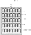
図13は、マザー基板に35枚の小型の液晶表示セル1が作られている例である。TFTや画素電極を有するTFT基板100が多数形成されたマザーTFT基板1000とカラーフィルタ等が形成された対向基板200が多数形成されたマザー対向基板2000を貼り合わせる。マザーTFT基板1000とマザー対向基板2000はシール材15およびマザー基板シール材151で接着される。図13において、シール材15で囲まれた斜線を施した長方形は配向膜113が形成される範囲を示している。
FIG. 13 shows an example in which 35 small liquid
小型の液晶表示装置は薄いことが要求されており、例えば、TFT基板および対向基板の板厚は0.2mm程度の薄さになる。しかし、このような薄いガラスは規格品としては存在しない。また、このような薄いガラス基板を工程内に通すことは現状では不可能である。したがって、マザー対向基板2000あるいはマザーTFT基板1000の状態では、板厚が0.5mm程度の厚さのガラスを用い、マザー対向基板2000とマザーTFT基板1000を貼り合わせてマザー基板にした後、マザー対向基板2000あるいはマザーTFT基板1000の外側を研磨する。
Small liquid crystal display devices are required to be thin. For example, the thicknesses of the TFT substrate and the counter substrate are as thin as about 0.2 mm. However, such a thin glass does not exist as a standard product. In addition, it is impossible to pass such a thin glass substrate through the process. Therefore, in the state of the
研磨は機械研磨と化学研磨を併用して行われることが多い。機械研磨にせよ化学研磨にせよ、研磨剤がマザー基板の内部に侵入すると、内部の液晶セル1が不良になるので、マザー基板シール材151によってマザー基板の内部を保護する。マザー基板周辺に形成されたマザー基板シール材151は、マザー基板封止材161によって封止される。図13に示すマザー基板は、研磨後、各液晶セルに分離される。
図14は図13に示すマザー基板を構成するマザー対向基板2000の状態を示したものであり、図13の液晶セル1に対応して対向基板200が35枚形成されている。図14は、マザー対向基板2000にシール材15あるいはマザー基板シール材151を形成する前の段階である。図14において、配向膜113が各対向基板200毎に形成されている。シール部に配向膜が存在すると、シール材15の接着力が低下するので、配向膜113は、シール部を避けて、かつ表示領域を覆うように形成される。
Polishing is often performed using both mechanical polishing and chemical polishing. Whether the polishing is mechanical polishing or chemical polishing, if the abrasive enters the inside of the mother substrate, the
FIG. 14 shows a state of the
図14において、配向膜113は、フレキソ印刷によって形成される。配向膜113を形成した後、偏光紫外線を使用して配向膜113に対して光配向を行う。このときの偏光紫外線の照射は、マザー対向基板2000全面に対して行う。個々の配向膜毎に偏光紫外線を照射すると製造コストが上昇するからである。したがって、配向膜が形成されていない部分にも偏光紫外線が照射されることになる。
In FIG. 14, the
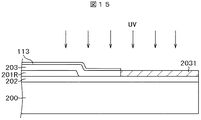
図15は、個々の対向基板200の端部における断面構造であり、光配向のための偏光紫外線が照射されている状態を示している。対向基板200の端部には、後で説明するように、遮光膜202、カラーフィルタ201、オーバーコート膜203等が形成されている。遮光膜202は画面のコントラストを向上させたり、画面周辺の見栄えをよくさせたりする役割を有し、ブラックマトリクスとも呼ばれているが、本明細書では遮光膜という用語を用いる。図15に示すように、配向膜113が存在していない部分では、オーバーコート膜203の斜線で示す部分2031に紫外線が直接照射されるために、この部分のオーバーコート膜2031が劣化し、オーバーコート膜203が容易に水分を通すようになる。
FIG. 15 is a cross-sectional structure at the end portion of each
図16は、偏光紫外線によって光配向を行った後、シール材15を形成した状態を示す対向基板200の端部断面図である。オーバーコート膜203の斜線で示した部分2031は紫外線によって劣化しているために、この部分のオーバーコート膜2031を通して水分が遮光膜202の表面に浸透する。
FIG. 16 is an end cross-sectional view of the
図17は、TFT基板100と対向基板200を接着し、内部に液晶300を封入した状態の液晶表示パネルの端部の断面図である。図17において、TFT基板100には、無機パッシベーション膜106、有機パッシベーション膜107、および、配向膜113が形成されている。また、対向基板200には、遮光膜202、カラーフィルタ201、オーバーコート膜203、および、配向膜113が形成されている。図17において、対向基板200におけるオーバーコート膜203のうち、斜線で示した部分2031は、光配向時の、紫外線によって劣化しているので、この部分において、外部から水分が容易に浸入する。
FIG. 17 is a cross-sectional view of the end portion of the liquid crystal display panel in a state where the
劣化したオーバーコート膜2031から水分が浸入すると、この水分は遮光膜202に達し、遮光膜202を変質させる。特に、遮光膜202に水分が作用すると、遮光膜202と基板200との接着力が低下し、シール部における信頼性が低下する。また、遮光膜202に水分が作用すると、遮光膜202の電気抵抗が低下し、遮光膜202の影響によって液晶層300における電界が乱れ、光漏れによってコントラストが低下する。
When moisture enters from the deteriorated
本発明の課題は、光配向時に紫外線照射によって劣化したオーバーコート膜に起因して外部から浸入する水分が、遮光膜へ影響を及ぼすことを防止することである。 An object of the present invention is to prevent moisture entering from the outside due to an overcoat film deteriorated by ultraviolet irradiation during photo-alignment from affecting the light shielding film.
本発明は、以上のような課題を解決するものであり、具体的な構成は次のとおりである。 The present invention solves the above-described problems, and a specific configuration is as follows.
(1)TFTおよび画素電極を有する画素がマトリクス状に形成された表示領域を有するTFT基板と、遮光膜と3色のカラーフィルタが形成され、3色のカラーフィルタを覆ってオーバーコート膜が形成され、前記オーバーコート膜を覆って配向膜が形成された表示領域を有する対向基板が周辺のシール部においてシール材によって接着し、前記TFT基板と前記対向基板の間に液晶が封入された液晶表示装置であって、前記対向基板において、前記配向膜は光配向によって配向処理が施され、前記配向膜は前記シール部には形成されておらず。前記対向基板の前記シール部には、遮光膜と前記3色のカラーフィルタのうちの一色のカラーフィルタとオーバーコート膜がこの順で積層して形成され、前記オーバーコート膜の上に前記シール材が形成されていることを特徴とする液晶表示装置。 (1) A TFT substrate having a display area in which pixels having TFTs and pixel electrodes are formed in a matrix, a light shielding film and three color filters are formed, and an overcoat film is formed to cover the three color filters A liquid crystal display in which a counter substrate having a display region in which an alignment film is formed so as to cover the overcoat film is bonded by a sealing material at a peripheral seal portion, and liquid crystal is sealed between the TFT substrate and the counter substrate In the counter substrate, the alignment film is subjected to an alignment process by photo-alignment, and the alignment film is not formed on the seal portion. A light shielding film, one color filter of the three color filters, and an overcoat film are laminated in this order on the seal portion of the counter substrate, and the seal material is formed on the overcoat film. A liquid crystal display device, wherein:
(2)TFTおよび画素電極を有する画素がマトリクス状に形成された表示領域を有するTFT基板と、遮光膜と3色のカラーフィルタが形成され、3色のカラーフィルタを覆ってオーバーコート膜が形成され、前記オーバーコート膜を覆って配向膜が形成された表示領域を有する対向基板が周辺のシール部においてシール材によって接着し、前記TFT基板と前記対向基板の間に液晶が封入された液晶表示装置であって、前記対向基板において、前記配向膜は光配向によって配向処理が施され、前記配向膜は前記シール部には形成されておらず。前記対向基板の前記シール部には、遮光膜と前記3色のカラーフィルタのうちの複数の色のカラーフィルタが積層して形成され、前記積層されたカラーフィルタを覆ってオーバーコート膜が形成され、前記オーバーコート膜の上に前記シール材が形成されていることを特徴とする液晶表示装置。 (2) A TFT substrate having a display area in which pixels having TFTs and pixel electrodes are formed in a matrix, a light shielding film and three color filters are formed, and an overcoat film is formed to cover the three color filters A liquid crystal display in which a counter substrate having a display region in which an alignment film is formed so as to cover the overcoat film is bonded by a sealing material at a peripheral seal portion, and liquid crystal is sealed between the TFT substrate and the counter substrate In the counter substrate, the alignment film is subjected to an alignment process by photo-alignment, and the alignment film is not formed on the seal portion. The seal portion of the counter substrate is formed by laminating a light shielding film and a plurality of color filters of the three color filters, and an overcoat film is formed covering the laminated color filters. A liquid crystal display device, wherein the sealing material is formed on the overcoat film.
(3)前記シール部に形成された複数のカラーフィルタのうちのひとつは前記表示領域に形成されたカラーフィルタと連続して形成され、前記複数のカラーフィルタのうちの他のカラーフィルタは前記表示領域に形成されたカラーフィルタとは連続していないことを特徴とする(2)に記載の液晶表示装置。 (3) One of the plurality of color filters formed on the seal portion is formed continuously with the color filter formed on the display area, and the other color filter of the plurality of color filters is the display. The liquid crystal display device according to (2), wherein the color filter formed in the region is not continuous.
(4)TFTおよび画素電極を有する画素がマトリクス状に形成された表示領域を有するTFT基板と、遮光膜と3色のカラーフィルタが形成され、3色のカラーフィルタを覆ってオーバーコート膜が形成され、前記オーバーコート膜を覆って配向膜が形成された表示領域を有する対向基板が周辺のシール部においてシール材によって接着し、前記TFT基板と前記対向基板の間に液晶が封入された液晶表示装置であって、前記対向基板において、前記配向膜は光配向によって配向処理が施され、前記配向膜は前記シール部には形成されておらず。前記対向基板の前記シール部には、遮光膜と前記3色のカラーフィルタのうちの一色のカラーフィルタとオーバーコート膜がこの順で積層して形成され、前記シール部に形成された前記一色のカラーフィルタは、前記表示領域に形成された3色のカラーフィルタのいずれとも連続して形成されておらず、前記シール部に形成された一色のカラーフィルタの端部に対応して、前記オーバーコート膜には段差が形成されており、前記オーバーコート膜の上に前記シール材が形成されていることを特徴とする液晶表示装置。 (4) A TFT substrate having a display area in which pixels having TFTs and pixel electrodes are formed in a matrix, a light shielding film and three color filters are formed, and an overcoat film is formed covering the three color filters. A liquid crystal display in which a counter substrate having a display region in which an alignment film is formed so as to cover the overcoat film is bonded by a sealing material at a peripheral seal portion, and liquid crystal is sealed between the TFT substrate and the counter substrate In the counter substrate, the alignment film is subjected to an alignment process by photo-alignment, and the alignment film is not formed on the seal portion. On the seal portion of the counter substrate, a light-shielding film, one color filter of the three color filters, and an overcoat film are laminated in this order, and the one color of the one color formed on the seal portion is formed. The color filter is not formed continuously with any of the three color filters formed in the display area, and corresponds to the end of the one color filter formed on the seal portion. The liquid crystal display device is characterized in that a step is formed on the film, and the sealing material is formed on the overcoat film.
(5)TFTおよび画素電極を有する画素がマトリクス状に形成された表示領域を有するTFT基板と、遮光膜と3色のカラーフィルタが形成され、3色のカラーフィルタを覆ってオーバーコート膜が形成され、前記オーバーコート膜を覆って配向膜が形成された表示領域を有する対向基板が周辺のシール部においてシール材によって接着し、前記TFT基板と前記対向基板の間に液晶が封入された液晶表示装置であって、前記対向基板において、前記配向膜は光配向によって配向処理が施され、前記配向膜は前記シール部には形成されておらず。前記対向基板の前記シール部には、遮光膜と前記3色のカラーフィルタのうちの複数の色のカラーフィルタが積層して形成され、前記積層されたカラーフィルタを覆ってオーバーコート膜が形成され、前記シール部に形成された前記複数のカラーフィルタは、前記表示領域に形成された3色のカラーフィルタのいずれとも連続して形成されておらず、前記シール部に形成された複数のカラーフィルタの端部に対応して、前記オーバーコート膜には段差が形成されており、前記オーバーコート膜の上に前記シール材が形成されていることを特徴とする液晶表示装置。 (5) A TFT substrate having a display region in which pixels having TFTs and pixel electrodes are formed in a matrix, a light shielding film and three color filters are formed, and an overcoat film is formed to cover the three color filters A liquid crystal display in which a counter substrate having a display region in which an alignment film is formed so as to cover the overcoat film is bonded by a sealing material at a peripheral seal portion, and liquid crystal is sealed between the TFT substrate and the counter substrate In the counter substrate, the alignment film is subjected to an alignment process by photo-alignment, and the alignment film is not formed on the seal portion. The seal portion of the counter substrate is formed by laminating a light shielding film and a plurality of color filters of the three color filters, and an overcoat film is formed covering the laminated color filters. The plurality of color filters formed in the seal portion are not continuously formed with any of the three color filters formed in the display area, and the plurality of color filters formed in the seal portion. A step is formed in the overcoat film corresponding to the end of the liquid crystal display device, and the sealing material is formed on the overcoat film.
(6)TFTおよび画素電極を有する画素がマトリクス状に形成された表示領域を有するTFT基板と、遮光膜と3色のカラーフィルタが形成され、3色のカラーフィルタを覆ってオーバーコート膜が形成され、前記オーバーコート膜を覆って配向膜が形成された表示領域を有する対向基板が周辺のシール部においてシール材によって接着し、前記TFT基板と前記対向基板の間に液晶が封入された液晶表示装置であって、前記対向基板において、前記配向膜は光配向によって配向処理が施され、前記配向膜は前記シール部には形成されておらず。前記対向基板の前記シール部には、遮光膜とオーバーコート膜がこの順で積層して形成され、前記シール部における前記オーバーコート膜の厚さは前記表示領域におけるオーバーコート膜の膜厚よりも大きく、前記オーバーコート膜の上に前記シール材が形成されていることを特徴とする液晶表示装置。 (6) A TFT substrate having a display area in which pixels having TFTs and pixel electrodes are formed in a matrix, a light shielding film and three color filters are formed, and an overcoat film is formed to cover the three color filters A liquid crystal display in which a counter substrate having a display region in which an alignment film is formed so as to cover the overcoat film is bonded by a sealing material at a peripheral seal portion, and liquid crystal is sealed between the TFT substrate and the counter substrate In the counter substrate, the alignment film is subjected to an alignment process by photo-alignment, and the alignment film is not formed on the seal portion. A light shielding film and an overcoat film are laminated in this order on the seal portion of the counter substrate, and the thickness of the overcoat film in the seal portion is larger than the film thickness of the overcoat film in the display region. A liquid crystal display device characterized in that the sealing material is formed on the overcoat film.
(7)前記シール部における前記オーバーコート膜の膜厚は、前記表示領域における前記オーバーコート膜の膜厚の1.5倍以上であることを特徴とする(6)に記載の液晶表示装置。 (7) The liquid crystal display device according to (6), wherein a film thickness of the overcoat film in the seal portion is 1.5 times or more of a film thickness of the overcoat film in the display region.
本発明によれば、光配向において、紫外線によってシール部のオーバーコート膜が劣化しても、オーバーコート膜の下にカラーフィルタを配置することによって、水分が劣化したオーバーコート膜に透過してきても、水分がカラーフィルタによってブロックされ、遮光膜に到達しにくくなるので、遮光膜の剥がれを防止することが出来る。また、遮光膜の電気抵抗が低下することを防止することが出来るので、液晶層の光漏れによるコントラストの低下を防止することが出来る。 According to the present invention, in the photo-alignment, even if the overcoat film of the seal portion deteriorates due to the ultraviolet rays, even if the color filter is disposed under the overcoat film, the moisture can permeate the overcoat film. Since moisture is blocked by the color filter and hardly reaches the light shielding film, peeling of the light shielding film can be prevented. In addition, since it is possible to prevent the electric resistance of the light shielding film from being lowered, it is possible to prevent a reduction in contrast due to light leakage of the liquid crystal layer.
また、本発明の別な態様によれば、シール部のオーバーコート膜を表示領域のオーバーコート膜よりも厚く形成するので、オーバーコート膜全体が光配向時の紫外線によって劣化することを防止することによって、水分が遮光膜に到達することを防止することが出来る。また、表示領域のオーバーコート膜の膜厚は厚くしないので、表示画面の輝度の低下は防止することが出来る。 According to another aspect of the present invention, since the overcoat film of the seal portion is formed thicker than the overcoat film of the display area, the entire overcoat film is prevented from being deteriorated by ultraviolet rays during photo-alignment. Therefore, it is possible to prevent moisture from reaching the light shielding film. In addition, since the thickness of the overcoat film in the display area is not increased, a reduction in the luminance of the display screen can be prevented.
以下、実施例によって本発明の内容を詳細に説明する。 Hereinafter, the contents of the present invention will be described in detail by way of examples.
図1は、本発明が適用される製品の例である、携帯電話等に使用される小型の液晶表示装置の平面図である。図1において、TFT基板100上に対向基板200が設置されている。TFT基板100と対向基板200の間に液晶層が挟持されている。TFT基板100と対向基板200とは額縁部に形成されたシール材15によって接着している。図1においてシール材15には封入孔が形成され、封入孔から液晶が封入される。その後封入孔は封止材16によって封止される。
FIG. 1 is a plan view of a small liquid crystal display device used in a mobile phone or the like, which is an example of a product to which the present invention is applied. In FIG. 1, a
TFT基板100は対向基板200よりも大きく形成されており、TFT基板100が対向基板200よりも大きくなっている部分には、液晶表示パネルに電源、映像信号、走査信号等を供給するための端子部150が形成されている。また、端子部150には、走査線、映像信号線等を駆動するためのICドライバ50が設置されている。ICドライバ50は3つの領域に分かれており、中央には映像信号駆動回路52が設置され、両脇には走査信号駆動回路51が設置されている。
The
図1の表示領域10において、横方向には走査線30が延在し、縦方向に配列している。また、縦方向には映像信号線40が延在し、横方向に配列している。走査線30は走査線引出し線31によって、ICドライバ50の走査信号駆動回路51と接続している。図1において、表示領域10を液晶表示装置の中央に配置するために、走査線引出し線31は表示領域10の両側に配置され、このために、ICドライバ50には、走査信号駆動回路51が両脇に設置されている。一方映像信号線40とICドライバ50を接続する映像信号線引出し線41は画面下側に集められている。映像信号線引出し線41はICドライバ50の中央部に配置されている映像信号駆動回路52と接続する。
In the display area 10 of FIG. 1,
図1の表示領域10よりも若干広い領域に配向膜113が形成されている。この配向膜113には光配向がなされている。シール材15が形成された部分には配向膜113は形成されていない。配向膜が113存在すると、シール材113と基板との接着力が低下するからである。
An
図2はIPS方式の液晶表示装置の表示領域における構造を示す断面図である。IPS方式の液晶表示装置の電極構造は種々のものが提案され、実用化されている。図1の構造は、現在広く使用されている構造であって、簡単に言えば、平面ベタで形成された対向電極108の上に層間絶縁膜109を挟んで櫛歯状の画素電極110が形成されている。そして、画素電極110と対向電極108の間の電圧によって液晶分子301を回転させることによって画素毎に液晶層300の光の透過率を制御することにより画像を形成するものである。以下に図1の構造を詳しく説明する。なお、本発明は、図1の構成を例にとって説明するが、図2以外のIPSタイプの液晶表示装置にも適用することが出来る。
FIG. 2 is a cross-sectional view showing a structure in a display region of an IPS liquid crystal display device. Various electrode structures of IPS liquid crystal display devices have been proposed and put into practical use. The structure shown in FIG. 1 is a structure that is widely used at present. To put it simply, a comb-
図2において、ガラスで形成されるTFT基板100の上に、ゲート電極101が形成されている。ゲート電極101は走査線と同層で形成されている。ゲート電極101はAlNd合金の上にMoCr合金が積層されている。
In FIG. 2, a
ゲート電極101を覆ってゲート絶縁膜102がSiNによって形成されている。ゲート絶縁膜102の上に、ゲート電極101と対向する位置に半導体層103がa−Si膜によって形成されている。a−Si膜はプラズマCVDによって形成される。a−Si膜はTFTのチャネル部を形成するが、チャネル部を挟んでa−Si膜上にソース電極104とドレイン電極105が形成される。なお、a−Si膜とソース電極104あるいはドレイン電極105との間には図示しないn+Si層が形成される。半導体層とソース電極104あるいはドレイン電極105とのオーミックコンタクトを取るためである。
A
ソース電極104は映像信号線が兼用し、ドレイン電極105は画素電極110と接続される。ソース電極104もドレイン電極105も同層で同時に形成される。本実施例では、ソース電極104あるいはドレイン電極105はMoCr合金で形成される。ソース電極104あるいはドレイン電極105の電気抵抗を下げたい場合等は、例えば、AlNd合金をMoCr合金でサンドイッチした電極構造が用いられる。
The
TFTを覆って無機パッシベーション膜106がSiNによって形成される。無機パッシベーション膜106はTFTの、特にチャネル部を不純物401から保護する。無機パッシベーション膜106の上には有機パッシベーション膜107が形成される。有機パッシベーション膜107はTFTの保護と同時に表面を平坦化する役割も有するので、厚く形成される。厚さは1μmから4μmである。
An
有機パッシベーション膜107の上には対向電極108が形成される。対向電極108は透明導電膜であるITO(Indium Tin Oxide)を表示領域全体にスパッタリングすることによって形成される。すなわち、対向電極108は面状に形成される。対向電極108を全面にスパッタリングによって形成した後、画素電極110とドレイン電極105を導通するためのスルーホール111部だけは対向電極108をエッチングによって除去する。
A
対向電極108を覆って層間絶縁膜109がSiNによって形成される。層間絶縁膜109が形成された後、スルーホール111を形成する。その後、層間絶縁膜109およびスルーホール111を覆って画素電極110となるITOを被着形成する。被着したITOをパターニングして画素電極110を形成する。画素電極110となるITOはスルーホール111にも被着される。スルーホール111において、TFTから延在してきたドレイン電極105と画素電極110が導通し、映像信号が画素電極110に供給されることになる。
An interlayer insulating
画素電極はいわゆる櫛歯状の電極となっている。櫛歯状の電極と櫛歯状の電極の間は図2に示すスリット112となっている。対向電極108には一定電圧が印加され、画素電極110には映像信号による電圧が印加される。画素電極110に電圧が印加されると図1に示すように、電気力線が発生して液晶分子301を電気力線の方向に回転させてバックライトからの光の透過を制御する。画素毎にバックライトからの透過が制御されるので、画像が形成されることになる。なお、画素電極110の上には液晶分子301を配向させるためのTFT基板側配向膜113が形成されている。配向膜に対する配向処理は偏光紫外線による光配向が用いられる。
The pixel electrode is a so-called comb-like electrode. A
図2の例では、有機パッシベーション膜107の上に、面状に形成された対向電極108が配置され、層間絶縁膜109の上に櫛歯電極110が配置されている。しかしこれとは逆に、有機パッシベーション膜107の上に面状に形成された画素電極110を配置し、層間絶縁膜109の上に櫛歯状の対向電極108が配置される場合もある。
In the example of FIG. 2, a
図2において、液晶層300を挟んで対向基板200が設置されている。対向基板200の内側には、カラーフィルタが形成されている。図2においては、赤カラーフィルタ201Rが形成されている。カラーフィルタの下の、画像を形成しない領域には遮光膜202が形成されている。遮光膜202は、画像のコントラストを向上させるとともに、TFTの遮光膜としての役割を有し、TFTに光電流が流れることを防止している。
In FIG. 2, the
カラーフィルタ201および遮光膜202を覆ってオーバーコート膜203が形成されている。カラーフィルタ201および遮光膜202の表面は凹凸となっているために、オーバーコート膜203によって表面を平らにしている。オーバーコート膜203の上には、液晶の初期配向を決めるための配向膜113が形成されている。配向膜113は光配向処理されている。
An
図2はIPSであるから、対向電極108はTFT基板100側に形成されており、対向基板200側には形成されていない。このように、IPSでは、対向基板200の内側には導電膜が形成されていない。そうすると、対向基板200の電位が不安定になる。また、外部からの電磁ノイズが液晶層300に侵入し、画像に対して影響を与える。このような問題を除去するために、対向基板200の外側に表面導電膜210が形成される。表面導電膜210は、透明導電膜であるITOをスパッタリングすることによって形成される。
Since FIG. 2 shows IPS, the
図3は図1に示す液晶表示装置の端部における断面図である。図3において、TFT基板100には無機パッシベーション膜106と有機パッシベーション膜107と配向膜113が形成されている。TFT基板100のその他の構成は図3では省略している。対向基板200には、遮光膜202、赤カラーフィルタ201R、オーバーコート膜203、配向膜113が形成されている。端部はシール材15によってシールされ、TFT基板100と対向基板200の間隔はグラスファイバによるスペーサー350によって規定されている。
FIG. 3 is a cross-sectional view at the end of the liquid crystal display device shown in FIG. In FIG. 3, an
図3において、配向膜113は光配向によって配向処理されている。図3に示す本発明の特徴は、端部において、オーバーコート膜203の下に赤カラーフィルタ201Rを配置していることとである。図3では赤カラーフィルタ210Rが形成されているが、緑カラーフィルタでも青カラーフィルタでも良い。図3の対向基板200において、配向膜113が存在していない部分のオーバーコート膜203は、光配向時の紫外線によって劣化し、水分が浸入し易い状態となっている。
In FIG. 3, the
オーバーコート膜203が紫外線によって劣化していても、オーバーコート膜203の下には赤カラーフィルタ201Rが存在している。したがって、オーバーコート膜203に進入して来た水分は、赤カラーフィルタ201Rによってブロックされ、下層の遮光膜202に到達しないか、到達までに長時間かかる。したがって、遮光膜202が水分と反応することによる接着力の低下、あるいは、遮光膜202の電気抵抗の低下は防止することが出来る。
Even if the
図4および図5は以上の説明を図に示すものである。図4は対向基板200に遮光膜202、赤カラーフィルタ201R、オーバーコート膜203、配向膜113がこの順で形成された状態を示している。遮光膜202の膜厚は1μm程度、赤カラーフィルタ201Rの膜厚は1〜2μm、オーバーコート膜203の膜厚は1〜2μm、配向膜113の膜厚は0.1μm程度である。緑カラーフィルタ、青カラーフィルタ等の膜厚も1〜2μmである。
4 and 5 illustrate the above description. FIG. 4 shows a state in which the
配向膜113は、端部には形成されていない。配向膜113によってシール材15の接着力が低下することを防止するためである。図4において、配向膜113に配向処理するために、紫外線UVを照射する。配向膜113は、紫外線によって配向処理をうけるが、配向膜113が存在しない、端部における、斜線を施したオーバーコート膜2031は紫外線によって劣化する。
The
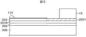
その後、図5に示すように、配向膜113が存在していない、端部におけるオ−バーコート膜203の上にシール材15が形成される。図5において、紫外線によって劣化したオーバーコート膜の斜線で示す部分2031には水分が容易に浸透する。しかし、斜線で示したオーバーコート膜2031の下には赤カラーフィルタ201Rが存在しているので、侵入した水分は赤カラーフィルタ201Rによってブロックされ、遮光膜202には容易に到達しない。したがって、シール部の信頼性を確保することが出来る。
Thereafter, as shown in FIG. 5, the sealing
従来は、カラーフィルタは表示領域のみに形成されていたが、本発明では、これを対向基板200の端部にまで延在させている。カラーフィルタはフォトリソグラフィによって形成される。つまり、カラーフィルタの形成範囲は露光マスクによって規定することが出来る。したがって、カラーフィルタを対向基板の端部にまで形成するとしても、工程が増加することは無い。
Conventionally, the color filter is formed only in the display region, but in the present invention, this is extended to the end of the
このように、本実施例によれば、光配向処理においてオーバーコート膜203が紫外線によって劣化しても、オーバーコート膜203を浸透して来た水分の影響をカラーフィルタがブロックするので、シール部の信頼性が低下することは無い。また、水分が遮光膜202と反応することによる遮光膜202の電気抵抗の低下も防止することが出来るので、液晶の光漏れに起因するコントラストの低下を防止することが出来る。
As described above, according to the present embodiment, even if the
以上の実施例においては、シール部に形成されるカラーフィルタは赤カラーフィルタ201Rであるとしているが、これは、例であって、他のカラーフィルタ、すなわち、緑カラーフィルタであっても青カラーフィルタであっても良い。
In the above embodiment, the color filter formed in the seal portion is the
図6は、本発明の第2の実施例による対向基板200の端部付近における断面図である。図6において、対向基板200には、遮光膜202、赤カラーフィルタ201R、オーバーコート膜203、配向膜113がこの順で形成されている。ただし、配向膜113が存在しないシール部には、赤カラーフィルタ201Rと緑カラーフィルタ201Gが積層して形成されている。配向膜113は光配向処理される。したがって、配向膜113が存在していない部分のオーバーコート膜203は紫外線によって劣化する。
FIG. 6 is a cross-sectional view in the vicinity of the end of the
図6においては、紫外線によって劣化したオーバーコート膜203の下には、緑カラーフィルタ201Gと赤カラーフィルタ201Rの2層のカラーフィルタが形成されている。したがって、たとえ、劣化したオーバーコート膜203に水分は浸透してきても、浸透してきた水分は、緑カラーフィルタ201Gおよび赤カラーフィルタ201Rによってブロックされ、遮光膜202に到達しない。
In FIG. 6, two layers of color filters, a
図6の構成は、シール部においてカラーフィルタが2層形成されているので、実施例1の構成よりも水分に対する防御効果は大きい。各層の膜厚は、実施例1と同様である。つまり、緑カラーフィルタも赤カラーフィルタも実施例1と同様に1〜2μmの厚さに形成される。 6 has two layers of color filters in the seal portion, and therefore has a greater protective effect against moisture than the configuration of the first embodiment. The film thickness of each layer is the same as in Example 1. That is, both the green color filter and the red color filter are formed to a thickness of 1 to 2 μm as in the first embodiment.
図6の構成における別の効果は、配向膜113を塗布したとき、配向膜113がシール部に侵入することを防止することが出来る点である。図6に示すように、端部付近において、緑カラーフィルタ201Gが形成されているので、オーバーコート膜203に段差が生じ、この段差が表示領域から流れてきた配向膜203に対するストッパーとしての役割を持つ。
Another effect of the configuration of FIG. 6 is that the
配向膜203は、塗布されるときは、液体であるので、流動性をもっており、塗布面積を正確に規定することは困難である。特に配向膜113がシール材15の下に存在すると、シール材15の接着力を低下させる。本実施例では、図6に示すように、緑蛍光体201Gによって段差を形成することによって配向膜113の範囲を規定することができるので、シール部における信頼性を高く保つことが出来る。なお、周辺に形成する緑カラーフィルタ201Gはフォトリソグラフィによって形成するので、正確な寸法を維持することが出来る。また、段差の高さは、緑カラーフィルタの厚さである1〜2μm程度である。
Since the
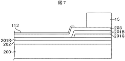
図7は本実施例における他の態様である。図7の左側の表示領域は図6で説明したのと同様であるが、端部は図6とは異なり、遮光膜202とオーバーコート膜203との間には、順番に赤カラーフィルタ201R、緑カラーフィルタ201G、青カラーフィルタ201Bの3層のカラーフィルタが形成されている。配向膜113が光配向処理を受けることは実施例1あるいは図6と同様である。
FIG. 7 shows another aspect of this embodiment. The display area on the left side of FIG. 7 is the same as that described with reference to FIG. 6, but the end portion is different from FIG. 6, and the red color filter 201 </ b> R is sequentially placed between the
図7において、配向膜113に覆われていない部分のオーバーコート膜203が光配向時の紫外線によって劣化することは実施例1と同様である。本実施例では劣化したオーバーコート膜203に浸透して来た水分が遮光膜202に達するまでには3層のカラーフィルタが存在しているので、図6の場合よりも、さらにシール部の信頼性を向上させることが出来る。
In FIG. 7, the portion of the
また、図7に示すように、シール部付近には、緑カラーフィルタ201G、青カラーフィルタ201Bの2層のカラーフィルタによって段差が形成されているので、この段差によって配向膜113の形成範囲を規定することが出来る。本実施例では、2層のカラーフィルタによって段差を形成しおり、段差の大きさは、2μmから4μm程度に形成することが出来るので、配向膜の塗布範囲をより確実に規定することが出来る。
Further, as shown in FIG. 7, a step is formed in the vicinity of the seal portion by the two color filters of the
本実施例では、図6においては、赤カラーフィルタ201Rと緑カラーフィルタ201Gが順に積層されているが、2層のカラーフィルタはこれに限らず、他のカラーフィルタでもよいし、積層する順番も異なっていても良い。また、図7においては、積層するカラーフィルタの順番は、赤カラーフィルタ201R、緑カラーフィルタ201G、青カラーフィルタ201Bの順番であるが、カラーフィルタの積層の順番はこれに限らず、カラーフィルタの製造条件によって任意に決めることが出来る。
In this embodiment, in FIG. 6, the
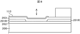
図8は実施例3の対向基板200の端部付近の断面図である。図8において、対向基板200の上には、遮光膜202、赤カラーフィルタ201R、オーバーコート膜203、配向膜113がこの順で形成されている。配向膜113は光配向処理されている。したがって、光配向時に、配向膜113に覆われていない部分のオーバーコート膜203が紫外線によって劣化する。
FIG. 8 is a cross-sectional view of the vicinity of the end portion of the
紫外線によって劣化したオーバーコート膜203と遮光膜202の間に赤カラーフィルタ201Rを配置することによって、劣化したオーバーコート膜203に浸透して来た水分を赤蛍光体201Rによってブロックすることは、実施例1と同様である。本実施例では、実施例1とは異なり、赤カラーフィルタ201Rを端部まで連続して形成するのではなく、表示領域とシール部との間に赤蛍光体を除去した領域、すなわち、図8におけるA部を設ける。
By disposing the
A部の存在によって、赤カラーフィルタ1層のみをシール部に形成する場合も配向膜113に対する段差を形成して、この段差を配向膜の広がりに対するストッパーとして使用することが出来る。また、A部は、配向膜113に対する、いわば液溜りとして作用し、配向膜113の外側への広がりを、段差とともに、より確実に防止することが出来る。
Even when only one red color filter layer is formed in the seal portion due to the presence of the A portion, a step with respect to the
本実施例においては、シール部に形成されるカラーフィルタは赤カラーフィルタ210Rであるとしているが、これは、例であって、他のカラーフィルタ、すなわち、緑カラーフィルタ201Gであっても青カラーフィルタ201Bであっても良い。
In the present embodiment, the color filter formed in the seal portion is the red color filter 210R. However, this is an example, and other color filters, that is, the
図9は実施例4の対向基板200の端部付近の断面図である。図9において、対向基板200の上には、遮光膜202、赤カラーフィルタ201R、オーバーコート膜203、配向膜113がこの順で形成されている。但し、シール部においてはオーバーコート膜203と遮光膜202の間に赤カラーフィルタ201Rと緑カラーフィルタ201Gが存在している。配向膜113は光配向処理されている。したがって、光配向時に、配向膜113に覆われていない部分のオーバーコート膜203が紫外線によって劣化する。
FIG. 9 is a cross-sectional view of the vicinity of the end portion of the
紫外線によって劣化したオーバーコート膜203と遮光膜の間に赤カラーフィルタ201Rおよび緑カラーフィルタ201Gを配置することによって、劣化したオーバーコート膜203に浸透して来た水分をブロックすることは、実施例2における図6と同様である。本実施例では、図6とは異なり、赤カラーフィルタ201Rを端部まで連続して形成するのではなく、表示領域とシール部との間に赤カラーフィルタ201Rを除去した領域、図8におけるA部を設ける。
The arrangement of the
A部の存在によって、シール部付近に形成される段差は赤カラーフィルタ201Rと緑カラーフィルタ201Gの2層分となり、段差の大きさは2μmから4μmとすることが出来る。したがって、外側へ広がろうとする配向膜113をより効果的に規制することが出来る。また、A部は、配向膜113に対する、いわば液溜りとして作用し、配向膜113の外側への広がりを、段差とともに、より確実に防止することが出来る。
Due to the presence of the A portion, the step formed in the vicinity of the seal portion becomes two layers of the
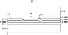
図10は実施例4の、他の態様を示す、対向基板200の端部付近の断面図である。図10は、シール部において、オーバーコート膜203と遮光膜202の間に、赤カラーフィルタ201R、緑カラーフィルタ201G、青カラーフィルタ201Bの3層のカラーフィルタが存在している他は図9と同様である。
FIG. 10 is a cross-sectional view of the vicinity of the end portion of the
図10の構成において、光配向時の紫外線によって劣化したオーバーコート膜203と遮光膜202の間に赤カラーフィルタ201R、緑カラーフィルタ201Gおよび青カラーフィルタ201Bを配置することによって、劣化したオーバーコート膜203に浸透して来た水分をブロックすることは実施例2の図7と同様である。但し、本実施例では、図7とは異なり、赤カラーフィルタ201Rを端部まで連続して形成するのではなく、表示領域とシール部との間に赤蛍光体201Rを除去した領域、図8におけるA部を設ける。
In the configuration of FIG. 10, the red overcoat film 203R, the
A部の存在によって、シール部付近に形成される段差は赤カラーフィルタ201R、緑カラーフィルタ201Gおよび青カラーフィルタ201Bの3層分となり、外側へ広がろうとする配向膜113をより効果的に規制することが出来る。3層分の段差であるから、段差は3μmから6μm程度とすることが出来、配向膜113の粘度が小さい場合であっても、ストッパーとして役割を十分に果たすことが出来る。また、A部は、配向膜113に対する、いわば液溜りとして作用し、配向膜113の外側への広がりを、段差とともに、より確実に防止することが出来る。
Due to the presence of the A portion, the step formed in the vicinity of the seal portion is equivalent to three layers of the
このように、本実施例では、実施例3の場合よりも、劣化したオーバーコート膜203に浸透して来た水分の影響をより確実に防止できる。また、配向膜113の外形の規定も本実施例の構成によれば、より確実に行うことができる。
Thus, in the present embodiment, the influence of moisture that has permeated into the deteriorated
本実施例では、図9においては、赤カラーフィルタ201Rと緑カラーフィルタ201Gが順に積層されているが、2層のカラーフィルタはこれに限らず、他のカラーフィルタでもよいし、積層する順番も異なっていても良い。また、図10においては、積層するカラーフィルタの順番は、赤カラーフィルタ、緑カラーフィルタ、青カラーフィルタの順番であるが、カラーフィルタの積層の順番はこれに限らず、カラーフィルタの製造条件によって任意に決めることが出来る。
In the present embodiment, the
図11は、本発明の第5の実施例を示す対向基板200の端部付近の断面図である。図11において、対向基板200の上には、遮光膜202、赤カラーフィルタ201R、オーバーコート膜203、配向膜113がこの順で形成されている。但し、シール部では、対向基板200の上に遮光膜202、オーバーコート膜203が形成され、その上にシール材15が形成されている。図11においては、カラーフィルタはシール部には形成されていない。
FIG. 11 is a cross-sectional view of the vicinity of the end of the
本実施例においても、配向膜113は光配向処理が施されている。したがって、配向膜113が存在していない部分のオーバーコート膜203は光配向時の紫外線によって劣化している。この劣化したオーバーコート膜の部分から水分が浸透してくることは実施例1〜4と同様である。
Also in this embodiment, the
本実施例の特徴は、オーバーコート膜203の膜厚をシール部において、表示領域における膜厚よりも大きくしていることである。図11において、シール部におけるオーバーコート膜203の膜厚はd2であり、表示領域の膜厚はd1である。オーバーコート膜203の表示領域における膜厚d1とシール部における膜厚d2の比としては、d2はd1の2倍以上であることが好ましいが、1.5倍以上でも効果をあげることが出来る。d2がd1の2倍とした場合、表示領域での厚さd1を1〜2μmとすると、d2は2〜4μmとなる。表示領域において、オーバーコート膜203の膜厚を大きくすると、光の透過率が減少し、画面の明るさが低下するので、表示領域におけるオーバーコート膜203の厚さd1は1〜2μmに抑えておく必要がある。
The feature of this embodiment is that the film thickness of the
光配向時において、配向膜113に覆われていないオーバーコート膜203は紫外線によって劣化する。しかし、紫外線によって劣化する領域は、表面付近が主であり、膜の深部では、紫外線の影響を大きく受けない。本実施例では、紫外線が直接照射される部分のオーバーコート膜203を厚くすることによって、オーバーコート膜203の深部は、紫外線によって破壊されないようにしている。
During the photo-alignment, the
したがって、オーバーコート膜203の表面が紫外線によって破壊されて水分が浸透する事態が生じても、オーバーコート膜203の深部は破壊されていないので、水分は、オーバーコート膜203の深部においてブロックされ、遮光膜202に到達しない。したがって、水分が遮光膜202と反応して、遮光膜202に剥がれが発生したり、遮光膜202の電気抵抗が小さくなったりするような現象を防止することが出来る。
Therefore, even if the surface of the
遮光膜202を周辺のみ厚く形成する方法は、ハーフ露光の技術を使用することが出来る。例えば、オーバーコート膜203にポジ型の感光性の材料を用いた場合、露光された部分が現像液に溶けるので、オーバーコート膜に対する露光量をシール部において、少なくするような露光マスクを使用することによって、シール部のみでオーバーコート膜の膜厚を大きくすることが出来る。
A half exposure technique can be used as a method of forming the
また、本実施例においても、オーバーコート膜203の薄い部分と厚い部分とで段差が形成されるので、この段差を配向膜113のストッパーとして使用することが出来る。この場合形成する段差は1μm〜2μmである。また、赤カラーフィルタ201Rの端部と、オーバーコート膜203の段部との間に形成される凹部は、配向膜113の液溜りとしての役割を持つことが出来るので、オーバーコート膜203の段差とあいまって、配向膜113の外形規定に寄与させることが出来る。
Also in this embodiment, a step is formed between the thin portion and the thick portion of the
図12は、本実施例の変形例であり、本実施例を実施例1の構成と組み合わせた例である。すなわち、シール部においては、オーバーコート膜203の膜厚を表示領域よりも大きくするとともに、オーバーコート膜203の下側に赤カラーフィルタ201Rを配置していることである。これによって、紫外線によって劣化したオーバーコート膜203の表面に浸透する水分の影響から遮光膜202を保護する作用をより確実にすることが出来る。
FIG. 12 is a modification of the present embodiment, and is an example in which the present embodiment is combined with the configuration of the first embodiment. That is, in the seal portion, the film thickness of the
図12は、実施例5を実施例1と組み合わせた例であるが、実施例5を実施例2〜実施例4と組み合わせることも可能である。実施例5を実施例2〜実施例4と組み合わせると、配向膜113のストッパーとして作用させる段差の高さをより大きくすることが出来、粘度の小さい配向膜を使用することが出来る。
FIG. 12 is an example in which the fifth embodiment is combined with the first embodiment, but the fifth embodiment can be combined with the second to fourth embodiments. When Example 5 is combined with Examples 2 to 4, the height of the step that acts as a stopper for the
なお、配向膜113の形成方法としては、フレキソ印刷の他に、インクジェット法で形成する方法もある。インクジェット法で配向膜を形成する場合は、配向膜の粘度を小さくする必要がある。配向膜の粘度が小さいと、配向膜が周辺に広がりやすくなり、配向膜の形成範囲を正確に規定することが難しくなる。このような場合、実施例2以後で説明している本発明を用いれば、オーバーコート膜203に段差が形成されるので、配向膜の外側への広がりを防止することが出来る。すなわち、本発明を用いることによって、粘度の低い配向膜の塗布が可能になり、配向膜の形成プロセスの選択肢を広げることが出来る。
Note that as a method of forming the
尚、上述した実施形態では、シール領域に形成したカラーフィルタを対向基板の端部にまで形成しているが、対向基板端部手前で階段状に終端させてもよい。これにより、基板端部でのカラーフィルタ等の剥れを防止することが可能となる。また、シール領域全域にカラーフィルタを形成するのではなく、シール領域においてカラーフィルタの一部を除去することも可能である。除去部分の形状は島状であっても、基板の辺に平行な細いストライプ状であってもよい。これにより、上記シール領域の一部でオーバーコート膜と遮光膜とが接触する領域が形成される。また、カラーフィルタの段差部がシール部に存在することによって、シール材の接着面積が増大することで、シール材と対向基板の接着強度を高めることが可能となり、シール部の信頼性が向上する。 In the above-described embodiment, the color filter formed in the seal region is formed up to the end of the counter substrate. However, the color filter may be terminated stepwise before the end of the counter substrate. As a result, it is possible to prevent peeling of the color filter or the like at the edge of the substrate. Further, instead of forming the color filter over the entire seal area, it is possible to remove a part of the color filter in the seal area. The shape of the removed portion may be an island shape or a thin stripe shape parallel to the side of the substrate. Thereby, a region where the overcoat film and the light shielding film are in contact with each other is formed in a part of the seal region. Further, since the step portion of the color filter is present in the seal portion, the adhesion area of the seal material is increased, so that the adhesive strength between the seal material and the counter substrate can be increased, and the reliability of the seal portion is improved. .
1…液晶セル、10…表示領域、15…シール材、16…封止材、 30…走査線、 31…走査線引出し線、 40…映像信号線、 41…映像信号線引き出し線、 50…ICドライバ、 51…走査信号駆動回路、 52…映像信号駆動回路、 100…TFT基板、 101…ゲート電極、 102…ゲート絶縁膜、 103…半導体層、 104…ソース電極、 105…ドレイン電極、 106…無機パッシベーション膜、 107…有機パッシベーション膜、 108…対向電極、 109…層間絶縁膜、 110…画素電極、 111…スルーホール、 112…スリット、 113…配向膜、 150…端子部、151…マザー基板シール材、161…マザー基板封止材、 200…対向基板、 201…カラーフィルタ、 201R…赤カラーフィルタ、 201G…緑カラーフィルタ、 201B…青カラーフィルタ、 202…遮光膜、 203…オーバーコート膜、 210…外部導電膜、 300…液晶層、 301…液晶分子、 350…スペーサー、 1000…マザーTFT基板、 2000…マザー対向基板、 2031…オーバーコート膜の劣化部
DESCRIPTION OF
Claims (7)
表示領域とシール部を有する第2の基板の表示領域に遮光膜と3色のカラーフィルタを形成し、前記3色のカラーフィルタの上にオーバーコート膜を形成し、前記シール部には前記遮光膜と、前記カラーフィルタのうちの一色のカラーフィルタと、オーバーコート膜を積層して形成する工程と、
前記表示領域の前記オーバーコート膜の上に配向膜用材料を形成し、前記シール部には前記配向膜用材料を形成しない工程と、
前記第2の基板の前記表示領域の前記配向膜材料と前記シール部に光配向処理を行う紫外線を照射する工程と、
前記シール部において、シール材によって、前記第1の基板と前記第2の基板を接着する工程を有することを特徴とする液晶表示装置の製造方法。 Forming a TFT and a pixel electrode on a first substrate;
A light shielding film and three color filters are formed on the display area of the second substrate having a display area and a seal portion, an overcoat film is formed on the three color filters, and the light shield is formed on the seal portion. A step of laminating a film, a color filter of one color of the color filters, and an overcoat film;
Forming an alignment film material on the overcoat film in the display region, and not forming the alignment film material on the seal portion;
Irradiating the alignment film material in the display area of the second substrate and ultraviolet rays for performing photo-alignment treatment on the seal portion;
A method for manufacturing a liquid crystal display device, comprising: a step of bonding the first substrate and the second substrate with a sealing material in the seal portion.
表示領域とシール部を有する第2の基板の表示領域に遮光膜と3色のカラーフィルタを形成し、前記3色のカラーフィルタの上にオーバーコート膜を形成し、前記シール部には前記遮光膜と、前記カラーフィルタのうちの複数の色のカラーフィルタと、オーバーコート膜を積層して形成する工程と、
前記表示領域の前記オーバーコート膜の上に配向膜用材料を形成し、前記シール部には前記配向膜材料を形成しない工程と、
前記第2の基板の前記表示領域の前記配向膜材料と前記シール部に光配向処理を行う紫外線を照射する工程と、
前記シール部において、シール材によって、前記第1の基板と前記第2の基板を接着する工程を有することを特徴とする液晶表示装置の製造方法。 Forming a TFT and a pixel electrode on a first substrate;
A light shielding film and three color filters are formed on the display area of the second substrate having a display area and a seal portion, an overcoat film is formed on the three color filters, and the light shield is formed on the seal portion. A step of laminating a film, a color filter of a plurality of colors among the color filters, and an overcoat film;
Forming an alignment film material on the overcoat film in the display region, and not forming the alignment film material on the seal portion;
Irradiating the alignment film material in the display area of the second substrate and ultraviolet rays for performing photo-alignment treatment on the seal portion;
A method for manufacturing a liquid crystal display device, comprising: a step of bonding the first substrate and the second substrate with a sealing material in the seal portion.
表示領域とシール部を有する第2の基板の表示領域に遮光膜と3色のカラーフィルタを形成し、前記3色のカラーフィルタの上にオーバーコート膜を形成し、前記シール部には前記遮光膜と、前記カラーフィルタのうちの一色のカラーフィルタと、オーバーコート膜を積層し、前記一色のカラーフィルタは前記表示領域の前記3色のカラーフィルタのいずれとも連続しないように形成することによって、前記オーバーコート膜に前記一色のカラーフィルタの端部に対応して段部を形成する工程と、
前記表示領域の前記オーバーコート膜の上に配向膜用材料を形成し、前記シール部には前記配向膜用材料を形成しない工程と、
前記第2の基板の前記表示領域の前記配向膜材料と前記シール部に光配向処理を行う紫外線を照射する工程と、
前記シール部において、シール材によって、前記第1の基板と前記第2の基板を接着する工程を有することを特徴とする液晶表示装置の製造方法。 Forming a TFT and a pixel electrode on a first substrate;
A light shielding film and three color filters are formed on the display area of the second substrate having a display area and a seal portion, an overcoat film is formed on the three color filters, and the light shield is formed on the seal portion. By laminating a film, a color filter of one color among the color filters, and an overcoat film, the one color filter is formed so as not to be continuous with any of the three color filters in the display region. Forming a step portion corresponding to an end portion of the one color filter in the overcoat film;
Forming an alignment film material on the overcoat film in the display region, and not forming the alignment film material on the seal portion;
Irradiating the alignment film material in the display area of the second substrate and ultraviolet rays for performing photo-alignment treatment on the seal portion;
A method for manufacturing a liquid crystal display device, comprising: a step of bonding the first substrate and the second substrate with a sealing material in the seal portion.
表示領域とシール部を有する第2の基板の表示領域に遮光膜と3色のカラーフィルタを形成し、前記3色のカラーフィルタの上にオーバーコート膜を形成し、前記シール部には前記遮光膜と、前記カラーフィルタのうちの複数の色のカラーフィルタと、オーバーコート膜を積層し、前記複数の色のカラーフィルタは前記表示領域の前記3色のカラーフィルタのいずれとも連続しないように形成することによって、前記オーバーコート膜に前記複数の色のカラーフィルタの端部に対応して段部を形成する工程と、
前記表示領域の前記オーバーコート膜の上に配向膜用材料を形成し、前記シール部には前記配向膜用材料を形成しない工程と、
前記第2の基板の前記表示領域の前記配向膜材料と前記シール部に光配向処理を行う紫外線を照射する工程と、
前記シール部において、シール材によって、前記第1の基板と前記第2の基板を接着する工程を有することを特徴とする液晶表示装置の製造方法。 Forming a TFT and a pixel electrode on a first substrate;
A light shielding film and three color filters are formed on the display area of the second substrate having a display area and a seal portion, an overcoat film is formed on the three color filters, and the light shield is formed on the seal portion. A film, a color filter of a plurality of colors among the color filters, and an overcoat film are stacked, and the color filters of the plurality of colors are formed so as not to be continuous with any of the three color filters of the display area Forming a step portion corresponding to an end portion of the color filters of the plurality of colors in the overcoat film,
Forming an alignment film material on the overcoat film in the display region, and not forming the alignment film material on the seal portion;
Irradiating the alignment film material in the display area of the second substrate and ultraviolet rays for performing photo-alignment treatment on the seal portion;
A method for manufacturing a liquid crystal display device, comprising: a step of bonding the first substrate and the second substrate with a sealing material in the seal portion.
表示領域とシール部を有する第2の基板の表示領域に遮光膜と3色のカラーフィルタを形成し、前記3色のカラーフィルタの上にオーバーコート膜を形成し、前記シール部には前記遮光膜と、前記カラーフィルタのうちの一色のカラーフィルタと、前記表示領域よりも厚くオーバーコート膜を積層して形成する工程と、
前記表示領域の前記オーバーコート膜の上に配向膜用材料を形成し、前記シール部には前記配向膜用材料を形成しない工程と、
前記第2の基板の前記表示領域の前記配向膜材料と前記シール部に光配向処理を行う紫外線を照射する工程と、
前記シール部において、シール材によって、前記第1の基板と前記第2の基板を接着する工程を有することを特徴とする液晶表示装置の製造方法。 Forming a TFT and a pixel electrode on a first substrate;
A light shielding film and three color filters are formed on the display area of the second substrate having a display area and a seal portion, an overcoat film is formed on the three color filters, and the light shield is formed on the seal portion. A film, a color filter of one color among the color filters, and a step of laminating an overcoat film thicker than the display region;
Forming an alignment film material on the overcoat film in the display region, and not forming the alignment film material on the seal portion;
Irradiating the alignment film material in the display area of the second substrate and ultraviolet rays for performing photo-alignment treatment on the seal portion;
A method for manufacturing a liquid crystal display device, comprising: a step of bonding the first substrate and the second substrate with a sealing material in the seal portion.
Priority Applications (1)
| Application Number | Priority Date | Filing Date | Title |
|---|---|---|---|
| JP2013093149A JP5492326B2 (en) | 2013-04-26 | 2013-04-26 | Manufacturing method of liquid crystal display device |
Applications Claiming Priority (1)
| Application Number | Priority Date | Filing Date | Title |
|---|---|---|---|
| JP2013093149A JP5492326B2 (en) | 2013-04-26 | 2013-04-26 | Manufacturing method of liquid crystal display device |
Related Parent Applications (1)
| Application Number | Title | Priority Date | Filing Date |
|---|---|---|---|
| JP2009161616A Division JP5261300B2 (en) | 2009-07-08 | 2009-07-08 | Liquid crystal display |
Publications (2)
| Publication Number | Publication Date |
|---|---|
| JP2013167902A true JP2013167902A (en) | 2013-08-29 |
| JP5492326B2 JP5492326B2 (en) | 2014-05-14 |
Family
ID=49178286
Family Applications (1)
| Application Number | Title | Priority Date | Filing Date |
|---|---|---|---|
| JP2013093149A Active JP5492326B2 (en) | 2013-04-26 | 2013-04-26 | Manufacturing method of liquid crystal display device |
Country Status (1)
| Country | Link |
|---|---|
| JP (1) | JP5492326B2 (en) |
Citations (13)
| Publication number | Priority date | Publication date | Assignee | Title |
|---|---|---|---|---|
| JPH0980446A (en) * | 1995-09-14 | 1997-03-28 | Sharp Corp | Liquid crystal display element |
| JPH09329786A (en) * | 1996-06-12 | 1997-12-22 | Sharp Corp | Liquid crystal display element and its manufacture |
| JPH1090693A (en) * | 1996-09-17 | 1998-04-10 | Toshiba Corp | Liquid crystal display element |
| JPH11174487A (en) * | 1997-12-15 | 1999-07-02 | Hitachi Ltd | Liquid crystal display device |
| JPH11183936A (en) * | 1997-12-25 | 1999-07-09 | Sharp Corp | Liquid crystal display device |
| JP2000137229A (en) * | 1998-11-04 | 2000-05-16 | Hitachi Ltd | Liquid crystal display device |
| JP2001083529A (en) * | 1999-09-16 | 2001-03-30 | Hitachi Ltd | Liquid crystal display device and its production |
| JP2001174828A (en) * | 1999-12-17 | 2001-06-29 | Semiconductor Energy Lab Co Ltd | Liquid crystal display device and its producing method |
| JP2003005195A (en) * | 2001-06-22 | 2003-01-08 | Casio Comput Co Ltd | Liquid crystal display device |
| JP2004212745A (en) * | 2003-01-06 | 2004-07-29 | Dainippon Printing Co Ltd | Substrate for monochrome liquid crystal display |
| JP2006091886A (en) * | 2004-09-24 | 2006-04-06 | Samsung Electronics Co Ltd | Color filter display panel, and liquid crystal display including the same |
| JP2008090294A (en) * | 2006-09-07 | 2008-04-17 | Hitachi Displays Ltd | Liquid crystal display device and production method thereof |
| JP2009069806A (en) * | 2007-08-22 | 2009-04-02 | Epson Imaging Devices Corp | Liquid crystal display panel, electronic apparatus equipped with liquid crystal display panel, and method for manufacturing liquid crystal display panel |
-
2013
- 2013-04-26 JP JP2013093149A patent/JP5492326B2/en active Active
Patent Citations (13)
| Publication number | Priority date | Publication date | Assignee | Title |
|---|---|---|---|---|
| JPH0980446A (en) * | 1995-09-14 | 1997-03-28 | Sharp Corp | Liquid crystal display element |
| JPH09329786A (en) * | 1996-06-12 | 1997-12-22 | Sharp Corp | Liquid crystal display element and its manufacture |
| JPH1090693A (en) * | 1996-09-17 | 1998-04-10 | Toshiba Corp | Liquid crystal display element |
| JPH11174487A (en) * | 1997-12-15 | 1999-07-02 | Hitachi Ltd | Liquid crystal display device |
| JPH11183936A (en) * | 1997-12-25 | 1999-07-09 | Sharp Corp | Liquid crystal display device |
| JP2000137229A (en) * | 1998-11-04 | 2000-05-16 | Hitachi Ltd | Liquid crystal display device |
| JP2001083529A (en) * | 1999-09-16 | 2001-03-30 | Hitachi Ltd | Liquid crystal display device and its production |
| JP2001174828A (en) * | 1999-12-17 | 2001-06-29 | Semiconductor Energy Lab Co Ltd | Liquid crystal display device and its producing method |
| JP2003005195A (en) * | 2001-06-22 | 2003-01-08 | Casio Comput Co Ltd | Liquid crystal display device |
| JP2004212745A (en) * | 2003-01-06 | 2004-07-29 | Dainippon Printing Co Ltd | Substrate for monochrome liquid crystal display |
| JP2006091886A (en) * | 2004-09-24 | 2006-04-06 | Samsung Electronics Co Ltd | Color filter display panel, and liquid crystal display including the same |
| JP2008090294A (en) * | 2006-09-07 | 2008-04-17 | Hitachi Displays Ltd | Liquid crystal display device and production method thereof |
| JP2009069806A (en) * | 2007-08-22 | 2009-04-02 | Epson Imaging Devices Corp | Liquid crystal display panel, electronic apparatus equipped with liquid crystal display panel, and method for manufacturing liquid crystal display panel |
Also Published As
| Publication number | Publication date |
|---|---|
| JP5492326B2 (en) | 2014-05-14 |
Similar Documents
| Publication | Publication Date | Title |
|---|---|---|
| JP5261300B2 (en) | Liquid crystal display | |
| US9759955B2 (en) | Liquid crystal display device | |
| US8558972B2 (en) | Liquid crystal display device and method for fabricating the same | |
| US9176348B2 (en) | Liquid crystal display panel and liquid crystal display device | |
| JP5372900B2 (en) | Liquid crystal display | |
| KR102363676B1 (en) | Display device and manufacturing method thereof | |
| US20200033652A1 (en) | Liquid crystal display device | |
| KR102334140B1 (en) | Display device and manufacturing method thereof | |
| US10134780B2 (en) | Display device and manufacturing method thereof | |
| US8749734B2 (en) | Liquid crystal display device with layers of different color filters covering light shielding films | |
| US6970223B2 (en) | In-plane switching mode LCD device and method for fabricating the same | |
| JP5457321B2 (en) | Liquid crystal display | |
| KR20060115464A (en) | Liquid crystal display device and method for fabricating the same | |
| US8395733B2 (en) | Liquid crystal display manufacturing method, liquid crystal display, and electronic apparatus | |
| JP2002296615A (en) | Liquid crystal display device | |
| US20130321719A1 (en) | Electronic device and method for manufacturing same | |
| EP2821845B1 (en) | Liquid crystal display device | |
| KR101819601B1 (en) | Liquid crystal display device | |
| JP5731023B2 (en) | Liquid crystal display | |
| KR20120072817A (en) | Liquid crystal display device | |
| US20150085232A1 (en) | Liquid crystal display | |
| JP5939755B2 (en) | Liquid crystal display | |
| JP5492326B2 (en) | Manufacturing method of liquid crystal display device | |
| JP2017122946A (en) | Liquid crystal display device | |
| JP2010134030A (en) | Liquid crystal display device and method for manufacturing the same |
Legal Events
| Date | Code | Title | Description |
|---|---|---|---|
| A977 | Report on retrieval |
Free format text: JAPANESE INTERMEDIATE CODE: A971007 Effective date: 20131129 |
|
| A131 | Notification of reasons for refusal |
Free format text: JAPANESE INTERMEDIATE CODE: A131 Effective date: 20131203 |
|
| A521 | Request for written amendment filed |
Free format text: JAPANESE INTERMEDIATE CODE: A523 Effective date: 20140124 |
|
| TRDD | Decision of grant or rejection written | ||
| A01 | Written decision to grant a patent or to grant a registration (utility model) |
Free format text: JAPANESE INTERMEDIATE CODE: A01 Effective date: 20140212 |
|
| A61 | First payment of annual fees (during grant procedure) |
Free format text: JAPANESE INTERMEDIATE CODE: A61 Effective date: 20140228 |
|
| R150 | Certificate of patent or registration of utility model |
Ref document number: 5492326 Country of ref document: JP Free format text: JAPANESE INTERMEDIATE CODE: R150 |
|
| R250 | Receipt of annual fees |
Free format text: JAPANESE INTERMEDIATE CODE: R250 |
|
| R250 | Receipt of annual fees |
Free format text: JAPANESE INTERMEDIATE CODE: R250 |
|
| R250 | Receipt of annual fees |
Free format text: JAPANESE INTERMEDIATE CODE: R250 |
|
| R250 | Receipt of annual fees |
Free format text: JAPANESE INTERMEDIATE CODE: R250 |
|
| R250 | Receipt of annual fees |
Free format text: JAPANESE INTERMEDIATE CODE: R250 |
|
| R250 | Receipt of annual fees |
Free format text: JAPANESE INTERMEDIATE CODE: R250 |
|
| R250 | Receipt of annual fees |
Free format text: JAPANESE INTERMEDIATE CODE: R250 |
|
| S111 | Request for change of ownership or part of ownership |
Free format text: JAPANESE INTERMEDIATE CODE: R313117 |
|
| R350 | Written notification of registration of transfer |
Free format text: JAPANESE INTERMEDIATE CODE: R350 |
|
| R250 | Receipt of annual fees |
Free format text: JAPANESE INTERMEDIATE CODE: R250 |