JP6180920B2 - Suspension board assembly sheet with circuit and manufacturing method thereof - Google Patents
Suspension board assembly sheet with circuit and manufacturing method thereof Download PDFInfo
- Publication number
- JP6180920B2 JP6180920B2 JP2013262785A JP2013262785A JP6180920B2 JP 6180920 B2 JP6180920 B2 JP 6180920B2 JP 2013262785 A JP2013262785 A JP 2013262785A JP 2013262785 A JP2013262785 A JP 2013262785A JP 6180920 B2 JP6180920 B2 JP 6180920B2
- Authority
- JP
- Japan
- Prior art keywords
- suspension
- insulating layer
- inspection
- boards
- circuits
- Prior art date
- Legal status (The legal status is an assumption and is not a legal conclusion. Google has not performed a legal analysis and makes no representation as to the accuracy of the status listed.)
- Active
Links
Images


Classifications
-
- H—ELECTRICITY
- H05—ELECTRIC TECHNIQUES NOT OTHERWISE PROVIDED FOR
- H05K—PRINTED CIRCUITS; CASINGS OR CONSTRUCTIONAL DETAILS OF ELECTRIC APPARATUS; MANUFACTURE OF ASSEMBLAGES OF ELECTRICAL COMPONENTS
- H05K1/00—Printed circuits
- H05K1/02—Details
- H05K1/0266—Marks, test patterns or identification means
- H05K1/0268—Marks, test patterns or identification means for electrical inspection or testing
-
- H—ELECTRICITY
- H05—ELECTRIC TECHNIQUES NOT OTHERWISE PROVIDED FOR
- H05K—PRINTED CIRCUITS; CASINGS OR CONSTRUCTIONAL DETAILS OF ELECTRIC APPARATUS; MANUFACTURE OF ASSEMBLAGES OF ELECTRICAL COMPONENTS
- H05K3/00—Apparatus or processes for manufacturing printed circuits
- H05K3/0097—Processing two or more printed circuits simultaneously, e.g. made from a common substrate, or temporarily stacked circuit boards
-
- G—PHYSICS
- G01—MEASURING; TESTING
- G01R—MEASURING ELECTRIC VARIABLES; MEASURING MAGNETIC VARIABLES
- G01R31/00—Arrangements for testing electric properties; Arrangements for locating electric faults; Arrangements for electrical testing characterised by what is being tested not provided for elsewhere
- G01R31/28—Testing of electronic circuits, e.g. by signal tracer
- G01R31/2801—Testing of printed circuits, backplanes, motherboards, hybrid circuits or carriers for multichip packages [MCP]
- G01R31/2818—Testing of printed circuits, backplanes, motherboards, hybrid circuits or carriers for multichip packages [MCP] using test structures on, or modifications of, the card under test, made for the purpose of testing, e.g. additional components or connectors
-
- H—ELECTRICITY
- H05—ELECTRIC TECHNIQUES NOT OTHERWISE PROVIDED FOR
- H05K—PRINTED CIRCUITS; CASINGS OR CONSTRUCTIONAL DETAILS OF ELECTRIC APPARATUS; MANUFACTURE OF ASSEMBLAGES OF ELECTRICAL COMPONENTS
- H05K1/00—Printed circuits
- H05K1/02—Details
- H05K1/03—Use of materials for the substrate
- H05K1/05—Insulated conductive substrates, e.g. insulated metal substrate
- H05K1/056—Insulated conductive substrates, e.g. insulated metal substrate the metal substrate being covered by an organic insulating layer
-
- Y—GENERAL TAGGING OF NEW TECHNOLOGICAL DEVELOPMENTS; GENERAL TAGGING OF CROSS-SECTIONAL TECHNOLOGIES SPANNING OVER SEVERAL SECTIONS OF THE IPC; TECHNICAL SUBJECTS COVERED BY FORMER USPC CROSS-REFERENCE ART COLLECTIONS [XRACs] AND DIGESTS
- Y10—TECHNICAL SUBJECTS COVERED BY FORMER USPC
- Y10T—TECHNICAL SUBJECTS COVERED BY FORMER US CLASSIFICATION
- Y10T29/00—Metal working
- Y10T29/49—Method of mechanical manufacture
- Y10T29/49002—Electrical device making
- Y10T29/49117—Conductor or circuit manufacturing
- Y10T29/49124—On flat or curved insulated base, e.g., printed circuit, etc.
- Y10T29/49155—Manufacturing circuit on or in base
- Y10T29/49165—Manufacturing circuit on or in base by forming conductive walled aperture in base
Description
本発明は、回路付きサスペンション基板集合体シートおよびその製造方法に関する。 The present invention relates to a suspension board assembly sheet with circuit and a method for manufacturing the same.
ハードディスクドライブ装置等のドライブ装置にはアクチュエータが用いられる。このようなアクチュエータは、回転軸に回転可能に設けられるアームと、アームに取り付けられる磁気ヘッド用の回路付きサスペンション基板(以下、サスペンション基板と略記する)とを備える。サスペンション基板は、磁気ディスクの所望のトラックに磁気ヘッドを位置決めするための配線回路基板である。 An actuator is used in a drive device such as a hard disk drive device. Such an actuator includes an arm rotatably provided on a rotation shaft, and a suspension board with a circuit for a magnetic head attached to the arm (hereinafter abbreviated as a suspension board). The suspension board is a printed circuit board for positioning the magnetic head on a desired track of the magnetic disk.
サスペンション基板は磁気ヘッドを備え、他の電子回路と接続される。サスペンション基板には導体パターンが形成され、他の電子回路と磁気ヘッドとの間では、導体パターンを介して電気信号が伝送される。このような構成を有する複数のサスペンション基板は、その製造過程において、共通の支持枠に一体的に支持されるように形成される(例えば、特許文献1参照)。 The suspension board includes a magnetic head and is connected to other electronic circuits. A conductor pattern is formed on the suspension board, and an electric signal is transmitted between the other electronic circuit and the magnetic head via the conductor pattern. The plurality of suspension boards having such a configuration are formed so as to be integrally supported by a common support frame in the manufacturing process (see, for example, Patent Document 1).
各サスペンション基板においては、金属支持基板上に絶縁層を介してグランド用配線層および信号用配線層が形成される。グランド用配線層および金属支持基板は、絶縁層を貫通するビアめっき部により電気的に接続される。また、支持枠においては、金属支持基板上に絶縁層を介して導体層が形成される。 In each suspension board, a ground wiring layer and a signal wiring layer are formed on a metal supporting board via an insulating layer. The ground wiring layer and the metal supporting board are electrically connected by a via plating portion penetrating the insulating layer. In the support frame, a conductor layer is formed on the metal support substrate via an insulating layer.
特許文献1には、支持枠に検査用ビアめっき部を有する支持枠付サスペンション用基板が記載されている。特許文献1によると、支持枠の検査用ビアめっき部の検査を行うことにより、複数のサスペンション基板ビアめっき部をそれぞれ直接検査することなく複数のサスペンション基板のビアめっき部の検査を行うことができる。これにより、複数のサスペンション基板のビアめっき部の検査時間が短縮される。しかしながら、特許文献1の検査用ビアめっき部の状態と各サスペンション基板のビアめっき部の状態とが高い相関性を有するとは限らない。したがって、検査結果の信頼性が低い。 Patent Document 1 describes a suspension frame-equipped suspension substrate having an inspection via plating portion on a support frame. According to Patent Document 1, by inspecting the via plating portion for inspection of the support frame, the via plating portions of the plurality of suspension boards can be inspected without directly inspecting the plurality of suspension board via plating portions. . This shortens the inspection time of the via plating portions of the plurality of suspension boards. However, the state of the inspection via plating part of Patent Document 1 and the state of the via plating part of each suspension board do not necessarily have a high correlation. Therefore, the reliability of the inspection result is low.
本発明の目的は、複数のサスペンション基板のビアの検査を短時間で行うことが可能でかつ検査結果の信頼性を向上させることが可能な回路付きサスペンション基板集合体シートおよびその製造方法を提供することである。 SUMMARY OF THE INVENTION An object of the present invention is to provide a suspension board assembly sheet with a circuit that can inspect a via of a plurality of suspension boards in a short time and can improve the reliability of the inspection result, and a method for manufacturing the same. That is.
(1)第1の発明に係る回路付きサスペンション基板集合体シートは、複数の回路付きサスペンション基板と、複数の回路付きサスペンション基板を一体的に支持する支持枠と、複数の回路付きサスペンション基板に対応するように設けられる複数の検査用基板とを備え、複数の回路付きサスペンション基板の各々は、導電性の第1の支持基板と、第1の支持基板上に形成された第1の絶縁層と、第1の絶縁層上に形成された導体線路と、第1の絶縁層内を通って第1の支持基板と導体線路とを電気的に接続する第1のビアとを含み、複数の検査用基板の各々は、導電性の第2の支持基板と、第2の支持基板上に形成された第2の絶縁層と、第2の絶縁層上に形成された導体層と、第2の絶縁層内を通って第2の支持基板と導体層とを電気的に接続する第2のビアとを含み、第1のビアと第2のビアとは同じ構成を有し、第2の絶縁層は、第2の支持基板の一部が露出するように形成される開口部を有するものである。 (1) The suspension board assembly sheet with circuit according to the first invention corresponds to a plurality of suspension boards with circuits, a support frame that integrally supports the plurality of suspension boards with circuits, and a plurality of suspension boards with circuits. A plurality of suspension boards with circuits, each of the plurality of suspension boards with a circuit comprising: a conductive first support board; a first insulating layer formed on the first support board; A plurality of inspections including a conductor line formed on the first insulating layer and a first via that electrically connects the first support substrate and the conductor line through the first insulating layer. Each of the substrates includes a conductive second support substrate, a second insulating layer formed on the second support substrate, a conductor layer formed on the second insulating layer, and a second Electrically connects the second support substrate and the conductor layer through the insulating layer And a second via for connection, the first via and second via have a same configuration, the second insulating layer is formed such that a portion of the second support substrate is exposed it is intended to have the opening.
この回路付きサスペンション基板集合体シートにおいては、複数の回路付きサスペンション基板が支持枠により一体的に支持される。複数の検査用基板が複数の回路付きサスペンション基板に対応するように設けられる。複数の回路付きサスペンション基板の各々においては、導電性の第1の支持基板上に第1の絶縁層が形成される。第1の絶縁層上に導体線路が形成される。第1の支持基板と導体線路とが第1の絶縁層内を通る第1のビアにより電気的に接続される。複数の検査用基板の各々においては、導電性の第2の支持基板上に第2の絶縁層が形成される。第2の絶縁層上に導体層が形成される。第2の支持基板と導体層とが第2の絶縁層内を通る第2のビアにより電気的に接続される。 In this suspension board assembly sheet with circuit, a plurality of suspension boards with circuit are integrally supported by a support frame. A plurality of test substrates are provided so as to correspond to a plurality of suspension boards with circuits. In each of the plurality of suspension boards with circuits, a first insulating layer is formed on a conductive first support board. A conductor line is formed on the first insulating layer. The first support substrate and the conductor line are electrically connected by a first via passing through the first insulating layer. In each of the plurality of inspection substrates, the second insulating layer is formed on the conductive second support substrate. A conductor layer is formed on the second insulating layer. The second support substrate and the conductor layer are electrically connected by a second via that passes through the second insulating layer.
この場合、複数の検査用基板は、複数の回路付きサスペンション基板に対応するように形成され、かつ、複数の回路付きサスペンション基板の第1のビアと検査用基板の第2のビアとは同じ構成を有する。それにより、第1のビアの状態と第2のビアの状態とが高い相関性を有する。したがって、検査用基板の第2のビアの検査を行うことにより、複数のサスペンション基板の第1のビアの検査を短時間で行うことができるとともに、検査結果の信頼性を向上させることができる。
また、複数の検査用基板と複数の検査用基板に対応する複数の回路付きサスペンション基板との間の距離は互いに等しい。この場合、複数の回路付きサスペンション基板および複数の検査用基板において、第1のビアの状態と第2のビアの状態との相関性が互いに等しくなる。そのため、複数の検査用基板の検査結果を比較することにより、検査結果の信頼性をさらに向上させることができる。
(2)開口部は、第2の支持基板の100μm以上の長さの部分が露出するように形成されてもよい。この場合、第2のビアの電気的特性を検査する際に、開口部内で露出した第2の支持基板に検査装置のプローブをより容易に接触させることができる。これにより、第2のビアの電気的特性をより効率よくかつ容易に検査することができる。
(3)第2の発明に係る回路付きサスペンション基板集合体シートは、複数の回路付きサスペンション基板と、複数の回路付きサスペンション基板を一体的に支持する支持枠と、複数の回路付きサスペンション基板に対応するように設けられる複数の検査用基板とを備え、複数の回路付きサスペンション基板の各々は、導電性の第1の支持基板と、第1の支持基板上に形成された第1の絶縁層と、第1の絶縁層上に形成された導体線路と、第1の絶縁層内を通って第1の支持基板と導体線路とを電気的に接続する第1のビアとを含み、複数の検査用基板の各々は、導電性の第2の支持基板と、第2の支持基板上に形成された第2の絶縁層と、第2の絶縁層上に形成された導体層と、第2の絶縁層内を通って第2の支持基板と導体層とを電気的に接続する第2のビアとを含み、第1のビアと第2のビアとは同じ構成を有し、複数の回路付きサスペンション基板は、導体線路の少なくとも一部および第1のビアを覆うように第1の絶縁層上に形成される第3の絶縁層をさらに含み、検査用基板は、第2のビアを覆うとともに導体層の少なくとも一部が露出するように第2の絶縁層上に形成される第4の絶縁層をさらに含むものである。
この回路付きサスペンション基板集合体シートにおいては、複数の回路付きサスペンション基板が支持枠により一体的に支持される。複数の検査用基板が複数の回路付きサスペンション基板に対応するように設けられる。複数の回路付きサスペンション基板の各々においては、導電性の第1の支持基板上に第1の絶縁層が形成される。第1の絶縁層上に導体線路が形成される。第1の支持基板と導体線路とが第1の絶縁層内を通る第1のビアにより電気的に接続される。複数の検査用基板の各々においては、導電性の第2の支持基板上に第2の絶縁層が形成される。第2の絶縁層上に導体層が形成される。第2の支持基板と導体層とが第2の絶縁層内を通る第2のビアにより電気的に接続される。
この場合、複数の検査用基板は、複数の回路付きサスペンション基板に対応するように形成され、かつ、複数の回路付きサスペンション基板の第1のビアと検査用基板の第2のビアとは同じ構成を有する。それにより、第1のビアの状態と第2のビアの状態とが高い相関性を有する。したがって、検査用基板の第2のビアの検査を行うことにより、複数のサスペンション基板の第1のビアの検査を短時間で行うことができるとともに、検査結果の信頼性を向上させることができる。
また、複数の回路付きサスペンション基板は、導体線路の少なくとも一部および第1のビアを覆うように第1の絶縁層上に形成される第3の絶縁層をさらに含み、検査用基板は、第2のビアを覆うとともに導体層の少なくとも一部が露出するように第2の絶縁層上に形成される第4の絶縁層をさらに含む。
この場合、第2のビアの電気的特性を検査する際に、露出した導体層に検査装置のプローブを容易に接触させることができる。これにより、第2のビアの電気的特性を効率よくかつ容易に検査することができる。また、第3の絶縁層により第1のビアが腐食することが防止されるとともに、第4の絶縁層により第2のビアが腐食することが防止される。これにより、検査用基板の第2のビアの状態と複数の回路付きサスペンション基板の第1のビアの状態との経時的な相関性の低下を防止することができる。
(4)第4の絶縁層は、導体層の100μm以上の長さの部分が露出するように形成されてもよい。この場合、第2のビアの電気的特性を検査する際に、露出した導体層に検査装置のプローブをより容易に接触させることができる。これにより、第2のビアの電気的特性をより効率よくかつ容易に検査することができる。
In this case, the plurality of inspection boards are formed so as to correspond to the plurality of suspension boards with circuits, and the first vias of the plurality of suspension boards with circuits and the second vias of the inspection boards have the same configuration. Have Thereby, the state of the first via and the state of the second via have a high correlation. Therefore, by inspecting the second via of the inspection substrate, the first via of the plurality of suspension boards can be inspected in a short time, and the reliability of the inspection result can be improved.
Further, the distances between the plurality of inspection boards and the plurality of suspension boards with circuits corresponding to the plurality of inspection boards are equal to each other. In this case, the correlation between the state of the first via and the state of the second via is equal in the plurality of suspension boards with circuits and the plurality of inspection boards. Therefore, the reliability of the inspection result can be further improved by comparing the inspection results of the plurality of inspection substrates.
(2) The opening may be formed so that a portion having a length of 100 μm or more of the second support substrate is exposed. In this case, when inspecting the electrical characteristics of the second via, the probe of the inspection apparatus can be more easily brought into contact with the second support substrate exposed in the opening. Thereby, the electrical characteristics of the second via can be inspected more efficiently and easily.
(3) The suspension board assembly sheet with circuit according to the second invention corresponds to a plurality of suspension boards with circuits, a support frame that integrally supports the plurality of suspension boards with circuits, and a plurality of suspension boards with circuits. A plurality of suspension boards with circuits, each of the plurality of suspension boards with a circuit comprising: a conductive first support board; a first insulating layer formed on the first support board; A plurality of inspections including a conductor line formed on the first insulating layer and a first via that electrically connects the first support substrate and the conductor line through the first insulating layer. Each of the substrates includes a conductive second support substrate, a second insulating layer formed on the second support substrate, a conductor layer formed on the second insulating layer, and a second Electrically connects the second support substrate and the conductor layer through the insulating layer The first via and the second via have the same configuration, and the plurality of suspension boards with a circuit cover at least a part of the conductor line and the first via. A third insulating layer is further formed on the first insulating layer, and the inspection substrate is formed on the second insulating layer so as to cover the second via and to expose at least part of the conductor layer. The fourth insulating layer is further included.
In this suspension board assembly sheet with circuit, a plurality of suspension boards with circuit are integrally supported by a support frame. A plurality of test substrates are provided so as to correspond to a plurality of suspension boards with circuits. In each of the plurality of suspension boards with circuits, a first insulating layer is formed on a conductive first support board. A conductor line is formed on the first insulating layer. The first support substrate and the conductor line are electrically connected by a first via passing through the first insulating layer. In each of the plurality of inspection substrates, the second insulating layer is formed on the conductive second support substrate. A conductor layer is formed on the second insulating layer. The second support substrate and the conductor layer are electrically connected by a second via that passes through the second insulating layer.
In this case, the plurality of inspection boards are formed so as to correspond to the plurality of suspension boards with circuits, and the first vias of the plurality of suspension boards with circuits and the second vias of the inspection boards have the same configuration. Have Thereby, the state of the first via and the state of the second via have a high correlation. Therefore, by inspecting the second via of the inspection substrate, the first via of the plurality of suspension boards can be inspected in a short time, and the reliability of the inspection result can be improved.
The plurality of suspension boards with circuits further include a third insulating layer formed on the first insulating layer so as to cover at least a part of the conductor line and the first via, and the inspection board includes: And a fourth insulating layer formed on the second insulating layer so as to cover the two vias and expose at least part of the conductor layer.
In this case, when inspecting the electrical characteristics of the second via, the probe of the inspection apparatus can be easily brought into contact with the exposed conductor layer. Thereby, the electrical characteristics of the second via can be inspected efficiently and easily. Further, the third insulating layer prevents the first via from being corroded, and the fourth insulating layer prevents the second via from being corroded. Accordingly, it is possible to prevent a decrease in correlation over time between the state of the second via of the inspection substrate and the state of the first via of the plurality of suspension boards with circuits.
(4) The fourth insulating layer may be formed such that a portion having a length of 100 μm or more of the conductor layer is exposed. In this case, when inspecting the electrical characteristics of the second via, the probe of the inspection apparatus can be more easily brought into contact with the exposed conductor layer. Thereby, the electrical characteristics of the second via can be inspected more efficiently and easily.
(5)複数の検査用基板は、支持枠内に配置されてもよい。この場合、複数の検査用基板を配置するスペースを別個に設ける必要がない。また、複数の検査用基板を支持枠に支持するための他の部材を設ける必要がない。これにより、回路付きサスペンション基板集合体シートの構成を単純化し、かつ回路付きサスペンション基板集合体シートを小型化することができる。 ( 5 ) The plurality of inspection substrates may be arranged in the support frame. In this case, there is no need to separately provide a space for arranging a plurality of inspection substrates. Further, there is no need to provide another member for supporting the plurality of inspection substrates on the support frame. Thereby, the configuration of the suspension board assembly sheet with circuit can be simplified, and the suspension board assembly sheet with circuit can be reduced in size.
(6)支持枠は、複数の回路付きサスペンション基板の少なくとも一部を取り囲み、複数の検査用基板は、支持枠により取り囲まれる領域に配置されてもよい。 ( 6 ) The support frame may surround at least a part of the plurality of suspension boards with circuits, and the plurality of inspection boards may be arranged in a region surrounded by the support frame.
この場合、複数の検査用基板は、複数の回路付きサスペンション基板に近い位置に配置される。これにより、第1のビアの状態と第2のビアの状態との相関性を高くすることができる。 In this case, the plurality of inspection boards are arranged at positions close to the plurality of suspension boards with circuits. Thereby, the correlation between the state of the first via and the state of the second via can be increased.
(7)複数の検査用基板と複数の検査用基板に対応する複数の回路付きサスペンション基板との間の距離は互いに等しくてもよい。 ( 7 ) The distances between the plurality of inspection boards and the plurality of suspension boards with circuits corresponding to the plurality of inspection boards may be equal to each other.
この場合、複数の回路付きサスペンション基板および複数の検査用基板において、第1のビアの状態と第2のビアの状態との相関性が互いに等しくなる。そのため、複数の検査用基板の検査結果を比較することにより、検査結果の信頼性をさらに向上させることができる。 In this case, the correlation between the state of the first via and the state of the second via is equal in the plurality of suspension boards with circuits and the plurality of inspection boards. Therefore, the reliability of the inspection result can be further improved by comparing the inspection results of the plurality of inspection substrates.
(8)複数の検査用基板の各々と対応する回路付きサスペンション基板との間の最短距離は0μm以上12000μm以下であってもよい。 ( 8 ) The shortest distance between each of the plurality of test substrates and the corresponding suspension board with circuit may be 0 μm or more and 12000 μm or less.
この場合、第1のビアの状態と第2のビアの状態との相関性をより高くすることができる。 In this case, the correlation between the state of the first via and the state of the second via can be further increased.
(9)複数の回路付きサスペンション基板の各々について1または複数の検査用基板が対応するように、複数の回路付きサスペンション基板および複数の検査用基板が設けられてもよい。 ( 9 ) A plurality of suspension boards with circuits and a plurality of inspection boards may be provided so that one or a plurality of inspection boards correspond to each of the plurality of suspension boards with circuits.
この場合、回路付きサスペンション基板ごとの第1のビアの状態を検査することができる。これにより、回路付きサスペンション基板ごとの検査結果の信頼性を向上させることができる。 In this case, the state of the first via for each suspension board with circuit can be inspected. Thereby, the reliability of the inspection result for each suspension board with circuit can be improved.
(10)複数の回路付きサスペンション基板は、整列状態で支持枠に支持されてもよい。 ( 10 ) The plurality of suspension boards with circuits may be supported by the support frame in an aligned state.
この場合、支持枠を大型化することなくより多数の回路付きサスペンション基板および検査用基板を回路付きサスペンション基板集合体シートに設けることができる。これにより、回路付きサスペンション基板集合体シートの製造コストを低減することができる。 In this case, a larger number of suspension boards with circuits and inspection boards can be provided on the suspension board assembly sheet with circuits without increasing the size of the support frame. Thereby, the manufacturing cost of the suspension board assembly sheet with circuit can be reduced.
(11)第3の発明に係る回路付きサスペンション基板集合体シートの製造方法は、導電性の支持基板と絶縁層との積層構造を有する基材を用意する工程と、絶縁層を加工することにより、複数の回路付きサスペンション基板用の複数の第1の絶縁層および複数の検査用基板用の第2の絶縁層を形成する工程と、支持基板に電気的に接続される第1のビアを複数の第1の絶縁層にそれぞれ形成するとともに支持基板に電気的に接続される第2のビアを第2の絶縁層に形成し、複数の第1の絶縁層上に第1のビアに電気的に接続されるように導体線路をそれぞれ形成するとともに第2の絶縁層上に第2のビアに電気的に接続されるように導体層を形成する工程と、支持基板における複数の回路付きサスペンション基板用の領域、複数の検査用基板用の領域および支持枠用の領域を除く支持基板の領域を除去することにより、複数の回路付きサスペンション基板、複数の検査用基板および支持枠を作製する工程とを含み、複数の検査用基板は、複数の回路付きサスペンション基板に対応して設けられ、第2の絶縁層は、支持基板の一部が露出するように形成される開口部を有するものである。 (11) A method of manufacturing a suspension board assembly sheet with circuit according to a third aspect of the present invention includes a step of preparing a base material having a laminated structure of a conductive support substrate and an insulating layer, and processing the insulating layer. Forming a plurality of first insulating layers for a plurality of suspension boards with circuits and a second insulating layer for a plurality of inspection boards, and a plurality of first vias electrically connected to the support board A second via formed in each of the first insulating layers and electrically connected to the support substrate is formed in the second insulating layer, and the first via is electrically connected to the first via on the plurality of first insulating layers. Forming a conductor line so as to be connected to each other and forming a conductor layer on the second insulating layer so as to be electrically connected to the second via, and a plurality of suspension boards with circuits in the support substrate Area, multiple inspection bases A plurality of suspension boards with a circuit, a plurality of inspection boards and a support frame by removing the area of the support board excluding the area for use and the area for the support frame. The second insulating layer is provided corresponding to the plurality of suspension boards with circuits, and has an opening formed so that a part of the support substrate is exposed.
この回路付きサスペンション基板集合体シートの製造方法によれば、複数の回路付きサスペンション基板が支持枠により一体的に支持される。複数の検査用基板が複数の回路付きサスペンション基板に対応するように設けられる。複数の回路付きサスペンション基板の各々においては、導電性の第1の支持基板上に第1の絶縁層が形成される。第1の絶縁層上に導体線路が形成される。第1の支持基板と導体線路とが第1の絶縁層内を通る第1のビアにより電気的に接続される。複数の検査用基板の各々においては、導電性の第2の支持基板上に第2の絶縁層が形成される。第2の絶縁層上に導体層が形成される。第2の支持基板と導体層とが第2の絶縁層内を通る第2のビアにより電気的に接続される。 According to the method of manufacturing the suspension board assembly sheet with circuit, the plurality of suspension boards with circuit are integrally supported by the support frame. A plurality of test substrates are provided so as to correspond to a plurality of suspension boards with circuits. In each of the plurality of suspension boards with circuits, a first insulating layer is formed on a conductive first support board. A conductor line is formed on the first insulating layer. The first support substrate and the conductor line are electrically connected by a first via passing through the first insulating layer. In each of the plurality of inspection substrates, the second insulating layer is formed on the conductive second support substrate. A conductor layer is formed on the second insulating layer. The second support substrate and the conductor layer are electrically connected by a second via that passes through the second insulating layer.
この場合、複数の検査用基板は、複数の回路付きサスペンション基板に対応するように形成され、かつ、複数の回路付きサスペンション基板の第1のビアと検査用基板の第2のビアとは同じ構成を有する。それにより、第1のビアの状態と第2のビアの状態とが高い相関性を有する。したがって、検査用基板の第2のビアの検査を行うことにより、複数のサスペンション基板の第1のビアの検査を短時間で行うことができるとともに、検査結果の信頼性を向上させることができる。
また、複数の検査用基板と複数の検査用基板に対応する複数の回路付きサスペンション基板との間の距離は互いに等しい。この場合、複数の回路付きサスペンション基板および複数の検査用基板において、第1のビアの状態と第2のビアの状態との相関性が互いに等しくなる。そのため、複数の検査用基板の検査結果を比較することにより、検査結果の信頼性をさらに向上させることができる。
(12)第4の発明に係る回路付きサスペンション基板集合体シートの製造方法は、導電性の支持基板と絶縁層との積層構造を有する基材を用意する工程と、絶縁層を加工することにより、複数の回路付きサスペンション基板用の複数の第1の絶縁層および複数の検査用基板用の第2の絶縁層を形成する工程と、支持基板に電気的に接続される第1のビアを複数の第1の絶縁層にそれぞれ形成するとともに支持基板に電気的に接続される第2のビアを第2の絶縁層に形成し、複数の第1の絶縁層上に第1のビアに電気的に接続されるように導体線路をそれぞれ形成するとともに第2の絶縁層上に第2のビアに電気的に接続されるように導体層を形成する工程と、支持基板における複数の回路付きサスペンション基板用の領域、複数の検査用基板用の領域および支持枠用の領域を除く支持基板の領域を除去することにより、複数の回路付きサスペンション基板、複数の検査用基板および支持枠を作製する工程と、複数の回路付きサスペンション基板の導体線路の少なくとも一部および第1のビアを覆うように複数の第1の絶縁層上に第3の絶縁層を形成する工程と、複数の検査用基板の第2のビアを覆うとともに導体層の少なくとも一部が露出するように第2の絶縁層上に第4の絶縁層を形成する工程とを含み、複数の検査用基板は、複数の回路付きサスペンション基板に対応して設けられるものである。
この回路付きサスペンション基板集合体シートの製造方法によれば、複数の回路付きサスペンション基板が支持枠により一体的に支持される。複数の検査用基板が複数の回路付きサスペンション基板に対応するように設けられる。複数の回路付きサスペンション基板の各々においては、導電性の第1の支持基板上に第1の絶縁層が形成される。第1の絶縁層上に導体線路が形成される。第1の支持基板と導体線路とが第1の絶縁層内を通る第1のビアにより電気的に接続される。複数の検査用基板の各々においては、導電性の第2の支持基板上に第2の絶縁層が形成される。第2の絶縁層上に導体層が形成される。第2の支持基板と導体層とが第2の絶縁層内を通る第2のビアにより電気的に接続される。
この場合、複数の検査用基板は、複数の回路付きサスペンション基板に対応するように形成され、かつ、複数の回路付きサスペンション基板の第1のビアと検査用基板の第2のビアとは同じ構成を有する。それにより、第1のビアの状態と第2のビアの状態とが高い相関性を有する。したがって、検査用基板の第2のビアの検査を行うことにより、複数のサスペンション基板の第1のビアの検査を短時間で行うことができるとともに、検査結果の信頼性を向上させることができる。
また、複数の回路付きサスペンション基板は、導体線路の少なくとも一部および第1のビアを覆うように第1の絶縁層上に形成される第3の絶縁層をさらに含み、検査用基板は、第2のビアを覆うとともに導体層の少なくとも一部が露出するように第2の絶縁層上に形成される第4の絶縁層をさらに含む。
この場合、第2のビアの電気的特性を検査する際に、露出した導体層に検査装置のプローブを容易に接触させることができる。これにより、第2のビアの電気的特性を効率よくかつ容易に検査することができる。また、第3の絶縁層により第1のビアが腐食することが防止されるとともに、第4の絶縁層により第2のビアが腐食することが防止される。これにより、検査用基板の第2のビアの状態と複数の回路付きサスペンション基板の第1のビアの状態との経時的な相関性の低下を防止することができる。
In this case, the plurality of inspection boards are formed so as to correspond to the plurality of suspension boards with circuits, and the first vias of the plurality of suspension boards with circuits and the second vias of the inspection boards have the same configuration. Have Thereby, the state of the first via and the state of the second via have a high correlation. Therefore, by inspecting the second via of the inspection substrate, the first via of the plurality of suspension boards can be inspected in a short time, and the reliability of the inspection result can be improved.
Further, the distances between the plurality of inspection boards and the plurality of suspension boards with circuits corresponding to the plurality of inspection boards are equal to each other. In this case, the correlation between the state of the first via and the state of the second via is equal in the plurality of suspension boards with circuits and the plurality of inspection boards. Therefore, the reliability of the inspection result can be further improved by comparing the inspection results of the plurality of inspection substrates.
(12) A method of manufacturing a suspension board assembly sheet with circuit according to a fourth aspect of the present invention includes a step of preparing a base material having a laminated structure of a conductive support substrate and an insulating layer, and processing the insulating layer. Forming a plurality of first insulating layers for a plurality of suspension boards with circuits and a second insulating layer for a plurality of inspection boards, and a plurality of first vias electrically connected to the support board A second via formed in each of the first insulating layers and electrically connected to the support substrate is formed in the second insulating layer, and the first via is electrically connected to the first via on the plurality of first insulating layers. Forming a conductor line so as to be connected to each other and forming a conductor layer on the second insulating layer so as to be electrically connected to the second via, and a plurality of suspension boards with circuits in the support substrate Area, multiple inspection bases A plurality of suspension boards with circuits, a plurality of test boards and a support frame by removing areas of the support board excluding the areas for the circuit and the support frame, and the conductors of the plurality of suspension boards with the circuit Forming a third insulating layer on the plurality of first insulating layers so as to cover at least a part of the line and the first via; covering the second vias of the plurality of test substrates; Forming a fourth insulating layer on the second insulating layer so that at least a part is exposed, and the plurality of test substrates are provided corresponding to the plurality of suspension boards with circuits. .
According to the method of manufacturing the suspension board assembly sheet with circuit, the plurality of suspension boards with circuit are integrally supported by the support frame. A plurality of test substrates are provided so as to correspond to a plurality of suspension boards with circuits. In each of the plurality of suspension boards with circuits, a first insulating layer is formed on a conductive first support board. A conductor line is formed on the first insulating layer. The first support substrate and the conductor line are electrically connected by a first via passing through the first insulating layer. In each of the plurality of inspection substrates, the second insulating layer is formed on the conductive second support substrate. A conductor layer is formed on the second insulating layer. The second support substrate and the conductor layer are electrically connected by a second via that passes through the second insulating layer.
In this case, the plurality of inspection boards are formed so as to correspond to the plurality of suspension boards with circuits, and the first vias of the plurality of suspension boards with circuits and the second vias of the inspection boards have the same configuration. Have Thereby, the state of the first via and the state of the second via have a high correlation. Therefore, by inspecting the second via of the inspection substrate, the first via of the plurality of suspension boards can be inspected in a short time, and the reliability of the inspection result can be improved.
The plurality of suspension boards with circuits further include a third insulating layer formed on the first insulating layer so as to cover at least a part of the conductor line and the first via, and the inspection board includes: And a fourth insulating layer formed on the second insulating layer so as to cover the two vias and expose at least part of the conductor layer.
In this case, when inspecting the electrical characteristics of the second via, the probe of the inspection apparatus can be easily brought into contact with the exposed conductor layer. Thereby, the electrical characteristics of the second via can be inspected efficiently and easily. Further, the third insulating layer prevents the first via from being corroded, and the fourth insulating layer prevents the second via from being corroded. Accordingly, it is possible to prevent a decrease in correlation over time between the state of the second via of the inspection substrate and the state of the first via of the plurality of suspension boards with circuits.
本発明によれば、複数のサスペンション基板のビアの検査を短時間で行いかつ検査結果の信頼性を向上させることができる。 According to the present invention, inspection of vias of a plurality of suspension boards can be performed in a short time and the reliability of inspection results can be improved.
以下、本発明の一実施の形態に係る回路付きサスペンション基板集合体シートおよびその製造方法について図面を参照しつつ説明する。回路付きサスペンション基板集合体シート(以下、集合体シートと略記する)とは、回路付きサスペンション基板(以下、サスペンション基板と略記する)の製造過程における半製品である。まず、集合体シートの構造を説明する。 Hereinafter, a suspension board assembly sheet with circuit and a manufacturing method thereof according to an embodiment of the present invention will be described with reference to the drawings. A suspension board assembly sheet with circuit (hereinafter abbreviated as an assembly sheet) is a semi-finished product in the manufacturing process of a suspension board with circuit (hereinafter abbreviated as a suspension board). First, the structure of the assembly sheet will be described.
(1)集合体シート
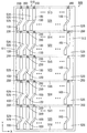
図1および図2は、本発明の一実施の形態に係る集合体シートの上面図である。また、図3は、図1の集合体シート500の一部拡大上面図である。集合体シート500は、金属製の長尺状の支持基板から作製される。なお、図1および図3においては、矢印X,Yで示すように、互いに直交する二方向をX方向およびY方向と定義する。本例では、X方向およびY方向は水平面に平行な方向である。製造時には、長尺状の支持基板に複数の集合体シート500が長手方向に並ぶように作製される。図1には、支持基板上の1つの集合体シート500が示される。
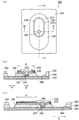
(1) Aggregate Sheet FIGS. 1 and 2 are top views of an aggregate sheet according to an embodiment of the present invention. FIG. 3 is a partially enlarged top view of the
図1に示すように、集合体シート500は、矩形状の外形を有し、支持枠510、複数の長尺状のサスペンション基板100および複数の検査用基板200を含む。図2に示すように、集合体シート500には、支持枠510より内側に領域(以下、製品保証領域と呼ぶ)550が設定される。図2においては、製品保証領域550がハッチングパターンにより示されている。製品保証領域550は、各サスペンション基板100が予め定められた仕様を満足することが保護されるべき領域である。支持枠510は、一対の側部枠511,512および複数の端部枠513,514,515,516,517,518からなる。
As shown in FIG. 1, the
一対の側部枠511,512は、互いに対向するとともにY方向に延びている。端部枠513〜518は、それぞれ一対の側部枠511,512に直交するX方向に延び、一対の側部枠511,512間をつなぐように形成されている。端部枠513〜518は、一対の側部枠511,512の一端部から他端部にかけて等間隔でY方向に並んでいる。これにより、製品保証領域550の内側には、側部枠511,512および端部枠513〜518により仕切られた複数(本例では5つ)の矩形領域521,522,523,524,525が形成されている。図2においては、製品保証領域550の内側の矩形領域521〜525が太い実線により囲まれている。
The pair of side frames 511 and 512 face each other and extend in the Y direction. The end frames 513 to 518 extend in the X direction orthogonal to the pair of side frames 511 and 512, respectively, and are formed to connect the pair of side frames 511 and 512. The end frames 513 to 518 are arranged in the Y direction at equal intervals from one end of the pair of side frames 511 and 512 to the other end. As a result, a plurality (five in this example) of
複数のサスペンション基板100は、矩形領域521〜525内でY方向に延びかつX方向に並ぶように設けられている。各サスペンション基板100の外周縁部に沿って分離溝526が形成されている。
The plurality of
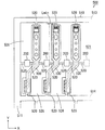
図3に示すように、各サスペンション基板100のY方向における両端は、連結部520を介して支持枠510に連結されている。本実施の形態においては、複数の検査用基板200は、複数のサスペンション基板100にそれぞれ対応するように、複数のサスペンション基板100の一端側の端部枠513〜517内に形成される。図3の例においては、矩形領域521内の複数のサスペンション基板100にそれぞれ対応する複数の検査用基板200が端部枠513内に形成される。
As shown in FIG. 3, both ends of each
同様に、矩形領域522内の複数のサスペンション基板100にそれぞれ対応する複数の検査用基板200が端部枠内514に形成される。矩形領域523内の複数のサスペンション基板100にそれぞれ対応する複数の検査用基板200が端部枠515内に形成される。矩形領域524内の複数のサスペンション基板100にそれぞれ対応する複数の検査用基板200が端部枠516内に形成される。矩形領域525内の複数のサスペンション基板100にそれぞれ対応する複数の検査用基板200が端部枠517内に形成される。本実施の形態においては、複数のサスペンション基板100と複数の検査用基板200とが一対一に対応している。
Similarly, a plurality of
複数の検査用基板200とこれらにそれぞれ対応する複数のサスペンション基板100との間の距離は互いに等しい。図3の例において、各サスペンション基板100とこれに対応する検査用基板200との間の最短距離をLminで示す。最短距離Lminは、0μm以上12000μm以下であることが好ましく、500μm以上6000μm以下であることがより好ましい。後述する図12〜図16においても同様である。この場合、後述するサスペンション基板100のビア128,129の状態と検査用基板200のビア221の状態との相関性をより高くすることができる。
The distances between the plurality of
このようにして、各矩形領域521〜525において、複数のサスペンション基板100が整列状態で支持枠510に支持される。また、複数の検査用基板200が端部枠513〜517に形成される。したがって、支持枠510を大型化することなくより多数のサスペンション基板100および検査用基板200を集合体シート500に形成することができる。これにより、集合体シート500の製造コストを低減することができる。集合体シート500の製造後、連結部520が切断されることにより、各サスペンション基板100が支持枠510から分離される。
In this way, in each of the
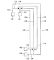
(2)サスペンション基板の構造
図4は、図1のサスペンション基板100の上面図である。図4に示すように、サスペンション基板100は、金属製の長尺状基板により形成される支持基板110を備える。支持基板110上には、太い点線で示すように、書込用配線パターン120,130および読取用配線パターン140,150が形成されている。図4では、書込用配線パターン120,130が一本の点線で示され、読取用配線パターン140,150が一本の点線で示される。書込用配線パターン120と書込用配線パターン130とは、一対の信号線路対を構成する。また、読取用配線パターン140と読取用配線パターン150とは、一対の信号線路対を構成する。
(2) Structure of Suspension Board FIG. 4 is a top view of the
支持基板110の先端部には、U字状の開口部111を形成することにより磁気ヘッド搭載部(以下、タング部と呼ぶ)112が設けられている。タング部112は、支持基板110に対して所定の角度をなすように破線Rの箇所で折り曲げ加工される。タング部112の端部には4つの電極パッド161,162,163,164が形成されている。
A magnetic head mounting portion (hereinafter referred to as a tongue portion) 112 is provided at the distal end portion of the
支持基板110の他端部には4つの電極パッド165,166,167,168が形成されている。タング部112上の電極パッド161〜164と支持基板110の他端部の電極パッド165〜168とは、それぞれ書込用配線パターン120,130および読取用配線パターン140,150により電気的に接続されている。また、支持基板110には複数の孔部113が形成されている。
Four
サスペンション基板100を備える図示しないハードディスクドライブ装置においては、磁気ディスクに対する情報の書込み時に一対の書込用配線パターン120,130に電流が流れる。また、磁気ディスクに対する情報の読取り時に一対の読取用配線パターン140,150に電流が流れる。
In a hard disk drive device (not shown) including the
(3)書込用配線パターン
次に、書込用配線パターン120,130の詳細な構成について説明する。図5は、書込用配線パターン120,130の構成を示す模式図である。図5に示すように、書込用配線パターン120は、線路121〜125により構成される。電極パッド161に線路121が接続され、電極パッド165に線路122が接続される。
(3) Write Wiring Pattern Next, the detailed configuration of the
線路123,124の一端部は、線路121に一体化する。線路123の他端部と線路125の一端部とが交差領域114において電気的に接続される。交差領域114の詳細については後述する。線路124,125の他端部は、線路122に一体化する。
One ends of the
書込用配線パターン130は、線路131〜135により構成される。電極パッド162に線路131が接続され、電極パッド166に線路132が接続される。線路133,134の一端部は、線路131に一体化する。線路133の他端部と線路135の一端部とが交差領域115において電気的に接続される。交差領域115の詳細については後述する。線路134,135の他端部は、線路132に一体化する。
The
書込用配線パターン120の線路123,124と書込用配線パターン130の線路134,135とは、互いに交互にかつ平行に配置される。書込用配線パターン120の線路123は、交差領域115において書込用配線パターン130の線路133,135の端部間を通って延び、書込用配線パターン130の線路135は、交差領域114において書込用配線パターン120の線路123,125の端部間を通って延びる。
The
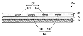
図6は、書込用配線パターン120,130の線路123,124,134,135およびその周辺部分の模式的断面図である。図6に示すように、支持基板110上にベース絶縁層170が形成される。ベース絶縁層170上に書込用配線パターン120,130の線路123,124,134,135が形成される。書込用配線パターン120,130を覆うように、ベース絶縁層170上にカバー絶縁層180が形成される。
FIG. 6 is a schematic cross-sectional view of the
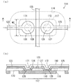
図7は、図5の交差領域114およびその周辺を示す図である。図7(a)は交差領域114の詳細な平面図を示し、図7(b)は図7(a)のA−A線断面図を示す。なお、交差領域115は、交差領域114と同様の構成を有する。
FIG. 7 is a diagram showing the
図7(a)および図7(b)に示すように、支持基板110に、環状の開口116が形成される。これにより、支持基板110の他の領域から電気的に分離された島状の領域117が形成される。支持基板110の領域117上を通って延びるように書込用配線パターン130の線路135が配置され、線路135の両側に書込用配線パターン120の線路123の端部および線路125の端部が配置される。
As shown in FIGS. 7A and 7B, an
線路123の端部および線路125の端部には、円形の接続部126,127がそれぞれ設けられる。また、接続部126,127の下方におけるベース絶縁層170の部分に、貫通孔171,172がそれぞれ形成される。貫通孔171,172は、ベース絶縁層170の上面から下面にかけて径が漸次小さくなるようにテーパ形状に形成される。
接続部126は、貫通孔171内において支持基板110の領域117に接触し、接続部127は、貫通孔172内において支持基板110の領域117に接触する。貫通孔171内の接続部126の部分によりビア128が形成され、貫通孔172内の接続部127の部分によりビア129が形成される。これにより、ビア128,129および支持基板110の領域117を介して、線路123,125が電気的に接続される。
The
接続部126の直径は線路123の幅より大きいことが好ましく、接続部127の直径は線路125の幅より大きいことが好ましい。また、ベース絶縁層170の貫通孔171の直径は線路123の幅より大きいことが好ましく、貫通孔172の直径は線路125の幅より大きいことが好ましい。それにより、線路123,125間の電気的接続性が十分に確保される。
The diameter of the
なお、支持基板110の領域117の幅WCは、接続部126との接触部分および接続部127との接触部分の間において、一定であることが好ましい。その場合、支持基板110の領域117における伝送損失が低減される。
Note that the width WC of the
また、接続部126,127の形状は、円形に限らず、楕円形、三角形、四角形または扇形等の他の形状であってもよい。また、貫通孔171,172の横断面形状は、楕円形、三角形、四角形または扇形等の他の形状であってもよい。
Moreover, the shape of the
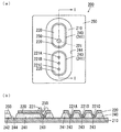
(4)検査用基板の構造
図8は、検査用基板200の構成を示す図である。図8(a)は、検査用基板200の上面図を示す。図8(b)は、図8(a)のB−B線断面図を示す。図8(c)は、図8(a)のC−C線断面図を示す。
(4) Structure of Inspection Substrate FIG. 8 is a diagram showing the configuration of the
図8に示すように、検査用基板200は、金属製の長尺状基板により形成される支持基板210を備える。支持基板210上にベース絶縁層240が形成される。ベース絶縁層240に環状の開口244が形成される。これにより、ベース絶縁層240が島状の内部領域241とその内部領域241を取り囲む外部領域242とに分離される。内部領域241と外部領域242との間の開口244から支持基板210が露出する。
As shown in FIG. 8, the
ベース絶縁層240の内部領域241に貫通孔243が形成される。貫通孔243は、ベース絶縁層240の上面から下面にかけて径が漸次小さくなるようにテーパ形状に形成される。貫通孔243の横断面形状は、円形、楕円形、三角形、四角形または扇形等の他の形状であってもよい。
A through
内部領域241上に導体層220が形成される。導体層220の一部が貫通孔243内において支持基板210に接触する。貫通孔243内の導体層220の部分によりビア221が形成される。これにより、ビア221を介して導体層220と支持基板210とが電気的に接続される。図7の支持基板110のビア128,129と支持基板210のビア221とは同じ構成を有する。
A
本例においては、検査用基板200は、図2の集合体シート500の製品保証領域550の内側に形成される。少なくとも、検査用基板200のビア221は、集合体シート500の製品保証領域550の内側に形成される。
In this example, the
導体層220のビア221の部分を除いて、導体層220の表面にめっき層230が形成される。ベース絶縁層240の外部領域242および導体層220のビア221を覆うようにカバー絶縁層250が形成される。
A
開口244は、支持基板210の図8(c)のG部の100μm以上1500μm以下の長さの部分が露出するように形成されることが好ましい。この場合、ビア221の電気的特性を検査する際に、開口244内で露出した支持基板210に検査装置のプローブをより容易に接触させることができる。これにより、ビア221の電気的特性をより効率よくかつ容易に検査することができる。
また、カバー絶縁層250は、導体層220の図8(c)のH部の100μm以上1500μm以下の長さの部分がカバー絶縁層250から露出するように形成されることが好ましい。この場合、ビア221の電気的特性を検査する際に、露出した導体層220に検査装置のプローブをより容易に接触させることができる。これにより、ビア221の電気的特性をより効率よくかつ容易に検査することができる。
The
本例においては、貫通孔243(図8(b)のD部)の最小の径は、10μm以上100μm以下に設定される。導体層220の最も短い部分(図8(b)のE部)の長さは、100μm以上1500μm以下に設定される。開口244の最も短い部分(図8(b)のF部)の幅は、30μm以上500μm以下に設定される。開口244の最も長い部分(図8(c)のG部)の幅は、100μm以上1500μm以下に設定される。カバー絶縁層250から露出する導体層220の最も長い部分(図8(c)のH部)の長さは、100μm以上1500μm以下に設定される。
In this example, the minimum diameter of the through hole 243 (D portion in FIG. 8B) is set to 10 μm or more and 100 μm or less. The length of the shortest part (E part of FIG.8 (b)) of the
(5)集合体シートの製造方法
次に、集合体シート500の製造方法について説明する。本例においては、長尺状の支持基板上にロール・トゥ・ロール方式により複数の集合体シート500が形成される。図9、図10および図11は、本発明の一実施の形態に係る集合体シート500の製造方法の一例を示す工程断面図である。図9(a)〜図11(b)の上段の図は、図7のA−A線断面に対応する。図9(a)〜図11(b)の下段の図は、図8のB−B線断面に対応する。
(5) Manufacturing method of assembly sheet Next, the manufacturing method of the
まず、図9(a)に示すように、ステンレス鋼からなる長尺状の支持基板530上にポリイミドからなるベース絶縁層540を形成する。支持基板530とベース絶縁層540との積層構造を有する2層基材を用いてもよい。
First, as shown in FIG. 9A, a
支持基板530の材料は、ステンレス鋼に限らず、アルミニウム(Al)等の他の金属材料を用いてもよい。支持基板530の厚みは、例えば10μm以上30μm以下であり、12μm以上20μm以下であることが好ましい。ベース絶縁層540の材料は、ポリイミドに限らず、エポキシ等の他の樹脂材料を用いてもよい。ベース絶縁層540の厚みは、例えば3μm以上20μm以下であり、5μm以上15μm以下であることが好ましい。
The material of the
次に、図9(b)に示すように、ベース絶縁層540を例えばエッチングすることにより、サスペンション基板100用のベース絶縁層170を形成するとともに、検査用基板200用のベース絶縁層240を形成する。同時に、図5の交差領域114,115において、ベース絶縁層170の部分に貫通孔171,172を形成する。また、ベース絶縁層240に環状の開口244を形成することにより内部領域241および外部領域242を形成し、内部領域241に貫通孔243を形成する。貫通孔171,172の最小の直径は例えば10μm以上200μm以下であり、20μm以上100μm以下であることが好ましい。
Next, as shown in FIG. 9B, the
続いて、図10(a)に示すように、電解めっき等によりベース絶縁層170上に銅からなる図4の書込用配線パターン120,130、読取用配線パターン140,150および電極パッド161〜168を形成するとともに、ベース絶縁層240上に銅からなる導体層220を形成する。図10(a)においては、書込用配線パターン120のうち線路123,125および接続部126,127の部分ならびに書込用配線パターン130のうち線路135の部分のみが図示されている。
Subsequently, as shown in FIG. 10A, the
貫通孔171内の接続部126の部分がビア128となり、貫通孔172内の接続部127の部分がビア129となり、貫通孔243内の導体層220の部分がビア221となる。書込用配線パターン120,130および読取用配線パターン140,150ならびに導体層220は、アディティブ法を用いて形成してもよく、セミアディティブ法を用いて形成してもよく、またはサブトラクティブ法等の他の方法を用いて形成してもよい。
The
書込用配線パターン120,130、読取用配線パターン140,150、電極パッド161〜168および導体層220の材料は、銅に限らず、金(Au)もしくはアルミニウム等の他の金属、または銅合金もしくはアルミニウム合金等の合金を用いてもよい。書込用配線パターン120,130および読取用配線パターン140,150の厚みは、例えば3μm以上16μm以下であり、4μm以上13μm以下であることが好ましい。書込用配線パターン120,130および読取用配線パターン140,150の幅は、例えば6μm以上200μm以下であり、8μm以上150μm以下であることが好ましい。
The materials of the
その後、図10(b)に示すように、書込用配線パターン120,130および読取用配線パターン140,150を覆うように、ベース絶縁層170上にポリイミドからなるカバー絶縁層180を形成する。同時に、ベース絶縁層240の外部領域242および導体層220のビア221を覆うようにポリイミドからなるカバー絶縁層250を形成する。カバー絶縁層180,250の材料は、ポリイミドに限定されず、エポキシ等の他の絶縁材料を用いてもよい。カバー絶縁層180,250の厚みは、例えば1μm以上30μm以下であり、3μm以上10μm以下であることが好ましい。
Thereafter, as shown in FIG. 10B, a
次に、図11(a)に示すように、導体層220のビア221の部分を除いて、導体層220の表面に例えば金(Au)からなるめっき層230を形成する。同時に、図4の電極パッド161〜168の表面にめっき層230と同様のめっき層を形成する。
Next, as shown in FIG. 11A, a
続いて、支持基板530を例えばエッチングすることにより、支持基板530に図1の分離溝526を形成するとともに、図5の交差領域114,115において、図7(b)の環状の開口116を形成する。同時に、支持基板530に図4の開口部111および複数の孔部113を形成する。また、長尺状の支持基板530を一定間隔で切断することにより個々の集合体シート500を分離する。
Subsequently, the
これにより、図11(b)に示すように、サスペンション基板100用の支持基板110、検査用基板200用の支持基板210、図3の支持枠510および連結部520が形成される。また、支持基板110に環状の開口116が形成されるとともに、支持基板110に他の領域から分離された領域117が形成される。領域117の面積は、例えば1800μm2以上180000μm2以下であり、3200μm2以上80000μm2以下であることが好ましい。
Thus, as shown in FIG. 11B, the
以上の工程により、複数のサスペンション基板100、複数の検査用基板200および支持枠510を含む集合体シート500が完成する。
Through the above steps, the
(6)検査用基板の検査
集合体シート500に形成された検査用基板200のビア221の検査を行う。例えば、検査装置の一のプローブを検査用基板200のめっき層230に接触させ、他のプローブを検査用基板200の開口244内で露出した支持基板210に接触させる。それにより、ビア221の抵抗値を測定することができる。
(6) Inspection of the inspection substrate The inspection of the via 221 of the
この場合、後述するように、複数の検査用基板200のビア221の抵抗値とこれらに対応する複数のサスペンション基板100のビア128,129の抵抗値とは高い相関性を有する。そのため、複数の検査用基板200のビア221の抵抗値を測定することによりこれらに対応する複数のサスペンション基板100のビア128,129の電気的特性の良否を検査することができる。したがって、複数のサスペンション基板100のビア128,129の検査を短時間で行うことができるとともに、検査結果の信頼性を向上させることができる。
In this case, as will be described later, the resistance values of the
検査後、集合体シート500の複数の連結部520を切断することにより、支持枠510から複数のサスペンション基板100を分離することができる。
After the inspection, the plurality of
(7)変形例
(a)第1の変形例
上記実施の形態においては、複数の検査用基板200は、複数のサスペンション基板100の一端側の端部枠513〜517内に形成されるが、これに限定されない。複数の検査用基板200は、支持枠510のいずれの部分に形成されてもよい。
(7) Modification (a) First Modification In the above embodiment, the plurality of
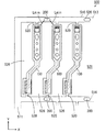
図12は、第1の変形例に係る集合体シート500の上面図である。図12の例においては、複数の検査用基板200は、複数のサスペンション基板100にそれぞれ対応するように、複数のサスペンション基板100の他端側の端部枠514〜518に形成される。具体的には、矩形領域521〜525内の複数のサスペンション基板100にそれぞれ対応する複数の検査用基板200が端部枠514〜518内に形成される。本例においても、複数のサスペンション基板100と複数の検査用基板200とが一対一に対応している。
FIG. 12 is a top view of the
(b)第2の変形例
上記実施の形態においては、複数の検査用基板200は、支持枠510に形成されるが、これに限定されない。複数の検査用基板200は、集合体シート500の製品保証領域550のいずれの部分に形成されてもよい。
(B) Second Modification In the above embodiment, the plurality of
図13は、第2の変形例に係る集合体シート500の一部拡大上面図である。図13の例においては、矩形領域521内の複数のサスペンション基板100にそれぞれ対応する複数の検査用基板200が矩形領域521内に形成される。複数の検査用基板200は、それぞれ複数の連結部520を介して端部枠513に接続される。
FIG. 13 is a partially enlarged top view of the
同様に、矩形領域522内の複数のサスペンション基板100にそれぞれ対応する複数の検査用基板200が矩形領域522内に形成される。複数の検査用基板200は、それぞれ複数の連結部520を介して端部枠514に接続される。矩形領域523内の複数のサスペンション基板100にそれぞれ対応する複数の検査用基板200が矩形領域523内に形成される。複数の検査用基板200は、それぞれ複数の連結部520を介して端部枠515に接続される。
Similarly, a plurality of
矩形領域524内の複数のサスペンション基板100にそれぞれ対応する複数の検査用基板200が矩形領域524内に形成される。複数の検査用基板200は、それぞれ複数の連結部520を介して端部枠516に接続される。矩形領域525内の複数のサスペンション基板100にそれぞれ対応する複数の検査用基板200が矩形領域525内に形成される。複数の検査用基板200は、それぞれ複数の連結部520を介して端部枠517に接続される。
A plurality of
本例においても、複数のサスペンション基板100と複数の検査用基板200とが一対一に対応している。本例においては、複数の検査用基板200は、複数のサスペンション基板100に近い位置に配置されるので、ビア128,129の状態とビア221の状態との相関性をより高くすることができる。
Also in this example, the plurality of
(c)第3の変形例
図14は、第3の変形例に係る集合体シート500の一部拡大上面図である。図14の例においては、複数のサスペンション基板100にそれぞれ対応する複数の検査用基板200がX方向に隣り合うように配置される。具体的には、各2つのサスペンション基板100間の分離溝526内に各検査用基板200が配置され、各検査用基板200は連結部520により両隣のサスペンション基板100に支持される。また、X方向における一端部のサスペンション基板100と側部枠511との間の分離溝526内に1つの検査用基板200が設けられる。
(C) Third Modification FIG. 14 is a partially enlarged top view of an
本例においても、複数のサスペンション基板100と複数の検査用基板200とが一対一に対応している。また、第2の変形例と同様に、複数の検査用基板200は、複数のサスペンション基板100に近い位置に配置されるので、ビア128,129の状態とビア221の状態との相関性をより高くすることができる。
Also in this example, the plurality of
(d)第4の変形例
上記実施の形態においては、各サスペンション基板100に対応して1個の検査用基板200が設けられるが、これに限定されない。各サスペンション基板100に対応して2個以上の検査用基板200が設けられてもよい。
(D) Fourth Modification In the above embodiment, one
図15は、第4の変形例に係る集合体シート500の一部拡大上面図である。図15の例においては、各1個のサスペンション基板100と2個の検査用基板200が対応している。具体的には、矩形領域521内の各サスペンション基板100の一端部に対応する検査用基板200が端部枠513内に形成され、他端部に対応する検査用基板200が端部枠514内に形成される。
FIG. 15 is a partially enlarged top view of an
同様に、矩形領域522内の各サスペンション基板100の一端部に対応する検査用基板200が端部枠514内に形成され、他端部に対応する検査用基板200が端部枠515内に形成される。矩形領域523内の各サスペンション基板100の一端部に対応する検査用基板200が端部枠515内に形成され、他端部に対応する検査用基板200が端部枠516内に形成される。
Similarly, an
矩形領域524内の各サスペンション基板100の一端部に対応する検査用基板200が端部枠516内に形成され、他端部に対応する検査用基板200が端部枠517内に形成される。矩形領域525内の各サスペンション基板100の一端部に対応する検査用基板200が端部枠517内に形成され、他端部に対応する検査用基板200が端部枠518内に形成される。
An
(e)第5の変形例
2個以上のサスペンション基板100に対応して1個の検査用基板200が設けられてもよい。図16は、第5の変形例に係る集合体シート500の一部拡大上面図である。図16の例においては、各2個のサスペンション基板100と1個の検査用基板200が対応している。具体的には、矩形領域521内の各2個のサスペンション基板100の一端部に対応する検査用基板200が端部枠513内に形成される。
(E) Fifth Modification One
同様に、矩形領域522内の各2個のサスペンション基板100の一端部に対応する検査用基板200が端部枠514内に形成される。矩形領域523内の各2個のサスペンション基板100の一端部に対応する検査用基板200が端部枠515に形成される。矩形領域524内の各2個のサスペンション基板100の一端部に対応する検査用基板200が端部枠516内に形成される。矩形領域525内の各2個のサスペンション基板100の一端部に対応する検査用基板200が端部枠517内に形成される。
Similarly, an
(f)第6の変形例
上記実施の形態において、一の検査用基板200に一のビア221が設けられるが、これに限定されない。一の検査用基板200に複数種類のビア221が設けられてもよい。図17は、第6の変形例に係る集合体シート500の検査用基板200の構成を示す図である。図17(a)は、検査用基板200の上面図を示す。図17(b)は、図17(a)のI−I線断面図を示す。
(F) Sixth Modification Although one via 221 is provided in one
図17に示すように、第6の変形例における検査用基板200においては、ベース絶縁層240の環状の開口244内に島状の一の内部領域241および島状の他の内部領域241が形成される。一の内部領域241には、一のビア221が形成される。一方、他の内部領域241には複数(本例では3つ)のビア221A,221B,221Cが形成される。
As shown in FIG. 17, in the
本例においては、他の内部領域241の複数のビア221A〜221Cの径は、一の内部領域241のビア221の径よりも小さい。ビア221,221A〜221Cは、サスペンション基板100に形成される複数種類のビア(図示せず)にそれぞれ対応する構成および寸法を有する。これにより、一の検査用基板200を用いて各サスペンション基板100の複数種類のビアを検査することができる。
In this example, the diameters of the plurality of
なお、図17に示すように、導体層220には図8のめっき層230が形成されなくてもよい。また、ビア221,221A〜221Cの一部または全部には、カバー絶縁層250が形成されなくてもよい。図17の例においては、ビア221A〜221Cにはカバー絶縁層250が形成されない。
As shown in FIG. 17, the
(8)効果
本実施の形態に係る集合体シート500においては、複数のサスペンション基板100が支持枠510により一体的に支持される。また、複数の検査用基板200が複数のサスペンション基板100に対応するように支持枠510に設けられる。ここで、複数のサスペンション基板100のビア128,129と検査用基板200のビア221とは同じ構成を有する。
(8) Effect In the
それにより、ビア128,129の状態とビア221の状態とが高い相関性を有する。したがって、検査用基板200のビア221の検査を行うことにより、複数のサスペンション基板100のビア128,129の検査を短時間で行うことができるとともに、検査結果の信頼性を向上させることができる。
Thereby, the state of the
本実施の形態においては、複数の検査用基板200が支持枠510内に設けられるので、複数の検査用基板200を配置するスペースを別個に設ける必要がない。また、複数の検査用基板200を支持枠510に支持するための連結部を設ける必要がない。これにより、サスペンション基板100の構成を単純化し、かつサスペンション基板100を小型化することができる。さらに、治具式の検査装置により複数のサスペンション基板100の抵抗値の検査と同時に複数の検査用基板200の検査を容易に行うことができる。
In the present embodiment, since the plurality of
また、本実施の形態においては、複数のサスペンション基板100と複数の検査用基板200とが一対一に対応するので、サスペンション基板100ごとのビア128,129の状態を検査することができる。これにより、サスペンション基板100ごとの検査結果の信頼性を向上させることができる。さらに、多数のサスペンション基板100が検査されるので、検査結果の信頼性をより向上させることができる。
In the present embodiment, since the plurality of
複数の検査用基板200とこれらにそれぞれ対応する複数のサスペンション基板100との間の距離は互いに等しい。この場合、複数のサスペンション基板100および複数の検査用基板200において、ビア128,129の状態とビア221の状態との相関性が互いに等しくなる。そのため、複数の検査用基板200の検査結果を比較することにより、検査結果の信頼性をさらに向上させることができる。
The distances between the plurality of
また、本実施の形態に係る集合体シート500においては、カバー絶縁層180によりビア128,129が腐食することが防止されるとともに、カバー絶縁層250によりビア221が腐食することが防止される。これにより、検査用基板200のビア221の状態と複数のサスペンション基板100のビア128,129の状態との経時的な相関性の低下を防止することができる。
Further, in
(9)実施例
実施例1〜8として、図1に示す構成を有する集合体シート500を作製した。集合体シート500に含まれる8個の検査用基板200を選択し、選択された検査用基板200のビア221の抵抗値およびそれらに対応するサスペンション基板100のビア128の抵抗値を測定した。
(9) Examples As Examples 1 to 8, an
ここで、検査用基板200のビア221の抵抗値は図8の支持基板210とめっき層230との間の抵抗値であり、サスペンション基板100のビア128の抵抗値は図7の支持基板110と接続部126との間の抵抗値である。検査用基板200のビア221の抵抗値およびサスペンション基板100のビア128の抵抗値の測定結果を表1に示す。
Here, the resistance value of the via 221 of the

表1に示すように、実施例1の検査用基板200のビア221の抵抗値は0.133Ωであり、これに対応するサスペンション基板100のビア128の抵抗値は0.156Ωであった。実施例2の検査用基板200のビア221の抵抗値は0.169Ωであり、これに対応するサスペンション基板100のビア128の抵抗値は0.174Ωであった。
As shown in Table 1, the resistance value of the via 221 of the
実施例3の検査用基板200のビア221の抵抗値は0.185Ωであり、これに対応するサスペンション基板100のビア128の抵抗値は0.208Ωであった。実施例4の検査用基板200のビア221の抵抗値は0.170Ωであり、これに対応するサスペンション基板100のビア128の抵抗値は0.193Ωであった。
The resistance value of the via 221 of the
実施例5の検査用基板200のビア221の抵抗値は0.181Ωであり、これに対応するサスペンション基板100のビア128の抵抗値は0.175Ωであった。実施例6の検査用基板200のビア221の抵抗値は0.205Ωであり、これに対応するサスペンション基板100のビア128の抵抗値は0.224Ωであった。
The resistance value of the via 221 of the
実施例7の検査用基板200のビア221の抵抗値は0.172Ωであり、これに対応するサスペンション基板100のビア128の抵抗値は0.169Ωであった。実施例8の検査用基板200のビア221の抵抗値は0.288Ωであり、これに対応するサスペンション基板100のビア128の抵抗値は0.295Ωであった。
The resistance value of the via 221 of the
図18は、検査用基板200のビア221の抵抗値とサスペンション基板100のビア128の抵抗値との関係を示す図である。図18の横軸は検査用基板200のビア221の抵抗値を示し、縦軸はサスペンション基板100のビア128の抵抗値を示す。
FIG. 18 is a diagram illustrating the relationship between the resistance value of the via 221 of the
図18に示すように、実施例1〜8においては、検査用基板200のビア221の抵抗値は、サスペンション基板100のビア128の抵抗値の変化に略線形に依存して変化する。これにより、検査用基板200のビア221の抵抗値とサスペンション基板100のビア128の抵抗値とが高い相関性を有することが確認された。
As shown in FIG. 18, in the first to eighth embodiments, the resistance value of the via 221 of the
(10)請求項の各構成要素と実施の形態の各部との対応関係
以下、請求項の各構成要素と実施の形態の各部との対応の例について説明するが、本発明は下記の例に限定されない。
(10) Correspondence between each component of claim and each part of embodiment The following describes an example of a correspondence between each component of the claim and each part of the embodiment. It is not limited.
集合体シート500が回路付きサスペンション基板集合体シートの例であり、支持基板110,210がそれぞれ第1および第2の支持基板の例であり、ベース絶縁層170,240がそれぞれ第1および第2の絶縁層の例である。書込用配線パターン120,130が導体線路の例であり、導体層220が導体層の例であり、カバー絶縁層180,250がそれぞれ第3および第4の絶縁層の例である。ビア128,129が第1のビアの例であり、ビア221が第2のビアの例であり、開口244が開口部の例であり、支持基板530が支持基板の例であり、ベース絶縁層540が絶縁層の例である。
The
請求項の各構成要素として、請求項に記載されている構成または機能を有する他の種々の要素を用いることもできる。
(11)参考形態
(11−1)第1の参考形態に係る回路付きサスペンション基板集合体シートは、複数の回路付きサスペンション基板と、複数の回路付きサスペンション基板を一体的に支持する支持枠と、複数の回路付きサスペンション基板に対応するように設けられる複数の検査用基板とを備え、複数の回路付きサスペンション基板の各々は、導電性の第1の支持基板と、第1の支持基板上に形成された第1の絶縁層と、第1の絶縁層上に形成された導体線路と、第1の絶縁層内を通って第1の支持基板と導体線路とを電気的に接続する第1のビアとを含み、複数の検査用基板の各々は、導電性の第2の支持基板と、第2の支持基板上に形成された第2の絶縁層と、第2の絶縁層上に形成された導体層と、第2の絶縁層内を通って第2の支持基板と導体層とを電気的に接続する第2のビアとを含み、第1のビアと第2のビアとは同じ構成を有するものである。
この回路付きサスペンション基板集合体シートにおいては、複数の回路付きサスペンション基板が支持枠により一体的に支持される。複数の検査用基板が複数の回路付きサスペンション基板に対応するように設けられる。複数の回路付きサスペンション基板の各々においては、導電性の第1の支持基板上に第1の絶縁層が形成される。第1の絶縁層上に導体線路が形成される。第1の支持基板と導体線路とが第1の絶縁層内を通る第1のビアにより電気的に接続される。複数の検査用基板の各々においては、導電性の第2の支持基板上に第2の絶縁層が形成される。第2の絶縁層上に導体層が形成される。第2の支持基板と導体層とが第2の絶縁層内を通る第2のビアにより電気的に接続される。
この場合、複数の検査用基板は、複数の回路付きサスペンション基板に対応するように形成され、かつ、複数の回路付きサスペンション基板の第1のビアと検査用基板の第2のビアとは同じ構成を有する。それにより、第1のビアの状態と第2のビアの状態とが高い相関性を有する。したがって、検査用基板の第2のビアの検査を行うことにより、複数のサスペンション基板の第1のビアの検査を短時間で行うことができるとともに、検査結果の信頼性を向上させることができる。
(11−2)複数の検査用基板は、支持枠内に配置されてもよい。この場合、複数の検査用基板を配置するスペースを別個に設ける必要がない。また、複数の検査用基板を支持枠に支持するための他の部材を設ける必要がない。これにより、回路付きサスペンション基板集合体シートの構成を単純化し、かつ回路付きサスペンション基板集合体シートを小型化することができる。
(11−3)支持枠は、複数の回路付きサスペンション基板の少なくとも一部を取り囲み、複数の検査用基板は、支持枠により取り囲まれる領域に配置されてもよい。
この場合、複数の検査用基板は、複数の回路付きサスペンション基板に近い位置に配置される。これにより、第1のビアの状態と第2のビアの状態との相関性を高くすることができる。
(11−4)複数の検査用基板と複数の検査用基板に対応する複数の回路付きサスペンション基板との間の距離は互いに等しくてもよい。
この場合、複数の回路付きサスペンション基板および複数の検査用基板において、第1のビアの状態と第2のビアの状態との相関性が互いに等しくなる。そのため、複数の検査用基板の検査結果を比較することにより、検査結果の信頼性をさらに向上させることができる。
(11−5)複数の検査用基板の各々と対応する回路付きサスペンション基板との間の最短距離は0μm以上12000μm以下であってもよい。
この場合、第1のビアの状態と第2のビアの状態との相関性をより高くすることができる。
(11−6)複数の回路付きサスペンション基板の各々について1または複数の検査用基板が対応するように、複数の回路付きサスペンション基板および複数の検査用基板が設けられてもよい。
この場合、回路付きサスペンション基板ごとの第1のビアの状態を検査することができる。これにより、回路付きサスペンション基板ごとの検査結果の信頼性を向上させることができる。
(11−7)第2の絶縁層は、第2の支持基板の一部が露出するように形成される開口部を有してもよい。
この場合、第2のビアの電気的特性を検査する際に、開口部内で露出した第2の支持基板に検査装置のプローブを容易に接触させることができる。これにより、第2のビアの電気的特性を効率よくかつ容易に検査することができる。
(11−8)開口部は、第2の支持基板の100μm以上の長さの部分が露出するように形成されてもよい。
この場合、第2のビアの電気的特性を検査する際に、開口部内で露出した第2の支持基板に検査装置のプローブをより容易に接触させることができる。これにより、第2のビアの電気的特性をより効率よくかつ容易に検査することができる。
(11−9)複数の回路付きサスペンション基板は、導体線路の少なくとも一部および第1のビアを覆うように第1の絶縁層上に形成される第3の絶縁層をさらに含み、検査用基板は、第2のビアを覆うとともに導体層の少なくとも一部が露出するように第2の絶縁層上に形成される第4の絶縁層をさらに含んでもよい。
この場合、第2のビアの電気的特性を検査する際に、露出した導体層に検査装置のプローブを容易に接触させることができる。これにより、第2のビアの電気的特性を効率よくかつ容易に検査することができる。また、第3の絶縁層により第1のビアが腐食することが防止されるとともに、第4の絶縁層により第2のビアが腐食することが防止される。これにより、検査用基板の第2のビアの状態と複数の回路付きサスペンション基板の第1のビアの状態との経時的な相関性の低下を防止することができる。
(11−10)第4の絶縁層は、導体層の100μm以上の長さの部分が露出するように形成されてもよい。
この場合、第2のビアの電気的特性を検査する際に、露出した導体層に検査装置のプローブをより容易に接触させることができる。これにより、第2のビアの電気的特性をより効率よくかつ容易に検査することができる。
(11−11)複数の回路付きサスペンション基板は、整列状態で支持枠に支持されてもよい。
この場合、支持枠を大型化することなくより多数の回路付きサスペンション基板および検査用基板を回路付きサスペンション基板集合体シートに設けることができる。これにより、回路付きサスペンション基板集合体シートの製造コストを低減することができる。
(11−12)第2の参考形態に係る回路付きサスペンション基板集合体シートの製造方法は、導電性の支持基板と絶縁層との積層構造を有する基材を用意する工程と、絶縁層を加工することにより、複数の回路付きサスペンション基板用の複数の第1の絶縁層および複数の検査用基板用の第2の絶縁層を形成する工程と、支持基板に電気的に接続される第1のビアを複数の第1の絶縁層にそれぞれ形成するとともに支持基板に電気的に接続される第2のビアを第2の絶縁層に形成し、複数の第1の絶縁層上に第1のビアに電気的に接続されるように導体線路をそれぞれ形成するとともに第2の絶縁層上に第2のビアに電気的に接続されるように導体層を形成する工程と、支持基板における複数の回路付きサスペンション基板用の領域、複数の検査用基板用の領域および支持枠用の領域を除く支持基板の領域を除去することにより、複数の回路付きサスペンション基板、複数の検査用基板および支持枠を作製する工程とを含み、複数の検査用基板は、複数の回路付きサスペンション基板に対応して設けられるものである。
この回路付きサスペンション基板集合体シートの製造方法によれば、複数の回路付きサスペンション基板が支持枠により一体的に支持される。複数の検査用基板が複数の回路付きサスペンション基板に対応するように設けられる。複数の回路付きサスペンション基板の各々においては、導電性の第1の支持基板上に第1の絶縁層が形成される。第1の絶縁層上に導体線路が形成される。第1の支持基板と導体線路とが第1の絶縁層内を通る第1のビアにより電気的に接続される。複数の検査用基板の各々においては、導電性の第2の支持基板上に第2の絶縁層が形成される。第2の絶縁層上に導体層が形成される。第2の支持基板と導体層とが第2の絶縁層内を通る第2のビアにより電気的に接続される。
この場合、複数の検査用基板は、複数の回路付きサスペンション基板に対応するように形成され、かつ、複数の回路付きサスペンション基板の第1のビアと検査用基板の第2のビアとは同じ構成を有する。それにより、第1のビアの状態と第2のビアの状態とが高い相関性を有する。したがって、検査用基板の第2のビアの検査を行うことにより、複数のサスペンション基板の第1のビアの検査を短時間で行うことができるとともに、検査結果の信頼性を向上させることができる。
As each constituent element in the claims, various other elements having configurations or functions described in the claims can be used.
(11) Reference form
(11-1) The suspension board assembly sheet with circuit according to the first reference embodiment includes a plurality of suspension boards with circuits, a support frame that integrally supports the plurality of suspension boards with circuits, and a plurality of suspensions with circuits. A plurality of inspection substrates provided to correspond to the substrate, each of the plurality of suspension boards with circuits being a conductive first support substrate and a first support substrate formed on the first support substrate. An insulating layer; a conductor line formed on the first insulating layer; and a first via that electrically connects the first support substrate and the conductor line through the first insulating layer; Each of the plurality of test substrates includes a conductive second support substrate, a second insulating layer formed on the second support substrate, a conductor layer formed on the second insulating layer, A second support substrate and a conductor layer through the second insulating layer And a second via electrically connecting the, the first via and the second via is one which has the same configuration.
In this suspension board assembly sheet with circuit, a plurality of suspension boards with circuit are integrally supported by a support frame. A plurality of test substrates are provided so as to correspond to a plurality of suspension boards with circuits. In each of the plurality of suspension boards with circuits, a first insulating layer is formed on a conductive first support board. A conductor line is formed on the first insulating layer. The first support substrate and the conductor line are electrically connected by a first via passing through the first insulating layer. In each of the plurality of inspection substrates, the second insulating layer is formed on the conductive second support substrate. A conductor layer is formed on the second insulating layer. The second support substrate and the conductor layer are electrically connected by a second via that passes through the second insulating layer.
In this case, the plurality of inspection boards are formed so as to correspond to the plurality of suspension boards with circuits, and the first vias of the plurality of suspension boards with circuits and the second vias of the inspection boards have the same configuration. Have Thereby, the state of the first via and the state of the second via have a high correlation. Therefore, by inspecting the second via of the inspection substrate, the first via of the plurality of suspension boards can be inspected in a short time, and the reliability of the inspection result can be improved.
(11-2) The plurality of inspection substrates may be arranged in the support frame. In this case, there is no need to separately provide a space for arranging a plurality of inspection substrates. Further, there is no need to provide another member for supporting the plurality of inspection substrates on the support frame. Thereby, the configuration of the suspension board assembly sheet with circuit can be simplified, and the suspension board assembly sheet with circuit can be reduced in size.
(11-3) The support frame may surround at least a part of the plurality of suspension boards with circuits, and the plurality of inspection boards may be arranged in a region surrounded by the support frame.
In this case, the plurality of inspection boards are arranged at positions close to the plurality of suspension boards with circuits. Thereby, the correlation between the state of the first via and the state of the second via can be increased.
(11-4) The distances between the plurality of inspection boards and the plurality of suspension boards with circuits corresponding to the plurality of inspection boards may be equal to each other.
In this case, the correlation between the state of the first via and the state of the second via is equal in the plurality of suspension boards with circuits and the plurality of inspection boards. Therefore, the reliability of the inspection result can be further improved by comparing the inspection results of the plurality of inspection substrates.
(11-5) The shortest distance between each of the plurality of test substrates and the corresponding suspension board with circuit may be 0 μm or more and 12000 μm or less.
In this case, the correlation between the state of the first via and the state of the second via can be further increased.
(11-6) A plurality of suspension boards with circuits and a plurality of inspection boards may be provided so that one or more inspection boards correspond to each of the plurality of suspension boards with circuits.
In this case, the state of the first via for each suspension board with circuit can be inspected. Thereby, the reliability of the inspection result for each suspension board with circuit can be improved.
(11-7) The second insulating layer may have an opening formed so that a part of the second support substrate is exposed.
In this case, when inspecting the electrical characteristics of the second via, the probe of the inspection apparatus can be easily brought into contact with the second support substrate exposed in the opening. Thereby, the electrical characteristics of the second via can be inspected efficiently and easily.
(11-8) The opening may be formed such that a portion having a length of 100 μm or more of the second support substrate is exposed.
In this case, when inspecting the electrical characteristics of the second via, the probe of the inspection apparatus can be more easily brought into contact with the second support substrate exposed in the opening. Thereby, the electrical characteristics of the second via can be inspected more efficiently and easily.
(11-9) The plurality of suspension boards with circuits further include a third insulating layer formed on the first insulating layer so as to cover at least a part of the conductor line and the first via, and the inspection board May further include a fourth insulating layer formed on the second insulating layer so as to cover the second via and expose at least part of the conductor layer.
In this case, when inspecting the electrical characteristics of the second via, the probe of the inspection apparatus can be easily brought into contact with the exposed conductor layer. Thereby, the electrical characteristics of the second via can be inspected efficiently and easily. Further, the third insulating layer prevents the first via from being corroded, and the fourth insulating layer prevents the second via from being corroded. Accordingly, it is possible to prevent a decrease in correlation over time between the state of the second via of the inspection substrate and the state of the first via of the plurality of suspension boards with circuits.
(11-10) The fourth insulating layer may be formed so that a portion having a length of 100 μm or more of the conductor layer is exposed.
In this case, when inspecting the electrical characteristics of the second via, the probe of the inspection apparatus can be more easily brought into contact with the exposed conductor layer. Thereby, the electrical characteristics of the second via can be inspected more efficiently and easily.
(11-11) The plurality of suspension boards with circuits may be supported by the support frame in an aligned state.
In this case, a larger number of suspension boards with circuits and inspection boards can be provided on the suspension board assembly sheet with circuits without increasing the size of the support frame. Thereby, the manufacturing cost of the suspension board assembly sheet with circuit can be reduced.
(11-12) A method of manufacturing a suspension board assembly sheet with circuit according to a second embodiment includes a step of preparing a base material having a laminated structure of a conductive support substrate and an insulating layer, and processing the insulating layer Thus, a step of forming a plurality of first insulating layers for a plurality of suspension boards with circuits and a second insulating layer for a plurality of inspection substrates, and a first electrically connected to the support substrate A via is formed in each of the plurality of first insulating layers and a second via electrically connected to the support substrate is formed in the second insulating layer, and the first via is formed on the plurality of first insulating layers. Forming a conductor line so as to be electrically connected to each other and forming a conductor layer on the second insulating layer so as to be electrically connected to the second via; and a plurality of circuits in the support substrate Multiple areas for suspension boards with multiple Removing a region of the support substrate excluding the region for the substrate for inspection and the region for the support frame to produce a plurality of suspension boards with circuits, a plurality of inspection substrates and a support frame, and a plurality of inspections The substrate for use is provided corresponding to a plurality of suspension boards with circuits.
According to the method of manufacturing the suspension board assembly sheet with circuit, the plurality of suspension boards with circuit are integrally supported by the support frame. A plurality of test substrates are provided so as to correspond to a plurality of suspension boards with circuits. In each of the plurality of suspension boards with circuits, a first insulating layer is formed on a conductive first support board. A conductor line is formed on the first insulating layer. The first support substrate and the conductor line are electrically connected by a first via passing through the first insulating layer. In each of the plurality of inspection substrates, the second insulating layer is formed on the conductive second support substrate. A conductor layer is formed on the second insulating layer. The second support substrate and the conductor layer are electrically connected by a second via that passes through the second insulating layer.
In this case, the plurality of inspection boards are formed so as to correspond to the plurality of suspension boards with circuits, and the first vias of the plurality of suspension boards with circuits and the second vias of the inspection boards have the same configuration. Have Thereby, the state of the first via and the state of the second via have a high correlation. Therefore, by inspecting the second via of the inspection substrate, the first via of the plurality of suspension boards can be inspected in a short time, and the reliability of the inspection result can be improved.
本発明は、種々の配線回路基板に有効に利用できる。 The present invention can be effectively used for various printed circuit boards.
100 サスペンション基板
110,210,530 支持基板
111 開口部
112 タング部
113 孔部
114,115 交差領域
116,244 開口
117 領域
120,130 書込用配線パターン
121〜125,131〜135 線路
126,127 接続部
128,129,221,221A〜221C ビア
140,150 読取用配線パターン
161〜168 電極パッド
170,240,540 ベース絶縁層
171,172,243 貫通孔
180,250 カバー絶縁層
200 検査用基板
220 導体層
230 めっき層
241 内部領域
242 外部領域
500 集合体シート
510 支持枠
511,512 側部枠
513〜517 端部枠
520 連結部
521〜525 矩形領域
526 分離溝
550 製品保証領域
DESCRIPTION OF
Claims (12)
前記複数の回路付きサスペンション基板を一体的に支持する支持枠と、
前記複数の回路付きサスペンション基板に対応するように設けられる複数の検査用基板とを備え、
前記複数の回路付きサスペンション基板の各々は、
導電性の第1の支持基板と、
前記第1の支持基板上に形成された第1の絶縁層と、
前記第1の絶縁層上に形成された導体線路と、
前記第1の絶縁層内を通って前記第1の支持基板と前記導体線路とを電気的に接続する第1のビアとを含み、
前記複数の検査用基板の各々は、
導電性の第2の支持基板と、
前記第2の支持基板上に形成された第2の絶縁層と、
前記第2の絶縁層上に形成された導体層と、
前記第2の絶縁層内を通って前記第2の支持基板と前記導体層とを電気的に接続する第2のビアとを含み、
前記第1のビアと前記第2のビアとは同じ構成を有し、
前記第2の絶縁層は、前記第2の支持基板の一部が露出するように形成される開口部を有する、回路付きサスペンション基板集合体シート。 Suspension boards with multiple circuits;
A support frame that integrally supports the plurality of suspension boards with circuits;
A plurality of inspection boards provided to correspond to the plurality of suspension boards with circuits,
Each of the plurality of suspension boards with circuits is
A conductive first support substrate;
A first insulating layer formed on the first support substrate;
A conductor line formed on the first insulating layer;
A first via that electrically connects the first support substrate and the conductor line through the first insulating layer;
Each of the plurality of inspection substrates is
A conductive second support substrate;
A second insulating layer formed on the second support substrate;
A conductor layer formed on the second insulating layer;
A second via that electrically connects the second support substrate and the conductor layer through the second insulating layer;
The first via and the second via have the same configuration,
The suspension board assembly sheet with circuit, wherein the second insulating layer has an opening formed so that a part of the second support substrate is exposed.
前記複数の回路付きサスペンション基板を一体的に支持する支持枠と、
前記複数の回路付きサスペンション基板に対応するように設けられる複数の検査用基板とを備え、
前記複数の回路付きサスペンション基板の各々は、
導電性の第1の支持基板と、
前記第1の支持基板上に形成された第1の絶縁層と、
前記第1の絶縁層上に形成された導体線路と、
前記第1の絶縁層内を通って前記第1の支持基板と前記導体線路とを電気的に接続する第1のビアとを含み、
前記複数の検査用基板の各々は、
導電性の第2の支持基板と、
前記第2の支持基板上に形成された第2の絶縁層と、
前記第2の絶縁層上に形成された導体層と、
前記第2の絶縁層内を通って前記第2の支持基板と前記導体層とを電気的に接続する第2のビアとを含み、
前記第1のビアと前記第2のビアとは同じ構成を有し、
前記複数の回路付きサスペンション基板は、前記導体線路の少なくとも一部および前記第1のビアを覆うように前記第1の絶縁層上に形成される第3の絶縁層をさらに含み、
前記検査用基板は、前記第2のビアを覆うとともに前記導体層の少なくとも一部が露出するように前記第2の絶縁層上に形成される第4の絶縁層をさらに含む、回路付きサスペンション基板集合体シート。 Suspension boards with multiple circuits;
A support frame that integrally supports the plurality of suspension boards with circuits;
A plurality of inspection boards provided to correspond to the plurality of suspension boards with circuits,
Each of the plurality of suspension boards with circuits is
A conductive first support substrate;
A first insulating layer formed on the first support substrate;
A conductor line formed on the first insulating layer;
A first via that electrically connects the first support substrate and the conductor line through the first insulating layer;
Each of the plurality of inspection substrates is
A conductive second support substrate;
A second insulating layer formed on the second support substrate;
A conductor layer formed on the second insulating layer;
A second via that electrically connects the second support substrate and the conductor layer through the second insulating layer;
The first via and the second via have the same configuration,
The plurality of suspension boards with circuits further include a third insulating layer formed on the first insulating layer so as to cover at least a part of the conductor line and the first via,
The circuit board for inspection further includes a fourth insulating layer that covers the second via and is formed on the second insulating layer so that at least a part of the conductor layer is exposed. Aggregate sheet.
前記絶縁層を加工することにより、複数の回路付きサスペンション基板用の複数の第1の絶縁層および複数の検査用基板用の第2の絶縁層を形成する工程と、
前記支持基板に電気的に接続される第1のビアを前記複数の第1の絶縁層にそれぞれ形成するとともに前記支持基板に電気的に接続される第2のビアを前記第2の絶縁層に形成し、前記複数の第1の絶縁層上に前記第1のビアに電気的に接続されるように導体線路をそれぞれ形成するとともに前記第2の絶縁層上に前記第2のビアに電気的に接続されるように導体層を形成する工程と、
前記支持基板における前記複数の回路付きサスペンション基板用の領域、前記複数の検査用基板用の領域および支持枠用の領域を除く前記支持基板の領域を除去することにより、前記複数の回路付きサスペンション基板、前記複数の検査用基板および前記支持枠を作製する工程とを含み、
前記複数の検査用基板は、前記複数の回路付きサスペンション基板に対応して設けられ、
前記第2の絶縁層は、前記支持基板の一部が露出するように形成される開口部を有する、回路付きサスペンション基板集合体シートの製造方法。 Preparing a base material having a laminated structure of a conductive support substrate and an insulating layer;
Processing the insulating layer to form a plurality of first insulating layers for a plurality of suspension boards with circuits and a second insulating layer for a plurality of test substrates;
A first via electrically connected to the support substrate is formed in each of the plurality of first insulating layers, and a second via electrically connected to the support substrate is formed in the second insulating layer. Forming conductor lines on the plurality of first insulating layers so as to be electrically connected to the first vias, and electrically connecting the second vias on the second insulating layer; Forming a conductor layer to be connected to
By removing the regions of the support substrate excluding the regions for the plurality of suspension substrates with circuits, the regions for the plurality of inspection substrates, and the regions for support frames in the support substrate, the plurality of suspension substrates with circuits And manufacturing the plurality of test substrates and the support frame,
The plurality of inspection substrates are provided corresponding to the plurality of suspension boards with circuits,
The second insulating layer, said part of the support substrate has an opening portion formed so as to expose the circuit suspension board assembly sheet with the manufacturing method of the.
前記絶縁層を加工することにより、複数の回路付きサスペンション基板用の複数の第1の絶縁層および複数の検査用基板用の第2の絶縁層を形成する工程と、
前記支持基板に電気的に接続される第1のビアを前記複数の第1の絶縁層にそれぞれ形成するとともに前記支持基板に電気的に接続される第2のビアを前記第2の絶縁層に形成し、前記複数の第1の絶縁層上に前記第1のビアに電気的に接続されるように導体線路をそれぞれ形成するとともに前記第2の絶縁層上に前記第2のビアに電気的に接続されるように導体層を形成する工程と、
前記支持基板における前記複数の回路付きサスペンション基板用の領域、前記複数の検査用基板用の領域および支持枠用の領域を除く前記支持基板の領域を除去することにより、前記複数の回路付きサスペンション基板、前記複数の検査用基板および前記支持枠を作製する工程と、
前記複数の回路付きサスペンション基板の前記導体線路の少なくとも一部および前記第1のビアを覆うように前記複数の第1の絶縁層上に第3の絶縁層を形成する工程と、
前記複数の検査用基板の前記第2のビアを覆うとともに前記導体層の少なくとも一部が露出するように前記第2の絶縁層上に第4の絶縁層を形成する工程とを含み、
前記複数の検査用基板は、前記複数の回路付きサスペンション基板に対応して設けられる、回路付きサスペンション基板集合体シートの製造方法。 Preparing a base material having a laminated structure of a conductive support substrate and an insulating layer;
Processing the insulating layer to form a plurality of first insulating layers for a plurality of suspension boards with circuits and a second insulating layer for a plurality of test substrates;
A first via electrically connected to the support substrate is formed in each of the plurality of first insulating layers, and a second via electrically connected to the support substrate is formed in the second insulating layer. Forming conductor lines on the plurality of first insulating layers so as to be electrically connected to the first vias, and electrically connecting the second vias on the second insulating layer; Forming a conductor layer to be connected to
By removing the regions of the support substrate excluding the regions for the plurality of suspension substrates with circuits, the regions for the plurality of inspection substrates, and the regions for support frames in the support substrate, the plurality of suspension substrates with circuits Manufacturing the plurality of test substrates and the support frame;
Forming a third insulating layer on the plurality of first insulating layers so as to cover at least a part of the conductor lines of the plurality of suspension boards with circuits and the first via;
Forming a fourth insulating layer on the second insulating layer so as to cover the second vias of the plurality of inspection substrates and expose at least a part of the conductor layer,
The method for manufacturing a suspension board assembly sheet with circuit, wherein the plurality of inspection boards are provided corresponding to the plurality of suspension boards with circuit.
Priority Applications (3)
| Application Number | Priority Date | Filing Date | Title |
|---|---|---|---|
| JP2013262785A JP6180920B2 (en) | 2013-12-19 | 2013-12-19 | Suspension board assembly sheet with circuit and manufacturing method thereof |
| US14/565,552 US9648726B2 (en) | 2013-12-19 | 2014-12-10 | Suspension board assembly sheet with circuits and manufacturing method of the same |
| CN201410799693.5A CN104732986B (en) | 2013-12-19 | 2014-12-19 | Hanging base board assembly sheet with circuit and its manufacturing method |
Applications Claiming Priority (1)
| Application Number | Priority Date | Filing Date | Title |
|---|---|---|---|
| JP2013262785A JP6180920B2 (en) | 2013-12-19 | 2013-12-19 | Suspension board assembly sheet with circuit and manufacturing method thereof |
Publications (2)
| Publication Number | Publication Date |
|---|---|
| JP2015118721A JP2015118721A (en) | 2015-06-25 |
| JP6180920B2 true JP6180920B2 (en) | 2017-08-16 |
Family
ID=53401706
Family Applications (1)
| Application Number | Title | Priority Date | Filing Date |
|---|---|---|---|
| JP2013262785A Active JP6180920B2 (en) | 2013-12-19 | 2013-12-19 | Suspension board assembly sheet with circuit and manufacturing method thereof |
Country Status (3)
| Country | Link |
|---|---|
| US (1) | US9648726B2 (en) |
| JP (1) | JP6180920B2 (en) |
| CN (1) | CN104732986B (en) |
Families Citing this family (7)
| Publication number | Priority date | Publication date | Assignee | Title |
|---|---|---|---|---|
| JP2017021878A (en) * | 2015-07-13 | 2017-01-26 | 日東電工株式会社 | Suspension substrate assembly sheet with circuit, manufacturing method thereof, and inspection method thereof |
| US9940957B2 (en) | 2015-07-31 | 2018-04-10 | Nitto Denko Corporation | Printed circuit board and method of manufacturing the same |
| KR102352316B1 (en) * | 2015-08-11 | 2022-01-18 | 삼성전자주식회사 | Printed circuit board |
| CN109565638B (en) * | 2016-05-18 | 2021-02-05 | 哈钦森技术股份有限公司 | Process test piece for use in the production of a flexural component |
| WO2017201339A1 (en) | 2016-05-18 | 2017-11-23 | Hutchinson Technology Incorporated | Process coupons used in manufacturing flexures |
| JP2019073382A (en) * | 2017-10-18 | 2019-05-16 | 日東電工株式会社 | Roll body |
| JP7252767B2 (en) * | 2019-01-31 | 2023-04-05 | 日東電工株式会社 | Method for manufacturing suspension board with circuit, and suspension board assembly with circuit |
Family Cites Families (7)
| Publication number | Priority date | Publication date | Assignee | Title |
|---|---|---|---|---|
| US6552914B1 (en) * | 2000-03-27 | 2003-04-22 | Aten International Co., Ltd. | Circuit board assembly mechanism |
| JP4547035B2 (en) | 2008-11-10 | 2010-09-22 | 日東電工株式会社 | Wiring circuit board and manufacturing method thereof |
| JP4939583B2 (en) * | 2009-09-09 | 2012-05-30 | 日東電工株式会社 | Suspension board assembly sheet with circuit and manufacturing method thereof |
| JP5494300B2 (en) * | 2010-07-06 | 2014-05-14 | 大日本印刷株式会社 | Suspension substrate with support frame and method for manufacturing the same |
| JP5421893B2 (en) * | 2010-12-20 | 2014-02-19 | 日東電工株式会社 | Wiring circuit board manufacturing method, wiring circuit board assembly sheet manufacturing method, wiring circuit board, and wiring circuit board assembly sheet |
| JP6000073B2 (en) | 2012-11-08 | 2016-09-28 | 日東電工株式会社 | Suspension board assembly sheet with circuit and manufacturing method thereof |
| JP6085168B2 (en) * | 2012-12-26 | 2017-02-22 | 日東電工株式会社 | Suspension board with circuit and manufacturing method thereof |
-
2013
- 2013-12-19 JP JP2013262785A patent/JP6180920B2/en active Active
-
2014
- 2014-12-10 US US14/565,552 patent/US9648726B2/en active Active
- 2014-12-19 CN CN201410799693.5A patent/CN104732986B/en active Active
Also Published As
| Publication number | Publication date |
|---|---|
| US20150181695A1 (en) | 2015-06-25 |
| CN104732986A (en) | 2015-06-24 |
| JP2015118721A (en) | 2015-06-25 |
| US9648726B2 (en) | 2017-05-09 |
| CN104732986B (en) | 2019-02-01 |
Similar Documents
| Publication | Publication Date | Title |
|---|---|---|
| JP6180920B2 (en) | Suspension board assembly sheet with circuit and manufacturing method thereof | |
| JP6000073B2 (en) | Suspension board assembly sheet with circuit and manufacturing method thereof | |
| JP4547035B2 (en) | Wiring circuit board and manufacturing method thereof | |
| JP5093701B2 (en) | Suspension substrate, suspension, suspension with head, hard disk drive, and method for manufacturing suspension substrate | |
| US10201077B2 (en) | Suspension board assembly sheet having circuits, method of manufacturing the same and method of inspecting the same | |
| JP5562619B2 (en) | Connection structure between electronic component and printed circuit board, wired circuit board assembly, and electronic component inspection method | |
| JP2010114366A (en) | Wiring circuit board and method of manufacturing the same | |
| JP5005307B2 (en) | Wiring circuit board and manufacturing method thereof | |
| JP6151654B2 (en) | Wiring circuit board and manufacturing method thereof | |
| JP5421893B2 (en) | Wiring circuit board manufacturing method, wiring circuit board assembly sheet manufacturing method, wiring circuit board, and wiring circuit board assembly sheet | |
| JP2012174840A (en) | Wiring circuit board and manufacturing method of the same | |
| US10264684B2 (en) | Conductivity inspection method of printed circuit board and manufacturing method of printed circuit board | |
| JP5845631B2 (en) | Flexure substrate for suspension, suspension, suspension with head, hard disk drive, and manufacturing method and inspection method for suspension flexure substrate | |
| JP6108093B2 (en) | Suspension board, suspension, suspension with element, and hard disk | |
| JP5382558B2 (en) | Suspension board, suspension, suspension with head, and hard disk drive | |
| JP5928763B2 (en) | Flexure substrate for suspension, suspension, suspension with head, hard disk drive, and manufacturing method and inspection method for suspension flexure substrate | |
| JP6132045B2 (en) | Flexure substrate for suspension, suspension, suspension with head, hard disk drive, and manufacturing method and inspection method for suspension flexure substrate | |
| JP5668784B2 (en) | Suspension board with support frame | |
| JP6252701B2 (en) | Suspension board, suspension, suspension with element, and hard disk | |
| JP2024015875A (en) | Continuity testing method for printed circuit board and method for manufacturing printed circuit board | |
| JP2010025629A (en) | Probe card | |
| JP2016051881A (en) | Wiring circuit board |
Legal Events
| Date | Code | Title | Description |
|---|---|---|---|
| A621 | Written request for application examination |
Free format text: JAPANESE INTERMEDIATE CODE: A621 Effective date: 20160923 |
|
| A977 | Report on retrieval |
Free format text: JAPANESE INTERMEDIATE CODE: A971007 Effective date: 20170216 |
|
| A131 | Notification of reasons for refusal |
Free format text: JAPANESE INTERMEDIATE CODE: A131 Effective date: 20170307 |
|
| A521 | Request for written amendment filed |
Free format text: JAPANESE INTERMEDIATE CODE: A523 Effective date: 20170426 |
|
| A131 | Notification of reasons for refusal |
Free format text: JAPANESE INTERMEDIATE CODE: A131 Effective date: 20170516 |
|
| A521 | Request for written amendment filed |
Free format text: JAPANESE INTERMEDIATE CODE: A523 Effective date: 20170607 |
|
| TRDD | Decision of grant or rejection written | ||
| A01 | Written decision to grant a patent or to grant a registration (utility model) |
Free format text: JAPANESE INTERMEDIATE CODE: A01 Effective date: 20170704 |
|
| A61 | First payment of annual fees (during grant procedure) |
Free format text: JAPANESE INTERMEDIATE CODE: A61 Effective date: 20170719 |
|
| R150 | Certificate of patent or registration of utility model |
Ref document number: 6180920 Country of ref document: JP Free format text: JAPANESE INTERMEDIATE CODE: R150 |
|
| R250 | Receipt of annual fees |
Free format text: JAPANESE INTERMEDIATE CODE: R250 |
|
| R250 | Receipt of annual fees |
Free format text: JAPANESE INTERMEDIATE CODE: R250 |
|
| R250 | Receipt of annual fees |
Free format text: JAPANESE INTERMEDIATE CODE: R250 |
|
| R250 | Receipt of annual fees |
Free format text: JAPANESE INTERMEDIATE CODE: R250 |