JP6132014B2 - Semiconductor device and manufacturing method of semiconductor device - Google Patents
Semiconductor device and manufacturing method of semiconductor device Download PDFInfo
- Publication number
- JP6132014B2 JP6132014B2 JP2015513808A JP2015513808A JP6132014B2 JP 6132014 B2 JP6132014 B2 JP 6132014B2 JP 2015513808 A JP2015513808 A JP 2015513808A JP 2015513808 A JP2015513808 A JP 2015513808A JP 6132014 B2 JP6132014 B2 JP 6132014B2
- Authority
- JP
- Japan
- Prior art keywords
- wire
- semiconductor device
- bonding
- electrode
- metal film
- Prior art date
- Legal status (The legal status is an assumption and is not a legal conclusion. Google has not performed a legal analysis and makes no representation as to the accuracy of the status listed.)
- Active
Links
- 239000004065 semiconductor Substances 0.000 title claims description 134
- 238000004519 manufacturing process Methods 0.000 title claims description 20
- 229910052751 metal Inorganic materials 0.000 claims description 58
- 239000002184 metal Substances 0.000 claims description 58
- 239000013078 crystal Substances 0.000 claims description 54
- PXHVJJICTQNCMI-UHFFFAOYSA-N Nickel Chemical compound [Ni] PXHVJJICTQNCMI-UHFFFAOYSA-N 0.000 claims description 48
- 238000007747 plating Methods 0.000 claims description 42
- 239000010949 copper Substances 0.000 claims description 24
- 238000000034 method Methods 0.000 claims description 21
- 238000001953 recrystallisation Methods 0.000 claims description 16
- 229910052782 aluminium Inorganic materials 0.000 claims description 15
- XAGFODPZIPBFFR-UHFFFAOYSA-N aluminium Chemical compound [Al] XAGFODPZIPBFFR-UHFFFAOYSA-N 0.000 claims description 15
- RYGMFSIKBFXOCR-UHFFFAOYSA-N Copper Chemical compound [Cu] RYGMFSIKBFXOCR-UHFFFAOYSA-N 0.000 claims description 12
- XEEYBQQBJWHFJM-UHFFFAOYSA-N Iron Chemical compound [Fe] XEEYBQQBJWHFJM-UHFFFAOYSA-N 0.000 claims description 11
- 229910052759 nickel Inorganic materials 0.000 claims description 10
- 229910052802 copper Inorganic materials 0.000 claims description 9
- 229910052742 iron Inorganic materials 0.000 claims description 4
- 239000002245 particle Substances 0.000 claims description 4
- 239000000758 substrate Substances 0.000 description 19
- 238000010586 diagram Methods 0.000 description 11
- 230000008569 process Effects 0.000 description 9
- 229910000789 Aluminium-silicon alloy Inorganic materials 0.000 description 7
- 239000011889 copper foil Substances 0.000 description 5
- 230000006378 damage Effects 0.000 description 5
- 230000020169 heat generation Effects 0.000 description 5
- 229910000679 solder Inorganic materials 0.000 description 5
- 239000010419 fine particle Substances 0.000 description 4
- 238000010248 power generation Methods 0.000 description 4
- 239000011701 zinc Substances 0.000 description 4
- NWONKYPBYAMBJT-UHFFFAOYSA-L zinc sulfate Chemical compound [Zn+2].[O-]S([O-])(=O)=O NWONKYPBYAMBJT-UHFFFAOYSA-L 0.000 description 4
- 230000004888 barrier function Effects 0.000 description 3
- 239000000470 constituent Substances 0.000 description 3
- 238000005336 cracking Methods 0.000 description 3
- 238000005530 etching Methods 0.000 description 3
- 238000010438 heat treatment Methods 0.000 description 3
- 230000001681 protective effect Effects 0.000 description 3
- GRYLNZFGIOXLOG-UHFFFAOYSA-N Nitric acid Chemical compound O[N+]([O-])=O GRYLNZFGIOXLOG-UHFFFAOYSA-N 0.000 description 2
- KDLHZDBZIXYQEI-UHFFFAOYSA-N Palladium Chemical compound [Pd] KDLHZDBZIXYQEI-UHFFFAOYSA-N 0.000 description 2
- 239000002253 acid Substances 0.000 description 2
- 239000000919 ceramic Substances 0.000 description 2
- 230000008859 change Effects 0.000 description 2
- 238000007772 electroless plating Methods 0.000 description 2
- 229910017604 nitric acid Inorganic materials 0.000 description 2
- 230000002250 progressing effect Effects 0.000 description 2
- 229910052710 silicon Inorganic materials 0.000 description 2
- 239000010703 silicon Substances 0.000 description 2
- 238000004544 sputter deposition Methods 0.000 description 2
- 238000007740 vapor deposition Methods 0.000 description 2
- JMASRVWKEDWRBT-UHFFFAOYSA-N Gallium nitride Chemical compound [Ga]#N JMASRVWKEDWRBT-UHFFFAOYSA-N 0.000 description 1
- XUIMIQQOPSSXEZ-UHFFFAOYSA-N Silicon Chemical compound [Si] XUIMIQQOPSSXEZ-UHFFFAOYSA-N 0.000 description 1
- CSDREXVUYHZDNP-UHFFFAOYSA-N alumanylidynesilicon Chemical compound [Al].[Si] CSDREXVUYHZDNP-UHFFFAOYSA-N 0.000 description 1
- 230000015556 catabolic process Effects 0.000 description 1
- 238000004140 cleaning Methods 0.000 description 1
- 150000001875 compounds Chemical class 0.000 description 1
- 239000004020 conductor Substances 0.000 description 1
- 238000001816 cooling Methods 0.000 description 1
- 230000000694 effects Effects 0.000 description 1
- 238000001887 electron backscatter diffraction Methods 0.000 description 1
- 238000009713 electroplating Methods 0.000 description 1
- 238000005516 engineering process Methods 0.000 description 1
- 238000002474 experimental method Methods 0.000 description 1
- 239000000155 melt Substances 0.000 description 1
- 229910052763 palladium Inorganic materials 0.000 description 1
- 239000011347 resin Substances 0.000 description 1
- 229920005989 resin Polymers 0.000 description 1
- VSZWPYCFIRKVQL-UHFFFAOYSA-N selanylidenegallium;selenium Chemical compound [Se].[Se]=[Ga].[Se]=[Ga] VSZWPYCFIRKVQL-UHFFFAOYSA-N 0.000 description 1
- HBMJWWWQQXIZIP-UHFFFAOYSA-N silicon carbide Chemical compound [Si+]#[C-] HBMJWWWQQXIZIP-UHFFFAOYSA-N 0.000 description 1
- 239000007790 solid phase Substances 0.000 description 1
- JBQYATWDVHIOAR-UHFFFAOYSA-N tellanylidenegermanium Chemical compound [Te]=[Ge] JBQYATWDVHIOAR-UHFFFAOYSA-N 0.000 description 1
- 230000008719 thickening Effects 0.000 description 1
- 238000012795 verification Methods 0.000 description 1
Images


Classifications
-
- H—ELECTRICITY
- H01—ELECTRIC ELEMENTS
- H01L—SEMICONDUCTOR DEVICES NOT COVERED BY CLASS H10
- H01L24/00—Arrangements for connecting or disconnecting semiconductor or solid-state bodies; Methods or apparatus related thereto
- H01L24/01—Means for bonding being attached to, or being formed on, the surface to be connected, e.g. chip-to-package, die-attach, "first-level" interconnects; Manufacturing methods related thereto
- H01L24/02—Bonding areas ; Manufacturing methods related thereto
- H01L24/04—Structure, shape, material or disposition of the bonding areas prior to the connecting process
- H01L24/05—Structure, shape, material or disposition of the bonding areas prior to the connecting process of an individual bonding area
-
- H—ELECTRICITY
- H01—ELECTRIC ELEMENTS
- H01L—SEMICONDUCTOR DEVICES NOT COVERED BY CLASS H10
- H01L24/00—Arrangements for connecting or disconnecting semiconductor or solid-state bodies; Methods or apparatus related thereto
- H01L24/01—Means for bonding being attached to, or being formed on, the surface to be connected, e.g. chip-to-package, die-attach, "first-level" interconnects; Manufacturing methods related thereto
- H01L24/02—Bonding areas ; Manufacturing methods related thereto
- H01L24/03—Manufacturing methods
-
- H—ELECTRICITY
- H01—ELECTRIC ELEMENTS
- H01L—SEMICONDUCTOR DEVICES NOT COVERED BY CLASS H10
- H01L24/00—Arrangements for connecting or disconnecting semiconductor or solid-state bodies; Methods or apparatus related thereto
- H01L24/01—Means for bonding being attached to, or being formed on, the surface to be connected, e.g. chip-to-package, die-attach, "first-level" interconnects; Manufacturing methods related thereto
- H01L24/42—Wire connectors; Manufacturing methods related thereto
- H01L24/43—Manufacturing methods
-
- H—ELECTRICITY
- H01—ELECTRIC ELEMENTS
- H01L—SEMICONDUCTOR DEVICES NOT COVERED BY CLASS H10
- H01L24/00—Arrangements for connecting or disconnecting semiconductor or solid-state bodies; Methods or apparatus related thereto
- H01L24/01—Means for bonding being attached to, or being formed on, the surface to be connected, e.g. chip-to-package, die-attach, "first-level" interconnects; Manufacturing methods related thereto
- H01L24/42—Wire connectors; Manufacturing methods related thereto
- H01L24/47—Structure, shape, material or disposition of the wire connectors after the connecting process
- H01L24/48—Structure, shape, material or disposition of the wire connectors after the connecting process of an individual wire connector
-
- H—ELECTRICITY
- H01—ELECTRIC ELEMENTS
- H01L—SEMICONDUCTOR DEVICES NOT COVERED BY CLASS H10
- H01L24/00—Arrangements for connecting or disconnecting semiconductor or solid-state bodies; Methods or apparatus related thereto
- H01L24/73—Means for bonding being of different types provided for in two or more of groups H01L24/10, H01L24/18, H01L24/26, H01L24/34, H01L24/42, H01L24/50, H01L24/63, H01L24/71
-
- H—ELECTRICITY
- H01—ELECTRIC ELEMENTS
- H01L—SEMICONDUCTOR DEVICES NOT COVERED BY CLASS H10
- H01L24/00—Arrangements for connecting or disconnecting semiconductor or solid-state bodies; Methods or apparatus related thereto
- H01L24/80—Methods for connecting semiconductor or other solid state bodies using means for bonding being attached to, or being formed on, the surface to be connected
- H01L24/85—Methods for connecting semiconductor or other solid state bodies using means for bonding being attached to, or being formed on, the surface to be connected using a wire connector
-
- H—ELECTRICITY
- H01—ELECTRIC ELEMENTS
- H01L—SEMICONDUCTOR DEVICES NOT COVERED BY CLASS H10
- H01L2224/00—Indexing scheme for arrangements for connecting or disconnecting semiconductor or solid-state bodies and methods related thereto as covered by H01L24/00
- H01L2224/01—Means for bonding being attached to, or being formed on, the surface to be connected, e.g. chip-to-package, die-attach, "first-level" interconnects; Manufacturing methods related thereto
- H01L2224/02—Bonding areas; Manufacturing methods related thereto
- H01L2224/04—Structure, shape, material or disposition of the bonding areas prior to the connecting process
- H01L2224/04042—Bonding areas specifically adapted for wire connectors, e.g. wirebond pads
-
- H—ELECTRICITY
- H01—ELECTRIC ELEMENTS
- H01L—SEMICONDUCTOR DEVICES NOT COVERED BY CLASS H10
- H01L2224/00—Indexing scheme for arrangements for connecting or disconnecting semiconductor or solid-state bodies and methods related thereto as covered by H01L24/00
- H01L2224/01—Means for bonding being attached to, or being formed on, the surface to be connected, e.g. chip-to-package, die-attach, "first-level" interconnects; Manufacturing methods related thereto
- H01L2224/02—Bonding areas; Manufacturing methods related thereto
- H01L2224/04—Structure, shape, material or disposition of the bonding areas prior to the connecting process
- H01L2224/05—Structure, shape, material or disposition of the bonding areas prior to the connecting process of an individual bonding area
- H01L2224/05001—Internal layers
- H01L2224/05099—Material
- H01L2224/051—Material with a principal constituent of the material being a metal or a metalloid, e.g. boron [B], silicon [Si], germanium [Ge], arsenic [As], antimony [Sb], tellurium [Te] and polonium [Po], and alloys thereof
- H01L2224/05117—Material with a principal constituent of the material being a metal or a metalloid, e.g. boron [B], silicon [Si], germanium [Ge], arsenic [As], antimony [Sb], tellurium [Te] and polonium [Po], and alloys thereof the principal constituent melting at a temperature of greater than or equal to 400°C and less than 950°C
- H01L2224/05124—Aluminium [Al] as principal constituent
-
- H—ELECTRICITY
- H01—ELECTRIC ELEMENTS
- H01L—SEMICONDUCTOR DEVICES NOT COVERED BY CLASS H10
- H01L2224/00—Indexing scheme for arrangements for connecting or disconnecting semiconductor or solid-state bodies and methods related thereto as covered by H01L24/00
- H01L2224/01—Means for bonding being attached to, or being formed on, the surface to be connected, e.g. chip-to-package, die-attach, "first-level" interconnects; Manufacturing methods related thereto
- H01L2224/02—Bonding areas; Manufacturing methods related thereto
- H01L2224/04—Structure, shape, material or disposition of the bonding areas prior to the connecting process
- H01L2224/05—Structure, shape, material or disposition of the bonding areas prior to the connecting process of an individual bonding area
- H01L2224/0554—External layer
- H01L2224/05541—Structure
-
- H—ELECTRICITY
- H01—ELECTRIC ELEMENTS
- H01L—SEMICONDUCTOR DEVICES NOT COVERED BY CLASS H10
- H01L2224/00—Indexing scheme for arrangements for connecting or disconnecting semiconductor or solid-state bodies and methods related thereto as covered by H01L24/00
- H01L2224/01—Means for bonding being attached to, or being formed on, the surface to be connected, e.g. chip-to-package, die-attach, "first-level" interconnects; Manufacturing methods related thereto
- H01L2224/02—Bonding areas; Manufacturing methods related thereto
- H01L2224/04—Structure, shape, material or disposition of the bonding areas prior to the connecting process
- H01L2224/05—Structure, shape, material or disposition of the bonding areas prior to the connecting process of an individual bonding area
- H01L2224/0554—External layer
- H01L2224/05599—Material
- H01L2224/056—Material with a principal constituent of the material being a metal or a metalloid, e.g. boron [B], silicon [Si], germanium [Ge], arsenic [As], antimony [Sb], tellurium [Te] and polonium [Po], and alloys thereof
- H01L2224/05617—Material with a principal constituent of the material being a metal or a metalloid, e.g. boron [B], silicon [Si], germanium [Ge], arsenic [As], antimony [Sb], tellurium [Te] and polonium [Po], and alloys thereof the principal constituent melting at a temperature of greater than or equal to 400°C and less than 950°C
- H01L2224/05624—Aluminium [Al] as principal constituent
-
- H—ELECTRICITY
- H01—ELECTRIC ELEMENTS
- H01L—SEMICONDUCTOR DEVICES NOT COVERED BY CLASS H10
- H01L2224/00—Indexing scheme for arrangements for connecting or disconnecting semiconductor or solid-state bodies and methods related thereto as covered by H01L24/00
- H01L2224/01—Means for bonding being attached to, or being formed on, the surface to be connected, e.g. chip-to-package, die-attach, "first-level" interconnects; Manufacturing methods related thereto
- H01L2224/02—Bonding areas; Manufacturing methods related thereto
- H01L2224/04—Structure, shape, material or disposition of the bonding areas prior to the connecting process
- H01L2224/05—Structure, shape, material or disposition of the bonding areas prior to the connecting process of an individual bonding area
- H01L2224/0554—External layer
- H01L2224/05599—Material
- H01L2224/056—Material with a principal constituent of the material being a metal or a metalloid, e.g. boron [B], silicon [Si], germanium [Ge], arsenic [As], antimony [Sb], tellurium [Te] and polonium [Po], and alloys thereof
- H01L2224/05638—Material with a principal constituent of the material being a metal or a metalloid, e.g. boron [B], silicon [Si], germanium [Ge], arsenic [As], antimony [Sb], tellurium [Te] and polonium [Po], and alloys thereof the principal constituent melting at a temperature of greater than or equal to 950°C and less than 1550°C
- H01L2224/05647—Copper [Cu] as principal constituent
-
- H—ELECTRICITY
- H01—ELECTRIC ELEMENTS
- H01L—SEMICONDUCTOR DEVICES NOT COVERED BY CLASS H10
- H01L2224/00—Indexing scheme for arrangements for connecting or disconnecting semiconductor or solid-state bodies and methods related thereto as covered by H01L24/00
- H01L2224/01—Means for bonding being attached to, or being formed on, the surface to be connected, e.g. chip-to-package, die-attach, "first-level" interconnects; Manufacturing methods related thereto
- H01L2224/02—Bonding areas; Manufacturing methods related thereto
- H01L2224/04—Structure, shape, material or disposition of the bonding areas prior to the connecting process
- H01L2224/05—Structure, shape, material or disposition of the bonding areas prior to the connecting process of an individual bonding area
- H01L2224/0554—External layer
- H01L2224/05599—Material
- H01L2224/056—Material with a principal constituent of the material being a metal or a metalloid, e.g. boron [B], silicon [Si], germanium [Ge], arsenic [As], antimony [Sb], tellurium [Te] and polonium [Po], and alloys thereof
- H01L2224/05638—Material with a principal constituent of the material being a metal or a metalloid, e.g. boron [B], silicon [Si], germanium [Ge], arsenic [As], antimony [Sb], tellurium [Te] and polonium [Po], and alloys thereof the principal constituent melting at a temperature of greater than or equal to 950°C and less than 1550°C
- H01L2224/05655—Nickel [Ni] as principal constituent
-
- H—ELECTRICITY
- H01—ELECTRIC ELEMENTS
- H01L—SEMICONDUCTOR DEVICES NOT COVERED BY CLASS H10
- H01L2224/00—Indexing scheme for arrangements for connecting or disconnecting semiconductor or solid-state bodies and methods related thereto as covered by H01L24/00
- H01L2224/01—Means for bonding being attached to, or being formed on, the surface to be connected, e.g. chip-to-package, die-attach, "first-level" interconnects; Manufacturing methods related thereto
- H01L2224/26—Layer connectors, e.g. plate connectors, solder or adhesive layers; Manufacturing methods related thereto
- H01L2224/28—Structure, shape, material or disposition of the layer connectors prior to the connecting process
- H01L2224/29—Structure, shape, material or disposition of the layer connectors prior to the connecting process of an individual layer connector
- H01L2224/29001—Core members of the layer connector
- H01L2224/29099—Material
- H01L2224/291—Material with a principal constituent of the material being a metal or a metalloid, e.g. boron [B], silicon [Si], germanium [Ge], arsenic [As], antimony [Sb], tellurium [Te] and polonium [Po], and alloys thereof
- H01L2224/29101—Material with a principal constituent of the material being a metal or a metalloid, e.g. boron [B], silicon [Si], germanium [Ge], arsenic [As], antimony [Sb], tellurium [Te] and polonium [Po], and alloys thereof the principal constituent melting at a temperature of less than 400°C
-
- H—ELECTRICITY
- H01—ELECTRIC ELEMENTS
- H01L—SEMICONDUCTOR DEVICES NOT COVERED BY CLASS H10
- H01L2224/00—Indexing scheme for arrangements for connecting or disconnecting semiconductor or solid-state bodies and methods related thereto as covered by H01L24/00
- H01L2224/01—Means for bonding being attached to, or being formed on, the surface to be connected, e.g. chip-to-package, die-attach, "first-level" interconnects; Manufacturing methods related thereto
- H01L2224/26—Layer connectors, e.g. plate connectors, solder or adhesive layers; Manufacturing methods related thereto
- H01L2224/31—Structure, shape, material or disposition of the layer connectors after the connecting process
- H01L2224/32—Structure, shape, material or disposition of the layer connectors after the connecting process of an individual layer connector
- H01L2224/321—Disposition
- H01L2224/32151—Disposition the layer connector connecting between a semiconductor or solid-state body and an item not being a semiconductor or solid-state body, e.g. chip-to-substrate, chip-to-passive
- H01L2224/32221—Disposition the layer connector connecting between a semiconductor or solid-state body and an item not being a semiconductor or solid-state body, e.g. chip-to-substrate, chip-to-passive the body and the item being stacked
- H01L2224/32225—Disposition the layer connector connecting between a semiconductor or solid-state body and an item not being a semiconductor or solid-state body, e.g. chip-to-substrate, chip-to-passive the body and the item being stacked the item being non-metallic, e.g. insulating substrate with or without metallisation
-
- H—ELECTRICITY
- H01—ELECTRIC ELEMENTS
- H01L—SEMICONDUCTOR DEVICES NOT COVERED BY CLASS H10
- H01L2224/00—Indexing scheme for arrangements for connecting or disconnecting semiconductor or solid-state bodies and methods related thereto as covered by H01L24/00
- H01L2224/01—Means for bonding being attached to, or being formed on, the surface to be connected, e.g. chip-to-package, die-attach, "first-level" interconnects; Manufacturing methods related thereto
- H01L2224/42—Wire connectors; Manufacturing methods related thereto
- H01L2224/44—Structure, shape, material or disposition of the wire connectors prior to the connecting process
- H01L2224/45—Structure, shape, material or disposition of the wire connectors prior to the connecting process of an individual wire connector
- H01L2224/45001—Core members of the connector
- H01L2224/4501—Shape
- H01L2224/45012—Cross-sectional shape
- H01L2224/45015—Cross-sectional shape being circular
-
- H—ELECTRICITY
- H01—ELECTRIC ELEMENTS
- H01L—SEMICONDUCTOR DEVICES NOT COVERED BY CLASS H10
- H01L2224/00—Indexing scheme for arrangements for connecting or disconnecting semiconductor or solid-state bodies and methods related thereto as covered by H01L24/00
- H01L2224/01—Means for bonding being attached to, or being formed on, the surface to be connected, e.g. chip-to-package, die-attach, "first-level" interconnects; Manufacturing methods related thereto
- H01L2224/42—Wire connectors; Manufacturing methods related thereto
- H01L2224/44—Structure, shape, material or disposition of the wire connectors prior to the connecting process
- H01L2224/45—Structure, shape, material or disposition of the wire connectors prior to the connecting process of an individual wire connector
- H01L2224/45001—Core members of the connector
- H01L2224/45099—Material
- H01L2224/451—Material with a principal constituent of the material being a metal or a metalloid, e.g. boron (B), silicon (Si), germanium (Ge), arsenic (As), antimony (Sb), tellurium (Te) and polonium (Po), and alloys thereof
- H01L2224/45117—Material with a principal constituent of the material being a metal or a metalloid, e.g. boron (B), silicon (Si), germanium (Ge), arsenic (As), antimony (Sb), tellurium (Te) and polonium (Po), and alloys thereof the principal constituent melting at a temperature of greater than or equal to 400°C and less than 950°C
- H01L2224/45124—Aluminium (Al) as principal constituent
-
- H—ELECTRICITY
- H01—ELECTRIC ELEMENTS
- H01L—SEMICONDUCTOR DEVICES NOT COVERED BY CLASS H10
- H01L2224/00—Indexing scheme for arrangements for connecting or disconnecting semiconductor or solid-state bodies and methods related thereto as covered by H01L24/00
- H01L2224/01—Means for bonding being attached to, or being formed on, the surface to be connected, e.g. chip-to-package, die-attach, "first-level" interconnects; Manufacturing methods related thereto
- H01L2224/42—Wire connectors; Manufacturing methods related thereto
- H01L2224/44—Structure, shape, material or disposition of the wire connectors prior to the connecting process
- H01L2224/45—Structure, shape, material or disposition of the wire connectors prior to the connecting process of an individual wire connector
- H01L2224/45001—Core members of the connector
- H01L2224/45099—Material
- H01L2224/451—Material with a principal constituent of the material being a metal or a metalloid, e.g. boron (B), silicon (Si), germanium (Ge), arsenic (As), antimony (Sb), tellurium (Te) and polonium (Po), and alloys thereof
- H01L2224/45138—Material with a principal constituent of the material being a metal or a metalloid, e.g. boron (B), silicon (Si), germanium (Ge), arsenic (As), antimony (Sb), tellurium (Te) and polonium (Po), and alloys thereof the principal constituent melting at a temperature of greater than or equal to 950°C and less than 1550°C
- H01L2224/45147—Copper (Cu) as principal constituent
-
- H—ELECTRICITY
- H01—ELECTRIC ELEMENTS
- H01L—SEMICONDUCTOR DEVICES NOT COVERED BY CLASS H10
- H01L2224/00—Indexing scheme for arrangements for connecting or disconnecting semiconductor or solid-state bodies and methods related thereto as covered by H01L24/00
- H01L2224/01—Means for bonding being attached to, or being formed on, the surface to be connected, e.g. chip-to-package, die-attach, "first-level" interconnects; Manufacturing methods related thereto
- H01L2224/42—Wire connectors; Manufacturing methods related thereto
- H01L2224/47—Structure, shape, material or disposition of the wire connectors after the connecting process
- H01L2224/48—Structure, shape, material or disposition of the wire connectors after the connecting process of an individual wire connector
- H01L2224/4805—Shape
- H01L2224/4809—Loop shape
- H01L2224/48091—Arched
-
- H—ELECTRICITY
- H01—ELECTRIC ELEMENTS
- H01L—SEMICONDUCTOR DEVICES NOT COVERED BY CLASS H10
- H01L2224/00—Indexing scheme for arrangements for connecting or disconnecting semiconductor or solid-state bodies and methods related thereto as covered by H01L24/00
- H01L2224/01—Means for bonding being attached to, or being formed on, the surface to be connected, e.g. chip-to-package, die-attach, "first-level" interconnects; Manufacturing methods related thereto
- H01L2224/42—Wire connectors; Manufacturing methods related thereto
- H01L2224/47—Structure, shape, material or disposition of the wire connectors after the connecting process
- H01L2224/48—Structure, shape, material or disposition of the wire connectors after the connecting process of an individual wire connector
- H01L2224/481—Disposition
- H01L2224/48151—Connecting between a semiconductor or solid-state body and an item not being a semiconductor or solid-state body, e.g. chip-to-substrate, chip-to-passive
- H01L2224/48221—Connecting between a semiconductor or solid-state body and an item not being a semiconductor or solid-state body, e.g. chip-to-substrate, chip-to-passive the body and the item being stacked
- H01L2224/48225—Connecting between a semiconductor or solid-state body and an item not being a semiconductor or solid-state body, e.g. chip-to-substrate, chip-to-passive the body and the item being stacked the item being non-metallic, e.g. insulating substrate with or without metallisation
- H01L2224/48227—Connecting between a semiconductor or solid-state body and an item not being a semiconductor or solid-state body, e.g. chip-to-substrate, chip-to-passive the body and the item being stacked the item being non-metallic, e.g. insulating substrate with or without metallisation connecting the wire to a bond pad of the item
-
- H—ELECTRICITY
- H01—ELECTRIC ELEMENTS
- H01L—SEMICONDUCTOR DEVICES NOT COVERED BY CLASS H10
- H01L2224/00—Indexing scheme for arrangements for connecting or disconnecting semiconductor or solid-state bodies and methods related thereto as covered by H01L24/00
- H01L2224/01—Means for bonding being attached to, or being formed on, the surface to be connected, e.g. chip-to-package, die-attach, "first-level" interconnects; Manufacturing methods related thereto
- H01L2224/42—Wire connectors; Manufacturing methods related thereto
- H01L2224/47—Structure, shape, material or disposition of the wire connectors after the connecting process
- H01L2224/48—Structure, shape, material or disposition of the wire connectors after the connecting process of an individual wire connector
- H01L2224/485—Material
- H01L2224/48505—Material at the bonding interface
- H01L2224/4851—Morphology of the connecting portion, e.g. grain size distribution
-
- H—ELECTRICITY
- H01—ELECTRIC ELEMENTS
- H01L—SEMICONDUCTOR DEVICES NOT COVERED BY CLASS H10
- H01L2224/00—Indexing scheme for arrangements for connecting or disconnecting semiconductor or solid-state bodies and methods related thereto as covered by H01L24/00
- H01L2224/01—Means for bonding being attached to, or being formed on, the surface to be connected, e.g. chip-to-package, die-attach, "first-level" interconnects; Manufacturing methods related thereto
- H01L2224/42—Wire connectors; Manufacturing methods related thereto
- H01L2224/47—Structure, shape, material or disposition of the wire connectors after the connecting process
- H01L2224/48—Structure, shape, material or disposition of the wire connectors after the connecting process of an individual wire connector
- H01L2224/485—Material
- H01L2224/48505—Material at the bonding interface
- H01L2224/48699—Principal constituent of the connecting portion of the wire connector being Aluminium (Al)
- H01L2224/487—Principal constituent of the connecting portion of the wire connector being Aluminium (Al) with a principal constituent of the bonding area being a metal or a metalloid, e.g. boron (B), silicon (Si), germanium (Ge), arsenic (As), antimony (Sb), tellurium (Te) and polonium (Po), and alloys thereof
- H01L2224/48717—Principal constituent of the connecting portion of the wire connector being Aluminium (Al) with a principal constituent of the bonding area being a metal or a metalloid, e.g. boron (B), silicon (Si), germanium (Ge), arsenic (As), antimony (Sb), tellurium (Te) and polonium (Po), and alloys thereof the principal constituent melting at a temperature of greater than or equal to 400°C and less than 950 °C
- H01L2224/48724—Aluminium (Al) as principal constituent
-
- H—ELECTRICITY
- H01—ELECTRIC ELEMENTS
- H01L—SEMICONDUCTOR DEVICES NOT COVERED BY CLASS H10
- H01L2224/00—Indexing scheme for arrangements for connecting or disconnecting semiconductor or solid-state bodies and methods related thereto as covered by H01L24/00
- H01L2224/01—Means for bonding being attached to, or being formed on, the surface to be connected, e.g. chip-to-package, die-attach, "first-level" interconnects; Manufacturing methods related thereto
- H01L2224/42—Wire connectors; Manufacturing methods related thereto
- H01L2224/47—Structure, shape, material or disposition of the wire connectors after the connecting process
- H01L2224/48—Structure, shape, material or disposition of the wire connectors after the connecting process of an individual wire connector
- H01L2224/485—Material
- H01L2224/48505—Material at the bonding interface
- H01L2224/48699—Principal constituent of the connecting portion of the wire connector being Aluminium (Al)
- H01L2224/487—Principal constituent of the connecting portion of the wire connector being Aluminium (Al) with a principal constituent of the bonding area being a metal or a metalloid, e.g. boron (B), silicon (Si), germanium (Ge), arsenic (As), antimony (Sb), tellurium (Te) and polonium (Po), and alloys thereof
- H01L2224/48738—Principal constituent of the connecting portion of the wire connector being Aluminium (Al) with a principal constituent of the bonding area being a metal or a metalloid, e.g. boron (B), silicon (Si), germanium (Ge), arsenic (As), antimony (Sb), tellurium (Te) and polonium (Po), and alloys thereof the principal constituent melting at a temperature of greater than or equal to 950°C and less than 1550°C
- H01L2224/48747—Copper (Cu) as principal constituent
-
- H—ELECTRICITY
- H01—ELECTRIC ELEMENTS
- H01L—SEMICONDUCTOR DEVICES NOT COVERED BY CLASS H10
- H01L2224/00—Indexing scheme for arrangements for connecting or disconnecting semiconductor or solid-state bodies and methods related thereto as covered by H01L24/00
- H01L2224/01—Means for bonding being attached to, or being formed on, the surface to be connected, e.g. chip-to-package, die-attach, "first-level" interconnects; Manufacturing methods related thereto
- H01L2224/42—Wire connectors; Manufacturing methods related thereto
- H01L2224/47—Structure, shape, material or disposition of the wire connectors after the connecting process
- H01L2224/48—Structure, shape, material or disposition of the wire connectors after the connecting process of an individual wire connector
- H01L2224/485—Material
- H01L2224/48505—Material at the bonding interface
- H01L2224/48699—Principal constituent of the connecting portion of the wire connector being Aluminium (Al)
- H01L2224/487—Principal constituent of the connecting portion of the wire connector being Aluminium (Al) with a principal constituent of the bonding area being a metal or a metalloid, e.g. boron (B), silicon (Si), germanium (Ge), arsenic (As), antimony (Sb), tellurium (Te) and polonium (Po), and alloys thereof
- H01L2224/48738—Principal constituent of the connecting portion of the wire connector being Aluminium (Al) with a principal constituent of the bonding area being a metal or a metalloid, e.g. boron (B), silicon (Si), germanium (Ge), arsenic (As), antimony (Sb), tellurium (Te) and polonium (Po), and alloys thereof the principal constituent melting at a temperature of greater than or equal to 950°C and less than 1550°C
- H01L2224/48755—Nickel (Ni) as principal constituent
-
- H—ELECTRICITY
- H01—ELECTRIC ELEMENTS
- H01L—SEMICONDUCTOR DEVICES NOT COVERED BY CLASS H10
- H01L2224/00—Indexing scheme for arrangements for connecting or disconnecting semiconductor or solid-state bodies and methods related thereto as covered by H01L24/00
- H01L2224/01—Means for bonding being attached to, or being formed on, the surface to be connected, e.g. chip-to-package, die-attach, "first-level" interconnects; Manufacturing methods related thereto
- H01L2224/42—Wire connectors; Manufacturing methods related thereto
- H01L2224/47—Structure, shape, material or disposition of the wire connectors after the connecting process
- H01L2224/48—Structure, shape, material or disposition of the wire connectors after the connecting process of an individual wire connector
- H01L2224/485—Material
- H01L2224/48505—Material at the bonding interface
- H01L2224/48799—Principal constituent of the connecting portion of the wire connector being Copper (Cu)
- H01L2224/488—Principal constituent of the connecting portion of the wire connector being Copper (Cu) with a principal constituent of the bonding area being a metal or a metalloid, e.g. boron (B), silicon (Si), germanium (Ge), arsenic (As), antimony (Sb), tellurium (Te) and polonium (Po), and alloys thereof
- H01L2224/48817—Principal constituent of the connecting portion of the wire connector being Copper (Cu) with a principal constituent of the bonding area being a metal or a metalloid, e.g. boron (B), silicon (Si), germanium (Ge), arsenic (As), antimony (Sb), tellurium (Te) and polonium (Po), and alloys thereof the principal constituent melting at a temperature of greater than or equal to 400°C and less than 950 °C
- H01L2224/48824—Aluminium (Al) as principal constituent
-
- H—ELECTRICITY
- H01—ELECTRIC ELEMENTS
- H01L—SEMICONDUCTOR DEVICES NOT COVERED BY CLASS H10
- H01L2224/00—Indexing scheme for arrangements for connecting or disconnecting semiconductor or solid-state bodies and methods related thereto as covered by H01L24/00
- H01L2224/01—Means for bonding being attached to, or being formed on, the surface to be connected, e.g. chip-to-package, die-attach, "first-level" interconnects; Manufacturing methods related thereto
- H01L2224/42—Wire connectors; Manufacturing methods related thereto
- H01L2224/47—Structure, shape, material or disposition of the wire connectors after the connecting process
- H01L2224/48—Structure, shape, material or disposition of the wire connectors after the connecting process of an individual wire connector
- H01L2224/485—Material
- H01L2224/48505—Material at the bonding interface
- H01L2224/48799—Principal constituent of the connecting portion of the wire connector being Copper (Cu)
- H01L2224/488—Principal constituent of the connecting portion of the wire connector being Copper (Cu) with a principal constituent of the bonding area being a metal or a metalloid, e.g. boron (B), silicon (Si), germanium (Ge), arsenic (As), antimony (Sb), tellurium (Te) and polonium (Po), and alloys thereof
- H01L2224/48838—Principal constituent of the connecting portion of the wire connector being Copper (Cu) with a principal constituent of the bonding area being a metal or a metalloid, e.g. boron (B), silicon (Si), germanium (Ge), arsenic (As), antimony (Sb), tellurium (Te) and polonium (Po), and alloys thereof the principal constituent melting at a temperature of greater than or equal to 950°C and less than 1550°C
- H01L2224/48847—Copper (Cu) as principal constituent
-
- H—ELECTRICITY
- H01—ELECTRIC ELEMENTS
- H01L—SEMICONDUCTOR DEVICES NOT COVERED BY CLASS H10
- H01L2224/00—Indexing scheme for arrangements for connecting or disconnecting semiconductor or solid-state bodies and methods related thereto as covered by H01L24/00
- H01L2224/01—Means for bonding being attached to, or being formed on, the surface to be connected, e.g. chip-to-package, die-attach, "first-level" interconnects; Manufacturing methods related thereto
- H01L2224/42—Wire connectors; Manufacturing methods related thereto
- H01L2224/47—Structure, shape, material or disposition of the wire connectors after the connecting process
- H01L2224/48—Structure, shape, material or disposition of the wire connectors after the connecting process of an individual wire connector
- H01L2224/485—Material
- H01L2224/48505—Material at the bonding interface
- H01L2224/48799—Principal constituent of the connecting portion of the wire connector being Copper (Cu)
- H01L2224/488—Principal constituent of the connecting portion of the wire connector being Copper (Cu) with a principal constituent of the bonding area being a metal or a metalloid, e.g. boron (B), silicon (Si), germanium (Ge), arsenic (As), antimony (Sb), tellurium (Te) and polonium (Po), and alloys thereof
- H01L2224/48838—Principal constituent of the connecting portion of the wire connector being Copper (Cu) with a principal constituent of the bonding area being a metal or a metalloid, e.g. boron (B), silicon (Si), germanium (Ge), arsenic (As), antimony (Sb), tellurium (Te) and polonium (Po), and alloys thereof the principal constituent melting at a temperature of greater than or equal to 950°C and less than 1550°C
- H01L2224/48855—Nickel (Ni) as principal constituent
-
- H—ELECTRICITY
- H01—ELECTRIC ELEMENTS
- H01L—SEMICONDUCTOR DEVICES NOT COVERED BY CLASS H10
- H01L2224/00—Indexing scheme for arrangements for connecting or disconnecting semiconductor or solid-state bodies and methods related thereto as covered by H01L24/00
- H01L2224/73—Means for bonding being of different types provided for in two or more of groups H01L2224/10, H01L2224/18, H01L2224/26, H01L2224/34, H01L2224/42, H01L2224/50, H01L2224/63, H01L2224/71
- H01L2224/732—Location after the connecting process
- H01L2224/73251—Location after the connecting process on different surfaces
- H01L2224/73265—Layer and wire connectors
-
- H—ELECTRICITY
- H01—ELECTRIC ELEMENTS
- H01L—SEMICONDUCTOR DEVICES NOT COVERED BY CLASS H10
- H01L2224/00—Indexing scheme for arrangements for connecting or disconnecting semiconductor or solid-state bodies and methods related thereto as covered by H01L24/00
- H01L2224/80—Methods for connecting semiconductor or other solid state bodies using means for bonding being attached to, or being formed on, the surface to be connected
- H01L2224/85—Methods for connecting semiconductor or other solid state bodies using means for bonding being attached to, or being formed on, the surface to be connected using a wire connector
- H01L2224/852—Applying energy for connecting
- H01L2224/85201—Compression bonding
- H01L2224/85203—Thermocompression bonding
-
- H—ELECTRICITY
- H01—ELECTRIC ELEMENTS
- H01L—SEMICONDUCTOR DEVICES NOT COVERED BY CLASS H10
- H01L2224/00—Indexing scheme for arrangements for connecting or disconnecting semiconductor or solid-state bodies and methods related thereto as covered by H01L24/00
- H01L2224/80—Methods for connecting semiconductor or other solid state bodies using means for bonding being attached to, or being formed on, the surface to be connected
- H01L2224/85—Methods for connecting semiconductor or other solid state bodies using means for bonding being attached to, or being formed on, the surface to be connected using a wire connector
- H01L2224/852—Applying energy for connecting
- H01L2224/85201—Compression bonding
- H01L2224/85205—Ultrasonic bonding
-
- H—ELECTRICITY
- H01—ELECTRIC ELEMENTS
- H01L—SEMICONDUCTOR DEVICES NOT COVERED BY CLASS H10
- H01L24/00—Arrangements for connecting or disconnecting semiconductor or solid-state bodies; Methods or apparatus related thereto
- H01L24/01—Means for bonding being attached to, or being formed on, the surface to be connected, e.g. chip-to-package, die-attach, "first-level" interconnects; Manufacturing methods related thereto
- H01L24/26—Layer connectors, e.g. plate connectors, solder or adhesive layers; Manufacturing methods related thereto
- H01L24/28—Structure, shape, material or disposition of the layer connectors prior to the connecting process
- H01L24/29—Structure, shape, material or disposition of the layer connectors prior to the connecting process of an individual layer connector
-
- H—ELECTRICITY
- H01—ELECTRIC ELEMENTS
- H01L—SEMICONDUCTOR DEVICES NOT COVERED BY CLASS H10
- H01L24/00—Arrangements for connecting or disconnecting semiconductor or solid-state bodies; Methods or apparatus related thereto
- H01L24/01—Means for bonding being attached to, or being formed on, the surface to be connected, e.g. chip-to-package, die-attach, "first-level" interconnects; Manufacturing methods related thereto
- H01L24/42—Wire connectors; Manufacturing methods related thereto
- H01L24/44—Structure, shape, material or disposition of the wire connectors prior to the connecting process
- H01L24/45—Structure, shape, material or disposition of the wire connectors prior to the connecting process of an individual wire connector
-
- H—ELECTRICITY
- H01—ELECTRIC ELEMENTS
- H01L—SEMICONDUCTOR DEVICES NOT COVERED BY CLASS H10
- H01L2924/00—Indexing scheme for arrangements or methods for connecting or disconnecting semiconductor or solid-state bodies as covered by H01L24/00
- H01L2924/20—Parameters
- H01L2924/206—Length ranges
- H01L2924/2064—Length ranges larger or equal to 1 micron less than 100 microns
Description
この発明は、半導体装置および半導体装置の製造方法に関する。 The present invention relates to a semiconductor device and a method for manufacturing the semiconductor device.
汎用インバータや風力発電、太陽光発電、電鉄などに使用されるモジュール構造の半導体装置において、従来より、半導体素子のおもて面電極と回路層とをアルミニウム(Al)ワイヤなどのワイヤボンディングによって電気的に接続(ボンディング)する方法が公知である。おもて面電極は例えばアルミニウム−シリコン(Si)電極やAl−Si−銅(Cu)電極であり、回路層は例えばCuなどの導体からなる。また、近年、Alワイヤに代えて、Cuワイヤのワイヤボンディングも検討されている。従来のモジュール構造の半導体装置の構造について説明する。 2. Description of the Related Art Conventionally, in a semiconductor device having a module structure used for general-purpose inverters, wind power generation, solar power generation, electric railways, etc., the front electrode and circuit layer of a semiconductor element are electrically connected by wire bonding such as aluminum (Al) wire. In general, a method of connecting (bonding) is known. The front surface electrode is, for example, an aluminum-silicon (Si) electrode or an Al-Si-copper (Cu) electrode, and the circuit layer is made of a conductor such as Cu. In recent years, wire bonding of Cu wires has been studied in place of Al wires. A structure of a conventional semiconductor device having a module structure will be described.
図10は、従来のモジュール構造の半導体装置の構造を示す断面図である。図11は、図10の半導体素子の構造を模式的に示す断面図である。図10,11に示すように、従来のモジュール構造の半導体装置は、半導体素子101、セラミクス絶縁基板(DCB(Direct Copper Bonding)基板)などの絶縁基板102、Cuベース106、およびAlワイヤ107を備えている。絶縁基板102は、絶縁層103のおもて面側にCuからなる回路層104が設けられ、裏面側に裏銅箔105が設けられている。半導体素子101は、半導体基板111のおもて面におもて面電極112を有し、裏面に裏面電極113を有する。
FIG. 10 is a cross-sectional view showing the structure of a conventional semiconductor device having a module structure. FIG. 11 is a cross-sectional view schematically showing the structure of the semiconductor element of FIG. As shown in FIGS. 10 and 11, a conventional semiconductor device having a module structure includes a
半導体素子101の裏面電極113は、はんだ接合層101aを介して回路層104と接合している。半導体素子101のおもて面電極112は、Alワイヤ107などのワイヤボンディングによって回路層104と電気的に接続されている。Alワイヤ107は、超音波振動を利用して接合されており、Alワイヤ107の径(直径)に対して熱や、超音波振動、加圧力などの条件を最適化することで、接続不良を生じさせることなく良好な接合が形成される。Cuベース106のおもて面は、はんだ接合層(不図示)を介して裏銅箔105と接合している。
The
このようなモジュール構造の半導体装置として、素子と外部電極との接続において、50μm以上の平均結晶粒径を有し、かつ、通電時に再結晶を起こさないように、再結晶温度を150℃以上と高めるためのFeを0.02wt%〜1wt%含有したアルミニウムワイヤで構成される装置が提案されている(例えば、下記特許文献1参照。)。 As a semiconductor device having such a module structure, the recrystallization temperature is set to 150 ° C. or more so as to have an average crystal grain size of 50 μm or more in connection between the element and the external electrode and not to cause recrystallization when energized. An apparatus composed of an aluminum wire containing 0.02 wt% to 1 wt% of Fe for increasing has been proposed (see, for example, Patent Document 1 below).
また、別の装置として、半導体素子上の電極パッドにワイヤボンディングされたアルミニウムワイヤ接合部の結晶粒の大きさが均一になっている装置が提案されている(例えば、下記特許文献2参照。)。また、別の装置として、重量で銅4.5%〜6.5%、ジルコニウム(Zr)0.1%〜1.0%、残部アルミニウムとからなる装置が提案されている(例えば、下記特許文献3参照。)。 As another apparatus, an apparatus in which the crystal grain size of an aluminum wire bonding portion wire-bonded to an electrode pad on a semiconductor element is uniform has been proposed (see, for example, Patent Document 2 below). . As another apparatus, an apparatus composed of copper by weight 4.5% to 6.5%, zirconium (Zr) 0.1% to 1.0%, and the balance aluminum has been proposed (for example, the following patents) Reference 3).
また、別の装置として、半導体素子の表裏面にそれぞれ電極を有し、その裏面電極が絶縁基板上に構成された回路層と面接合されてなる半導体装置において、表面電極の上面に成膜された金属保護膜と、表面電極と熱圧着あるいは超音波振動によって金属保護膜を介して電気的に接合されたワイヤ配線と、を備えた装置が提案されている(例えば、下記特許文献4参照。)。 As another device, in a semiconductor device in which electrodes are provided on the front and back surfaces of a semiconductor element and the back electrodes are surface-bonded to a circuit layer formed on an insulating substrate, the film is formed on the top surface of the surface electrode. There has been proposed a device including a metal protective film, and a wire wiring electrically bonded to the surface electrode via the metal protective film by thermocompression bonding or ultrasonic vibration (see, for example, Patent Document 4 below). ).
しかしながら、近年、使用用途の拡大により、大電流化や、高温動作化、高信頼性の要求が高まっている。それに伴い、パワーサイクル耐量(寿命)の向上が必須となっている。例えば、新技術が提案されるごとに半導体装置の小型化が進み、実装面積が低減されるため、大電流化を図るためにAlワイヤの線数を増加させることは難しく、Alワイヤ1本あたりの大電流導通におけるワイヤ発熱によりAlワイヤが溶融し断線する虞がある。 However, in recent years, demands for higher current, higher temperature operation, and higher reliability are increasing due to expansion of usage applications. Accordingly, it is essential to improve the power cycle tolerance (lifetime). For example, each time a new technology is proposed, the semiconductor device is miniaturized and the mounting area is reduced. Therefore, it is difficult to increase the number of Al wires in order to increase the current. There is a possibility that the Al wire melts and breaks due to the heat generated by the large current conduction.
パワーサイクル耐量を決める要因は、半導体素子の接合温度の最大値Tjmax、および、電流が断続的に流れることで生じる半導体素子の接合温度の温度変化ΔTjである。特に、半導体装置の構成部材はそれぞれ線膨張係数が異なり、各構成部材には線膨張係数の差に応じた応力がそれぞれかかる。半導体素子の接合温度の最大値Tjmaxが高くなるほど、各構成部材の線膨張係数の差に応じた応力が増大し、素子破壊に至る虞がある。このため、高温動作におけるパワーサイクル耐量を向上させ、高温動作化と高信頼性とを同時に達成する必要がある。 Factors that determine the power cycle tolerance are the maximum value Tjmax of the junction temperature of the semiconductor element and the temperature change ΔTj of the junction temperature of the semiconductor element caused by the intermittent flow of current. In particular, the constituent members of the semiconductor device have different linear expansion coefficients, and each constituent member is subjected to a stress corresponding to the difference in the linear expansion coefficients. As the maximum value Tjmax of the junction temperature of the semiconductor element increases, the stress corresponding to the difference in the linear expansion coefficient of each constituent member increases, which may lead to element destruction. For this reason, it is necessary to improve the power cycle tolerance in high temperature operation, and to achieve high temperature operation and high reliability at the same time.
また、従来の半導体装置では、ワイヤボンディングによってAlワイヤの接合界面付近の結晶粒が微細粒状となり、Alワイヤの接合強度が向上されるが、その後、ワイヤボンディング後の製造工程による熱履歴や、半導体素子の通電発熱による高温動作(例えば175℃程度)によって、Alワイヤの接合界面付近およびおもて面電極の結晶粒は粗大化して軟化する。これによって、Alワイヤとおもて面電極との接合界面付近にクラック(割れ)が生じやすい。発明者らがパワーサイクル試験を行った結果、Alワイヤにクラックが生じ、このクラックがパワーサイクルの繰り返しサイクル数の増加に伴ってワイヤ内部へと進展し、最終的にAlワイヤが破断して剥離し素子破壊に至ることが判明した。 In addition, in conventional semiconductor devices, the crystal grains near the bonding interface of the Al wire become fine particles due to wire bonding, and the bonding strength of the Al wire is improved. By the high-temperature operation (for example, about 175 ° C.) due to energization and heat generation of the element, the vicinity of the bonding interface of the Al wire and the crystal grains of the front electrode are coarsened and softened. As a result, cracks are likely to occur in the vicinity of the bonding interface between the Al wire and the front electrode. As a result of the inventors performing a power cycle test, a crack was generated in the Al wire, and this crack progressed to the inside of the wire with an increase in the number of repeated power cycles. It was found that the device was destroyed.
この発明は、上述した従来技術による問題点を解消するため、大電流導通および高温動作において、パワーサイクル耐量を向上させることができる半導体装置および半導体装置の製造方法を提供することを目的とする。 An object of the present invention is to provide a semiconductor device and a method for manufacturing the semiconductor device that can improve the power cycle withstand capability in high current conduction and high temperature operation in order to eliminate the above-described problems caused by the prior art.
上述した課題を解決し、本発明の目的を達成するため、この発明にかかる半導体装置は、ワイヤボンディングによって半導体素子の電極とワイヤとを電気的に接続してなる半導体装置において、次の特徴を有する。前記電極の表面に、前記ワイヤよりも硬度が高い金属膜が設けられている。前記ワイヤは、ワイヤボンディングによって前記金属膜に接合されている。そして、前記ワイヤの前記金属膜との接合界面の再結晶温度が175℃以上である。前記ワイヤの前記接合界面には、粒径が15μm以下の結晶粒のみを含み、前記ワイヤの前記接合界面から離れた部分は、粒径が15μmより大きい結晶粒を含み、前記半導体素子の接合温度は前記再結晶温度未満である。 In order to solve the above-described problems and achieve the object of the present invention, a semiconductor device according to the present invention has the following characteristics in a semiconductor device in which electrodes of a semiconductor element and wires are electrically connected by wire bonding. Have. A metal film having a hardness higher than that of the wire is provided on the surface of the electrode. The wire is bonded to the metal film by wire bonding. And the recrystallization temperature of the joint interface with the said metal film of the said wire is 175 degreeC or more. The bonding interface of the wire includes only crystal grains having a grain size of 15 μm or less, and a portion away from the bonding interface of the wire includes crystal grains having a grain size of greater than 15 μm, and the bonding temperature of the semiconductor element Is less than the recrystallization temperature.
また、この発明にかかる半導体装置は、上述した発明において、前記ワイヤは、鉄を0.2質量%以上2.0質量%以下含み、および残部が純度99.99%以上のアルミニウムからなることを特徴とする。また、この発明にかかる半導体装置は、上述した発明において、前記ワイヤの線径は、100μm以上であることを特徴とする。また、この発明にかかる半導体装置は、上述した発明において、前記ワイヤの線径は、500μm以下であることを特徴とする。Moreover, in the semiconductor device according to the present invention, in the above-described invention, the wire includes 0.2 to 2.0% by mass of iron, and the balance is made of aluminum having a purity of 99.99% or more. Features. The semiconductor device according to the present invention is characterized in that, in the above-described invention, the wire has a wire diameter of 100 μm or more. In the semiconductor device according to the present invention as set forth in the invention described above, the wire has a wire diameter of 500 μm or less.
また、この発明にかかる半導体装置は、上述した発明において、前記ワイヤの硬度は、前記電極の硬度よりも高いことを特徴とする。 The semiconductor device according to the present invention is characterized in that, in the above-described invention, the hardness of the wire is higher than the hardness of the electrode.
また、この発明にかかる半導体装置は、上述した発明において、前記金属膜はニッケルめっき膜であることを特徴とする。 The semiconductor device according to the present invention is characterized in that, in the above-described invention, the metal film is a nickel plating film.
また、この発明にかかる半導体装置は、上述した発明において、前記ニッケルめっき膜の膜厚は3μm〜7μmであることを特徴とする。 In the semiconductor device according to the present invention, the nickel plating film has a thickness of 3 μm to 7 μm in the above-described invention.
また、この発明にかかる半導体装置は、上述した発明において、前記金属膜は銅めっき膜であることを特徴とする。 The semiconductor device according to the present invention is characterized in that, in the above-described invention, the metal film is a copper plating film.
また、この発明にかかる半導体装置は、上述した発明において、前記銅めっき膜の膜厚は4.5μm〜10.5μmであることを特徴とする。 The semiconductor device according to the present invention is characterized in that, in the above-described invention, the thickness of the copper plating film is 4.5 μm to 10.5 μm.
また、上述した課題を解決し、本発明の目的を達成するため、この発明にかかる半導体装置の製造方法は、半導体素子の電極とワイヤとを電気的に接続する半導体装置の製造方法において、次の特徴を有する。まず、前記ワイヤよりも硬度が高い金属膜を前記電極の表面に設ける第1工程を行う。次に、ワイヤボンディング時に当該ワイヤボンディングの超音波振動により前記ワイヤの前記金属膜との接合界面の結晶粒を15μm以下の粒径の結晶粒のみにして前記ワイヤを前記金属膜に接合する第2工程を行う。前記第2工程では、前記ワイヤの前記接合界面から離れた部分の粒径を15μmより大きい結晶粒を含んだままの状態で維持する。前記第2工程よりも後に行う工程では、前記半導体素子にかかる熱履歴の温度が、前記ワイヤの前記接合界面の再結晶温度未満である。また、この発明にかかる半導体装置の製造方法は、上述した発明において、接合温度が前記再結晶温度未満の前記半導体素子を用いることを特徴とする。また、この発明にかかる半導体装置の製造方法は、上述した発明において、前記ワイヤは、鉄を0.2質量%以上2.0質量%以下含み、および残部が純度99.99%以上のアルミニウムからなることを特徴とする。また、この発明にかかる半導体装置の製造方法は、上述した発明において、前記ワイヤの線径は、100μm以上であることを特徴とする。また、この発明にかかる半導体装置の製造方法は、上述した発明において、前記ワイヤの線径は、500μm以下であることを特徴とする。 In order to solve the above-described problems and achieve the object of the present invention, a semiconductor device manufacturing method according to the present invention includes a semiconductor device manufacturing method in which an electrode of a semiconductor element and a wire are electrically connected. It has the characteristics of. First, the 1st process which provides the metal film whose hardness is higher than the said wire on the surface of the said electrode is performed. Next, the bonding the wire crystal grains of bonding interface to only crystal grains of particle size of less than 15μm and the metal film of the wire by ultrasonic vibration of the wire bonding at the time of wire bonding to the metal film 2 Perform the process. In the second step, the grain size of the portion of the wire away from the bonding interface is maintained in a state where crystal grains larger than 15 μm are included. In the step performed after the second step, the temperature of the thermal history applied to the semiconductor element is lower than the recrystallization temperature of the bonding interface of the wire. The semiconductor device manufacturing method according to the present invention is characterized in that, in the above-described invention, the semiconductor element having a junction temperature lower than the recrystallization temperature is used. Moreover, in the method for manufacturing a semiconductor device according to the present invention, in the above-described invention, the wire is made of aluminum containing 0.2 mass% or more and 2.0 mass% or less of iron, and the balance is 99.99% or more in purity. It is characterized by becoming. In the semiconductor device manufacturing method according to the present invention as set forth in the invention described above, the wire has a wire diameter of 100 μm or more. In the semiconductor device manufacturing method according to the present invention as set forth in the invention described above, the wire diameter is 500 μm or less.
上述した発明によれば、ワイヤの再結晶温度を従来のアルミニウムワイヤの再結晶温度よりも高くすることで、従来よりも高温での使用条件においてもワイヤにクラックが生じることを抑制することができる。これにより、ワイヤにクラックが生じるまでの期間を従来よりも長くすることができる。 According to the above-described invention, by making the recrystallization temperature of the wire higher than the recrystallization temperature of the conventional aluminum wire, it is possible to suppress the occurrence of cracks in the wire even under use conditions at a higher temperature than in the past. . Thereby, the period until a crack arises in a wire can be made longer than before.
また、上述した発明によれば、半導体素子(半導体チップ)の電極の表面にワイヤよりも硬度の高い金属膜を設けることで、電極を強化することができるため、電極にクラックが生じることを防止することができる。また、電極の表面にワイヤよりも硬度の高い金属膜を設けることで、金属膜が障壁として機能するため、ワイヤにクラックが生じた場合でもこのクラックが電極に進展することを防止することができる。 Moreover, according to the above-described invention, the electrode can be strengthened by providing a metal film having a hardness higher than that of the wire on the surface of the electrode of the semiconductor element (semiconductor chip), so that the electrode is prevented from being cracked. can do. In addition, by providing a metal film having a hardness higher than that of the wire on the surface of the electrode, the metal film functions as a barrier. Therefore, even when a crack occurs in the wire, the crack can be prevented from progressing to the electrode. .
本発明にかかる半導体装置および半導体装置の製造方法によれば、パワーサイクル耐量を向上させることができるという効果を奏する。 According to the semiconductor device and the method for manufacturing the semiconductor device of the present invention, there is an effect that the power cycle tolerance can be improved.
以下に添付図面を参照して、この発明にかかる半導体装置および半導体装置の製造方法の好適な実施の形態を詳細に説明する。なお、以下の実施の形態の説明および添付図面において、同様の構成には同一の符号を付し、重複する説明を省略する。 Exemplary embodiments of a semiconductor device and a method for manufacturing the semiconductor device according to the present invention will be explained below in detail with reference to the accompanying drawings. Note that, in the following description of the embodiments and the accompanying drawings, the same reference numerals are given to the same components, and duplicate descriptions are omitted.
(実施の形態)
実施の形態にかかる半導体装置の構造について説明する。図1は、実施の形態にかかる半導体装置の構造を示す断面図である。図2は、図1の半導体素子の構造を模式的に示す断面図である。図1,2に示すように、実施の形態にかかる半導体装置は、半導体素子(半導体チップ)1と、セラミクス絶縁基板(DCB基板)などの絶縁基板2と、銅(Cu)ベース6と、ワイヤ7とを備えたモジュール構造の半導体装置である。絶縁基板2は、絶縁層3のおもて面側に例えばCuなどからなる回路層4が設けられ、裏面側に裏銅箔5が設けられている。(Embodiment)
The structure of the semiconductor device according to the embodiment will be described. FIG. 1 is a cross-sectional view illustrating the structure of the semiconductor device according to the embodiment. FIG. 2 is a cross-sectional view schematically showing the structure of the semiconductor element of FIG. As shown in FIGS. 1 and 2, the semiconductor device according to the embodiment includes a semiconductor element (semiconductor chip) 1, an insulating substrate 2 such as a ceramics insulating substrate (DCB substrate), a copper (Cu) base 6, and a wire. 7 is a module-structured semiconductor device. The insulating substrate 2 is provided with a circuit layer 4 made of, for example, Cu on the front surface side of the insulating layer 3 and a back copper foil 5 on the back surface side.
半導体素子1は、半導体基板(例えばシリコン(Si)基板、シリコンカーバイド(SiC)基板やガリウムナイトライド(GaN)基板等)11のおもて面におもて面電極12を有し、裏面に裏面電極13を有する。半導体素子1の裏面電極13は、はんだ接合層1aを介して回路層4と接合している。Cuベース6のおもて面は、はんだ接合層(不図示)を介して裏銅箔5と接合している。図示はしないが、Cuベース6の周縁には、外部端子の設けられた樹脂ケースが接着されている。また、半導体装置は、Cuベース6の裏面がサーマルコンパウンドを介して冷却体に固定され、使用される。
The semiconductor element 1 has a
半導体素子1のおもて面電極(以下、単におもて面電極とする)12は、例えばアルミニウム(Al)−シリコン(Si)電極である。おもて面電極12の結晶粒径は、例えば1μm〜5μmであってもよい。おもて面電極12の表面には、無電解めっき、電解めっき、スパッタリングおよび蒸着などによって、例えばニッケル(Ni)膜や銅(Cu)膜などのおもて面金属膜14が成膜されている。おもて面金属膜14の硬度は、おもて面電極12やワイヤ7の硬度よりも高い。おもて面金属膜14は、おもて面電極12の強度を向上させ、おもて面電極12にクラックが生じることを防止する機能を有する。
A front surface electrode (hereinafter simply referred to as a front surface electrode) 12 of the semiconductor element 1 is, for example, an aluminum (Al) -silicon (Si) electrode. The crystal grain size of the
おもて面金属膜14の硬度は、例えばHv100〜Hv900であるのがよい。おもて面金属膜14の膜厚は、例えば3μm〜30μmであるのがよい。おもて面金属膜14がNiめっき膜(Hv400〜Hv900)である場合、おもて面金属膜14の膜厚は3μm〜7μm、好ましくは3μm〜5μmである。膜厚を3μm以上とする理由は、おもて面金属膜14としてNiめっき膜を形成する場合、めっき膜の膜厚が3μm未満であると、ワイヤ7をワイヤボンディングした際に生じる摩擦熱や固相流動によってめっき膜が破壊されるからである。おもて面金属膜14の膜厚は、厚くするほどおもて面金属膜14の破壊強度を高くすることができるが、スループットや経済性を考慮して30μm以下、好ましくは5μm以下であるのがよい。おもて面金属膜14がCuめっき膜である場合、おもて面金属膜14の膜厚は4.5μm〜10.5μm、好ましくは4.5μm〜7.5μmである。Cuめっき膜の硬度はHv100〜Hv300の範囲であるため、膜厚をNiめっき膜より1.5倍程度厚くすることにより、Niめっき膜と同等の破壊強度を得ることができる。また、スパッタリングや蒸着などによっておもて面金属膜14を形成する場合も同様の理由により上記の硬度、膜厚とするのがよい。
The hardness of the front
おもて面電極12と回路層4とはワイヤ7を介して電気的に接続されている。具体的には、例えば熱、超音波振動および圧力(接合荷重)を利用したワイヤボンディングによって、ワイヤ7の一端がおもて面電極12表面のおもて面金属膜14に接合され、ワイヤ7の他端が回路層4に接合されている。ワイヤ7と被接合部材(おもて面金属膜14および回路層4)とを接合するための接合荷重は、例えばH&K社(Hesse & Knipps GmbH(商標))製ワイヤボンダBJ935(超音波周波数60kHz)にて、ワイヤボンディングの超音波出力を例えば11V以上とした場合に800gf〜1400gfであり、ワイヤボンディングの超音波出力を例えば13V以上とした場合に1000gf〜1400gfである。
The
具体的には、ワイヤ7は、特許第5159000号にあるように例えば鉄(Fe)を0.2質量%〜2.0質量%および残部が純度99.99%以上のアルミニウム(Al)からなる高耐熱のアルミニウムワイヤである。ワイヤ7の結晶粒径は、Feを所定量含有させることで、従来のアルミニウムワイヤの結晶粒径よりも小さく制御されている。ワイヤ7の結晶粒径を制御することで、ワイヤ7の再結晶温度は少なくとも175℃以上に高められ、かつ、ワイヤ7の硬度はおもて面電極12の硬度よりも高められている。ワイヤ7の硬度は、ワイヤボンディング直後に、おもて面電極12である例えばAlSi電極の硬度Hv20よりも高い。
Specifically, as disclosed in Japanese Patent No. 5159000, the
ワイヤ7の再結晶温度を上記範囲とすることで、ワイヤボンディング後の製造工程による熱履歴や、半導体素子1の通電発熱による高温動作(例えば175℃程度)によって(以下、熱履歴および通電発熱をまとめて通電発熱とする)、ワイヤ7が再結晶化されないため、ワイヤ7の結晶粒が粗大化することを防止することができる。これにより、通電発熱時、ワイヤ7の結晶粒はほぼ変化せず、ワイヤ7の硬度はワイヤボンディング直後の状態で維持される。したがって、パワーサイクルによってワイヤ7が軟化しにくく、従来よりもワイヤ7にクラックが生じにくい。
By setting the recrystallization temperature of the
一般的に、ワイヤ7の接合界面付近は、例えばワイヤボンディング後の製造工程による熱履歴や、半導体素子の通電発熱による高温動作の熱によってクラックが生じやすい。そこで、本発明においては、ワイヤボンディング前のワイヤ7の結晶粒の粒径は最大で、例えば1μm〜20μmの範囲内であるのがよい。このワイヤ7の被接合部材との接合界面(以下、ワイヤ7の接合界面とする)付近の結晶粒はワイヤボンディング時の条件を制御することによって微細粒状とすることができる。ワイヤ7の結晶粒径は、ワイヤ7の接合界面からワイヤ7の軸方向に、ワイヤボンディング後の製造工程による熱履歴や、半導体素子の通電発熱による高温動作の熱によってクラックが生じやすい部分までがワイヤボンディングによって微細粒状となっているのが好ましい。
In general, the vicinity of the bonding interface of the
具体的には、ワイヤボンディング直後のワイヤ7の結晶粒径は、被接合部材との接合界面付近の結晶粒において例えば最大1μm〜15μmの範囲内(平均は3μm以下)であり、被接合部材との接合界面から離れた部分(ワイヤ7の接合界面付近以外)においてはワイヤボンディング前の結晶粒径が維持される。ワイヤボンディング直後のワイヤ7の接合界面付近における結晶粒径を上記範囲内とすることで、ワイヤ7の接合強度を向上させることができる。結晶粒径は電子線後方散乱回折法(EBSD:Electron Backscatter Diffraction)により評価される。結晶粒界を結晶方位5°以上と定義して試料を評価し、画像で表示した形状を測定する。
Specifically, the crystal grain size of the
ワイヤ7の線径は、例えば100μm〜500μmであってもよい。好ましくは、ワイヤ7の線径は、例えば500μm程度に太線化されているのがよい。その理由は、太線化によって通電時のワイヤ発熱温度を低減することができるからである。
The wire diameter of the
次に、おもて面金属膜14の成膜方法の一例について、無電解ニッケルめっき法を用いて、おもて面電極12であるAlSi電極の表面におもて面金属膜14としてNiめっき膜を成膜する場合を例に説明する。AlSi電極とニッケル膜とは密着性が悪いため、一般的に、無電解めっき処理の前処理としてジンケート処理を行い、ニッケルめっき膜のAlSi電極に対する密着性を向上させる。具体的には、まず、おもて面電極12の表面に脱脂処理を行い、表面に付着している油脂性の汚れや異物を除去して清浄にする。また、次に続く工程の例えばエッチング液などの、おもて面電極12の表面に対する濡れ性が改善される。
Next, as an example of a method for forming the front
次に、酸溶液を用いてエッチング処理を行う。これにより、おもて面電極12の表面の自然酸化膜が除去される。次に、硝酸(HNO3)溶液を用いて酸洗浄(デスマット処理)を行い、エッチング処理によって生じた付着物(スマット)を除去する。次に、第1ジンケート処理を行い、おもて面電極12の表面のAlを亜鉛(Zn)に置換し、おもて面電極12の表面に所望の結晶粒径を有するZn膜を生成する。次に、硝酸溶液を用いて、おもて面電極12の表面に形成されたZn膜を除去する。Next, an etching process is performed using an acid solution. Thereby, the natural oxide film on the surface of the
次に、第2ジンケート処理を行うことで、再度おもて面電極12の表面にZn膜を生成する。その後、無電解Niめっき処理を行い、Zn膜をNiに置換し、おもて面電極12の表面にNiを継続的に析出させることによりNiめっき膜を形成する。これにより、おもて面電極12の表面におもて面金属膜14としてNiめっき膜が形成される。このようなジンケート処理に代えて、パラジウム処理によりおもて面電極12の保護膜としてNiめっき膜を成膜してもよい。
Next, a second zincate process is performed to generate a Zn film on the surface of the
次に、通電発熱後のワイヤ7の結晶粒径について説明する。図3は、実施の形態にかかる半導体装置のワイヤの接合界面付近の結晶粒の状態を模式的に示す断面図である。図4は、参考例の半導体装置のワイヤの接合界面付近の結晶粒の状態を模式的に示す断面図である。図5は、従来の半導体装置のワイヤの接合界面付近の結晶粒の状態を模式的に示す断面図である。図3〜5において(a)はワイヤボンディング前の状態であり、(b)はワイヤボンディング直後の状態であり、(c)はパワーサイクル試験後の状態である。上述した実施の形態にかかる半導体装置(以下、実施例とする)において、パワーサイクル試験後に顕微鏡によって観測したワイヤ7の接合界面20付近の結晶粒の状態を図3に模式的に示す。
Next, the crystal grain size of the
実施例において、ワイヤ7の線径を400μmとし、ワイヤボンディング前のワイヤ7の結晶粒径を1μm〜20μmの範囲内とした。ワイヤボンディング後のワイヤ7の接合界面20付近の結晶粒径は1μm〜15μmの範囲内であり、ワイヤボンディング後のワイヤ7の接合界面20から離れた部分の結晶粒径はワイヤボンディング前の状態を維持し1μm〜20μmの範囲内であった。ワイヤボンディング後のワイヤ7の硬度はHv25〜Hv40である。おもて面金属膜14として厚さ0.3μmのNiめっき膜(実施例1)および厚さ5μmのNiめっき膜(実施例2)を形成した。Niめっき膜の硬度はHv900である。おもて面電極12としてAlSi電極を形成し、その結晶粒径を1μm〜5μmの範囲内とした。
In the example, the wire diameter of the
参考として、おもて面金属膜14を設けていない、すなわちワイヤ37を半導体基板31のおもて面のおもて面電極32に接合した半導体装置(以下、参考例とする)について、実施例と同じ繰り返しサイクル数で同様のパワーサイクル試験を行った結果を図4に模式的に示す。参考例の構成は、おもて面金属膜14を設けていない点を除いて実施例と同様である。また、従来のアルミニウムワイヤ107を半導体基板111のおもて面のおもて面電極112に接合した従来の半導体装置(以下、従来例1とする)について、実施例と同じ繰り返しサイクル数で同様のパワーサイクル試験を行った結果を図5に模式的に示す。
For reference, a semiconductor device (hereinafter referred to as a reference example) in which the front
従来例1では、ワイヤボンディング前のAlワイヤ107の結晶粒径(最大)は40μm以上であった。ワイヤボンディング後のAlワイヤ107の接合界面120付近の結晶粒径は1μm〜20μmの範囲内で、最大粒径は15μmより大きく、ワイヤボンディング後のAlワイヤ107の接合界面120から離れた部分の結晶粒径はワイヤボンディング前の状態を維持し40μm以上であった。従来例1の構成は、Alワイヤ107を用いる点、おもて面金属膜14を設けていない点を除いて実施例と同様である。ワイヤと被接合部材との接合荷重、超音波振幅、接合時間は、実施例、参考例および従来例1ともに等しい。
In Conventional Example 1, the crystal grain size (maximum) of the
図3(a),3(b)に示すように、実施例においては、おもて面金属膜14へのワイヤ7のワイヤボンディング直後、ワイヤ7の接合界面20付近およびおもて面電極12の結晶粒径は、ワイヤボンディング前の状態よりも微細粒状となった。その後、図3(c)に示すように、パワーサイクルの繰り返しサイクル数の増加に伴って、おもて面電極12の結晶粒は粗大化して軟化することが確認された。一方、ワイヤ7の接合界面20付近の結晶粒径は、通電発熱によってもワイヤボンディング直後の状態とほぼ変わらず、ワイヤ7の硬度はワイヤボンディング前のおもて面電極12の硬度よりも高い状態で維持されることが確認された。
As shown in FIGS. 3A and 3B, in the embodiment, immediately after wire bonding of the
このように、実施例においては、おもて面電極12の結晶粒が粗大化して軟化したが、おもて面電極12にクラックが生じないことが確認された。この理由は、ワイヤ7よりも硬度の高いおもて面金属膜14によっておもて面電極12が強化されているためと推測される。また、ワイヤ7にはクラック21が生じたが、パワーサイクルの繰り返しサイクル数の増加に伴ってワイヤ7の内部にクラック21が進展した場合でも、ワイヤ7とおもて面電極12との間に設けられたおもて面金属膜14が防壁として機能し、ワイヤ7に生じたクラック21がおもて面電極12へと進展しないことが確認された。
Thus, in the examples, the crystal grains of the
一方、図4(a)〜4(c)に示すように、参考例では、ワイヤボンディング直後からクラックが生じるまでの期間におけるワイヤ37およびおもて面電極32の結晶粒の状態は実施例と同様であったが、ワイヤ37にはクラックが生じず、おもて面電極32にクラック23が生じることが確認された。その理由は、おもて面電極32の硬度がワイヤ37の硬度よりも低いからである。これにより、実施例のようにおもて面電極32の表面におもて面金属膜14を設けることで、おもて面電極32を強化することができ、おもて面電極32よりも硬度の高いワイヤ7を用いることができることが確認された。図4において符号22は、ワイヤ37とおもて面電極32との接合界面である。
On the other hand, as shown in FIGS. 4A to 4C, in the reference example, the state of the crystal grains of the
また、図5(a),5(b)に示すように、従来例1では、ワイヤボンディング直後、Alワイヤ107の接合界面120付近の結晶粒が微細粒状となり、Alワイヤ107の接合強度が向上された。このとき、おもて面電極112の結晶粒も微細粒状となった。しかしながら、その後、図5(c)に示すように、パワーサイクルの繰り返しサイクル数の増加に伴ってAlワイヤ107の接合界面120付近およびおもて面電極112の結晶粒は粗大化して軟化し、おもて面電極112との接合界面120付近にクラック121が生じた。また、従来例1では、実施例および参考例よりも、ワイヤボンディング直後からAlワイヤ107にクラックが生じるまでの期間が短かった(パワーサイクルのサイクル数が少ない)。
Further, as shown in FIGS. 5A and 5B, in Conventional Example 1, immediately after wire bonding, the crystal grains near the
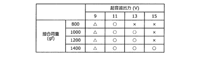
次に、ワイヤ7のワイヤボンディング条件について検証した。検証にはH&K社製ワイヤボンダBJ935(周波数60kHz)を使用した。図6,12は、実施の形態にかかる半導体装置のワイヤの接合強度を示す特性図である。図7は、従来の半導体装置のワイヤの接合強度を示す特性図である。異なるワイヤボンディング条件で複数の上記実施例1を作製し、ワイヤ7の接合強度を測定した結果を図6に示す。異なるワイヤボンディング条件で複数の上記実施例2を作製し、ワイヤ7の接合品質を測定した結果を図12に示す。比較として、実施例1,2と同様のワイヤボンディング条件で複数の上記従来例1を作製し、Alワイヤ107の接合強度を測定した結果を図7に示す。図6,12,7において、○はワイヤの接合強度が製品として耐え得る程度に十分に確保された場合を示し、△はワイヤの接合強度が低い場合を示し、×はワイヤが剥離して素子破壊に至った場合を示している(図13,14においても同様)。
Next, the wire bonding conditions of the
図6に示す結果より、実施例1においては、ワイヤボンディングの超音波出力を11V以上とした場合、ワイヤ7と被接合部材とを接合するための接合荷重を800gf〜1400gfとし、ワイヤボンディングの超音波出力を13V以上とした場合、接合荷重を1000gf〜1400gfとすることでワイヤ7の接合強度を十分に確保することができることが確認された。また、図12に示す結果より、実施例2においては、ワイヤボンディングの超音波出力を11V以上とすることで、ワイヤ7と被接合部材との接合強度を十分に確保することができる接合荷重範囲が広がり、接合荷重800gf〜1400gf内すべてにおいてワイヤ7と被接合部材との接合強度を十分に確保することができることが確認された。すなわち、Niめっき膜(おもて面金属膜14)の厚さを厚くすることにより、ワイヤ7と被接合部材との接合強度を十分に確保することができる接合荷重範囲が広がることがわかる。一方、図7に示す結果により、従来例1では、13V以上の高い超音波出力で、1400gf以上の高い接合荷重とした場合に、Alワイヤ107が剥離して素子破壊に至った。したがって、実施例1,2においては、従来例1よりも高い超音波出力および接合荷重とすることで、ワイヤ7の接合強度を正常な状態で確保することができることが確認された。
From the results shown in FIG. 6, in Example 1, when the ultrasonic output of wire bonding is 11 V or more, the bonding load for bonding the
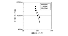
次に、実施の形態にかかる半導体装置のパワーサイクル耐量について検証した。図8は、実施の形態にかかる半導体装置のパワーサイクル耐量を示す特性図である。上述した実施例1,2および従来例1において、パワーサイクルの繰り返しサイクル数と、半導体素子の接合温度の温度変化ΔTjとの関係を図8に示す。半導体素子の接合温度の最大値Tjmaxを175℃とした。図8に示す結果より、実施例1,2は、高温での使用条件において、従来例1よりもパワーサイクルの繰り返しサイクルを多く行うことができることが確認された。すなわち、実施例1,2は、従来例1よりもパワーサイクル耐量を2倍以上に増加させることができた。 Next, the power cycle tolerance of the semiconductor device according to the embodiment was verified. FIG. 8 is a characteristic diagram showing the power cycle capability of the semiconductor device according to the embodiment. FIG. 8 shows the relationship between the number of cycles of the power cycle and the temperature change ΔTj of the junction temperature of the semiconductor element in Examples 1 and 2 and Conventional Example 1 described above. The maximum junction temperature Tjmax of the semiconductor element was 175 ° C. From the results shown in FIG. 8, it was confirmed that Examples 1 and 2 can perform more power cycle cycles than Conventional Example 1 under the use conditions at high temperatures. That is, Examples 1 and 2 were able to increase the power cycle tolerance twice or more than Conventional Example 1.
図9は、実施の形態にかかる半導体装置のワイヤボンディング後のワイヤの接合界面付近の状態を模式的に示す断面図である。図9(a)〜9(f)は、おもて面金属膜14として厚さ0.1μm、0.3μm、0.5μm、1μm、3μmおよび5μmのNiめっき膜を形成した半導体装置のワイヤ47の接合界面付近を示している。図9(a)〜図9(d)にはNiめっき膜43を線分で図示しており、この線分の太さでNiめっき膜43の膜厚を示している。図9(e),9(f)には、Niめっき膜44を黒く塗りつぶした横線で図示しており、この横線の太さ(半導体基板41の深さ方向の幅)でNiめっき膜44の膜厚を示している。
FIG. 9 is a cross-sectional view schematically showing a state in the vicinity of the bonding interface of the wire after the wire bonding of the semiconductor device according to the embodiment. 9A to 9F show wires of a semiconductor device in which Ni plating films having thicknesses of 0.1 μm, 0.3 μm, 0.5 μm, 1 μm, 3 μm, and 5 μm are formed as the front
厚さ0.3μmのNiめっき膜43を示す図9(b)は実施例1の半導体装置に対応し、厚さ5μmのNiめっき膜44を示す図9(f)は実施例2の半導体装置に対応する。図9(b)に示すように、厚さ0.3μmのNiめっき膜43を形成した実施例1では、Niめっき膜43がワイヤボンディングで破壊され、おもて面電極12であるAlSi電極42とワイヤ47との接合界面に分散していることが確認された。実施例1では、ワイヤ47の接合界面付近の状態が、ワイヤボンディング直後にNiめっき膜43が割れてワイヤ47とAlSi電極42とが直接接合し、微視的に図4(b)に示す参考例の態様となり、パワーサイクル試験後に図4(c)に示すようになっていることが確認された。図9(a),9(c),9(d)にそれぞれ示す厚さ0.1μm、0.5μmおよび1μmのNiめっき膜43を形成した半導体装置においても実施例1と同様にワイヤボンディング直後にNiめっき膜43が破壊されていた。
9B showing the
これに対して、図9(f),9(e)に示す厚さ5μmのNiめっき膜44を形成した実施例2、および厚さ3μmのNiめっき膜44を形成した半導体装置では、Niめっき膜44はワイヤボンディングで破壊されないことが確認された。このようにおもて面金属膜14の厚さを3μm以上、好ましくは3μm〜5μmとするのがよい。
On the other hand, in the second embodiment in which the
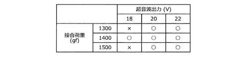
また、ワイヤ7のワイヤボンディング条件について、ワイヤ7の線径を500μmに太線化して検証した。図13は、実施の形態にかかる半導体装置の別の一例のワイヤの接合品質を示す特性図である。図14は、従来の半導体装置の別の一例のワイヤの接合品質を示す特性図である。○はワイヤの接合強度が製品として耐え得る程度に十分に確保された場合を示し、△はワイヤの接合強度が低い場合を示し、×はワイヤが剥離して素子破壊に至った場合を示している。異なるワイヤボンディング条件で、線径500μmのワイヤ7をおもて面金属膜14に接合した実施の形態にかかる半導体装置(以下、実施例3とする)において、ワイヤ7の接合強度を測定した結果を図13に示す。実施例3においては、おもて面金属膜14として厚さ5μmのNiめっき膜を形成した。実施例3の構成は、ワイヤ7の線径が異なることを除いて実施例2と同様である。また、比較として、異なるワイヤボンディング条件で、線径500μmのワイヤ37をおもて面電極112に接合した従来の半導体装置(以下、従来例2とする)において、ワイヤ37の接合強度を測定した結果を図14に示す。従来例2の構成は、ワイヤ37の線径が異なることを除いて参考例と同様である。
Further, the wire bonding conditions of the
図13に示す結果より、実施例3においては、Niめっき膜(おもて面金属膜14)の厚さを5.0μmとし、ワイヤ7の線径を500μmにすることで、ワイヤボンディングの超音波出力を高くし(18V〜22V)、かつワイヤ7と被接合部材とを接合するための接合荷重を大きくしたとしても(1300gf〜1500gf)、おもて面金属膜14とワイヤ7との接合部に接合不良が生じず、ワイヤ7の接合強度を十分に確保することができることが確認された。一方、図14に示す結果より、従来例2では、ワイヤ37の線径を500μmにした場合、ワイヤボンディングの超音波出力が低く(例えば18V)、ワイヤ37と被接合部材とを接合するための接合荷重が大きい(例えば1500gf)場合において、素子破壊が発生することが確認された。従来例2に生じた素子破壊は、今回の実験では超音波出力が低い(例えば18V)領域で素子破壊が発生したが、超音波接合の原理上、超音波出力が高い領域でも素子破壊は発生する虞がある。
From the results shown in FIG. 13, in Example 3, the thickness of the Ni plating film (front metal film 14) is set to 5.0 μm, and the wire diameter of the
以上、説明したように、実施の形態によれば、ワイヤの結晶粒径を制御して、ワイヤの再結晶温度を従来のアルミニウムワイヤの再結晶温度よりも高くし、かつワイヤの硬度をおもて面電極の硬度よりも高くすることで、従来よりも高温での使用条件においてもワイヤにクラックが生じることを抑制することができる。これにより、ワイヤにクラックが生じるまでの期間を従来よりも長くすることができる。また、実施の形態によれば、おもて面電極の表面にワイヤよりも硬度の高いおもて面金属膜を設けることで、おもて面電極を強化することができるため、おもて面電極にクラックが生じることを防止することができる。また、おもて面電極の表面にワイヤよりもさらに硬度の高いおもて面金属膜を設けることで、おもて面金属膜が障壁として機能するため、ワイヤにクラックが生じた場合でもこのクラックがおもて面電極に進展することを防止することができる。このように、おもて面電極にクラックを生じさせることなく、かつワイヤにクラックが生じることを抑制することができることで、パワーサイクル耐量を向上させることができる。したがって、信頼性の高い半導体装置を提供することができる。 As described above, according to the embodiment, the crystal grain size of the wire is controlled so that the recrystallization temperature of the wire is higher than the recrystallization temperature of the conventional aluminum wire, and the hardness of the wire is increased. By making it higher than the hardness of the surface electrode, it is possible to suppress the occurrence of cracks in the wire even under conditions of use at a higher temperature than before. Thereby, the period until a crack arises in a wire can be made longer than before. Moreover, according to the embodiment, the front electrode can be strengthened by providing the front metal film having a hardness higher than that of the wire on the surface of the front electrode. It can prevent that a crack arises in a surface electrode. Also, by providing a front surface metal film having a higher hardness than the wire on the surface of the front surface electrode, the front surface metal film functions as a barrier, so even if a crack occurs in the wire, It is possible to prevent the crack from progressing to the front electrode. As described above, the power cycle resistance can be improved by preventing the surface electrode from cracking and suppressing the cracking from occurring in the wire. Therefore, a highly reliable semiconductor device can be provided.
また、実施の形態によれば、ワイヤの硬度を高くすることで、ワイヤの熱変形によっておもて面電極にかかる応力が大きくなるが、おもて面電極の表面にワイヤよりも硬度の高いおもて面金属膜を設けることでおもて面電極が強化されるため、おもて面電極が破損することを防止することができる。 In addition, according to the embodiment, by increasing the hardness of the wire, the stress applied to the front electrode due to thermal deformation of the wire is increased, but the hardness of the surface of the front electrode is higher than that of the wire. Since the front electrode is strengthened by providing the front metal film, it is possible to prevent the front electrode from being damaged.
以上において本発明は種々変更可能であり、上述した各実施の形態において、例えば各部の寸法等は要求される仕様等に応じて種々設定される。 As described above, the present invention can be variously changed. In each of the above-described embodiments, for example, the dimensions and the like of each part are variously set according to required specifications.
以上のように、本発明にかかる半導体装置および半導体装置の製造方法は、汎用インバータや風力発電、太陽光発電、電鉄などに使用されるモジュール構造の半導体装置に有用である。 As described above, the semiconductor device and the method for manufacturing the semiconductor device according to the present invention are useful for a semiconductor device having a module structure used for a general-purpose inverter, wind power generation, solar power generation, electric railway, and the like.
1 半導体素子
1a はんだ接合層
2 絶縁基板
3 絶縁層
4 回路層
5 裏銅箔
6 Cuベース
7 ワイヤ
11 半導体基板
12 おもて面電極
13 裏面電極
14 おもて面金属膜
20 ワイヤの接合界面
21 クラックDESCRIPTION OF SYMBOLS 1 Semiconductor element 1a Solder bonding layer 2 Insulating substrate 3 Insulating layer 4 Circuit layer 5 Back copper foil 6
Claims (14)
前記電極の表面に、前記ワイヤよりも硬度が高い金属膜が設けられており、
前記ワイヤは、ワイヤボンディングによって前記金属膜に接合されており、
前記ワイヤの前記金属膜との接合界面の再結晶温度が175℃以上であり、
前記ワイヤの前記接合界面には、粒径が15μm以下の結晶粒のみを含み、
前記ワイヤの前記接合界面から離れた部分は、粒径が15μmより大きい結晶粒を含み、
前記半導体素子の接合温度は前記再結晶温度未満であることを特徴とする半導体装置。 In a semiconductor device formed by electrically connecting an electrode of a semiconductor element and a wire by wire bonding,
On the surface of the electrode, a metal film having a higher hardness than the wire is provided,
The wire is bonded to the metal film by wire bonding,
Ri der recrystallization temperature of 175 ° C. or more bonding interface between the metal film of the wire,
The bonding interface of the wire includes only crystal grains having a grain size of 15 μm or less,
The portion of the wire away from the bonding interface includes crystal grains having a grain size larger than 15 μm,
A semiconductor device, wherein a junction temperature of the semiconductor element is lower than the recrystallization temperature .
前記ワイヤよりも硬度が高い金属膜を前記電極の表面に設ける第1工程と、
ワイヤボンディング時に当該ワイヤボンディングの超音波振動により前記ワイヤの前記金属膜との接合界面の結晶粒を15μm以下の粒径の結晶粒のみにして前記ワイヤを前記金属膜に接合する第2工程と、
を含み、
前記第2工程では、前記ワイヤの前記接合界面から離れた部分の粒径を15μmより大きい結晶粒を含んだままの状態で維持し、
前記第2工程よりも後に行う工程では、前記半導体素子にかかる熱履歴の温度が、前記ワイヤの前記接合界面の再結晶温度未満であることを特徴とする半導体装置の製造方法。 In a method of manufacturing a semiconductor device for electrically connecting an electrode of a semiconductor element and a wire,
A first step of providing a metal film having a hardness higher than that of the wire on the surface of the electrode;
A second step of bonding the wire to the metal film by making only the crystal grains having a particle size of 15 μm or less at the bonding interface of the wire with ultrasonic vibration of the wire bonding at the time of wire bonding;
Including
In the second step, the particle diameter of the portion of the wire that is away from the bonding interface is maintained in a state in which crystal grains larger than 15 μm are included.
In the step performed after the second step, the temperature of the thermal history applied to the semiconductor element is lower than the recrystallization temperature of the bonding interface of the wire .
Applications Claiming Priority (3)
| Application Number | Priority Date | Filing Date | Title |
|---|---|---|---|
| JP2013092110 | 2013-04-25 | ||
| JP2013092110 | 2013-04-25 | ||
| PCT/JP2014/061457 WO2014175343A1 (en) | 2013-04-25 | 2014-04-23 | Semiconductor device and method for manufacturing semiconductor device |
Publications (2)
| Publication Number | Publication Date |
|---|---|
| JPWO2014175343A1 JPWO2014175343A1 (en) | 2017-02-23 |
| JP6132014B2 true JP6132014B2 (en) | 2017-05-24 |
Family
ID=51791911
Family Applications (1)
| Application Number | Title | Priority Date | Filing Date |
|---|---|---|---|
| JP2015513808A Active JP6132014B2 (en) | 2013-04-25 | 2014-04-23 | Semiconductor device and manufacturing method of semiconductor device |
Country Status (5)
| Country | Link |
|---|---|
| US (1) | US9748186B2 (en) |
| JP (1) | JP6132014B2 (en) |
| CN (1) | CN105190858B (en) |
| DE (1) | DE112014002135T5 (en) |
| WO (1) | WO2014175343A1 (en) |
Families Citing this family (15)
| Publication number | Priority date | Publication date | Assignee | Title |
|---|---|---|---|---|
| CN107210241B (en) * | 2015-03-10 | 2019-12-31 | 三菱电机株式会社 | Power semiconductor device |
| US10886250B2 (en) | 2015-07-10 | 2021-01-05 | Invensas Corporation | Structures and methods for low temperature bonding using nanoparticles |
| JP6665664B2 (en) * | 2016-04-27 | 2020-03-13 | 富士電機株式会社 | Semiconductor device and manufacturing method thereof |
| US10515913B2 (en) | 2017-03-17 | 2019-12-24 | Invensas Bonding Technologies, Inc. | Multi-metal contact structure |
| US10446441B2 (en) | 2017-06-05 | 2019-10-15 | Invensas Corporation | Flat metal features for microelectronics applications |
| US11152318B2 (en) * | 2017-11-22 | 2021-10-19 | Mitsubishi Electric Corporation | Semiconductor device and manufacturing method of semiconductor device |
| CN113611785B (en) * | 2018-02-01 | 2022-05-27 | 新唐科技日本株式会社 | Semiconductor device with a plurality of semiconductor chips |
| EP3550596A1 (en) * | 2018-04-04 | 2019-10-09 | Infineon Technologies AG | Arrangements and method for providing a wire bond connection |
| US10790262B2 (en) | 2018-04-11 | 2020-09-29 | Invensas Bonding Technologies, Inc. | Low temperature bonded structures |
| CN110158020B (en) * | 2019-04-09 | 2020-04-21 | 山东大学 | Method for preparing nano-structure oxide film by ultrasonic-assisted induction heating |
| WO2021236361A1 (en) | 2020-05-19 | 2021-11-25 | Invensas Bonding Technologies, Inc. | Laterally unconfined structure |
| CN112201628A (en) * | 2020-08-24 | 2021-01-08 | 株洲中车时代半导体有限公司 | Power module packaging structure and preparation method thereof |
| JP2024501559A (en) * | 2020-12-30 | 2024-01-12 | アデイア セミコンダクター ボンディング テクノロジーズ インコーポレイテッド | Structures with conductive features and methods of forming the same |
| WO2022163695A1 (en) * | 2021-01-28 | 2022-08-04 | 三菱電機株式会社 | Semiconductor device, power conversion device, and method for manufacturing semiconductor device |
| WO2024029286A1 (en) * | 2022-08-03 | 2024-02-08 | ローム株式会社 | Semiconductor device and method for manufacturing semiconductor device |
Family Cites Families (13)
| Publication number | Priority date | Publication date | Assignee | Title |
|---|---|---|---|---|
| JPS61163235A (en) | 1985-01-09 | 1986-07-23 | Toshiba Corp | Bonding wire for semiconductor device |
| JPS63148646A (en) * | 1986-12-12 | 1988-06-21 | Toshiba Corp | Semiconductor device |
| JPH07135234A (en) | 1993-11-09 | 1995-05-23 | Hitachi Ltd | Power semiconductor module |
| JPH088288A (en) | 1994-06-20 | 1996-01-12 | Hitachi Ltd | Semiconductor device |
| JPH08330710A (en) * | 1995-06-05 | 1996-12-13 | Nippon Paint Co Ltd | Metal plating working method for electrode portion of printed wiring board |
| JP2004200644A (en) * | 2002-10-22 | 2004-07-15 | Kyocera Corp | Wiring board |
| JP3918724B2 (en) * | 2002-11-28 | 2007-05-23 | トヨタ自動車株式会社 | Manufacturing method of semiconductor device in which wires are bonded |
| JP4696532B2 (en) * | 2004-05-20 | 2011-06-08 | 株式会社デンソー | Power composite integrated semiconductor device and manufacturing method thereof |
| JP2008311383A (en) | 2007-06-14 | 2008-12-25 | Ibaraki Univ | Bonding wire, bonding method using the same, and semiconductor device as well as joint construction |
| JP5214936B2 (en) * | 2007-09-21 | 2013-06-19 | 富士電機株式会社 | Semiconductor device |
| JP2010251483A (en) * | 2009-04-14 | 2010-11-04 | Renesas Electronics Corp | Semiconductor device and method of manufacturing the same |
| CN102244062B (en) * | 2011-07-26 | 2015-04-22 | 日月光半导体制造股份有限公司 | Semiconductor packaging structure and process |
| JP5159000B1 (en) * | 2012-06-13 | 2013-03-06 | 田中電子工業株式会社 | Aluminum alloy thin wires for connecting semiconductor devices |
-
2014
- 2014-04-23 WO PCT/JP2014/061457 patent/WO2014175343A1/en active Application Filing
- 2014-04-23 CN CN201480012154.0A patent/CN105190858B/en active Active
- 2014-04-23 DE DE112014002135.0T patent/DE112014002135T5/en active Pending
- 2014-04-23 JP JP2015513808A patent/JP6132014B2/en active Active
-
2015
- 2015-09-03 US US14/845,256 patent/US9748186B2/en active Active
Also Published As
| Publication number | Publication date |
|---|---|
| DE112014002135T5 (en) | 2016-01-14 |
| CN105190858A (en) | 2015-12-23 |
| JPWO2014175343A1 (en) | 2017-02-23 |
| WO2014175343A1 (en) | 2014-10-30 |
| US9748186B2 (en) | 2017-08-29 |
| US20150380368A1 (en) | 2015-12-31 |
| CN105190858B (en) | 2018-11-06 |
Similar Documents
| Publication | Publication Date | Title |
|---|---|---|
| JP6132014B2 (en) | Semiconductor device and manufacturing method of semiconductor device | |
| JP6895131B2 (en) | Solder material for semiconductor devices | |
| JP5159001B1 (en) | Aluminum alloy bonding wire | |
| WO2017217145A1 (en) | Solder bonded part | |
| JP6033011B2 (en) | Power semiconductor device and method for manufacturing power semiconductor device | |
| JP3988735B2 (en) | Semiconductor device and manufacturing method thereof | |
| JP5214936B2 (en) | Semiconductor device | |
| JP6056968B2 (en) | Semiconductor device | |
| KR20180091011A (en) | Copper ceramic substrate, a copper semi-finished product for manufacturing a copper ceramic substrate and a method for manufacturing a copper ceramic substrate | |
| JP6432465B2 (en) | Bonded body, power module substrate with heat sink, heat sink, method for manufacturing bonded body, method for manufacturing power module substrate with heat sink, and method for manufacturing heat sink | |
| TW201325330A (en) | Wiring substrate and method for manufacturing same and semiconductor device | |
| JP6575386B2 (en) | Manufacturing method of joined body, manufacturing method of power module substrate with heat sink, and manufacturing method of heat sink | |
| JP4544964B2 (en) | Heat dissipation board | |
| JPWO2016017679A1 (en) | Ceramic circuit board and manufacturing method thereof | |
| JP6440903B2 (en) | Semiconductor device and manufacturing method thereof | |
| WO2013005555A1 (en) | Metal-bonded structure and method for manufacturing same | |
| WO2013058020A1 (en) | Semiconductor device and semiconductor device manufacturing method | |
| JP2011061105A (en) | Connection structure, power module, and method of manufacturing the same | |
| JPH07169797A (en) | Method and structure for bonding | |
| JP2019114575A (en) | Semiconductor device and manufacturing method of the same | |
| JP4795471B2 (en) | Power semiconductor device | |
| JP2005032833A (en) | Module type semiconductor device | |
| JP2018125354A (en) | Semiconductor device | |
| JP2017059673A (en) | Cooler, power device, manufacturing method for cooler and manufacturing method for power device | |
| JP2017069366A (en) | Semiconductor device and method of manufacturing the same |
Legal Events
| Date | Code | Title | Description |
|---|---|---|---|
| A521 | Request for written amendment filed |
Free format text: JAPANESE INTERMEDIATE CODE: A523 Effective date: 20161107 |
|
| TRDD | Decision of grant or rejection written | ||
| A01 | Written decision to grant a patent or to grant a registration (utility model) |
Free format text: JAPANESE INTERMEDIATE CODE: A01 Effective date: 20170321 |
|
| A61 | First payment of annual fees (during grant procedure) |
Free format text: JAPANESE INTERMEDIATE CODE: A61 Effective date: 20170403 |
|
| R150 | Certificate of patent or registration of utility model |
Ref document number: 6132014 Country of ref document: JP Free format text: JAPANESE INTERMEDIATE CODE: R150 |
|
| R250 | Receipt of annual fees |
Free format text: JAPANESE INTERMEDIATE CODE: R250 |
|
| R250 | Receipt of annual fees |
Free format text: JAPANESE INTERMEDIATE CODE: R250 |
|
| R250 | Receipt of annual fees |
Free format text: JAPANESE INTERMEDIATE CODE: R250 |
|
| R250 | Receipt of annual fees |
Free format text: JAPANESE INTERMEDIATE CODE: R250 |
|
| R250 | Receipt of annual fees |
Free format text: JAPANESE INTERMEDIATE CODE: R250 |