JP6104575B2 - Semiconductor device - Google Patents
Semiconductor device Download PDFInfo
- Publication number
- JP6104575B2 JP6104575B2 JP2012260233A JP2012260233A JP6104575B2 JP 6104575 B2 JP6104575 B2 JP 6104575B2 JP 2012260233 A JP2012260233 A JP 2012260233A JP 2012260233 A JP2012260233 A JP 2012260233A JP 6104575 B2 JP6104575 B2 JP 6104575B2
- Authority
- JP
- Japan
- Prior art keywords
- semiconductor layer
- diamond semiconductor
- diamond
- plane
- plane orientation
- Prior art date
- Legal status (The legal status is an assumption and is not a legal conclusion. Google has not performed a legal analysis and makes no representation as to the accuracy of the status listed.)
- Active
Links
- 239000004065 semiconductor Substances 0.000 title claims description 484
- 229910003460 diamond Inorganic materials 0.000 claims description 419
- 239000010432 diamond Substances 0.000 claims description 419
- 239000012535 impurity Substances 0.000 claims description 124
- 239000000758 substrate Substances 0.000 claims description 48
- 239000010408 film Substances 0.000 description 67
- 238000001020 plasma etching Methods 0.000 description 32
- OAICVXFJPJFONN-UHFFFAOYSA-N Phosphorus Chemical compound [P] OAICVXFJPJFONN-UHFFFAOYSA-N 0.000 description 31
- 229910052698 phosphorus Inorganic materials 0.000 description 31
- 239000011574 phosphorus Substances 0.000 description 31
- 239000010936 titanium Substances 0.000 description 31
- 229910052751 metal Inorganic materials 0.000 description 30
- 239000002184 metal Substances 0.000 description 30
- 238000000034 method Methods 0.000 description 29
- 238000004519 manufacturing process Methods 0.000 description 22
- 238000010348 incorporation Methods 0.000 description 18
- 238000001459 lithography Methods 0.000 description 18
- 230000001681 protective effect Effects 0.000 description 18
- 238000005268 plasma chemical vapour deposition Methods 0.000 description 15
- RTAQQCXQSZGOHL-UHFFFAOYSA-N Titanium Chemical compound [Ti] RTAQQCXQSZGOHL-UHFFFAOYSA-N 0.000 description 14
- 230000015556 catabolic process Effects 0.000 description 14
- 229910052719 titanium Inorganic materials 0.000 description 14
- ZOXJGFHDIHLPTG-UHFFFAOYSA-N Boron Chemical compound [B] ZOXJGFHDIHLPTG-UHFFFAOYSA-N 0.000 description 13
- 229910052796 boron Inorganic materials 0.000 description 13
- PXHVJJICTQNCMI-UHFFFAOYSA-N Nickel Chemical compound [Ni] PXHVJJICTQNCMI-UHFFFAOYSA-N 0.000 description 10
- BASFCYQUMIYNBI-UHFFFAOYSA-N platinum Chemical compound [Pt] BASFCYQUMIYNBI-UHFFFAOYSA-N 0.000 description 9
- QVGXLLKOCUKJST-UHFFFAOYSA-N atomic oxygen Chemical compound [O] QVGXLLKOCUKJST-UHFFFAOYSA-N 0.000 description 7
- 239000010931 gold Substances 0.000 description 7
- 229910052760 oxygen Inorganic materials 0.000 description 7
- 239000001301 oxygen Substances 0.000 description 7
- 229910004298 SiO 2 Inorganic materials 0.000 description 6
- 230000005669 field effect Effects 0.000 description 6
- 238000000059 patterning Methods 0.000 description 6
- 238000001004 secondary ion mass spectrometry Methods 0.000 description 6
- 238000004544 sputter deposition Methods 0.000 description 5
- 229910052581 Si3N4 Inorganic materials 0.000 description 4
- VYPSYNLAJGMNEJ-UHFFFAOYSA-N Silicium dioxide Chemical compound O=[Si]=O VYPSYNLAJGMNEJ-UHFFFAOYSA-N 0.000 description 4
- 229910052759 nickel Inorganic materials 0.000 description 4
- HQVNEWCFYHHQES-UHFFFAOYSA-N silicon nitride Chemical compound N12[Si]34N5[Si]62N3[Si]51N64 HQVNEWCFYHHQES-UHFFFAOYSA-N 0.000 description 4
- 229910052814 silicon oxide Inorganic materials 0.000 description 4
- 238000001039 wet etching Methods 0.000 description 4
- DDFHBQSCUXNBSA-UHFFFAOYSA-N 5-(5-carboxythiophen-2-yl)thiophene-2-carboxylic acid Chemical compound S1C(C(=O)O)=CC=C1C1=CC=C(C(O)=O)S1 DDFHBQSCUXNBSA-UHFFFAOYSA-N 0.000 description 3
- 239000013078 crystal Substances 0.000 description 3
- 230000007547 defect Effects 0.000 description 3
- 238000001514 detection method Methods 0.000 description 3
- 230000006866 deterioration Effects 0.000 description 3
- 238000005566 electron beam evaporation Methods 0.000 description 3
- 239000000463 material Substances 0.000 description 3
- 239000010409 thin film Substances 0.000 description 3
- KJTLSVCANCCWHF-UHFFFAOYSA-N Ruthenium Chemical compound [Ru] KJTLSVCANCCWHF-UHFFFAOYSA-N 0.000 description 2
- 229910052782 aluminium Inorganic materials 0.000 description 2
- XAGFODPZIPBFFR-UHFFFAOYSA-N aluminium Chemical compound [Al] XAGFODPZIPBFFR-UHFFFAOYSA-N 0.000 description 2
- 238000005229 chemical vapour deposition Methods 0.000 description 2
- PCHJSUWPFVWCPO-UHFFFAOYSA-N gold Chemical compound [Au] PCHJSUWPFVWCPO-UHFFFAOYSA-N 0.000 description 2
- 229910052737 gold Inorganic materials 0.000 description 2
- BHEPBYXIRTUNPN-UHFFFAOYSA-N hydridophosphorus(.) (triplet) Chemical compound [PH] BHEPBYXIRTUNPN-UHFFFAOYSA-N 0.000 description 2
- 239000007769 metal material Substances 0.000 description 2
- 229910052697 platinum Inorganic materials 0.000 description 2
- 229910052707 ruthenium Inorganic materials 0.000 description 2
- WFKWXMTUELFFGS-UHFFFAOYSA-N tungsten Chemical compound [W] WFKWXMTUELFFGS-UHFFFAOYSA-N 0.000 description 2
- 229910052721 tungsten Inorganic materials 0.000 description 2
- 239000010937 tungsten Substances 0.000 description 2
- 230000004888 barrier function Effects 0.000 description 1
- 239000000969 carrier Substances 0.000 description 1
- 238000009792 diffusion process Methods 0.000 description 1
- 239000002019 doping agent Substances 0.000 description 1
- 239000012212 insulator Substances 0.000 description 1
- 238000005468 ion implantation Methods 0.000 description 1
- 230000005855 radiation Effects 0.000 description 1
- 239000007790 solid phase Substances 0.000 description 1
- 239000000126 substance Substances 0.000 description 1
Images


Classifications
-
- H—ELECTRICITY
- H01—ELECTRIC ELEMENTS
- H01L—SEMICONDUCTOR DEVICES NOT COVERED BY CLASS H10
- H01L29/00—Semiconductor devices specially adapted for rectifying, amplifying, oscillating or switching and having potential barriers; Capacitors or resistors having potential barriers, e.g. a PN-junction depletion layer or carrier concentration layer; Details of semiconductor bodies or of electrodes thereof ; Multistep manufacturing processes therefor
- H01L29/02—Semiconductor bodies ; Multistep manufacturing processes therefor
- H01L29/12—Semiconductor bodies ; Multistep manufacturing processes therefor characterised by the materials of which they are formed
- H01L29/16—Semiconductor bodies ; Multistep manufacturing processes therefor characterised by the materials of which they are formed including, apart from doping materials or other impurities, only elements of Group IV of the Periodic Table
- H01L29/1602—Diamond
-
- H—ELECTRICITY
- H01—ELECTRIC ELEMENTS
- H01L—SEMICONDUCTOR DEVICES NOT COVERED BY CLASS H10
- H01L21/00—Processes or apparatus adapted for the manufacture or treatment of semiconductor or solid state devices or of parts thereof
- H01L21/02—Manufacture or treatment of semiconductor devices or of parts thereof
- H01L21/02104—Forming layers
- H01L21/02365—Forming inorganic semiconducting materials on a substrate
- H01L21/02367—Substrates
- H01L21/0237—Materials
- H01L21/02373—Group 14 semiconducting materials
- H01L21/02376—Carbon, e.g. diamond-like carbon
-
- H—ELECTRICITY
- H01—ELECTRIC ELEMENTS
- H01L—SEMICONDUCTOR DEVICES NOT COVERED BY CLASS H10
- H01L21/00—Processes or apparatus adapted for the manufacture or treatment of semiconductor or solid state devices or of parts thereof
- H01L21/02—Manufacture or treatment of semiconductor devices or of parts thereof
- H01L21/02104—Forming layers
- H01L21/02365—Forming inorganic semiconducting materials on a substrate
- H01L21/02367—Substrates
- H01L21/02433—Crystal orientation
-
- H—ELECTRICITY
- H01—ELECTRIC ELEMENTS
- H01L—SEMICONDUCTOR DEVICES NOT COVERED BY CLASS H10
- H01L21/00—Processes or apparatus adapted for the manufacture or treatment of semiconductor or solid state devices or of parts thereof
- H01L21/02—Manufacture or treatment of semiconductor devices or of parts thereof
- H01L21/02104—Forming layers
- H01L21/02365—Forming inorganic semiconducting materials on a substrate
- H01L21/02436—Intermediate layers between substrates and deposited layers
- H01L21/02439—Materials
- H01L21/02441—Group 14 semiconducting materials
- H01L21/02444—Carbon, e.g. diamond-like carbon
-
- H—ELECTRICITY
- H01—ELECTRIC ELEMENTS
- H01L—SEMICONDUCTOR DEVICES NOT COVERED BY CLASS H10
- H01L21/00—Processes or apparatus adapted for the manufacture or treatment of semiconductor or solid state devices or of parts thereof
- H01L21/02—Manufacture or treatment of semiconductor devices or of parts thereof
- H01L21/02104—Forming layers
- H01L21/02365—Forming inorganic semiconducting materials on a substrate
- H01L21/02436—Intermediate layers between substrates and deposited layers
- H01L21/02494—Structure
- H01L21/02496—Layer structure
- H01L21/02502—Layer structure consisting of two layers
-
- H—ELECTRICITY
- H01—ELECTRIC ELEMENTS
- H01L—SEMICONDUCTOR DEVICES NOT COVERED BY CLASS H10
- H01L21/00—Processes or apparatus adapted for the manufacture or treatment of semiconductor or solid state devices or of parts thereof
- H01L21/02—Manufacture or treatment of semiconductor devices or of parts thereof
- H01L21/02104—Forming layers
- H01L21/02365—Forming inorganic semiconducting materials on a substrate
- H01L21/02436—Intermediate layers between substrates and deposited layers
- H01L21/02516—Crystal orientation
-
- H—ELECTRICITY
- H01—ELECTRIC ELEMENTS
- H01L—SEMICONDUCTOR DEVICES NOT COVERED BY CLASS H10
- H01L21/00—Processes or apparatus adapted for the manufacture or treatment of semiconductor or solid state devices or of parts thereof
- H01L21/02—Manufacture or treatment of semiconductor devices or of parts thereof
- H01L21/02104—Forming layers
- H01L21/02365—Forming inorganic semiconducting materials on a substrate
- H01L21/02518—Deposited layers
- H01L21/02521—Materials
- H01L21/02524—Group 14 semiconducting materials
- H01L21/02527—Carbon, e.g. diamond-like carbon
-
- H—ELECTRICITY
- H01—ELECTRIC ELEMENTS
- H01L—SEMICONDUCTOR DEVICES NOT COVERED BY CLASS H10
- H01L21/00—Processes or apparatus adapted for the manufacture or treatment of semiconductor or solid state devices or of parts thereof
- H01L21/02—Manufacture or treatment of semiconductor devices or of parts thereof
- H01L21/02104—Forming layers
- H01L21/02365—Forming inorganic semiconducting materials on a substrate
- H01L21/02518—Deposited layers
- H01L21/0257—Doping during depositing
- H01L21/02573—Conductivity type
- H01L21/02576—N-type
-
- H—ELECTRICITY
- H01—ELECTRIC ELEMENTS
- H01L—SEMICONDUCTOR DEVICES NOT COVERED BY CLASS H10
- H01L21/00—Processes or apparatus adapted for the manufacture or treatment of semiconductor or solid state devices or of parts thereof
- H01L21/02—Manufacture or treatment of semiconductor devices or of parts thereof
- H01L21/02104—Forming layers
- H01L21/02365—Forming inorganic semiconducting materials on a substrate
- H01L21/02518—Deposited layers
- H01L21/0257—Doping during depositing
- H01L21/02573—Conductivity type
- H01L21/02579—P-type
-
- H—ELECTRICITY
- H01—ELECTRIC ELEMENTS
- H01L—SEMICONDUCTOR DEVICES NOT COVERED BY CLASS H10
- H01L21/00—Processes or apparatus adapted for the manufacture or treatment of semiconductor or solid state devices or of parts thereof
- H01L21/02—Manufacture or treatment of semiconductor devices or of parts thereof
- H01L21/04—Manufacture or treatment of semiconductor devices or of parts thereof the devices having potential barriers, e.g. a PN junction, depletion layer or carrier concentration layer
- H01L21/0405—Manufacture or treatment of semiconductor devices or of parts thereof the devices having potential barriers, e.g. a PN junction, depletion layer or carrier concentration layer the devices having semiconductor bodies comprising semiconducting carbon, e.g. diamond, diamond-like carbon
- H01L21/041—Making n- or p-doped regions
-
- H—ELECTRICITY
- H01—ELECTRIC ELEMENTS
- H01L—SEMICONDUCTOR DEVICES NOT COVERED BY CLASS H10
- H01L21/00—Processes or apparatus adapted for the manufacture or treatment of semiconductor or solid state devices or of parts thereof
- H01L21/02—Manufacture or treatment of semiconductor devices or of parts thereof
- H01L21/04—Manufacture or treatment of semiconductor devices or of parts thereof the devices having potential barriers, e.g. a PN junction, depletion layer or carrier concentration layer
- H01L21/0405—Manufacture or treatment of semiconductor devices or of parts thereof the devices having potential barriers, e.g. a PN junction, depletion layer or carrier concentration layer the devices having semiconductor bodies comprising semiconducting carbon, e.g. diamond, diamond-like carbon
- H01L21/042—Changing their shape, e.g. forming recesses
-
- H—ELECTRICITY
- H01—ELECTRIC ELEMENTS
- H01L—SEMICONDUCTOR DEVICES NOT COVERED BY CLASS H10
- H01L29/00—Semiconductor devices specially adapted for rectifying, amplifying, oscillating or switching and having potential barriers; Capacitors or resistors having potential barriers, e.g. a PN-junction depletion layer or carrier concentration layer; Details of semiconductor bodies or of electrodes thereof ; Multistep manufacturing processes therefor
- H01L29/02—Semiconductor bodies ; Multistep manufacturing processes therefor
- H01L29/04—Semiconductor bodies ; Multistep manufacturing processes therefor characterised by their crystalline structure, e.g. polycrystalline, cubic or particular orientation of crystalline planes
- H01L29/045—Semiconductor bodies ; Multistep manufacturing processes therefor characterised by their crystalline structure, e.g. polycrystalline, cubic or particular orientation of crystalline planes by their particular orientation of crystalline planes
-
- H—ELECTRICITY
- H01—ELECTRIC ELEMENTS
- H01L—SEMICONDUCTOR DEVICES NOT COVERED BY CLASS H10
- H01L29/00—Semiconductor devices specially adapted for rectifying, amplifying, oscillating or switching and having potential barriers; Capacitors or resistors having potential barriers, e.g. a PN-junction depletion layer or carrier concentration layer; Details of semiconductor bodies or of electrodes thereof ; Multistep manufacturing processes therefor
- H01L29/02—Semiconductor bodies ; Multistep manufacturing processes therefor
- H01L29/06—Semiconductor bodies ; Multistep manufacturing processes therefor characterised by their shape; characterised by the shapes, relative sizes, or dispositions of the semiconductor regions ; characterised by the concentration or distribution of impurities within semiconductor regions
- H01L29/10—Semiconductor bodies ; Multistep manufacturing processes therefor characterised by their shape; characterised by the shapes, relative sizes, or dispositions of the semiconductor regions ; characterised by the concentration or distribution of impurities within semiconductor regions with semiconductor regions connected to an electrode not carrying current to be rectified, amplified or switched and such electrode being part of a semiconductor device which comprises three or more electrodes
- H01L29/1025—Channel region of field-effect devices
- H01L29/1029—Channel region of field-effect devices of field-effect transistors
- H01L29/1033—Channel region of field-effect devices of field-effect transistors with insulated gate, e.g. characterised by the length, the width, the geometric contour or the doping structure
- H01L29/1037—Channel region of field-effect devices of field-effect transistors with insulated gate, e.g. characterised by the length, the width, the geometric contour or the doping structure and non-planar channel
-
- H—ELECTRICITY
- H01—ELECTRIC ELEMENTS
- H01L—SEMICONDUCTOR DEVICES NOT COVERED BY CLASS H10
- H01L29/00—Semiconductor devices specially adapted for rectifying, amplifying, oscillating or switching and having potential barriers; Capacitors or resistors having potential barriers, e.g. a PN-junction depletion layer or carrier concentration layer; Details of semiconductor bodies or of electrodes thereof ; Multistep manufacturing processes therefor
- H01L29/02—Semiconductor bodies ; Multistep manufacturing processes therefor
- H01L29/36—Semiconductor bodies ; Multistep manufacturing processes therefor characterised by the concentration or distribution of impurities in the bulk material
-
- H—ELECTRICITY
- H01—ELECTRIC ELEMENTS
- H01L—SEMICONDUCTOR DEVICES NOT COVERED BY CLASS H10
- H01L29/00—Semiconductor devices specially adapted for rectifying, amplifying, oscillating or switching and having potential barriers; Capacitors or resistors having potential barriers, e.g. a PN-junction depletion layer or carrier concentration layer; Details of semiconductor bodies or of electrodes thereof ; Multistep manufacturing processes therefor
- H01L29/66—Types of semiconductor device ; Multistep manufacturing processes therefor
- H01L29/66007—Multistep manufacturing processes
- H01L29/66015—Multistep manufacturing processes of devices having a semiconductor body comprising semiconducting carbon, e.g. diamond, diamond-like carbon, graphene
- H01L29/66022—Multistep manufacturing processes of devices having a semiconductor body comprising semiconducting carbon, e.g. diamond, diamond-like carbon, graphene the devices being controllable only by variation of the electric current supplied or the electric potential applied, to one or more of the electrodes carrying the current to be rectified, amplified, oscillated or switched, e.g. two-terminal devices
- H01L29/6603—Diodes
-
- H—ELECTRICITY
- H01—ELECTRIC ELEMENTS
- H01L—SEMICONDUCTOR DEVICES NOT COVERED BY CLASS H10
- H01L29/00—Semiconductor devices specially adapted for rectifying, amplifying, oscillating or switching and having potential barriers; Capacitors or resistors having potential barriers, e.g. a PN-junction depletion layer or carrier concentration layer; Details of semiconductor bodies or of electrodes thereof ; Multistep manufacturing processes therefor
- H01L29/66—Types of semiconductor device ; Multistep manufacturing processes therefor
- H01L29/66007—Multistep manufacturing processes
- H01L29/66015—Multistep manufacturing processes of devices having a semiconductor body comprising semiconducting carbon, e.g. diamond, diamond-like carbon, graphene
- H01L29/66037—Multistep manufacturing processes of devices having a semiconductor body comprising semiconducting carbon, e.g. diamond, diamond-like carbon, graphene the devices being controllable only by the electric current supplied or the electric potential applied, to an electrode which does not carry the current to be rectified, amplified or switched, e.g. three-terminal devices
- H01L29/66045—Field-effect transistors
-
- H—ELECTRICITY
- H01—ELECTRIC ELEMENTS
- H01L—SEMICONDUCTOR DEVICES NOT COVERED BY CLASS H10
- H01L29/00—Semiconductor devices specially adapted for rectifying, amplifying, oscillating or switching and having potential barriers; Capacitors or resistors having potential barriers, e.g. a PN-junction depletion layer or carrier concentration layer; Details of semiconductor bodies or of electrodes thereof ; Multistep manufacturing processes therefor
- H01L29/66—Types of semiconductor device ; Multistep manufacturing processes therefor
- H01L29/68—Types of semiconductor device ; Multistep manufacturing processes therefor controllable by only the electric current supplied, or only the electric potential applied, to an electrode which does not carry the current to be rectified, amplified or switched
- H01L29/76—Unipolar devices, e.g. field effect transistors
- H01L29/772—Field effect transistors
- H01L29/78—Field effect transistors with field effect produced by an insulated gate
-
- H—ELECTRICITY
- H01—ELECTRIC ELEMENTS
- H01L—SEMICONDUCTOR DEVICES NOT COVERED BY CLASS H10
- H01L29/00—Semiconductor devices specially adapted for rectifying, amplifying, oscillating or switching and having potential barriers; Capacitors or resistors having potential barriers, e.g. a PN-junction depletion layer or carrier concentration layer; Details of semiconductor bodies or of electrodes thereof ; Multistep manufacturing processes therefor
- H01L29/66—Types of semiconductor device ; Multistep manufacturing processes therefor
- H01L29/68—Types of semiconductor device ; Multistep manufacturing processes therefor controllable by only the electric current supplied, or only the electric potential applied, to an electrode which does not carry the current to be rectified, amplified or switched
- H01L29/76—Unipolar devices, e.g. field effect transistors
- H01L29/772—Field effect transistors
- H01L29/80—Field effect transistors with field effect produced by a PN or other rectifying junction gate, i.e. potential-jump barrier
- H01L29/812—Field effect transistors with field effect produced by a PN or other rectifying junction gate, i.e. potential-jump barrier with a Schottky gate
- H01L29/8128—Field effect transistors with field effect produced by a PN or other rectifying junction gate, i.e. potential-jump barrier with a Schottky gate with recessed gate
-
- H—ELECTRICITY
- H01—ELECTRIC ELEMENTS
- H01L—SEMICONDUCTOR DEVICES NOT COVERED BY CLASS H10
- H01L29/00—Semiconductor devices specially adapted for rectifying, amplifying, oscillating or switching and having potential barriers; Capacitors or resistors having potential barriers, e.g. a PN-junction depletion layer or carrier concentration layer; Details of semiconductor bodies or of electrodes thereof ; Multistep manufacturing processes therefor
- H01L29/66—Types of semiconductor device ; Multistep manufacturing processes therefor
- H01L29/86—Types of semiconductor device ; Multistep manufacturing processes therefor controllable only by variation of the electric current supplied, or only the electric potential applied, to one or more of the electrodes carrying the current to be rectified, amplified, oscillated or switched
- H01L29/861—Diodes
- H01L29/868—PIN diodes
-
- H—ELECTRICITY
- H01—ELECTRIC ELEMENTS
- H01L—SEMICONDUCTOR DEVICES NOT COVERED BY CLASS H10
- H01L29/00—Semiconductor devices specially adapted for rectifying, amplifying, oscillating or switching and having potential barriers; Capacitors or resistors having potential barriers, e.g. a PN-junction depletion layer or carrier concentration layer; Details of semiconductor bodies or of electrodes thereof ; Multistep manufacturing processes therefor
- H01L29/66—Types of semiconductor device ; Multistep manufacturing processes therefor
- H01L29/86—Types of semiconductor device ; Multistep manufacturing processes therefor controllable only by variation of the electric current supplied, or only the electric potential applied, to one or more of the electrodes carrying the current to be rectified, amplified, oscillated or switched
- H01L29/861—Diodes
- H01L29/872—Schottky diodes
-
- H—ELECTRICITY
- H01—ELECTRIC ELEMENTS
- H01L—SEMICONDUCTOR DEVICES NOT COVERED BY CLASS H10
- H01L29/00—Semiconductor devices specially adapted for rectifying, amplifying, oscillating or switching and having potential barriers; Capacitors or resistors having potential barriers, e.g. a PN-junction depletion layer or carrier concentration layer; Details of semiconductor bodies or of electrodes thereof ; Multistep manufacturing processes therefor
- H01L29/02—Semiconductor bodies ; Multistep manufacturing processes therefor
- H01L29/06—Semiconductor bodies ; Multistep manufacturing processes therefor characterised by their shape; characterised by the shapes, relative sizes, or dispositions of the semiconductor regions ; characterised by the concentration or distribution of impurities within semiconductor regions
- H01L29/0657—Semiconductor bodies ; Multistep manufacturing processes therefor characterised by their shape; characterised by the shapes, relative sizes, or dispositions of the semiconductor regions ; characterised by the concentration or distribution of impurities within semiconductor regions characterised by the shape of the body
-
- H—ELECTRICITY
- H01—ELECTRIC ELEMENTS
- H01L—SEMICONDUCTOR DEVICES NOT COVERED BY CLASS H10
- H01L29/00—Semiconductor devices specially adapted for rectifying, amplifying, oscillating or switching and having potential barriers; Capacitors or resistors having potential barriers, e.g. a PN-junction depletion layer or carrier concentration layer; Details of semiconductor bodies or of electrodes thereof ; Multistep manufacturing processes therefor
- H01L29/40—Electrodes ; Multistep manufacturing processes therefor
- H01L29/41—Electrodes ; Multistep manufacturing processes therefor characterised by their shape, relative sizes or dispositions
- H01L29/423—Electrodes ; Multistep manufacturing processes therefor characterised by their shape, relative sizes or dispositions not carrying the current to be rectified, amplified or switched
- H01L29/42312—Gate electrodes for field effect devices
- H01L29/42316—Gate electrodes for field effect devices for field-effect transistors
- H01L29/4232—Gate electrodes for field effect devices for field-effect transistors with insulated gate
- H01L29/42356—Disposition, e.g. buried gate electrode
- H01L29/4236—Disposition, e.g. buried gate electrode within a trench, e.g. trench gate electrode, groove gate electrode
Landscapes
- Engineering & Computer Science (AREA)
- Microelectronics & Electronic Packaging (AREA)
- Power Engineering (AREA)
- Computer Hardware Design (AREA)
- Physics & Mathematics (AREA)
- Condensed Matter Physics & Semiconductors (AREA)
- General Physics & Mathematics (AREA)
- Manufacturing & Machinery (AREA)
- Ceramic Engineering (AREA)
- Chemical & Material Sciences (AREA)
- Crystallography & Structural Chemistry (AREA)
- Materials Engineering (AREA)
- Electrodes Of Semiconductors (AREA)
- Junction Field-Effect Transistors (AREA)
- Insulated Gate Type Field-Effect Transistor (AREA)
Description
本発明の実施の形態は半導体装置に関する。 Embodiments described herein relate generally to a semiconductor device.
ダイヤモンドはその機械的、化学的および熱的特性に加え、優れた半導体特性を持つことから、半導体デバイス材料として注目されている。特に、室温で約5.5eVのバンドギャップを持つため、紫外線発光デバイスや負性電子親和力を利用した電子放出デバイスとして期待される。また、絶縁破壊耐性が高いため、パワーデバイスとしても期待される。さらに、堅牢な結晶性から、特に高温や放射線などの過酷な環境下で用いられる耐環境性デバイスとして期待される。 Diamond has attracted attention as a semiconductor device material because of its excellent semiconductor properties in addition to its mechanical, chemical and thermal properties. In particular, since it has a band gap of about 5.5 eV at room temperature, it is expected as an ultraviolet light emitting device or an electron emitting device utilizing negative electron affinity. In addition, since it has high dielectric breakdown resistance, it is also expected as a power device. Furthermore, it is expected as an environment-resistant device that is used under severe environments such as high temperature and radiation due to its robust crystallinity.
ダイヤモンドのパワーデバイスは近年盛んに開発が行われ、ショットキー接合を有するショットキーバリアダイオード、pin構造のデバイス、ショットキー接合にpn接合を組み合わせたデバイス、等に関する報告がなされている。 Diamond power devices have been actively developed in recent years, and reports have been made on Schottky barrier diodes having a Schottky junction, devices having a pin structure, devices in which a pn junction is combined with a Schottky junction, and the like.
また、ダイヤモンド半導体層形成時の不純物の取り込み効率は、下地層の面方位に強く依存することが知られている。 Further, it is known that the efficiency of impurity incorporation when forming the diamond semiconductor layer strongly depends on the plane orientation of the underlayer.
本発明は、上記事情を考慮してなされたものであり、その目的とするところは、不純物濃度が制御されたダイヤモンド半導体層を備え、低オン抵抗で高耐圧の半導体装置を提供することにある。 The present invention has been made in view of the above circumstances, and an object of the present invention is to provide a semiconductor device having a diamond semiconductor layer with a controlled impurity concentration and having a low on-resistance and a high breakdown voltage. .
実施の形態の半導体装置は、主面が{111}面から<011>方向に45度以下の傾斜を有する面方位である第1導電型の第1のダイヤモンド半導体層と、前記第1のダイヤモンド半導体層に形成されるトレンチ構造と、前記トレンチ構造内の前記第1のダイヤモンド半導体層上に形成され、前記第1のダイヤモンド半導体層より低不純物濃度の第2のダイヤモンド半導体層と、前記第2のダイヤモンド半導体層上に形成され、前記第2のダイヤモンド半導体層よりも高不純物濃度の第2導電型の第3のダイヤモンド半導体層と、前記第1のダイヤモンド半導体層に電気的に接続される第1の電極と、前記第3のダイヤモンド半導体層に電気的に接続される第2の電極と、を備え、前記第1のダイヤモンド半導体層と前記第2のダイヤモンド半導体層の界面の面方位が{100}面または{110}面から±10度以内の面方位であることを特徴とする。
The semiconductor device according to the embodiment includes a first conductivity type first diamond semiconductor layer whose principal surface has a plane orientation with an inclination of 45 degrees or less in the <011> direction from the {111} plane , and the first diamond A trench structure formed in the semiconductor layer; a second diamond semiconductor layer formed on the first diamond semiconductor layer in the trench structure and having a lower impurity concentration than the first diamond semiconductor layer; and the second A third diamond semiconductor layer of a second conductivity type having a higher impurity concentration than that of the second diamond semiconductor layer and electrically connected to the first diamond semiconductor layer. a first electrode, said third and second electrodes electrically connected to the diamond semiconductor layer, wherein the said first diamond semiconductor layer and the second diamond The plane orientation of the interface of the semiconductor layer has a plane orientation der Rukoto of ± 10 degrees from the {100} plane or the {110} plane.
ダイヤモンド半導体では、不純物のドーピングをイオン注入や固相拡散で行うことは困難であり、通常、半導体層成膜時にドーピングを行う方法が採用される。 In a diamond semiconductor, it is difficult to perform impurity doping by ion implantation or solid phase diffusion, and a method of doping at the time of forming a semiconductor layer is usually employed.
そして、ダイヤモンド半導体の成膜時には、不純物取り込み効率の面方位依存性が顕著である。このため、半導体ダイヤモンド層形成の際に、下地層に含有される不純物によるオートドーピングの程度にも面方位依存性が顕著に現れる。 When the diamond semiconductor is formed, the dependency of the impurity incorporation efficiency on the plane orientation is remarkable. For this reason, when the semiconductor diamond layer is formed, the plane orientation dependency is remarkably exhibited in the degree of auto-doping due to impurities contained in the underlayer.
本発明の実施の形態では、ダイヤモンド半導体を材料とする半導体装置を形成する際に、トレンチ構造を用いることで、異なる半導体層を異なる面方位で形成可能とする。これにより、ダイヤモンド半導体に取り込まれる不純物濃度を制御する。したがって、ダイヤモンド半導体層内の不純物濃度を所望の値に精度高く制御することが可能である。特に、半導体装置の特性を大きく作用する真性あるいは低濃度不純物層の不純物濃度の制御性が向上し、安定して低オン抵抗で高耐圧の半導体装置が実現される。 In the embodiment of the present invention, when a semiconductor device made of a diamond semiconductor is formed, a different semiconductor layer can be formed with different plane orientations by using a trench structure. Thereby, the impurity concentration taken into the diamond semiconductor is controlled. Therefore, the impurity concentration in the diamond semiconductor layer can be controlled to a desired value with high accuracy. In particular, the controllability of the intrinsic or low-concentration impurity layer, which greatly affects the characteristics of the semiconductor device, is improved, and a semiconductor device with low on-resistance and high breakdown voltage can be realized stably.
以下、図面を参照しつつ本発明の実施の形態を説明する。 Hereinafter, embodiments of the present invention will be described with reference to the drawings.
(第1の実施の形態)
本実施の形態の半導体装置は、主面が第1の面方位を有する第1導電型の第1のダイヤモンド半導体層と、第1のダイヤモンド半導体層に形成されるトレンチ構造と、トレンチ構造内の第1のダイヤモンド半導体層上に形成され、第1のダイヤモンド半導体層より低不純物濃度の第2のダイヤモンド半導体層と、第2のダイヤモンド半導体層上に形成され、第2のダイヤモンド半導体層よりも高不純物濃度の第2導電型の第3のダイヤモンド層と、第1のダイヤモンド半導体層に電気的に接続される第1の電極と、第3のダイヤモンド半導体層に電気的に接続される第2の電極と、を備える。
(First embodiment)
The semiconductor device of the present embodiment includes a first conductivity type first diamond semiconductor layer having a main surface having a first plane orientation, a trench structure formed in the first diamond semiconductor layer, A second diamond semiconductor layer formed on the first diamond semiconductor layer and having a lower impurity concentration than the first diamond semiconductor layer, and formed on the second diamond semiconductor layer and higher than the second diamond semiconductor layer. A third diamond layer of the second conductivity type having an impurity concentration, a first electrode electrically connected to the first diamond semiconductor layer, and a second electrode electrically connected to the third diamond semiconductor layer An electrode.
本実施の形態の半導体装置は、上記構成を備えることにより、特に、真性半導体または低不純物濃度の第2のダイヤモンド半導体層の不純物が精度良く制御される。したがって、安定した特性を備える低オン抵抗で高耐圧の半導体装置を実現することが可能となる。 The semiconductor device according to the present embodiment has the above-described structure, and in particular, the impurities of the intrinsic semiconductor or the second diamond semiconductor layer having a low impurity concentration are controlled with high accuracy. Therefore, it is possible to realize a semiconductor device having stable characteristics and low on-resistance and high breakdown voltage.
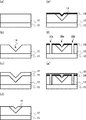
図1は、本実施の形態の半導体装置の模式断面図である。本実施の形態の半導体装置100は、トレンチ型のpinダイオードである。
FIG. 1 is a schematic cross-sectional view of the semiconductor device of the present embodiment. The
半導体装置100は、例えば、主面が第1の面方位を備える単結晶ダイヤモンドの基板10上に形成される。第1の面方位は、例えば、{111}面から<011>方向に45度以下の傾斜を備える面方位である。ここで、主面とは、基板10の最も広い面を意味し、基板10がウェハであれば、ウェハの表面および裏面を意味する。
The
基板10上に、主面が第1の面方位を有するn型の第1のダイヤモンド半導体層12が形成される。第1の面方位は、例えば、{111}面から0度から10度のオフ角を備える面方位である。
An n-type first
第1のダイヤモンド半導体層12の不純物濃度は、例えば、1×10¹⁸atoms/cm3以上1×1021atoms/cm3以下である。n型不純物は、例えば、リン(P)である。
The impurity concentration of the first
そして、第1のダイヤモンド半導体層12にトレンチ構造14が形成される。トレンチ構造14は、例えば、断面がV字形状を備える。そして、トレンチ構造14は、第1の面方位と異なる第2の面方位、例えば、{100}面または{110}面が、トレンチ内面に形成されるように設けられている。
Then, a
そして、トレンチ構造14内の第1のダイヤモンド半導体層12上に、第2のダイヤモンド半導体層16が形成される。第2のダイヤモンド半導体層16は、いわゆるドリフト層である。
Then, a second
第2のダイヤモンド半導体層16は、第1のダイヤモンド半導体層12より低不純物濃度である。第2のダイヤモンド半導体層16は、例えば、n型、p型または真性半導体であるi(intrinsic)型である。第2のダイヤモンド半導体層16の不純物濃度は、1×10¹⁵atoms/cm3以下であることが高耐圧および高移動度を実現する観点から望ましい。
The second
そして、第2のダイヤモンド半導体層16上に、p型の第3のダイヤモンド半導体層18が形成される。第3のダイヤモンド半導体層18は、第2のダイヤモンド半導体層16よりも高不純物濃度である。
Then, a p-type third
第3のダイヤモンド半導体層18の不純物濃度は、例えば、1×10¹⁸atoms/cm3以上1×1021atoms/cm3以下である。p型不純物は、例えば、ボロン(B)である。
The impurity concentration of the third
さらに、第1のダイヤモンド半導体層12に電気的に接続される第1の電極20を備えている。第1の電極20は、カソード(陰極)である。
Furthermore, a
第1の電極20は、第1のダイヤモンド半導体層12に設けられた溝内に形成される。この構造により、第1のダイヤモンド半導体層12との接触面積を増大させ、コンタクト抵抗を低減している。
The
第1の電極20は、金属で形成される。金属は、例えば、チタン(Ti)である。第1の電極20と第1のダイヤモンド半導体層12との間は、オーミックコンタクトであることが望ましい。
The
また、第3のダイヤモンド半導体層18に電気的に接続される第2の電極22を備えている。第2の電極22は、アノード(陽極)である。
A
第2の電極22は、金属で形成される。金属は、例えば、チタン(Ti)である。第2の電極22と第3のダイヤモンド半導体層18との間は、オーミックコンタクトであることが望ましい。
The
第1のダイヤモンド半導体層12、第2のダイヤモンド半導体層16、第3のダイヤモンド半導体層18の表面には、絶縁膜24が形成されている。絶縁膜24上には、第1の電極20および第2の電極22の一部が形成されている。
An insulating
本実施の形態では、{111}面近傍の面方位を備えるn型の第1のダイヤモンド半導体層12上に、ドリフト層となる第2のダイヤモンド半導体層16を形成する。この際、第1のダイヤモンド半導体層12に形成したトレンチ構造14内に第2のダイヤモンド半導体層16を形成する。トレンチ構造14は、{111}面と面方位の異なる第2の面、例えば、{100}面または{110}面が、トレンチ内面に形成されるように設けられる。
In the present embodiment, second
CVD(Chemical Vapor Deposition)成長によって形成されるダイヤモンド半導体層では、不純物の層内への取り込み効率は、面方位に強く依存する。例えば、不純物がn型ドーパントであるリン(P)の場合、{111}面基板上の{111}面成長の場合、すなわち<111>方向への成長の場合、リンの取り込み効率は0.02%程度である。 In a diamond semiconductor layer formed by CVD (Chemical Vapor Deposition) growth, the efficiency of impurity incorporation into the layer strongly depends on the plane orientation. For example, when the impurity is phosphorus (P) which is an n-type dopant, in the case of {111} plane growth on a {111} plane substrate, that is, in the case of growth in the <111> direction, the phosphorus incorporation efficiency is 0.02 %.
これに対し、{110}面基板上の{110}面成長の場合、すなわち<110>方向への成長の場合、リンの取り込み効率は0.0002%程度である。また、{100}面基板上の{100}面成長の場合、すなわち<100>方向への成長の場合、リンの取り込み効率は0.00001%未満である。 On the other hand, in the case of {110} plane growth on the {110} plane substrate, that is, in the <110> direction, the phosphorus incorporation efficiency is about 0.0002%. Further, in the case of {100} plane growth on a {100} plane substrate, that is, in the <100> direction, the phosphorus incorporation efficiency is less than 0.00001%.
そして、ボロン(B)についても、リン(P)と同様の傾向があり、{111}面基板上の<111>方向の{111}面成長の場合に取り込み効率が高くなる。 Boron (B) also has the same tendency as phosphorus (P), and the incorporation efficiency increases in the case of {111} plane growth in the <111> direction on the {111} plane substrate.
このため、ダイヤモンド半導体層を形成する際の下地層に、高濃度の不純物が含有されていると、下地由来の不純物の取り込み、いわゆる、オートドーピングが生じ、不純物濃度の安定した制御が困難となる。特に真性半導体や低濃度のダイヤモンド半導体層を形成する際、この問題は顕著となる。 For this reason, when a high concentration of impurities is contained in the underlayer when forming the diamond semiconductor layer, the incorporation of impurities derived from the underlayer, so-called auto-doping occurs, making it difficult to stably control the impurity concentration. . This problem is particularly noticeable when an intrinsic semiconductor or a low-concentration diamond semiconductor layer is formed.
本実施の形態の半導体装置100の構成によれば、第1のダイヤモンド半導体層12は{111}面近傍の面方位を備えることで、n型不純物のリンを高濃度に含有させることが容易となる。第1のダイヤモンド半導体層12は、第1の電極20とのコンタクト層として、コンタクト抵抗とオン抵抗とを低くするため不純物濃度が高濃度であることが要求される。
According to the configuration of the
一方、ドリフト層である第2のダイヤモンド半導体層16は、薄膜で高耐圧とするために、低不純物濃度であることが要求される。本実施の形態の半導体装置100の構成によれば、高不純物濃度の第1のダイヤモンド半導体層12にトレンチ構造を設け、{100}面、{110}面等、{111}面と面方位の異なる面を下地として、第2のダイヤモンド半導体層16を成長させることが可能になる。
On the other hand, the second
したがって、第1のダイヤモンド半導体層12由来の不純物の取り込みが抑制され、安定して不純物濃度を低濃度に制御することが可能となる。よって、例えば、オン抵抗が0.1mΩcm2以下、と低オン抵抗で、例えば、耐圧が1kV以上、と高耐圧のpinダイオードを再現性良く安定して製造することが可能となる。
Accordingly, the incorporation of impurities derived from the first
また、不純物の取り込みが抑制されることで、接合界面の急峻性の劣化や欠陥の発生を抑制することが可能となる。よって、キャリア移動度の低下や逆方向のリーク電流の増大も抑制することが可能となる。 In addition, by suppressing the incorporation of impurities, it is possible to suppress the deterioration of the steepness of the bonding interface and the generation of defects. Therefore, it is possible to suppress a decrease in carrier mobility and an increase in reverse leakage current.
なお、第1のダイヤモンド半導体層12への不純物取り込み効率を大きくする観点から、第1の面方位が{111}面から<011>方向に45度以下の傾斜を有する面方位であることが望ましく、第1の面方位が{111}面から<011>方向に30度以下の傾斜を有する面方位であることがより望ましく、第1の面方位が{111}面から<011>方向に15度以下の傾斜を有する面方位であることがさらに望ましい。
Note that, from the viewpoint of increasing the efficiency of impurity incorporation into the first
また、第2のダイヤモンド半導体層16への不純物の取り込みを抑制する観点から、第1のダイヤモンド半導体層12と第2のダイヤモンド半導体層16の界面の面方位が{100}面または{110}面から±10度以内の面方位であることが望ましく、±5度以内の面方位であることがより望ましい。
Further, from the viewpoint of suppressing the incorporation of impurities into the second
また、トレンチ構造14については、V字形状である場合を例に説明したが、内面に第1の面方位以外の、第2の面方位を備える構造であれば、V字形状に限らず、例えば、U字形状、矩形形状等であってもかまわない。また、第2のダイヤモンド半導体層16は、トレンチ構造14の内面の全領域に形成されていなくとも、一部の領域に形成されるものであってもかまわない。
In addition, the
次に、本実施の形態の半導体装置の製造方法について説明する。本実施の形態の半導体装置の製造方法は、主面が第1の面方位を備える基板を準備し、基板上に主面が第1の面方位を備える第1導電型の第1のダイヤモンド半導体層を形成し、第1のダイヤモンド半導体層にトレンチ構造を形成し、トレンチ構造内の第1のダイヤモンド半導体層上に、第1のダイヤモンド半導体層より低不純物濃度の第2のダイヤモンド半導体層を形成し、第2のダイヤモンド半導体層上に、第2のダイヤモンド半導体層よりも高不純物濃度の第2導電型の第3のダイヤモンド半導体層を形成し、第1のダイヤモンド半導体層に電気的に接続される第1の電極を形成し、第3のダイヤモンド半導体層に電気的に接続される第2の電極を形成する。 Next, a method for manufacturing the semiconductor device of the present embodiment will be described. The method for manufacturing a semiconductor device according to the present embodiment provides a substrate having a main surface having a first surface orientation, and a first conductivity type first diamond semiconductor having a main surface having a first surface orientation on the substrate. Forming a trench structure in the first diamond semiconductor layer, and forming a second diamond semiconductor layer having a lower impurity concentration than the first diamond semiconductor layer on the first diamond semiconductor layer in the trench structure. A second conductivity type third diamond semiconductor layer having a higher impurity concentration than the second diamond semiconductor layer is formed on the second diamond semiconductor layer, and is electrically connected to the first diamond semiconductor layer. The first electrode is formed, and the second electrode electrically connected to the third diamond semiconductor layer is formed.
図2(a)〜(g)は、本実施の形態の半導体装置の製造方法を示す模式断面図である。 2A to 2G are schematic cross-sectional views illustrating the method for manufacturing the semiconductor device of the present embodiment.
まず、主面が第1の面方位を備える基板10を準備する。基板10は、例えば、ノンドープのダイヤモンド半導体である。第1の面方位は、例えば{111}である。
First, the
そして、基板10上に、主面が、例えば{111}の面方位を備えるn型の第1のダイヤモンド半導体層12を形成する(図2(a))。第1のダイヤモンド半導体層12には不純物としてリン(P)が含まれる。第1のダイヤモンド半導体層12の不純物濃度は、例えば、1×10¹⁸atoms/cm3以上1×1021atoms/cm3以下である。第1のダイヤモンド半導体層12は、例えば、マイクロ波プラズマCVD法で形成する。
Then, an n-type first
なお、第1のダイヤモンド半導体層12に不純物を高濃度に含有させる観点から、第1の面方位が{111}面から<011>方向に45度以下の傾斜を有する面方位であることが望ましい。
From the viewpoint of containing impurities in the first
次に、第1のダイヤモンド半導体層12に、例えば、リソグラフィー法とRIE(Reactive Ion Etching)法を用いて、トレンチ構造14を形成する(図2(b))。トレンチ構造14は、例えば、V字型である。V字型のトレンチ構造14の内面は、第1の面方位と異なる第2の面方位を備える。第2の面方位は、例えば、{110}である。
Next, the
次に、トレンチ構造14内の第1のダイヤモンド半導体層12上に、第1のダイヤモンド半導体層12より低不純物濃度の第2のダイヤモンド半導体層16を形成する。第2のダイヤモンド半導体層16は、例えば、不純物を積極的に導入しないノンドープのダイヤモンド半導体層である。トレンチ構造内14では、内面に露出する第2の面方位、例えば、{110}、と同じ面方位の第2のダイヤモンド半導体層16が形成される。すなわち、第2のダイヤモンド半導体層16は、<110>方向に成長する。第2のダイヤモンド半導体層16は、例えば、マイクロ波プラズマCVD法で形成する。
Next, a second
<110>方向に{110}面方位で成長する場合、<111>方向に{111}面方位で成長する場合に比較して、リン(P)の取り込み効率は小さい。したがって、第2のダイヤモンド半導体層16形成の際に、下地のリンを高濃度に含有する第1のダイヤモンド半導体層12からの、リンのオートドーピングが抑制される。したがって、極めて真性半導体に近い第2のダイヤモンド半導体層16を形成することが可能となる。
When growing in the {110} plane orientation in the <110> direction, the phosphorus (P) uptake efficiency is lower than in the case of growing in the {111} plane orientation in the <111> direction. Therefore, when the second
なお、ここでは、第2の面方位が{110}である場合を例に説明したが、第2の面方位は、第1面方位と異なる面方位であれば、これに限定されるものではない。第2の面方位は、第2のダイヤモンド半導体層16への不純物のオートドーピングを抑制する観点から、{100}面または{110}面から±10度以内の面方位であることが望ましい。
In addition, although the case where the second plane orientation is {110} has been described as an example here, the second plane orientation is not limited to this as long as the second plane orientation is different from the first plane orientation. Absent. The second plane orientation is preferably a plane orientation within ± 10 degrees from the {100} plane or {110} plane from the viewpoint of suppressing the impurity auto-doping into the second
次に、第2のダイヤモンド半導体層16上に、第2のダイヤモンド半導体層16よりも高不純物濃度のp型の第3のダイヤモンド半導体層18を形成する(図2(c))。第3のダイヤモンド半導体層18には不純物としてボロン(B)が含まれる。第3のダイヤモンド半導体層18の不純物濃度は、例えば、1×10¹⁸atoms/cm3以上1×1021atoms/cm3以下である。第3のダイヤモンド半導体層18は、例えば、マイクロ波プラズマCVD法で形成する。
Next, a p-type third
次に、第3のダイヤモンド半導体層18上のトレンチ構造14内の斜面を含む領域に、保護膜(図示せず)を形成する。保護膜は、例えば、シリコン酸化膜である。
Next, a protective film (not shown) is formed in a region including the slope in the
その後、例えば、酸素系のRIEにより、第2のダイヤモンド半導体層16および第3のダイヤモンド半導体層18を、第1のダイヤモンド半導体層12が表面に露出するまでエッチングする。その後、保護膜はウェットエッチング等により除去する(図2(d))。
Thereafter, the second
次に、第3のダイヤモンド半導体層18上のトレンチ構造14内の斜面を含む領域に、絶縁膜24を形成する(図2(e))。絶縁膜24は、例えば、シリコン窒化膜である。
Next, an insulating
次に、例えば、リソグラフィー法とRIE法により、絶縁膜24に開口部30a、30bを形成する。そして、開口部30a、30bに、例えば、RIE法により、例えば、基板10に達する溝を形成する。また、例えば、リソグラフィー法とRIE法により、絶縁膜24に開口部30cを形成する(図2(f))。
Next,
その後、金属膜32、例えば、チタン(Ti)膜を、スパッタ法により形成する(図2(g))。
Thereafter, a
その後、例えば、リソグラフィー法とRIE法により、金属膜32をパターニングし、第1の電極20および第2の電極22を形成する。以上の製造方法により、図1に示す半導体装置100が形成される。
Thereafter, the
(第2の実施の形態)
本実施の形態の半導体装置は、主面が第1の面方位を有する第1導電型の第1のダイヤモンド半導体層と、第1のダイヤモンド半導体層に形成されるトレンチ構造と、トレンチ構造内の第1のダイヤモンド半導体層上に形成され、第1のダイヤモンド半導体層より低不純物濃度の第2のダイヤモンド半導体層と、第1のダイヤモンド半導体層に電気的に接続される第1の電極と、第2のダイヤモンド半導体層に電気的に接続される第2の電極と、
を備える。
(Second Embodiment)
The semiconductor device of the present embodiment includes a first conductivity type first diamond semiconductor layer having a main surface having a first plane orientation, a trench structure formed in the first diamond semiconductor layer, A second diamond semiconductor layer formed on the first diamond semiconductor layer and having a lower impurity concentration than the first diamond semiconductor layer; a first electrode electrically connected to the first diamond semiconductor layer; A second electrode electrically connected to the two diamond semiconductor layers;
Is provided.
本実施の形態の半導体装置は、第3のダイヤモンド半導体層を備えない、ショットキーダイオードである点で、第1の実施の形態と異なっている。第1の実施の形態と重複する内容については記載を省略する。 The semiconductor device of this embodiment is different from that of the first embodiment in that it is a Schottky diode that does not include the third diamond semiconductor layer. The description overlapping with the first embodiment is omitted.
図3は、本実施の形態の半導体装置の模式断面図である。本実施の形態の半導体装置200は、トレンチ型のショットキーダイオードである。
FIG. 3 is a schematic cross-sectional view of the semiconductor device of the present embodiment. The
半導体装置200は、例えば、主面が第1の面方位を備える単結晶ダイヤモンドの基板10上に形成される。第1の面方位は、例えば、{111}面から<011>方向に45度以下の傾斜を備える面方位である。
The
基板10上に、主面が第1の面方位を有するn型の第1のダイヤモンド半導体層12が形成される。第1の面方位は、例えば、{111}面から0度から10度のオフ角を備える面方位である。
An n-type first
第1のダイヤモンド半導体層12の不純物濃度は、例えば、1×10¹⁸atoms/cm3以上1×1021atoms/cm3以下である。n型不純物は、例えば、リン(P)である。
The impurity concentration of the first
そして、第1のダイヤモンド半導体層12にトレンチ構造14が形成される。トレンチ構造14は、例えば、断面がV字形状を備える。そして、トレンチ構造14は、第1の面方位と異なる第2の面方位、例えば、{100}面または{110}面が、トレンチ内面に形成されるように設けられている。
Then, a
そして、トレンチ構造14内の第1のダイヤモンド半導体層12上に、第2のダイヤモンド半導体層16が形成される。第2のダイヤモンド半導体層16は、いわゆるドリフト層である。
Then, a second
第2のダイヤモンド半導体層16は、第1のダイヤモンド半導体層12より低不純物濃度である。第2のダイヤモンド半導体層16は、例えば、n型、p型または真性半導体であるi(intrinsic)型である。第2のダイヤモンド半導体層16の不純物濃度は、1×10¹⁵atoms/cm3以下であることが高耐圧を実現する観点から望ましい。
The second
さらに、第1のダイヤモンド半導体層12に電気的に接続される第1の電極20を備えている。第1の電極20は、カソード(陰極)である。
Furthermore, a
第1の電極20は、第1のダイヤモンド半導体層12に設けられた溝内に形成される。この構造により、第1のダイヤモンド半導体層12との接触面積を増大させ、コンタクト抵抗を低減している。
The
第1の電極20は、金属で形成される。金属は、例えば、チタン(Ti)である。第1の電極20と第1のダイヤモンド半導体層12との間は、オーミックコンタクトであることが望ましい。
The
また、第2のダイヤモンド半導体層16に電気的に接続される第2の電極22を備えている。第2の電極22は、アノード(陽極)である。
A
第2の電極22は、金属で形成される。金属は、例えば、ニッケル(Ni)である。第2の電極22と第2のダイヤモンド半導体層16との間は、ショットキー接合である。第2の電極22の金属は、第2のダイヤモンド半導体層16とショットキー接合を形成する材料であれば、ニッケルに限定されることなく、例えば、アルミニウム(Al)、金(Au)、白金(Pt)、ルテニウム(Ru)、チタン(Ti)、タングステン(W)を適用することも可能である。
The
第1のダイヤモンド半導体層12、第2のダイヤモンド半導体層16の表面には、絶縁膜24が形成されている。絶縁膜24上には、第1の電極20および第2の電極22の一部が形成されている。
An insulating
本実施の形態の半導体装置200の構成によれば、第1のダイヤモンド半導体層12は{111}面近傍の面方位を備えることで、n型不純物のリンを高濃度に含有させることが容易となる。第1のダイヤモンド半導体層12は、第1の電極20とのコンタクト層として、コンタクト抵抗とオン抵抗とを低くするため不純物濃度が高濃度であることが要求される。
According to the configuration of the
そして、ドリフト層である第2のダイヤモンド半導体層16は、薄膜で高耐圧とするために、低不純物濃度であることが要求される。本実施の形態の半導体装置100の構成によれば、高不純物濃度の第1のダイヤモンド半導体層12にトレンチ構造を設け、{100}面、{110}面等、{111}面と面方位の異なる面を下地として、第2のダイヤモンド半導体層16を成長させることが可能になる。
The second
したがって、第1のダイヤモンド半導体層12由来の不純物の取り込みが抑制され、安定して不純物濃度を低濃度に制御することが可能となる。よって、例えば、オン抵抗が0.1mΩcm2以下、と低オン抵抗で、例えば、耐圧が1kV以上、と高耐圧のショットキーダイオードを再現性良く安定して製造することが可能となる。
Accordingly, the incorporation of impurities derived from the first
また、不純物の取り込みが抑制されることで、接合界面の急峻性の劣化や欠陥の発生を抑制することが可能となる。よって、キャリア移動度の低下や逆方向のリーク電流の増大も抑制することが可能となる。 In addition, by suppressing the incorporation of impurities, it is possible to suppress the deterioration of the steepness of the bonding interface and the generation of defects. Therefore, it is possible to suppress a decrease in carrier mobility and an increase in reverse leakage current.
次に、本実施の形態の半導体装置の製造方法について説明する。本実施の形態の半導体装置の製造方法は、主面が第1の面方位を備える基板を準備し、基板上に主面が第1の面方位を備える第1導電型の第1のダイヤモンド半導体層を形成し、第1のダイヤモンド半導体層にトレンチ構造を形成し、トレンチ構造内の第1のダイヤモンド半導体層上に、第1のダイヤモンド半導体層より低不純物濃度の第2のダイヤモンド半導体層を形成し、第1のダイヤモンド半導体層に電気的に接続される第1の電極を形成し、第2のダイヤモンド半導体層に電気的に接続される第2の電極を形成する。 Next, a method for manufacturing the semiconductor device of the present embodiment will be described. The method for manufacturing a semiconductor device according to the present embodiment provides a substrate having a main surface having a first surface orientation, and a first conductivity type first diamond semiconductor having a main surface having a first surface orientation on the substrate. Forming a trench structure in the first diamond semiconductor layer, and forming a second diamond semiconductor layer having a lower impurity concentration than the first diamond semiconductor layer on the first diamond semiconductor layer in the trench structure. Then, a first electrode electrically connected to the first diamond semiconductor layer is formed, and a second electrode electrically connected to the second diamond semiconductor layer is formed.
図4(a)〜(g)は、本実施の形態の半導体装置の製造方法を示す模式断面図である。 4A to 4G are schematic cross-sectional views illustrating the method for manufacturing the semiconductor device of the present embodiment.
まず、主面が第1の面方位を備える基板10を準備する。基板10は、例えば、ノンドープのダイヤモンド半導体である。第1の面方位は、例えば{111}である。
First, the
そして、基板10上に、主面が、例えば{111}の面方位を備えるn型の第1のダイヤモンド半導体層12を形成する(図4(a))。第1のダイヤモンド半導体層12には不純物としてリン(P)が含まれる。第1のダイヤモンド半導体層12の不純物濃度は、例えば、1×10¹⁸atoms/cm3以上1×1021atoms/cm3以下である。第1のダイヤモンド半導体層12は、例えば、マイクロ波プラズマCVD法で形成する。
Then, an n-type first
なお、第1のダイヤモンド半導体層12に不純物を高濃度に含有させる観点から、第1の面方位が{111}面から<011>方向に45度以下の傾斜を有する面方位であることが望ましい。
From the viewpoint of containing impurities in the first
次に、第1のダイヤモンド半導体層12に、例えば、リソグラフィー法とRIE(Reactive Ion Etching)法を用いて、トレンチ構造14を形成する(図4(b))。トレンチ構造14は、例えば、断面がV字形状である。V字形状のトレンチ構造14の内面は、第1の面方位と異なる第2の面方位を備える。第2の面方位は、例えば、{110}である。
Next, the
次に、トレンチ構造14内の第1のダイヤモンド半導体層12上に、第1のダイヤモンド半導体層12より低不純物濃度の第2のダイヤモンド半導体層16を形成する(図4(c))。第2のダイヤモンド半導体層16は、例えば、不純物を積極的に導入しないノンドープのダイヤモンド半導体層である。トレンチ構造内14では、内面に露出する第2の面方位、例えば、{110}、と同じ面方位の第2のダイヤモンド半導体層16が形成される。第2のダイヤモンド半導体層16は、<110>方向に成長して形成される。第2のダイヤモンド半導体層16は、例えば、マイクロ波プラズマCVD法で形成する。
Next, a second
<110>方向に{110}面方位で成長する場合、<111>方向に{111}面方位で成長する場合に比較して、リン(P)の取り込み効率は小さい。したがって、第2のダイヤモンド半導体層16形成の際に、下地のリンを高濃度に含有する第1のダイヤモンド半導体層12からの、リンのオートドーピングが抑制される。したがって、極めて真性半導体に近い第2のダイヤモンド半導体層16を形成することが可能となる。
When growing in the {110} plane orientation in the <110> direction, the phosphorus (P) uptake efficiency is lower than in the case of growing in the {111} plane orientation in the <111> direction. Therefore, when the second
なお、ここでは、第2の面方位が{110}である場合を例に説明したが、第2の面方位は、第1の面方位と異なる面方位であれば、これに限定されるものではない。第2の面方位は、第2のダイヤモンド半導体層16への不純物のオートドーピングを抑制する観点から、{100}面または{110}面から±10度以内の面方位であることが望ましい。
Here, the case where the second plane orientation is {110} has been described as an example, but the second plane orientation is limited to this as long as the second plane orientation is different from the first plane orientation. is not. The second plane orientation is preferably a plane orientation within ± 10 degrees from the {100} plane or {110} plane from the viewpoint of suppressing the impurity auto-doping into the second
次に、第2のダイヤモンド半導体層16上のトレンチ構造14内の斜面を含む領域に、保護膜(図示せず)を形成する。保護膜は、例えば、シリコン酸化膜である。
Next, a protective film (not shown) is formed in a region including the slope in the
その後、例えば、酸素系のRIEにより、第2のダイヤモンド半導体層16を、第1のダイヤモンド半導体層12が表面に露出するまでエッチングする。その後、保護膜はウェットエッチング等により除去する(図4(d))。
Thereafter, the second
次に、第3のダイヤモンド半導体層18上のトレンチ構造14内の斜面を含む領域に、絶縁膜24を形成する(図4(e))。絶縁膜24は、例えば、シリコン窒化膜である。
Next, an insulating
次に、例えば、リソグラフィー法とRIE法により、絶縁膜24に開口部30a、30bを形成する。そして、開口部30a、30bに、例えば、RIE法により、例えば、基板10に達する溝を形成する。また、例えば、リソグラフィー法とRIE法により、絶縁膜24に開口部30cを形成する(図4(f))。
Next,
その後、金属膜32、例えば、チタン(Ti)膜を、スパッタ法により形成する(図4(g))。
Thereafter, a
その後、例えば、リソグラフィー法とRIE法により、金属膜32をパターニングし、第1の電極20および第2の電極22を形成する。以上の製造方法により、図3に示す半導体装置200が形成される。
Thereafter, the
なお、第1の電極20と第2の第2の電極22とに、異なる金属材料を適用してもかまわない。
Note that different metal materials may be applied to the
(第3の実施の形態)
本実施の形態の半導体装置は、基板と、基板上に形成され、主面が第1の面方位を有する第1導電型の第1のダイヤモンド半導体層と、第1のダイヤモンド半導体層に形成され、最深部が基板に達し、第1のダイヤモンド半導体層を第1の領域と第2の領域に分離するトレンチ構造と、トレンチ構造内の第1のダイヤモンド半導体層上に形成され、第1のダイヤモンド半導体層より低不純物濃度の第2のダイヤモンド半導体層と、第1の領域に電気的に接続されるソース電極と、第2の領域に電気的に接続されるドレイン電極と、第2のダイヤモンド半導体層上に形成されるゲート電極と、を備える。
(Third embodiment)
The semiconductor device of the present embodiment is formed on a substrate, a first conductivity type first diamond semiconductor layer formed on the substrate, and having a main surface having a first plane orientation, and the first diamond semiconductor layer. A deepest portion reaches the substrate, and a first diamond semiconductor layer is formed on the first diamond semiconductor layer in the trench structure, the trench structure separating the first diamond semiconductor layer into the first region and the second region; A second diamond semiconductor layer having a lower impurity concentration than the semiconductor layer; a source electrode electrically connected to the first region; a drain electrode electrically connected to the second region; and a second diamond semiconductor A gate electrode formed on the layer.
本実施の形態の半導体装置は、ダイオードではなく電界効果トランジスタである点で、第1および第2の実施の形態と異なる。第1または第2の実施の形態と重複する内容については記載を省略する。 The semiconductor device of this embodiment is different from the first and second embodiments in that it is a field effect transistor instead of a diode. The description overlapping with the first or second embodiment is omitted.
図5は、本実施の形態の半導体装置の模式断面図である。本実施の形態の半導体装置300は、トレンチ型の電界効果トランジスタである。
FIG. 5 is a schematic cross-sectional view of the semiconductor device of the present embodiment. The
半導体装置300は、例えば、主面が第1の面方位を備える単結晶ダイヤモンドの基板10上に形成される。第1の面方位は、例えば、{111}面から<011>方向に45度以下の傾斜を備える面方位である。
The
基板10上に、主面が第1の面方位を有するn型の第1のダイヤモンド半導体層12が形成される。第1の面方位は、例えば、{111}面から0度から10度のオフ角を備える面方位である。
An n-type first
第1のダイヤモンド半導体層12の不純物濃度は、例えば、1×10¹⁸atoms/cm3以上1×1021atoms/cm3以下である。n型不純物は、例えば、リン(P)である。
The impurity concentration of the first
そして、第1のダイヤモンド半導体層12にトレンチ構造14が形成される。トレンチ構造14は、例えば、断面がV字形状を備える。トレンチ構造14により、第1のダイヤモンド半導体層12がソース領域(第1の領域)12aとドレイン領域(第2の領域)12bに分離される。そして、トレンチ構造14は、第1の面方位と異なる第2の面方位、例えば、{100}面または{110}面が、トレンチ内面に形成されるように設けられている。
Then, a
そして、トレンチ構造14内の第1のダイヤモンド半導体層12上に、第2のダイヤモンド半導体層16が形成される。第2のダイヤモンド半導体層16は、キャリアが伝導される、いわゆるチャネル層である。
Then, a second
第2のダイヤモンド半導体層16は、第1のダイヤモンド半導体層12より低不純物濃度である。第2のダイヤモンド半導体層16は、例えば、n型、p型または真性半導体であるi(intrinsic)型である。第2のダイヤモンド半導体層16の不純物濃度は、1×10¹⁵atoms/cm3以下であることが適切な閾値設定の観点から望ましい。
The second
さらに、第1のダイヤモンド半導体層12の第1の領域12aに電気的に接続されるソース電極40を備えている。ソース電極40は、例えば、第1のダイヤモンド半導体層12の第1の領域12aに設けられた溝内に形成される。この構造により、第1のダイヤモンド半導体層12との接触面積を増大させ、コンタクト抵抗を低減している。
Further, a
ソース電極40は、金属で形成される。金属は、例えば、チタン(Ti)である。ソース電極40と第1のダイヤモンド半導体層12との間は、オーミックコンタクトであることが望ましい。
The
また、第1のダイヤモンド半導体層12の第2の領域12bに電気的に接続されるドレイン電極42を備えている。ドレイン電極42は、例えば、第1のダイヤモンド半導体層12の第2の領域12bに設けられた溝内に形成される。この構造により、第1のダイヤモンド半導体層12との接触面積を増大させ、コンタクト抵抗を低減している。
In addition, a
ドレイン電極42は、金属で形成される。金属は、例えば、チタン(Ti)である。ドレイン電極42と第1のダイヤモンド半導体層12との間は、オーミックコンタクトであることが望ましい。
The
また、第2のダイヤモンド半導体層16に電気的に接続されるゲート電極44を備えている。ゲート電極44は、金属で形成される。金属は、例えば、ニッケル(Ni)である。ゲート電極44と第2のダイヤモンド半導体層16との間は、ショットキー接合である。ゲート電極44の金属は、第2のダイヤモンド半導体層16とショットキー接合を形成する材料であれば、ニッケルに限定されることなく、例えば、アルミニウム(Al)、金(Au)、白金(Pt)、ルテニウム(Ru)、チタン(Ti)、タングステン(W)を適用することも可能である。
Further, a
第1のダイヤモンド半導体層12、第2のダイヤモンド半導体層16の表面には、絶縁膜24が形成されている。絶縁膜24上には、ソース電極40、ドレイン電極42およびゲート電極44の一部が形成されている。
An insulating
本実施の形態の半導体装置300の構成によれば、第1のダイヤモンド半導体層12は{111}面近傍の面方位を備えることで、n型不純物のリンを高濃度に含有させることが容易となる。第1のダイヤモンド半導体層12は、ソース電極40、ドレイン電極42とのコンタクト層として、コンタクト抵抗とオン抵抗とを低くするため不純物濃度が高濃度であることが要求される。
According to the configuration of the
そして、チャネル層である第2のダイヤモンド半導体層16は、薄膜で高耐圧とするために、低不純物濃度であることが要求される。本実施の形態の半導体装置100の構成によれば、高不純物濃度の第1のダイヤモンド半導体層12にトレンチ構造を設け、{100}面、{110}面等、{111}面と面方位の異なる面を下地として、第2のダイヤモンド半導体層16を成長させることが可能になる。よって、第1のダイヤモンド半導体層12由来の不純物の取り込みが抑制され、安定して不純物濃度を低濃度に制御することが可能となる。よって、オン抵抗が低く、高耐圧の電界効果トランジスタを再現性良く安定して製造することが可能となる。
The second
また、不純物の取り込みが抑制されることで、接合界面の急峻性の劣化や欠陥の発生を抑制することが可能となる。よって、キャリア移動度の低下やリーク電流の増大も抑制することが可能となる。 In addition, by suppressing the incorporation of impurities, it is possible to suppress the deterioration of the steepness of the bonding interface and the generation of defects. Therefore, it is possible to suppress a decrease in carrier mobility and an increase in leakage current.
なお、第2のダイヤモンド半導体層16とゲート電極44との間にゲート絶縁膜を設け、MISFET(Metal Insulator Semiconductor Fieled Effect Transistor)構造を採用することも可能である。
It is also possible to provide a gate insulating film between the second
次に、本実施の形態の半導体装置の製造方法について説明する。本実施の形態の半導体装置の製造方法は、主面が第1の面方位を備える基板を準備し、基板上に主面が第1の面方位を備える第1導電型の第1のダイヤモンド半導体層を形成し、第1のダイヤモンド半導体層に、最深部が基板に達するトレンチ構造を形成し、トレンチ構造内の第1のダイヤモンド半導体層上に、第1のダイヤモンド半導体層より低不純物濃度の第2のダイヤモンド半導体層を形成し、第1のダイヤモンド半導体層に電気的に接続されるソース電極およびドレイン電極を形成し、第2のダイヤモンド半導体層に電気的に接続されるゲート電極を形成する。 Next, a method for manufacturing the semiconductor device of the present embodiment will be described. The method for manufacturing a semiconductor device according to the present embodiment provides a substrate having a main surface having a first surface orientation, and a first conductivity type first diamond semiconductor having a main surface having a first surface orientation on the substrate. Forming a trench structure having a deepest portion reaching the substrate in the first diamond semiconductor layer, and having a lower impurity concentration than the first diamond semiconductor layer on the first diamond semiconductor layer in the trench structure; Two diamond semiconductor layers are formed, a source electrode and a drain electrode electrically connected to the first diamond semiconductor layer are formed, and a gate electrode electrically connected to the second diamond semiconductor layer is formed.
図6(a)〜(g)は、本実施の形態の半導体装置の製造方法を示す模式断面図である。 6A to 6G are schematic cross-sectional views illustrating the method for manufacturing the semiconductor device of the present embodiment.
まず、主面が第1の面方位を備える基板10を準備する。基板10は、例えば、ノンドープのダイヤモンド半導体である。第1の面方位は、例えば{111}である。
First, the
そして、基板10上に、主面が、例えば{111}の面方位を備えるn型の第1のダイヤモンド半導体層12を形成する(図6(a))。第1のダイヤモンド半導体層12には不純物としてリン(P)が含まれる。第1のダイヤモンド半導体層12の不純物濃度は、例えば、1×10¹⁸atoms/cm3以上1×1021atoms/cm3以下である。第1のダイヤモンド半導体層12は、例えば、マイクロ波プラズマCVD法で形成する。
Then, an n-type first
なお、第1のダイヤモンド半導体層12に不純物を高濃度に含有させる観点から、第1の面方位が{111}面から<011>方向に45度以下の傾斜を有する面方位であることが望ましい。
From the viewpoint of containing impurities in the first
次に、第1のダイヤモンド半導体層12に、例えば、リソグラフィー法とRIE(Reactive Ion Etching)法を用いて、最深部が基板10に達するトレンチ構造14を形成する(図6(b))。トレンチ構造14は、例えば、V字型である。V字型のトレンチ構造14の内面は、第1の面方位と異なる第2の面方位を備える。第2の面方位は、例えば、{110}である。
Next, a
次に、トレンチ構造14内の第1のダイヤモンド半導体層12上に、第1のダイヤモンド半導体層12より低不純物濃度の第2のダイヤモンド半導体層16を形成する(図6(c))。第2のダイヤモンド半導体層16は、例えば、不純物を積極的に導入しないノンドープの真性ダイヤモンド半導体層である。トレンチ構造内14では、内面に露出する第2の面方位、例えば、{110}、と同じ面方位の第2のダイヤモンド半導体層16が形成される。すなわち、第2のダイヤモンド半導体層16は、<110>方向に成長して形成される。第2のダイヤモンド半導体層16は、例えば、マイクロ波プラズマCVD法で形成する。
Next, a second
<110>方向に{110}面方位で成長する場合、<111>方向に{111}面方位で成長する場合に比較して、リン(P)の取り込み効率は小さい。したがって、第2のダイヤモンド半導体層16形成の際に、下地のリンを高濃度に含有する第1のダイヤモンド半導体層12からのオートドーピングが抑制される。したがって、極めて真性半導体に近い第2のダイヤモンド半導体層16を形成することが可能となる。
When growing in the {110} plane orientation in the <110> direction, the phosphorus (P) uptake efficiency is lower than in the case of growing in the {111} plane orientation in the <111> direction. Therefore, when the second
なお、ここでは、第2の面方位が{110}である場合を例に説明したが、第2の面方位は、これに限定されるものではない。例えば、第2の面方位は、第2のダイヤモンド半導体層16への不純物のオートドーピングを抑制する観点から、{100}面または{110}面から±10度以内の面方位であることが望ましい。
Here, the case where the second plane orientation is {110} has been described as an example, but the second plane orientation is not limited to this. For example, the second plane orientation is preferably a plane orientation within ± 10 degrees from the {100} plane or {110} plane from the viewpoint of suppressing the autodoping of impurities into the second
次に、第2のダイヤモンド半導体層16上のトレンチ構造14内の斜面を含む領域に、保護膜(図示せず)を形成する。保護膜は、例えば、シリコン酸化膜である。
Next, a protective film (not shown) is formed in a region including the slope in the
その後、例えば、酸素系のRIEにより、第2のダイヤモンド半導体層16を、第1のダイヤモンド半導体層12が表面に露出するまでエッチングする。その後、保護膜はウェットエッチング等により除去する(図6(d))。
Thereafter, the second
次に、第3のダイヤモンド半導体層18上のトレンチ構造14内の斜面を含む領域に、絶縁膜24を形成する(図6(e))。絶縁膜24は、例えば、シリコン窒化膜である。
Next, an insulating
次に、例えば、リソグラフィー法とRIE法により、絶縁膜24に開口部30a、30bを形成する。そして、開口部30a、30bに、例えば、RIE法により、例えば、基板10に達する溝を形成する。また、例えば、リソグラフィー法とRIE法により、絶縁膜24に開口部30cを形成する(図6(f))。
Next,
その後、金属膜32、例えば、チタン(Ti)膜を、スパッタ法により形成する(図6(g))。
Thereafter, a
その後、例えば、リソグラフィー法とRIE法により、金属膜32をパターニングし、ソース電極40、ドレイン電極42およびゲート電極44を形成する。以上の製造方法により、図5に示す半導体装置300が形成される。
Thereafter, for example, the
なお、ソース電極40、ドレイン電極42とゲート電極44とに異なる金属材料を適用してもかまわない。
Note that different metal materials may be applied to the
(第4の実施の形態) (Fourth embodiment)
本実施の形態の半導体装置は、主面が第1の面方位を有する第1導電型の第1のダイヤモンド半導体層と、第1のダイヤモンド半導体層上に形成され、第1のダイヤモンド半導体層より低不純物濃度の第2のダイヤモンド半導体層と、第2のダイヤモンド半導体層に形成されるトレンチ構造と、トレンチ構造内の第2のダイヤモンド半導体層上に形成され、第2のダイヤモンド半導体層より高不純物濃度の第3のダイヤモンド半導体層と、第1のダイヤモンド半導体層に電気的に接続される第1の電極と、第3のダイヤモンド半導体層に電気的に接続される第2の電極と、を備える。 The semiconductor device of the present embodiment is formed on a first conductivity type first diamond semiconductor layer having a main surface having a first plane orientation, and the first diamond semiconductor layer. A second impurity semiconductor layer having a low impurity concentration, a trench structure formed in the second diamond semiconductor layer, and a second impurity semiconductor layer formed on the second diamond semiconductor layer in the trench structure and having a higher impurity than the second diamond semiconductor layer A third diamond semiconductor layer having a concentration; a first electrode electrically connected to the first diamond semiconductor layer; and a second electrode electrically connected to the third diamond semiconductor layer. .
本実施の形態の半導体装置は、第1のダイヤモンド半導体層が高濃度のp型である点、第2のダイヤモンド半導体層にトレンチ構造が形成される点、半導体装置の裏面に電極を備える縦型の素子構造である点で、第1および第2の実施の形態と異なる。第1または第2の実施の形態と重複する内容については記載を省略する。 The semiconductor device of this embodiment is characterized in that the first diamond semiconductor layer is a high-concentration p-type, the trench structure is formed in the second diamond semiconductor layer, and the vertical type having electrodes on the back surface of the semiconductor device. This is different from the first and second embodiments in the element structure. The description overlapping with the first or second embodiment is omitted.
図7は、本実施の形態の半導体装置の模式断面図である。本実施の形態の半導体装置400は、トレンチ型の縦型のpinダイオードである。
FIG. 7 is a schematic cross-sectional view of the semiconductor device of the present embodiment. The
半導体装置400は、例えば、主面が第1の面方位を有するp型の第1のダイヤモンド半導体層12を備える。第1の面方位は、例えば、{100}である。なお、p型のダイヤモンド半導体は、n型のダイヤモンド半導体と比較して、{100}や{110}面方位の成長でも高濃度の半導体層を形成することが容易である。
The
第1のダイヤモンド半導体層12の不純物濃度は、例えば、1×10¹⁸atoms/cm3以上1×1021atoms/cm3以下である。p型不純物は、例えば、ボロン(B)である。
The impurity concentration of the first
第1のダイヤモンド半導体層12上に、第2のダイヤモンド半導体層16が形成される。第2のダイヤモンド半導体層16は、いわゆるドリフト層である。
A second
第2のダイヤモンド半導体層16は、第1のダイヤモンド半導体層12より低不純物濃度である。第2のダイヤモンド半導体層16は、例えば、p型または真性半導体であるi(intrinsic)型である。第2のダイヤモンド半導体層16の不純物濃度は、1×10¹⁵atoms/cm3以下であることが高耐圧を実現する観点から望ましい。
The second
そして、第2のダイヤモンド半導体層16にトレンチ構造14が形成される。トレンチ構造14は、例えば、断面がV字形状を備える。そして、トレンチ構造14は、第1の面方位と異なる第2の面方位、例えば、{111}面が、トレンチ内面に形成されるように設けられている。
Then, a
そして、トレンチ構造14内の第2のダイヤモンド半導体層16上に、n型の第3のダイヤモンド半導体層18が形成される。3のダイヤモンド半導体層18は、第2のダイヤモンド半導体層16よりも高不純物濃度である。
Then, an n-type third
第3のダイヤモンド半導体層18の不純物濃度は、例えば、1×10¹⁸atoms/cm3以上1×1021atoms/cm3以下である。n型不純物は、例えば、リン(P)である。
The impurity concentration of the third
さらに、半導体装置400の裏面側には、第1のダイヤモンド半導体層12に電気的に接続される第1の電極50を備えている。第1の電極50は、アノード(陽極)である。
Furthermore, a
第1の電極20は、金属で形成される。金属は、例えば、チタン(Ti)である。第1の電極50と第1のダイヤモンド半導体層12との間は、オーミックコンタクトであることが望ましい。
The
また、第3のダイヤモンド半導体層18に電気的に接続される第2の電極52を備えている。第2の電極52は、カソード(陰極)である。
In addition, a
第2の電極52は、金属で形成される。金属は、例えば、チタン(Ti)である。第2の電極52と第3のダイヤモンド半導体層18との間は、オーミックコンタクトであることが望ましい。
The
第2のダイヤモンド半導体層16、第3のダイヤモンド半導体層18の表面には、絶縁膜24が形成されている。絶縁膜24上には、第2の電極52の一部が形成されている。
An insulating
本実施の形態では、ボロンの取り込み効率が比較的低い{100}面方向の成長により、低不純物濃度の第2のダイヤモンド半導体層16を形成する。これにより、高不純物濃度の第1のダイヤモンド半導体層12からのオートドーピングにより、不純物濃度が上昇あるいは不安定になることが抑制可能となる。
In the present embodiment, the second
そして、{100}面を備える低不純物濃度の第2のダイヤモンド半導体層16上に、n型の高不純物濃度の第3のダイヤモンド半導体層18を形成する。この際、第2のダイヤモンド半導体層16に形成したトレンチ構造14内に第3のダイヤモンド半導体層18を形成する。トレンチ構造14は、{100}面と面方位の異なる第2の面、例えば、{111}が、トレンチ内面に形成されるように設けられる。
Then, an n-type high impurity concentration third
したがって、第3のダイヤモンド半導体層18は、リンの取り込み効率が高い{111}面方向の成長による形成が可能となり、安定して高不純物濃度のn型半導体層の形成が実現できる。リンの取り込み効率を上げる観点から、第2のダイヤモンド半導体層16と第3のダイヤモンド半導体層18の界面の面方位が{111}面から<011>方向に45度以下の傾斜を有する面方位であることが望ましい。
Therefore, the third
本実施の形態の半導体装置は、上記構成を備えることにより、真性半導体または低不純物濃度の第2のダイヤモンド半導体層の不純物が精度良く制御される。また、安定して高濃度の第3のダイヤモンド半導体層の形成が可能となる。したがって、安定した特性を備える低オン抵抗で高耐圧の半導体装置を実現することが可能となる。 The semiconductor device of this embodiment has the above structure, whereby the impurities of the intrinsic semiconductor or the second diamond semiconductor layer having a low impurity concentration are controlled with high accuracy. In addition, it is possible to stably form a high-concentration third diamond semiconductor layer. Therefore, it is possible to realize a semiconductor device having stable characteristics and low on-resistance and high breakdown voltage.
次に、本実施の形態の半導体装置の製造方法について説明する。本実施の形態の半導体装置の製造方法は、主面が第1の面方位を備える第1導電型の第1のダイヤモンド半導体層を準備し、第1のダイヤモンド半導体層上に主面が第1の面方位を備え第1のダイヤモンド半導体層より低不純物濃度の第2のダイヤモンド半導体層を形成し、第2のダイヤモンド半導体層にトレンチ構造を形成し、トレンチ構造内の第2のダイヤモンド半導体層上に、第2のダイヤモンド半導体層よりも高不純物濃度の第2導電型の第3のダイヤモンド半導体層を形成し、第1のダイヤモンド半導体層に電気的に接続される第1の電極を形成し、第3のダイヤモンド半導体層に電気的に接続される第2の電極を形成する。 Next, a method for manufacturing the semiconductor device of the present embodiment will be described. In the method of manufacturing a semiconductor device according to the present embodiment, a first conductivity type first diamond semiconductor layer having a main surface having a first plane orientation is prepared, and the main surface is formed on the first diamond semiconductor layer. A second diamond semiconductor layer having a plane orientation of lower impurity concentration than the first diamond semiconductor layer is formed, a trench structure is formed in the second diamond semiconductor layer, and the second diamond semiconductor layer in the trench structure is formed. Forming a third diamond semiconductor layer of a second conductivity type having a higher impurity concentration than the second diamond semiconductor layer, and forming a first electrode electrically connected to the first diamond semiconductor layer; A second electrode electrically connected to the third diamond semiconductor layer is formed.
図8(a)〜(h)は、本実施の形態の半導体装置の製造方法を示す模式断面図である。 8A to 8H are schematic cross-sectional views illustrating the method for manufacturing the semiconductor device of the present embodiment.
まず、主面が第1の面方位を備えるp型の第1のダイヤモンド半導体層(基板)12を準備する。第1のダイヤモンド半導体層12は、第1のダイヤモンド半導体層12には不純物としてボロン(B)が含まれる。第1のダイヤモンド半導体層18の不純物濃度は、例えば、1×10¹⁸atoms/cm3以上1×1021atoms/cm3以下である。第1の面方位は、例えば{100}である。
First, a p-type first diamond semiconductor layer (substrate) 12 whose main surface has a first plane orientation is prepared. The first
そして、第1のダイヤモンド半導体層12上に、主面が{100}の第1のダイヤモンド半導体層12より低不純物濃度の第2のダイヤモンド半導体層16を形成する(図8(a))。第2のダイヤモンド半導体層16は、例えば、不純物を積極的に導入しないノンドープのダイヤモンド半導体層である。第2のダイヤモンド半導体層16は、例えば、マイクロ波プラズマCVD法で形成する。
Then, a second
{100}面方位で成長する場合、{111}面方位で成長する場合に比較して、ボロン(B)の取り込み効率は小さい。したがって、第2のダイヤモンド半導体層16形成の際に、下地のボロンを高濃度に含有する第1のダイヤモンド半導体層12からのオートドーピングが抑制される。したがって、極めて真性半導体に近い第2のダイヤモンド半導体層16を形成することが可能となる。
When growing in the {100} plane orientation, the boron (B) uptake efficiency is smaller than when growing in the {111} plane orientation. Therefore, when the second
次に、第2のダイヤモンド半導体層16に、例えば、リソグラフィー法とRIE(Reactive Ion Etching)法を用いて、トレンチ構造14を形成する(図8(b))。トレンチ構造14は、例えば、断面がV字形状である。V字形状のトレンチ構造14の内面は、第1の面方位と異なる第2の面方位を備える。第2の面方位は、例えば、{111}である。
Next, the
次に、トレンチ構造14内の第2のダイヤモンド半導体層16上に、第2のダイヤモンド半導体層16より高不純物濃度の第3のダイヤモンド半導体層18を形成する(図8(c))。トレンチ構造内14では、内面に露出する第2の面方位、例えば、{111}、と同じ面方位の第3のダイヤモンド半導体層18が形成される。
Next, a third
第3のダイヤモンド半導体層18には不純物としてリン(P)が含まれる。第3のダイヤモンド半導体層18の不純物濃度は、例えば、1×10¹⁸atoms/cm3以上1×1021atoms/cm3以下である。第3のダイヤモンド半導体層18は、例えば、マイクロ波プラズマCVD法で形成する。
The third
<111>方向に{111}面方位で成長する場合、<100>方向に{100}面方位で成長する場合に比較して、リン(P)の取り込み効率は大きい。したがって、第3のダイヤモンド半導体層18形成の際に、高濃度の半導体層を安定して形成することが可能となる。
When growing in the <111> direction with the {111} plane orientation, the phosphorus (P) uptake efficiency is greater than when growing in the <100> direction with the {100} plane orientation. Therefore, a high concentration semiconductor layer can be stably formed when the third
なお、ここでは、第1の面方位が{100}である場合を例に説明したが、第1の面方位は、これに限定されるものではない。例えば、第1の面方位は、第2のダイヤモンド半導体層16への不純物のオートドーピングを抑制する観点から、{100}面または{110}面から±10度以内の面方位であることが望ましい。
Here, the case where the first plane orientation is {100} has been described as an example, but the first plane orientation is not limited to this. For example, the first plane orientation is preferably a plane orientation within ± 10 degrees from the {100} plane or {110} plane from the viewpoint of suppressing the autodoping of impurities into the second
また、ここでは、第2の面方位が{111}である場合を例に説明したが、第2の面方位は、これに限定されるものではない。例えば、第2の面方位は、第3のダイヤモンド半導体層18の不純物濃度を高濃度にする観点から、{111}面から<011>方向に45度以下の傾斜を有する面方位であることが望ましい。
Although the case where the second plane orientation is {111} has been described as an example here, the second plane orientation is not limited to this. For example, the second plane orientation is a plane orientation having an inclination of 45 degrees or less from the {111} plane in the <011> direction from the viewpoint of increasing the impurity concentration of the third
次に、第3のダイヤモンド半導体層18上のトレンチ構造14内の斜面を含む領域に、保護膜(図示せず)を形成する。保護膜は、例えば、シリコン酸化膜である。
Next, a protective film (not shown) is formed in a region including the slope in the
その後、例えば、酸素系のRIEにより、第3のダイヤモンド半導体層18を、第2のダイヤモンド半導体層16が表面に露出するまでエッチングする。その後、保護膜はウェットエッチング等により除去する(図8(d))。
Thereafter, the third
次に、第3のダイヤモンド半導体層18上のトレンチ構造14内の斜面を含む領域に、絶縁膜24を形成する(図8(e))。絶縁膜24は、例えば、シリコン窒化膜である。
Next, an insulating
次に、例えば、リソグラフィー法とRIE法により、絶縁膜24に開口部30を形成する。(図8(f))。
Next, the opening 30 is formed in the insulating
その後、金属膜32、例えば、チタン(Ti)膜を、スパッタ法により形成する(図8(g))。
Thereafter, a
その後、例えば、リソグラフィー法とRIE法により、金属膜32をパターニングし、第2の電極52を形成する(図8(h))。さらに、裏面の第1のダイヤモンド半導体層12上に金属膜(図示せず)、例えば、チタン(Ti)膜を、スパッタ法により形成することで第1の電極50(図7)を形成する。以上の製造方法により、図7に示す半導体装置400が形成される。
Thereafter, the
以下、実施例について説明する。 Examples will be described below.
(実施例1)
第1の実施の形態の構造のpinダイオードを作成した。
Example 1
A pin diode having the structure of the first embodiment was produced.
まず、主面が{111}のノンドープのダイヤモンド基板10上に、マイクロ波プラズマCVD法で、リンドープのn+型ダイヤモンド層(第1のダイヤモンド半導体層)12を形成した。そして、n+型ダイヤモンド層12に、リソグラフィー法とRIE法を用いて、V字形状のトレンチ構造14を形成した。トレンチ構造14のV字形状をなす面は、{110}となるように形成した。
First, a phosphorus-doped n + -type diamond layer (first diamond semiconductor layer) 12 was formed on a
トレンチ構造14内のn+型ダイヤモンド層12上に、ノンドープダイヤモンド層(第2のダイヤモンド半導体層)16と、ボロンドープのp+型ダイヤモンド半導体層(第3のダイヤモンド半導体層)18をマイクロ波プラズマCVD法で形成した。
On the n +
その後、V字形状内側の斜面にパターニングによりSiO2保護膜を形成し、それ以外の部分を、酸素系RIEにより、n+型の第1のダイヤモンド層12が表面に出るところまでエッチングを行った。そして、SiO2をフッ化アンモニウムなどのエッチャントにより除去し、上面にパターニングによりSiN保護膜(絶縁膜)24を形成した。
After that, a SiO 2 protective film was formed by patterning on the slope inside the V shape, and the other portions were etched by oxygen-based RIE until the n + -type
さらにn+型ダイヤモンド層12に縦方向に基板10が出るまで溝を形成し、V字形状内面およびn+型ダイヤモンド層12に形成した溝にオーミック電極(第2の電極)22およびオーミック電極(第1の電極)20をそれぞれ形成した。
Forming a groove to
オーミック電極としてTi/Pt/Auを電子ビーム蒸着により堆積し、500℃で15分アニールした。p+型ダイヤモンド層18はボロン濃度5×1020atoms/cm3、n+型ダイヤモンド層12のリン濃度は1×1020atoms/cm3であった。ノンドープダイヤモンド層16中のリンおよびボロンの濃度はSIMS(2次イオン質量分析法)の検出下限以下(<〜1×1015atoms/cm3)であった。
Ti / Pt / Au was deposited by electron beam evaporation as an ohmic electrode and annealed at 500 ° C. for 15 minutes. The p +
作製したpinダイオードのI−V特性を測定したところ、±10Vにおける整流比10桁以上、10Vにおける順方向電流密度が10000A/cm2という値が得られた。また、逆方向のリーク電流は100Vで1pA以下であり、3kVまで電圧をかけてもブレークダウンは起こらなかった。 When the IV characteristic of the manufactured pin diode was measured, a rectification ratio of 10 digits or more at ± 10 V was obtained, and a forward current density at 10 V was 10000 A / cm 2 . In addition, the reverse leakage current was 100 V and 1 pA or less, and breakdown did not occur even when a voltage up to 3 kV was applied.
(実施例2)
第2の実施の形態の構造のショットキーダイオードを作成した。
(Example 2)
A Schottky diode having the structure of the second embodiment was produced.
まず、主面が{111}のノンドープのダイヤモンド基板10上に、マイクロ波プラズマCVD法で、リンドープのn+型ダイヤモンド層(第1のダイヤモンド半導体層)12を形成した。そして、n+型ダイヤモンド層12に、リソグラフィー法とRIE法を用いて、V字形状のトレンチ構造14を形成した。トレンチ構造14のV字形状をなす面は、{110}となるように形成した。
First, a phosphorus-doped n + -type diamond layer (first diamond semiconductor layer) 12 was formed on a
トレンチ構造14内のn+型ダイヤモンド層12上に、ノンドープダイヤモンド層(第2のダイヤモンド半導体層)16をマイクロ波プラズマCVD法で形成した。
A non-doped diamond layer (second diamond semiconductor layer) 16 was formed on the n + -
その後、V字形状内側の斜面にパターニングによりSiO2保護膜を形成し、それ以外の部分を、酸素系RIEにより、n+型の第1のダイヤモンド層12が表面に出るところまでエッチングを行った。そして、SiO2をフッ化アンモニウムなどのエッチャントにより除去し、上面にパターニングによりSiN保護膜(絶縁膜)24を形成した。
After that, a SiO 2 protective film was formed by patterning on the slope inside the V shape, and the other portions were etched by oxygen-based RIE until the n + -type
さらにn+型ダイヤモンド層12に縦方向に基板10が出るまで溝を形成し、V字形状内面およびn+型ダイヤモンド層12に形成した溝にオーミック電極(第2の電極)22およびオーミック電極(第1の電極)20をそれぞれ形成する。
Forming a groove to
オーミック電極としてTi/Pt/Auを電子ビーム蒸着により堆積し、500℃で15分アニールした。n+型ダイヤモンド層12のリン濃度は1×1020atoms/cm3であった。ノンドープダイヤモンド層16中のリンおよびボロンの濃度はSIMS(2次イオン質量分析法)の検出下限以下(<〜1×1015atoms/cm3)であった。
Ti / Pt / Au was deposited by electron beam evaporation as an ohmic electrode and annealed at 500 ° C. for 15 minutes. The phosphorus concentration of the n +
作製したpinダイオードのI−V特性を測定したところ、±10Vにおける整流比10桁以上、10Vにおける順方向電流密度が1000A/cm2という値が得られた。また、逆方向のリーク電流は100Vで1pA以下であり、3kVまで電圧をかけてもブレークダウンは起こらなかった。 When the IV characteristic of the manufactured pin diode was measured, a rectification ratio of 10 digits or more at ± 10 V was obtained, and a forward current density at 10 V was 1000 A / cm 2 . In addition, the reverse leakage current was 100 V and 1 pA or less, and breakdown did not occur even when a voltage up to 3 kV was applied.
(実施例3)
第3の実施の形態の構造の電界効果トランジスタを作成した。
(Example 3)
A field effect transistor having the structure of the third embodiment was produced.
まず、主面が{111}のノンドープのダイヤモンド基板10上に、マイクロ波プラズマCVD法で、リンドープのn+型ダイヤモンド層(第1のダイヤモンド半導体層)12を形成した。そして、n+型ダイヤモンド層12に、リソグラフィー法とRIE法を用いて、基板10に達するV字形状のトレンチ構造14を形成した。トレンチ構造14のV字形状の溝をなす面は、{110}となるように形成した。
First, a phosphorus-doped n + -type diamond layer (first diamond semiconductor layer) 12 was formed on a
トレンチ構造14内のn+型ダイヤモンド層12上に、ノンドープダイヤモンド層(第2のダイヤモンド半導体層)16をマイクロ波プラズマCVD法で形成した。
A non-doped diamond layer (second diamond semiconductor layer) 16 was formed on the n + -
その後、V字形状内側の斜面にパターニングによりSiO2保護膜を形成し、それ以外の部分を、酸素系RIEにより、n+型の第1のダイヤモンド層12が表面に出るところまでエッチングを行った。そして、SiO2をフッ化アンモニウムなどのエッチャントにより除去し、上面にパターニングによりSiN保護膜(絶縁膜)24を形成した。
After that, a SiO 2 protective film was formed by patterning on the slope inside the V shape, and the other portions were etched by oxygen-based RIE until the n + -type
さらに、V字形状内面およびn+型ダイヤモンド層12にソース電極40およびドレイン電極42を形成した。ソース電極40およびドレイン電極42の形成において、Ti/Pt/Auを電子ビーム蒸着により堆積し、500℃で15分アニールした。その後さらにノンドープダイヤモンド層16上にゲート電極44を形成した。
Further, a
n+型ダイヤモンド層12のリン濃度は1×10²⁰atoms/cm3であり、ノンドープダイヤモンド層16中のリンおよびボロンの濃度はSIMS(2次イオン質量分析法)の検出下限以下(<〜1×1015atoms/cm3)であった。
The phosphorus concentration of the n + -
作製した電界効果トランジスタは、しきい値電圧4.5Vで、ゲート電圧を印加しない時ドレイン電流が流れないノーマリオフ特性を示した。ゲート電圧20Vで電流密度1000A/cm2の時の特性オン抵抗は1mΩcm2であり、オフ状態での耐圧は3kVであった。 The fabricated field effect transistor had a threshold voltage of 4.5 V and exhibited normally-off characteristics in which no drain current flows when no gate voltage is applied. The characteristic on-resistance when the gate voltage was 20 V and the current density was 1000 A / cm 2 was 1 mΩcm 2 , and the withstand voltage in the off state was 3 kV.
第1ないし第3の実施の形態では、基板に到達する溝内に電極を形成する構造を例に説明した。コンタクト抵抗を低減する観点からは、上記形態が望ましいが、例えば、溝が基板に到達しない構造であっても、溝を設けない構造であってもかまわない。 In the first to third embodiments, the structure in which the electrode is formed in the groove reaching the substrate has been described as an example. From the viewpoint of reducing contact resistance, the above form is desirable. However, for example, a structure in which the groove does not reach the substrate or a structure in which the groove is not provided may be used.
以上、具体例を参照しつつ本発明の実施の形態について説明した。上記、実施の形態はあくまで、例として挙げられているだけであり、本発明を限定するものではない。また、実施の形態の説明においては、半導体装置、半導体装置の製造方法等で、本発明の説明に直接必要としない部分等については記載を省略したが、必要とされる半導体装置、半導体装置の製造方法等に関わる要素を適宜選択して用いることができる。 The embodiments of the present invention have been described above with reference to specific examples. The above embodiment is merely given as an example, and does not limit the present invention. In the description of the embodiment, the description of the semiconductor device, the method for manufacturing the semiconductor device, etc., which is not directly necessary for the description of the present invention is omitted. Elements relating to the manufacturing method and the like can be appropriately selected and used.
その他、本発明の要素を具備し、当業者が適宜設計変更しうる全ての半導体装置が、本発明の範囲に包含される。本発明の範囲は、特許請求の範囲およびその均等物の範囲によって定義されるものである。 In addition, all semiconductor devices that include the elements of the present invention and that can be appropriately modified by those skilled in the art are included in the scope of the present invention. The scope of the present invention is defined by the appended claims and equivalents thereof.
10 基板
12 第1のダイヤモンド半導体層
12a 第1の領域
12b 第2の領域
14 トレンチ構造
16 第2のダイヤモンド半導体層
18 第3のダイヤモンド半導体層
20 第1の電極
22 第2の電極
40 ソース電極
42 ドレイン電極
44 ゲート電極
50 第1の電極
52 第2の電極
100 半導体装置
200 半導体装置
300 半導体装置
400 半導体装置
10
Claims (12)
前記第1のダイヤモンド半導体層に形成されるトレンチ構造と、
前記トレンチ構造内の前記第1のダイヤモンド半導体層上に形成され、前記第1のダイヤモンド半導体層より低不純物濃度の第2のダイヤモンド半導体層と、
前記第2のダイヤモンド半導体層上に形成され、前記第2のダイヤモンド半導体層よりも高不純物濃度の第2導電型の第3のダイヤモンド半導体層と、
前記第1のダイヤモンド半導体層に電気的に接続される第1の電極と、
前記第3のダイヤモンド半導体層に電気的に接続される第2の電極と、
を備え、
前記第1のダイヤモンド半導体層と前記第2のダイヤモンド半導体層の界面の面方位が{100}面または{110}面から±10度以内の面方位であることを特徴とする半導体装置。 A first conductivity type first diamond semiconductor layer whose main surface has a plane orientation having an inclination of 45 degrees or less in the <011> direction from the {111} plane ;
A trench structure formed in the first diamond semiconductor layer;
A second diamond semiconductor layer formed on the first diamond semiconductor layer in the trench structure and having a lower impurity concentration than the first diamond semiconductor layer;
A third diamond semiconductor layer of a second conductivity type formed on the second diamond semiconductor layer and having a higher impurity concentration than the second diamond semiconductor layer;
A first electrode electrically connected to the first diamond semiconductor layer;
A second electrode electrically connected to the third diamond semiconductor layer;
Equipped with a,
The first diamond semiconductor layer and the second diamond semiconductor layer semiconductor device surface orientation of the interface characterized by plane orientation der Rukoto of ± 10 degrees from the {100} plane or the {110} plane of the.
前記第1のダイヤモンド半導体層に形成されるトレンチ構造と、
前記トレンチ構造内の前記第1のダイヤモンド半導体層上に形成され、前記第1のダイヤモンド半導体層より低不純物濃度の第2のダイヤモンド半導体層と、
前記第1のダイヤモンド半導体層に電気的に接続される第1の電極と、
前記第2のダイヤモンド半導体層に電気的に接続される第2の電極と、
を備え、
前記第1のダイヤモンド半導体層と前記第2のダイヤモンド半導体層の界面の面方位が{100}面または{110}面から±10度以内の面方位であることを特徴とする半導体装置。 A first conductivity type first diamond semiconductor layer whose main surface has a plane orientation having an inclination of 45 degrees or less in the <011> direction from the {111} plane ;
A trench structure formed in the first diamond semiconductor layer;
A second diamond semiconductor layer formed on the first diamond semiconductor layer in the trench structure and having a lower impurity concentration than the first diamond semiconductor layer;
A first electrode electrically connected to the first diamond semiconductor layer;
A second electrode electrically connected to the second diamond semiconductor layer;
Equipped with a,
The first diamond semiconductor layer and the second diamond semiconductor layer semiconductor device surface orientation of the interface characterized by plane orientation der Rukoto of ± 10 degrees from the {100} plane or the {110} plane of the.
前記基板上に形成され、主面が{111}面から<011>方向に45度以下の傾斜を有する面方位である第1導電型の第1のダイヤモンド半導体層と、
前記第1のダイヤモンド半導体層に形成され、最深部が前記基板に達し、前記第1のダイヤモンド半導体層を第1の領域と第2の領域に分離するトレンチ構造と、
前記トレンチ構造内の前記第1のダイヤモンド半導体層上に形成され、前記第1のダイヤモンド半導体層より低不純物濃度の第2のダイヤモンド半導体層と、
前記第1の領域に電気的に接続されるソース電極と、
前記第2の領域に電気的に接続されるドレイン電極と、
前記第2のダイヤモンド半導体層上に形成されるゲート電極と、
を備え、
前記第1のダイヤモンド半導体層と前記第2のダイヤモンド半導体層の界面の面方位が{100}面または{110}面から±10度以内の面方位であることを特徴とする半導体装置。 A substrate,
A first diamond semiconductor layer of a first conductivity type formed on the substrate and having a principal surface with a plane orientation having an inclination of 45 degrees or less in the <011> direction from the {111} plane ;
A trench structure formed in the first diamond semiconductor layer, the deepest part reaching the substrate, and separating the first diamond semiconductor layer into a first region and a second region;
A second diamond semiconductor layer formed on the first diamond semiconductor layer in the trench structure and having a lower impurity concentration than the first diamond semiconductor layer;
A source electrode electrically connected to the first region;
A drain electrode electrically connected to the second region;
A gate electrode formed on the second diamond semiconductor layer;
Equipped with a,
The first diamond semiconductor layer and the second diamond semiconductor layer semiconductor device surface orientation of the interface characterized by plane orientation der Rukoto of ± 10 degrees from the {100} plane or the {110} plane of the.
前記第1のダイヤモンド半導体層上に形成され、前記第1のダイヤモンド半導体層より低不純物濃度の第2のダイヤモンド半導体層と、
前記第2のダイヤモンド半導体層に形成されるトレンチ構造と、
前記トレンチ構造内の前記第2のダイヤモンド半導体層上に形成され、前記第2のダイヤモンド半導体層より高不純物濃度の第2導電型の第3のダイヤモンド半導体層と、
前記第1のダイヤモンド半導体層に電気的に接続される第1の電極と、
前記第3のダイヤモンド半導体層に電気的に接続される第2の電極と、
を備え、
前記第2のダイヤモンド半導体層と前記第3のダイヤモンド半導体層の界面の面方位が{111}面から<011>方向に45度以下の傾斜を有する面方位であることを特徴とする半導体装置。 A first diamond semiconductor layer of a first conductivity type whose main surface has a plane orientation within ± 10 degrees from the {100} plane or {110} plane ;
A second diamond semiconductor layer formed on the first diamond semiconductor layer and having a lower impurity concentration than the first diamond semiconductor layer;
A trench structure formed in the second diamond semiconductor layer;
A third diamond semiconductor layer of a second conductivity type formed on the second diamond semiconductor layer in the trench structure and having a higher impurity concentration than the second diamond semiconductor layer;
A first electrode electrically connected to the first diamond semiconductor layer;
A second electrode electrically connected to the third diamond semiconductor layer;
Equipped with a,
Wherein a plane orientation der Rukoto having the second diamond semiconductor layer and the third plane orientation of the interface between the diamond semiconductor layer from {111} plane <011> direction in 45 degrees or less inclined .
The semiconductor device according to claim 10, wherein an impurity concentration of the second diamond semiconductor layer is 1 × 10 15 atoms / cm 3 or less.
Priority Applications (3)
| Application Number | Priority Date | Filing Date | Title |
|---|---|---|---|
| JP2012260233A JP6104575B2 (en) | 2012-11-28 | 2012-11-28 | Semiconductor device |
| US14/090,064 US9142618B2 (en) | 2012-11-28 | 2013-11-26 | Semiconductor device |
| US14/825,235 US9349800B2 (en) | 2012-11-28 | 2015-08-13 | Semiconductor device |
Applications Claiming Priority (1)
| Application Number | Priority Date | Filing Date | Title |
|---|---|---|---|
| JP2012260233A JP6104575B2 (en) | 2012-11-28 | 2012-11-28 | Semiconductor device |
Publications (2)
| Publication Number | Publication Date |
|---|---|
| JP2014107454A JP2014107454A (en) | 2014-06-09 |
| JP6104575B2 true JP6104575B2 (en) | 2017-03-29 |
Family
ID=50772477
Family Applications (1)
| Application Number | Title | Priority Date | Filing Date |
|---|---|---|---|
| JP2012260233A Active JP6104575B2 (en) | 2012-11-28 | 2012-11-28 | Semiconductor device |
Country Status (2)
| Country | Link |
|---|---|
| US (2) | US9142618B2 (en) |
| JP (1) | JP6104575B2 (en) |
Families Citing this family (15)
| Publication number | Priority date | Publication date | Assignee | Title |
|---|---|---|---|---|
| JP6139340B2 (en) | 2013-09-03 | 2017-05-31 | 株式会社東芝 | Semiconductor device and manufacturing method thereof |
| JP6252900B2 (en) * | 2013-11-29 | 2017-12-27 | 株式会社デンソー | Semiconductor device |
| US10196754B2 (en) * | 2015-08-07 | 2019-02-05 | North Carolina State University | Conversion of carbon into n-type and p-type doped diamond and structures |
| JP6441192B2 (en) * | 2015-09-11 | 2018-12-19 | 株式会社東芝 | Semiconductor device |
| US9922791B2 (en) | 2016-05-05 | 2018-03-20 | Arizona Board Of Regents On Behalf Of Arizona State University | Phosphorus doped diamond electrode with tunable low work function for emitter and collector applications |
| US10704160B2 (en) | 2016-05-10 | 2020-07-07 | Arizona Board Of Regents On Behalf Of Arizona State University | Sample stage/holder for improved thermal and gas flow control at elevated growth temperatures |
| US10121657B2 (en) | 2016-05-10 | 2018-11-06 | Arizona Board Of Regents On Behalf Of Arizona State University | Phosphorus incorporation for n-type doping of diamond with (100) and related surface orientation |
| WO2018005619A1 (en) | 2016-06-28 | 2018-01-04 | North Carolina State University | Synthesis and processing of pure and nv nanodiamonds and other nanostructures for quantum computing and magnetic sensing applications |
| US10418475B2 (en) | 2016-11-28 | 2019-09-17 | Arizona Board Of Regents On Behalf Of Arizona State University | Diamond based current aperture vertical transistor and methods of making and using the same |
| EP3379580A1 (en) * | 2017-03-22 | 2018-09-26 | Evince Technology Ltd | Diamond semiconductor device |
| JP6817917B2 (en) | 2017-09-07 | 2021-01-20 | 株式会社東芝 | Diamond semiconductor device |
| CN108206220B (en) * | 2017-12-29 | 2020-09-01 | 中国电子科技集团公司第十三研究所 | Preparation method of diamond Schottky diode |
| US10847364B2 (en) * | 2018-05-10 | 2020-11-24 | Kabushiki Kaisha Toshiba | Laminated body and semiconductor device |
| JP7159080B2 (en) * | 2018-05-10 | 2022-10-24 | 株式会社東芝 | Laminates and semiconductor devices |
| US10497817B1 (en) * | 2018-07-09 | 2019-12-03 | Wisconsin Alumni Research Foundation | P-n diodes and p-n-p heterojunction bipolar transistors with diamond collectors and current tunneling layers |
Family Cites Families (8)
| Publication number | Priority date | Publication date | Assignee | Title |
|---|---|---|---|---|
| JP2003243314A (en) * | 2002-02-20 | 2003-08-29 | Nippon Telegr & Teleph Corp <Ntt> | Method of manufacturing diamond film and method of manufacturing electronic device using it |
| JP5140998B2 (en) * | 2006-11-18 | 2013-02-13 | 住友電気工業株式会社 | Wide band gap semiconductor device and method of manufacturing the same |
| JP5419101B2 (en) | 2008-07-01 | 2014-02-19 | 独立行政法人産業技術総合研究所 | Diamond semiconductor device and manufacturing method thereof |
| JP2011119512A (en) * | 2009-12-04 | 2011-06-16 | Denso Corp | Semiconductor device and method of manufacturing the same |
| DE102011079747A1 (en) * | 2010-07-27 | 2012-02-02 | Denso Corporation | Semiconductor device with switching element and freewheeling diode, and control method therefor |
| TWI602303B (en) * | 2011-01-26 | 2017-10-11 | 半導體能源研究所股份有限公司 | Semiconductor device and manufacturing method thereof |
| US8610235B2 (en) * | 2011-09-22 | 2013-12-17 | Alpha And Omega Semiconductor Incorporated | Trench MOSFET with integrated Schottky barrier diode |
| JP5537525B2 (en) | 2011-09-26 | 2014-07-02 | 株式会社東芝 | Semiconductor device and manufacturing method of semiconductor device |
-
2012
- 2012-11-28 JP JP2012260233A patent/JP6104575B2/en active Active
-
2013
- 2013-11-26 US US14/090,064 patent/US9142618B2/en active Active
-
2015
- 2015-08-13 US US14/825,235 patent/US9349800B2/en active Active
Also Published As
| Publication number | Publication date |
|---|---|
| US20150349060A1 (en) | 2015-12-03 |
| JP2014107454A (en) | 2014-06-09 |
| US9349800B2 (en) | 2016-05-24 |
| US9142618B2 (en) | 2015-09-22 |
| US20140145210A1 (en) | 2014-05-29 |
Similar Documents
| Publication | Publication Date | Title |
|---|---|---|
| JP6104575B2 (en) | Semiconductor device | |
| US11342420B2 (en) | Heterojunction devices and methods for fabricating the same | |
| WO2018010545A1 (en) | Silicon carbide power device employing heterojunction termination, and manufacturing method thereof | |
| US10062750B2 (en) | Semiconductor device and method of manufacturing semiconductor device | |
| JP6139340B2 (en) | Semiconductor device and manufacturing method thereof | |
| US20120228734A1 (en) | High breakdown voltage semiconductor rectifier | |
| JP2018022851A (en) | Semiconductor device and manufacturing method of the same | |
| US20230017518A1 (en) | Semiconductor device | |
| JP2015185700A (en) | semiconductor device | |
| US10141439B2 (en) | Semiconductor device and method of manufacturing the same | |
| JP6125748B2 (en) | Semiconductor device | |
| CN211017091U (en) | Vertical GaN-based groove junction barrier Schottky diode | |
| JP2023101772A (en) | Semiconductor device and manufacturing method of semiconductor device | |
| JP2010206014A (en) | Semiconductor device | |
| JP2015170654A (en) | semiconductor device | |
| CN110931571A (en) | Vertical GaN-based groove junction barrier Schottky diode and manufacturing method thereof | |
| WO2019202349A1 (en) | Semiconductor device and method of manufacturing same | |
| US10734483B2 (en) | Semiconductor device | |
| JP6256008B2 (en) | Semiconductor device and manufacturing method of semiconductor device | |
| US11996442B2 (en) | Semiconductor device and method of manufacturing semiconductor device | |
| JP2008103392A (en) | Semiconductor device and manufacturing method of the semiconductor device | |
| CN113330578B (en) | Semiconductor device and method for manufacturing the same | |
| JP7312616B2 (en) | Semiconductor device and its manufacturing method | |
| JP2019047096A (en) | Diamond semiconductor element | |
| WO2023120443A1 (en) | Junction barrier schottky diode and method for manufacturing same |
Legal Events
| Date | Code | Title | Description |
|---|---|---|---|
| A621 | Written request for application examination |
Free format text: JAPANESE INTERMEDIATE CODE: A621 Effective date: 20150908 |
|
| A131 | Notification of reasons for refusal |
Free format text: JAPANESE INTERMEDIATE CODE: A131 Effective date: 20161018 |
|
| A977 | Report on retrieval |
Free format text: JAPANESE INTERMEDIATE CODE: A971007 Effective date: 20161020 |
|
| A521 | Written amendment |
Free format text: JAPANESE INTERMEDIATE CODE: A523 Effective date: 20161212 |
|
| TRDD | Decision of grant or rejection written | ||
| A01 | Written decision to grant a patent or to grant a registration (utility model) |
Free format text: JAPANESE INTERMEDIATE CODE: A01 Effective date: 20170131 |
|
| A61 | First payment of annual fees (during grant procedure) |
Free format text: JAPANESE INTERMEDIATE CODE: A61 Effective date: 20170301 |
|
| R151 | Written notification of patent or utility model registration |
Ref document number: 6104575 Country of ref document: JP Free format text: JAPANESE INTERMEDIATE CODE: R151 |