JP6098198B2 - Optical scanner, image display device, head-mounted display, and optical scanner manufacturing method - Google Patents
Optical scanner, image display device, head-mounted display, and optical scanner manufacturing method Download PDFInfo
- Publication number
- JP6098198B2 JP6098198B2 JP2013020165A JP2013020165A JP6098198B2 JP 6098198 B2 JP6098198 B2 JP 6098198B2 JP 2013020165 A JP2013020165 A JP 2013020165A JP 2013020165 A JP2013020165 A JP 2013020165A JP 6098198 B2 JP6098198 B2 JP 6098198B2
- Authority
- JP
- Japan
- Prior art keywords
- light
- optical
- base
- unit
- optical scanner
- Prior art date
- Legal status (The legal status is an assumption and is not a legal conclusion. Google has not performed a legal analysis and makes no representation as to the accuracy of the status listed.)
- Expired - Fee Related
Links
Images


Classifications
-
- G—PHYSICS
- G02—OPTICS
- G02B—OPTICAL ELEMENTS, SYSTEMS OR APPARATUS
- G02B26/00—Optical devices or arrangements for the control of light using movable or deformable optical elements
- G02B26/08—Optical devices or arrangements for the control of light using movable or deformable optical elements for controlling the direction of light
- G02B26/0816—Optical devices or arrangements for the control of light using movable or deformable optical elements for controlling the direction of light by means of one or more reflecting elements
- G02B26/0833—Optical devices or arrangements for the control of light using movable or deformable optical elements for controlling the direction of light by means of one or more reflecting elements the reflecting element being a micromechanical device, e.g. a MEMS mirror, DMD
- G02B26/085—Optical devices or arrangements for the control of light using movable or deformable optical elements for controlling the direction of light by means of one or more reflecting elements the reflecting element being a micromechanical device, e.g. a MEMS mirror, DMD the reflecting means being moved or deformed by electromagnetic means
-
- G—PHYSICS
- G02—OPTICS
- G02B—OPTICAL ELEMENTS, SYSTEMS OR APPARATUS
- G02B26/00—Optical devices or arrangements for the control of light using movable or deformable optical elements
- G02B26/08—Optical devices or arrangements for the control of light using movable or deformable optical elements for controlling the direction of light
- G02B26/10—Scanning systems
- G02B26/101—Scanning systems with both horizontal and vertical deflecting means, e.g. raster or XY scanners
-
- G—PHYSICS
- G02—OPTICS
- G02B—OPTICAL ELEMENTS, SYSTEMS OR APPARATUS
- G02B27/00—Optical systems or apparatus not provided for by any of the groups G02B1/00 - G02B26/00, G02B30/00
- G02B27/10—Beam splitting or combining systems
- G02B27/1006—Beam splitting or combining systems for splitting or combining different wavelengths
- G02B27/102—Beam splitting or combining systems for splitting or combining different wavelengths for generating a colour image from monochromatic image signal sources
- G02B27/1046—Beam splitting or combining systems for splitting or combining different wavelengths for generating a colour image from monochromatic image signal sources for use with transmissive spatial light modulators
- G02B27/1053—Beam splitting or combining systems for splitting or combining different wavelengths for generating a colour image from monochromatic image signal sources for use with transmissive spatial light modulators having a single light modulator for all colour channels
Description
本発明は、光スキャナー、画像表示装置、ヘッドマウントディスプレイおよび光スキャナーの製造方法に関するものである。 The present invention relates to an optical scanner, an image display device, a head mounted display, and a method for manufacturing an optical scanner.
例えば、スクリーンに画像を表示するための画像表示装置として、光源と、光源からの光を2次元走査する光スキャナーとを有する構成が知られている(例えば、特許文献1参照)。特許文献1に記載の画像表示装置は、3つのレーザー光源と、3つのレーザー光源からのレーザー光を合成する合成部と、合成部によって合成されたレーザー光を2次元走査する光スキャナーとを有している。ここで、レーザー光源から出射されるレーザー光の強度は強く、さらに、レーザー光のほとんど全てが光スキャナーによって反射されるため、スクリーンに表示される画像が明るくなりすぎてしまい、高いコントラストが得られないという問題がある。なお、レーザー光源の出力(レーザー光の強度)を低下させるのには限界があり、例え出力を最低限まで低下させたとしても、コントラストを十分に高めることは困難である。
For example, as an image display device for displaying an image on a screen, a configuration having a light source and an optical scanner that two-dimensionally scans light from the light source is known (see, for example, Patent Document 1). The image display device described in
本発明の目的は、反射光の輝度を低減し、反射光の走査によって描画される画像のコントラストを高めることのできる光スキャナー、画像表示装置、ヘッドマウントディスプレイおよび光スキャナーの製造方法を提供することにある。 An object of the present invention is to provide an optical scanner, an image display device, a head-mounted display, and a method for manufacturing the optical scanner that can reduce the brightness of reflected light and increase the contrast of an image drawn by scanning the reflected light. It is in.
このような目的は、下記の適用例により達成される。
本適用例の光スキャナーは、基部と、
前記基部を第1の軸周りに揺動可能に支持する軸部と、
前記基部に支持され光透過性を有する光透過部および前記光透過部上に設けられ光反射を低減する第1光反射低減部を含む光学部と、を備え、
前記第1光反射低減部に光が入射することを特徴とする。
これにより、反射光の輝度を低減し、反射光の走査によって描画される画像のコントラストを高めることのできる光スキャナーが得られる。
Such an object is achieved by the following application examples.
The optical scanner of this application example has a base,
A shaft portion that supports the base portion so as to be swingable around a first shaft;
An optical part including a light transmissive part supported by the base part and having light transparency and a first light reflection reducing part provided on the light transmissive part for reducing light reflection,
The light is incident on the first light reflection reducing unit.
Thus, an optical scanner that can reduce the brightness of reflected light and increase the contrast of an image drawn by scanning the reflected light can be obtained.
本適用例の光スキャナーでは、前記光学部の光反射率は、4%未満であるのが好ましい。
これにより、より高いコントラストの画像を表示することのできる光スキャナーが得られる。
本適用例の光スキャナーでは、前記光学部の光透過率は、92%以上であるのが好ましい。
これにより、光が光透過部を透過する際、光透過部に吸収される光の量を抑えることができ、光透過部の発熱(昇温)を抑制することができる。光透過部の発熱を抑えることによって、光スキャナーの熱歪みを抑制でき、光スキャナーの光走査特性を維持することができる。
In the optical scanner of this application example, it is preferable that the optical reflectance of the optical unit is less than 4%.
As a result, an optical scanner capable of displaying a higher contrast image is obtained.
In the optical scanner of this application example, it is preferable that the optical transmittance of the optical unit is 92% or more.
Thereby, when light permeate | transmits a light transmissive part, the quantity of the light absorbed by a light transmissive part can be suppressed, and the heat_generation | fever (temperature rise) of a light transmissive part can be suppressed. By suppressing the heat generation of the light transmitting portion, the thermal distortion of the optical scanner can be suppressed, and the optical scanning characteristics of the optical scanner can be maintained.
本適用例の光スキャナーでは、前記光透過部の前記第1光反射低減部が設けられた表面と反対側には、前記第1光反射低減部および前記光透過部を透過した光の反射率を低減する第2光反射低減部が設けられているのが好ましい。
これにより、迷光を抑制することができる。
本適用例の光スキャナーでは、前記光学部は、前記光透過部の前記第1光反射低減部が設けられた表面と反対側の表面に設けられており、光反射を低減する第3光反射低減部を含むのが好ましい。
これにより、迷光を抑制することができる。
In the light scanner according to this application example, the reflectance of light transmitted through the first light reflection reduction unit and the light transmission unit is opposite to the surface of the light transmission unit on which the first light reflection reduction unit is provided. It is preferable that a second light reflection reducing portion for reducing the above is provided.
Thereby, stray light can be suppressed.
In the optical scanner of this application example, the optical unit is provided on a surface of the light transmitting unit opposite to the surface on which the first light reflection reducing unit is provided, and third light reflection for reducing light reflection is provided. It is preferable to include a reduction part.
Thereby, stray light can be suppressed.
本適用例の光スキャナーでは、前記基部は、貫通孔を有しており、前記光学部を透過した光の少なくとも一部が前記貫通孔を通過するのが好ましい。
これにより、光透過部を透過した光が基部に照射されることに起因する基部の発熱を抑制することができる。基部の発熱を抑えることによって、光スキャナーの熱歪みを抑制でき、光スキャナーの光走査特性を維持することができる。
In the optical scanner according to this application example, it is preferable that the base portion has a through hole, and at least a part of the light transmitted through the optical portion passes through the through hole.
Thereby, the heat_generation | fever of a base resulting from the light which permeate | transmitted the light transmissive part being irradiated to a base can be suppressed. By suppressing the heat generation at the base, the thermal distortion of the optical scanner can be suppressed, and the optical scanning characteristics of the optical scanner can be maintained.
本適用例の光スキャナーでは、前記光透過部は、前記貫通孔の一方側の開口を覆うように設けられているのが好ましい。
これにより、光スキャナーの構成が簡単なものとなる。
本適用例の光スキャナーでは、前記光透過部は、前記貫通孔内に設けられているのが好ましい。
これにより、光スキャナーの小型化を図ることができる。
In the optical scanner of this application example, it is preferable that the light transmission portion is provided so as to cover an opening on one side of the through hole.
Thereby, the configuration of the optical scanner is simplified.
In the optical scanner of this application example, it is preferable that the light transmission portion is provided in the through hole.
Thereby, size reduction of an optical scanner can be achieved.
本適用例の光スキャナーでは、前記貫通孔の軸方向の途中には段差部が形成されており、
前記光透過部は、前記段差部に当接しているのが好ましい。
これにより、光反射層の配置を正確に制御することができる。
本適用例の光スキャナーでは、前記光透過部は、前記軸部に対して前記第1光反射低減部の厚さ方向に離間するとともに、前記厚さ方向からみたときに前記軸部の少なくとも一部と重なって設けられているのが好ましい。
これにより、光反射層の板面の面積を大きくしても、光スキャナーの小型化を図ることができる。
In the optical scanner of this application example, a step portion is formed in the middle of the through hole in the axial direction,
It is preferable that the light transmission portion is in contact with the stepped portion.
Thereby, arrangement | positioning of a light reflection layer can be controlled correctly.
In the optical scanner according to this application example, the light transmitting portion is separated from the shaft portion in the thickness direction of the first light reflection reducing portion, and at least one of the shaft portions when viewed from the thickness direction. It is preferable that it is provided so as to overlap the part.
Thereby, even if the area of the plate | board surface of a light reflection layer is enlarged, size reduction of an optical scanner can be achieved.
本適用例の画像表示装置は、第1の軸周りに揺動可能な可動部と、前記可動部を前記第1の軸周りに揺動可能に支持する軸部と、を含み、
前記可動部は、前記軸部に接続された基部と、
前記基部に支持された光透過性を有する光透過部と、
前記光透過部に設けられ、光反射を低減する第1光反射低減部と、を含むことを特徴とする。
これにより、高いコントラストの画像を表示することのできる画像表示装置が得られる。
The image display device according to this application example includes a movable portion that can swing around a first axis, and a shaft portion that supports the movable portion so as to swing around the first axis.
The movable part includes a base part connected to the shaft part,
A light transmissive part having light transparency supported by the base part;
And a first light reflection reduction unit that is provided in the light transmission unit and reduces light reflection.
Thereby, an image display device capable of displaying a high contrast image is obtained.
本適用例のヘッドマウントディスプレイは、観察者の頭部に装着されるフレームと、
前記フレームに設けられた光スキャナーと、を備えたヘッドマウントディスプレイであって、
前記光スキャナーは、
基部と、
前記基部を第1の軸周りに揺動可能に支持する軸部と、
前記基部に支持され光透過性を有する光透過部および前記光透過部上に設けられ光反射を低減する第1光反射低減部を含む光学部と、を備え、
前記第1光反射低減部に光が入射することを特徴とする。
これにより、高いコントラストの画像を表示することのできるヘッドマウントディスプレイが得られる。
The head-mounted display of this application example includes a frame attached to the observer's head,
A head-mounted display comprising an optical scanner provided on the frame,
The optical scanner is
The base,
A shaft portion that supports the base portion so as to be swingable around a first shaft;
An optical part including a light transmissive part supported by the base part and having light transparency and a first light reflection reducing part provided on the light transmissive part for reducing light reflection,
The light is incident on the first light reflection reducing unit.
Thereby, a head-mounted display capable of displaying a high contrast image is obtained.
本適用例の光スキャナーの製造方法は、板状の基部および前記基部の一方の面側に突出する突出部を有する基板と、一方の面側に凸部が形成された透明基板とを用意し、前記基板と前記透明基板とを重ね合わせて、前記突出部と前記凸部とを接合する接合工程と、
前記基部をパターニングし、前記突出部を支持する基部と、前記基部に接続された軸部とを形成するパターニング工程と、
前記凸部を残して、前記透明基板を薄肉化することによって、光透過部を形成する薄肉化工程と、
前記光透過部に、光反射を低減する光反射低減部を形成する光反射低減部形成工程と、を有していることを特徴とする。
これにより、反射光の輝度を低減し、反射光の走査によって描画される画像のコントラストを高めることのできる光スキャナーを精度よく製造することができる。
The manufacturing method of the optical scanner according to this application example includes preparing a substrate having a plate-like base portion and a protruding portion protruding to one surface side of the base portion, and a transparent substrate having a convex portion formed on one surface side. A bonding step of overlapping the substrate and the transparent substrate to bond the protruding portion and the convex portion;
Patterning the base, and forming a base that supports the protrusion and a shaft connected to the base; and
A thinning step of forming a light transmission part by thinning the transparent substrate leaving the convex part,
The light transmission part includes a light reflection reduction part forming step of forming a light reflection reduction part for reducing light reflection.
Thereby, an optical scanner capable of reducing the brightness of reflected light and increasing the contrast of an image drawn by scanning the reflected light can be manufactured with high accuracy.
本適用例の光スキャナーの製造方法では、前記薄肉化工程に先立って、前記基板と前記透明基板の隙間に封止材を充填する充填工程を有し、
前記薄肉化工程では、ウエットエッチングによって前記透明基板の薄肉化を行うのが好ましい。
これにより、エッチング液による基板の損傷を防止しつつ、透明基板の薄肉化を精度よく行うことができる。
In the manufacturing method of the optical scanner of this application example, prior to the thinning step, a filling step of filling a sealing material in a gap between the substrate and the transparent substrate,
In the thinning step, it is preferable to thin the transparent substrate by wet etching.
Thereby, it is possible to accurately reduce the thickness of the transparent substrate while preventing the substrate from being damaged by the etching solution.
本適用例の光スキャナーは、基部と、
前記基部を第1の軸周りに揺動可能に支持する軸部と、
前記基部に支持され光透過性を有する第1光学部および前記第1光学部上に設けられ前記第1光学部の光透過率よりも高い光透過率を有する第2光学部を含む光学部と、を備え、
前記第2光学部に光が入射することを特徴とする。
これにより、反射光の輝度を低減し、反射光の走査によって描画される画像のコントラストを高めることのできる光スキャナーが得られる。
The optical scanner of this application example has a base,
A shaft portion that supports the base portion so as to be swingable around a first shaft;
An optical part including a first optical part supported by the base part and having light transmittance; and a second optical part provided on the first optical part and having a light transmittance higher than that of the first optical part; With
The light is incident on the second optical unit.
Thus, an optical scanner that can reduce the brightness of reflected light and increase the contrast of an image drawn by scanning the reflected light can be obtained.
以下、光スキャナー、画像表示装置、ヘッドマウントディスプレイおよび光スキャナーの製造方法の好適な実施形態について、添付図面を参照しつつ説明する。
1.画像表示装置
<第1実施形態>
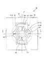
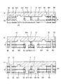
図1は、本発明の画像表示装置の第1実施形態を示す概略構成図、図2は、図1に示す画像表示装置が備える光スキャナーの上面図、図3は、図2中のA−A線断面図、図4は、図2に示す光スキャナーが有する電圧印加手段のブロック図、図5は、図4に示す第1の電圧発生部および第2の電圧発生部での発生電圧の一例を示す図である。なお、以下では、説明の便宜上、図3中の上側を「上」、下側を「下」と言う。
Hereinafter, preferred embodiments of a method for manufacturing an optical scanner, an image display device, a head mounted display, and an optical scanner will be described with reference to the accompanying drawings.
1. Image Display Device <First Embodiment>
FIG. 1 is a schematic configuration diagram showing a first embodiment of an image display device of the present invention, FIG. 2 is a top view of an optical scanner provided in the image display device shown in FIG. 1, and FIG. FIG. 4 is a block diagram of voltage application means included in the optical scanner shown in FIG. 2, and FIG. 5 is a diagram of the voltage generated by the first voltage generator and the second voltage generator shown in FIG. It is a figure which shows an example. In the following, for convenience of explanation, the upper side in FIG. 3 is referred to as “upper” and the lower side is referred to as “lower”.
図1に示す画像表示装置1は、スクリーン、壁面などの対象物10に描画用レーザー光LLを2次元的に走査することにより画像を表示する装置である。
図1および図4に示すように、画像表示装置1は、描画用レーザー光LLを出射する描画用光源ユニット2と、描画用レーザー光LLを走査する光スキャナー(本発明の光スキャナー)4と、光スキャナー4で走査した描画用レーザー光LLを反射させるミラー11と、描画用光源ユニット2および光スキャナー4の作動を制御する制御部6とを有している。なお、ミラー11は、必要に応じて設ければよく、省略してもよい。
An
As shown in FIGS. 1 and 4, the
≪描画用光源ユニット≫
図1に示すように、描画用光源ユニット2は、赤色、緑色、青色、各色のレーザー光源(光源部)21R、21G、21Bと、レーザー光源21R、21G、21Bに対応して設けられたコリメーターレンズ22R、22G、22Bおよびダイクロイックミラー23R、23G、23Bと、を備えている。
≪Light source unit for drawing≫
As shown in FIG. 1, the drawing light source unit 2 includes red, green, blue, and laser light sources (light source units) 21R, 21G, and 21B for each color and collimators provided corresponding to the
レーザー光源21R、21G、21Bは、それぞれ、図示しない光源と駆動回路とを有している。そして、レーザー光源21Rは、赤色のレーザー光RRを射出し、レーザー光源21Gは、緑色のレーザー光GGを出射し、レーザー光源21Bは、青色のレーザー光BBを出射する。レーザー光RR、GG、BBは、それぞれ、制御部6から送信される駆動信号に対応して出射され、コリメーターレンズ22R、22G、22Bによって平行光または略平行光にされる。レーザー光源21R、21G、21Bとしては、例えば、端面発光半導体レーザー、面発光半導体レーザーなどの半導体レーザーを用いることができる。半導体レーザーを用いることにより、レーザー光源21R、21G、21Bの小型化を図ることができる。
Each of the
このようなレーザー光源21R、21G、21Bの配置に倣って、ダイクロイックミラー23R、ダイクロイックミラー23B、ダイクロイックミラー23Gが配置されている。ダイクロイックミラー23Rは、レーザー光RRを反射する特性を有している。ダイクロイックミラー23Bは、レーザー光BBを反射するとともに、レーザー光RRを透過する特性を有している。ダイクロイックミラー23Gは、レーザー光GGを反射するとともに、レーザー光RR、BBを透過する特性を有している。これらダイクロイックミラー23R、23G、23Bによって、各色のレーザー光RR、GG、BBが合成されて描画用レーザー光LLとなる。
A
≪光スキャナー≫
光スキャナー4は、描画用光源ユニット2から描画用レーザー光LLを2次元走査する機能を有している。図2および図3に示すように、光スキャナー4は、構造体40と、永久磁石46と、コイル47と、磁心48と、電圧印加部49と、を備えている。また、構造体40は、可動部41と、1対の第1の軸部421、422と、枠体部43と、1対の第2の軸部441、442と、支持部45と、を有している。
≪Optical scanner≫
The
これらのうち可動部41、第1の軸部421、422は、第1の軸部421、422を軸として第1の軸J1周りに揺動(往復回動)する第1の振動系を構成する。また、可動部41、第1の軸部421、422、枠体部43、第2の軸部441、442および永久磁石46は、第2の軸J2周りに揺動(往復回動)する第2の振動系を構成する。また、永久磁石46、コイル47、磁心48および電圧印加部49は、前述した第1の振動系および第2の振動系を駆動させる駆動手段を構成する。
Among these, the
可動部41は、基部411と、基部411に設けられた光透過部412と、光透過部412に設けられた第1光反射低減部413とを有している。このような可動部41には描画用レーザー光LLが入射し、入射した描画用レーザー光LLの一部は、第1光反射低減部413の表面(光反射面413a)で反射され、その他は、光透過部412および基部411を透過(通過)したり、光透過部412で吸収されたりする。
The
基部411は、環状をなしており、中央部に貫通孔411aが形成されている。基部411は、光透過部412を支持する機能を有している。貫通孔411aは、光透過部412を透過した描画用レーザー光LLが通過する孔である。貫通孔411aは、基部411の機械的強度を維持できる限り大きいのが好ましい。言い換えれば、基部411の機械的強度を維持できる限り、基部411を薄肉化するのが好ましい。このような貫通孔411aを有することにより、光透過部412を透過した描画用レーザー光LLが基部411に照射されることに起因する基部411の発熱を抑制することができる。基部411の発熱を抑えることによって、光スキャナー4の熱歪みを抑制でき、光スキャナー4の光走査特性を維持することができる。
The
なお、基部411の構成としては、本実施形態のものに限定されず、例えば、基部411の一部が欠損していてもよい。すなわち、貫通孔411aが基部411の側面の一部に開放していてもよい。これにより、基部411の上面の面積をさらに小さくすることができるため、基部411の上面での描画用レーザー光LLの反射をより効果的に抑制することができる。
In addition, as a structure of the
このような基部411の上面側(描画用レーザー光LLが入射する側)には、貫通孔411aの上部開口を覆うように光透過部(第1光学部)412が設けられている。光透過部412をこのような配置とすることにより、光スキャナー4の構成が簡単なものとなる。光透過部412は、板状をなしており、その上面が平坦面で構成されている。光透過部412は、描画用レーザー光LLに対して高い光透過性を有している。
On the upper surface side (the side on which the drawing laser beam LL is incident) of such a
また、光透過部412の上面には、光反射を低減する第1光反射低減部(第2光学部)413が設けられており、下面には、光反射を低減する第3光反射低減部414が設けられている。これにより、描画用光源ユニット2から出射された描画用レーザー光LLの僅かしか光反射面413aで反射されないため、対象物10に表示される画像の輝度が抑えられる。そして、輝度が抑えられた分、コントラストが高められた画像を表示することができる。
In addition, a first light reflection reducing unit (second optical unit) 413 that reduces light reflection is provided on the upper surface of the
特に、第3光反射低減部414を設けることによって、より優れた画像表示特性が得られる。具体的には、光透過部412の下面は、光反射面413aと近接しかつ平行であることから、光透過部412の下面で反射された描画用レーザー光LLと、光反射面413aで反射された描画用レーザー光LLは、光軸が僅かにずれ、かつ、平行である。そのため、光透過部412の下面で描画用レーザー光LLが反射されてしまうと、光反射面413aで反射された描画用レーザー光LLによって描画される本来の画像と、光透過部412の下面で反射された描画用レーザー光LLによって描画される画像とがずれ重なって表示されてしまい(いわゆるゴーストが発生してしまい)、輪郭がぼやける等の画像品質の低下を引き起こすおそれがある。そのため、光透過部412の下面に第3光反射低減部414を設けてゴーストの発生を抑制することによって、より優れた画像表示特性が得られる。
In particular, by providing the third light
光透過部412、第1光反射低減部413および第3光反射低減部414により構成される光学部415の光透過率(描画用レーザー光LLの透過率)は、高いほど好ましい。具体的には、92%以上であるのが好ましく、99%以上であるのがより好ましい。これにより、描画用レーザー光LLが光学部415を透過する際、光学部415に吸収される描画用レーザー光LLの量を抑えることができ、光学部415の発熱(昇温)を抑制することができる。光学部415の発熱を抑えることにより、光スキャナー4の熱歪みを抑制でき、光スキャナー4の光走査特性を維持することができる。また、第1光反射低減部413の光透過率は、光透過部412の光透過率よりも高く設定されている。これにより、描画用光源ユニット2から出射された描画用レーザー光LLの僅かしか光反射面413aで反射されないため、対象物10に表示される画像の輝度が抑えられる。そして、輝度が抑えられた分、コントラストが高められた画像を表示することができる。
The higher the light transmittance (transmittance of the drawing laser beam LL) of the
また、光学部415の光反射率(描画用レーザー光LLの反射率)は、0%でない限りは、低いほど好ましい。具体的には、4%未満であるのが好ましく、1%未満であるのがより好ましい。これにより、描画用光源ユニット2から出射された描画用レーザー光LLの僅かしか光反射面413aで反射されないため、対象物10に表示される画像の輝度が抑えられる。そして、輝度が抑えられた分、コントラストが高められた画像を表示することができる。
Further, the light reflectance of the optical unit 415 (the reflectance of the drawing laser beam LL) is preferably as low as possible unless it is 0%. Specifically, it is preferably less than 4%, and more preferably less than 1%. Thereby, since only a part of the drawing laser beam LL emitted from the drawing light source unit 2 is reflected by the
ここで、光学部415の光透過率および光反射率は、光透過部412、第1、第3光反射低減部413、414の材料によっては波長依存性を有している場合がある。この場合、レーザー光RR、GG、BB全ての光において光反射率が92%以上であり、光透過率が4%未満であることが好ましいが、レーザー光RR、GG、BBの少なくとも1つの光において、光反射率が92%以上であり、光透過率が4%未満であってもよい。
Here, the light transmittance and light reflectance of the
光透過部412の構成材料としては、描画用レーザー光LLに対して高い光透過性を有していれば、特に限定されないが、実質的に無色透明な材料を用いるのが好ましい。無色透明な材料としては、例えば、石英ガラス、パイレックスガラス(「パイレックス」は登録商標)、テンパックスガラス等のガラス材料や、水晶等が挙げられる。さらに、これらの中でも、基部411の構成材料の熱膨張係数とより近い熱膨張係数を有する材料を用いるのが好ましい。
The constituent material of the
光透過部412の厚さとしては、特に限定されないが、光透過部412に必要な機械的強度を維持できる限りより薄いのが好ましい。具体的には、30μm以上、200μm以下程度であるのが好ましい。これにより、描画用レーザー光LLが光透過部412を通過する際、光透過部412に吸収される描画用レーザー光LLの量を抑えることができ、光透過部412の発熱を抑制することができる。光透過部412の発熱を抑えることによって、光スキャナー4の熱歪みを抑制でき、光スキャナー4の光走査特性を維持することができる。
The thickness of the
第1、第3光反射低減部413、414としては、反射を低減することができれば、特に限定されないが、例えば、公知の各種反射防止膜(ARコート)を用いることができる。すなわち、第1光反射低減部413は、例えば、高屈折率層と低屈折率層とが交互に複数積層されてなる誘電体多層膜で構成することができる。前記高屈折率層を構成する材料としては、第1光反射低減部413に必要な光学特性を得ることができるものであれば、特に限定されず、Ti2O、Ta2O5、酸化ニオブなどが挙げられる。一方、低屈折率層を構成する材料としては、第1光反射低減部413に必要な光学特性を得ることができるものであれば、特に限定されず、例えば、MgF2、SiO2などが挙げられる。
The first and third light
以上、可動部41について説明した。本実施形態では、基部411および光透過部412は、平面視にて、それぞれ円形をなしているが、基部411および光透過部412の平面視形状は、これに限定されず、例えば、楕円形、三角形、四角形等の多角形であってもよい。
枠体部43は、枠状をなし、可動部41の基部411を囲んで設けられている。言い換えると、可動部41の基部411は、枠状をなす枠体部43の内側に設けられている。可動部41の基部411は、1対の第1の軸部421、422を介して枠体部43に支持されている。また、枠体部43は、1対の第2の軸部441、442を介して支持部45に支持されている。
The
The
また、枠体部43は、第1の軸J1に沿った方向での長さが第2の軸J2に沿った方向での長さよりも長くなっている。すなわち、第1の軸J1に沿った方向における枠体部43の長さをaとし、第2の軸J2に沿った方向における枠体部43の長さをbとしたとき、a>bなる関係を満たす。これにより、第1の軸部421、422に必要な長さを確保しつつ、第2の軸J2に沿った方向における光スキャナー4の長さを抑えることができる。
Further, the length of the
また、枠体部43は、平面視にて、基部411および1対の第1の軸部421、422からなる構造体の外形に沿った形状をなしている。これにより、可動部41、1対の第1の軸部421、422で構成された第1の振動系の振動、すなわち、可動部41の第1の軸J1周りの揺動を許容しつつ、枠体部43の小型化を図ることができる。なお、枠体部43の形状は、枠状であれば、図示のものに限定されない。
Further, the
第1の軸部421、422および第2の軸部441、442は、それぞれ、弾性変形可能である。そして、第1の軸部421、422は、可動部41を第1の軸J1周りに揺動可能とするように、可動部41と枠体部43を連結している。また、第2の軸部441、442は、枠体部43を第1の軸J1に直交する第2の軸J2周りに揺動可能とするように、枠体部43と支持部45を連結している。
The
第1の軸部421、422は、可動部41の基部411を介して互いに対向するように配置されている。また、第1の軸部421、422は、それぞれ、第1の軸J1に沿った方向に延在する長手形状をなす。そして、第1の軸部421、422は、それぞれ、一端部が基部411に接続され、他端部が枠体部43に接続されている。また、第1の軸部421、422は、それぞれ、中心軸が第1の軸J1に一致するように配置されている。このような第1の軸部421、422は、それぞれ、可動部41の第1の軸J1周りの揺動に伴ってねじれ変形する。
The
第2の軸部441、442は、枠体部43を介して互いに対向するように配置されている。また、第2の軸部441、442は、それぞれ、第2の軸J2に沿った方向に延在する長手形状をなす。そして、第2の軸部441、442は、それぞれ、一端部が枠体部43に接続され、他端部が支持部45に接続されている。また、第2の軸部441、442は、それぞれ、中心軸が第2の軸J2に一致するように配置されている。このような第2の軸部441、442は、枠体部43の第2の軸J2周りの揺動に伴ってねじれ変形する。
The
このように、可動部41を第1の軸J1周りに揺動可能とするとともに、枠体部43を第2の軸J2周りに揺動可能とすることにより、可動部41(光反射面413a)を互いに直交する第1、第2の軸J1、J2の2軸周りに揺動させることができる。
なお、第1の軸部421、422および第2の軸部441、442の形状は、それぞれ、前述したものに限定されず、例えば、途中の少なくとも1箇所に屈曲または湾曲した部分や分岐した部分を有していてもよい。また、各軸部421、422、441、442を2本の軸部に分割してもよい。
As described above, the
Note that the shapes of the
以上、構造体40について説明した。本実施形態では、平面視にて、構造体40の光反射面413aの下側および外側に位置する領域、言い換えれば、第1光反射低減部413、光透過部412を透過し貫通孔411aを通過した描画用レーザー光LLおよび光反射面413aの周囲に照射された描画用レーザー光LLが照射され得る領域に反射防止膜(反射低減部)5が設けられている。具体的には、基部411、第1の軸部421、422、枠体部43、第2の軸部441、442、支持部45の各上面、さらには、光透過部412の下面に、反射防止膜5が設けられている。反射防止膜5は、構造体40の光反射面413aの下側および外側に位置する領域に入射する描画用レーザー光LLの反射率を低減する(好ましくは零とする)機能を有している。これにより、不要な描画用レーザー光LLが迷光となるのを防止することができるため、優れた光走査特性が得られる。なお、反射防止膜5は、さらに、基部411の内外周面、枠体部43の内外周面および支持部45の内周面に設けてもよく、この場合は上記効果がより向上する。
The
なお、反射防止膜5に換えて、粗面化処理、黒色処理等を行ってもよい。これによっても、反射防止膜5と同様の効果を得ることができる。
また、構造体40とコイル47との間(光透過部412の第1光反射低減部413が設けられた表面と反対側)には、ベース71に支持された第2光反射低減部7が設けられている。第2光反射低減部7は、光学部415を透過した描画用レーザー光LLの反射率を低減する(好ましくは零とする)機能を有している。第2光反射低減部7は、可動部41(光透過部412)、基部411と枠体部43の隙間および枠体部43と支持部45の隙間の各々と対向するように配置されているため、光学部415を透過した不要な描画用レーザー光LLや前記隙間を通過した不要な描画用レーザー光LLが迷光となるのを防止することができ、優れた光走査特性が得られる。第2光反射低減部7は、前述した第1光反射低減部413と同様の構成(反射防止膜)とすることができる。なお、第2光反射低減部7は、反射率を低減できれば、ベース71の表面に粗面化処理、黒色処理等を行った構成であってもよい。
Instead of the
Further, between the
基部411、第1の軸部421、422、枠体部43、第2の軸部441、442および支持部45は、一体的に形成されている。本実施形態では、基部411、第1の軸部421、422、枠体部43、第2の軸部441、442および支持部45は、第1のSi層(デバイス層)と、SiO2層(ボックス層)と、第2のSi層(ハンドル層)とがこの順に積層したSOI基板をエッチングすることにより形成されている。これにより、第1の振動系および第2の振動系の振動特性を優れたものとすることができる。また、SOI基板は、エッチングにより微細な加工が可能であるため、SOI基板を用いて基部411、第1の軸部421、422、枠体部43、第2の軸部441、442および支持部45を形成することにより、これらの寸法精度を優れたものとすることができ、また、光スキャナー4の小型化を図ることができる。
The
基部411、第1の軸部421、422および第2の軸部441、442は、それぞれ、SOI基板の第1のSi層で構成されている。これにより、第1の軸部421、422および第2の軸部441、442の弾性を優れたものとすることができる。また、基部411が第1の軸J1周りに回動する際に枠体部43に接触するのを防止することができる。また、枠体部43および支持部45は、それぞれ、SOI基板の第1のSi層、SiO2層および第2のSi層からなる積層体で構成されている。これにより、枠体部43および支持部45の剛性を優れたものとすることができる。また、枠体部43のSiO2層および第2のSi層は、枠体部43の剛性を高めるリブとしての機能だけでなく、可動部41が永久磁石46に接触するのを防止する機能も有する。
前述した枠体部43の下面には、永久磁石46が接合されている。永久磁石46と枠体部43との接合方法としては、特に限定されないが、例えば、接着剤を用いた接合方法を用いることができる。永久磁石46は、平面視にて、第1、第2の軸J1、J2に対して傾斜する方向に磁化されている。
The
A
本実施形態では、永久磁石46は、第1、第2の軸J1、J2の両軸に対して傾斜する方向に延在する長手形状(棒状)をなす。そして、永久磁石46は、その長手方向に磁化されている。すなわち、永久磁石46は、一端部をS極とし、他端部をN極とするように磁化されている。また、永久磁石46は、平面視にて、第1の軸J1と第2の軸J2との交点を中心として対称となるように設けられている。
In the present embodiment, the
第2の軸J2に対する永久磁石46の磁化の方向(延在方向)の傾斜角θは、特に限定されないが、30°以上60°以下であるのが好ましく、45°以上60°以下であることがより好ましく、45°であるのがさらに好ましい。このように永久磁石46を設けることにより、円滑かつ確実に、可動部41(光反射面413a)を第2の軸J2周りに揺動させることができる。
The inclination angle θ in the magnetization direction (extending direction) of the
このような永久磁石46としては、例えば、ネオジム磁石、フェライト磁石、サマリウムコバルト磁石、アルニコ磁石、ボンド磁石等を好適に用いることができる。このような永久磁石46は、硬磁性体を着磁したものであり、例えば、着磁前の硬磁性体を枠体部43に設置した後に着磁することにより形成される。既に着磁がなされた永久磁石46を枠体部43に設置しようとすると、外部や他の部品の磁界の影響により、永久磁石46を所望の位置に設置できない場合があるからである。
As such a
永久磁石46の直下には、コイル47が設けられている。これにより、コイル47から発生する磁界を効率的に永久磁石46に作用させることができる。これにより、光スキャナー4の省電力化および小型化を図ることができる。コイル47は、磁心48に巻回されて設けられている。これにより、コイル47で発生した磁界を効率的に永久磁石46に作用させることができる。なお、磁心48は、省略してもよい。
A
このようなコイル47は、電圧印加部49に電気的に接続されている。そして、電圧印加部49によりコイル47に電圧が印加されることで、コイル47から第1、第2の軸J1、J2に直交する磁束を有する磁界が発生する。
電圧印加部49は、図4に示すように、可動部41を第1の軸J1周りに回動させるための第1の電圧V1を発生させる第1の電圧発生部491と、可動部41を第2の軸J2周りに回動させるための第2の電圧V2を発生させる第2の電圧発生部492と、第1の電圧V1と第2の電圧V2とを重畳する電圧重畳部493とを備え、電圧重畳部493で重畳した電圧をコイル47に印加する。
Such a
As shown in FIG. 4, the
第1の電圧発生部491は、図5(a)に示すように、周期T1で周期的に変化する第1の電圧V1(主走査用電圧)を発生させるものである。第1の電圧V1は、正弦波のような波形をなしている。第1の電圧V1の周波数(1/T1)は、例えば、10〜40kHzであるのが好ましい。本実施形態では、第1の電圧V1の周波数は、可動部41、1対の軸部421、422で構成される第1の振動系のねじり共振周波数(f1)と等しくなるように設定されている。これにより、可動部41の第1の軸J1周りの回動角を大きくすることができる。
As shown in FIG. 5A, the first voltage generator 491 generates a first voltage V1 (main scanning voltage) that periodically changes in a cycle T1. The first voltage V1 has a waveform like a sine wave. The frequency (1 / T1) of the first voltage V1 is preferably 10 to 40 kHz, for example. In the present embodiment, the frequency of the first voltage V1 is set to be equal to the torsional resonance frequency (f1) of the first vibration system including the
一方、第2の電圧発生部492は、図5(b)に示すように、周期T1と異なる周期T2で周期的に変化する第2の電圧V2(副走査用電圧)を発生させるものである。第2の電圧V2は、鋸波のような波形をなしている。第2の電圧V2の周波数(1/T2)は、第1の電圧V1の周波数(1/T1)と異なっていればよく、例えば、30〜120Hz(60Hz程度)であるのが好ましい。本実施形態では、第2の電圧V2の周波数は、可動部41、1対の第1の軸部421、422、枠体部43、1対の第2の軸部441、442および永久磁石46で構成された第2の振動系のねじり共振周波数(共振周波数)と異なる周波数となるように調整されている。
このような第2の電圧V2の周波数は、第1の電圧V1の周波数よりも小さいことが好ましい。これにより、より確実かつより円滑に、可動部41を第1の軸J1周りに第1の電圧V1の周波数で揺動させつつ、第2の軸J2周りに第2の電圧V2の周波数で揺動させることができる。
On the other hand, as shown in FIG. 5B, the
The frequency of the second voltage V2 is preferably smaller than the frequency of the first voltage V1. As a result, the
また、第1の振動系のねじり共振周波数をf1[Hz]とし、第2の振動系のねじり共振周波数をf2[Hz]としたとき、f1とf2とが、f2<f1の関係を満たすことが好ましく、10f2≦f1の関係を満たすことがより好ましい。これにより、より円滑に、可動部41を、第1の軸J1周りに第1の電圧V1の周波数で回動させつつ、第2の軸J2周りに第2の電圧V2の周波数で回動させることができる。これに対し、f1≦f2とした場合は、第2の電圧V2の周波数による第1の振動系の振動が発生する可能性がある。
Further, when the torsional resonance frequency of the first vibration system is f1 [Hz] and the torsional resonance frequency of the second vibration system is f2 [Hz], f1 and f2 satisfy the relationship of f2 <f1. Is preferable, and it is more preferable to satisfy the relationship of 10f2 ≦ f1. As a result, the
このような第1の電圧発生部491および第2の電圧発生部492は、それぞれ、制御部6に接続され、この制御部6からの信号に基づき駆動する。このような第1の電圧発生部491および第2の電圧発生部492には、電圧重畳部493が接続されている。
電圧重畳部493は、コイル47に電圧を印加するための加算器493aを備えている。加算器493aは、第1の電圧発生部491から第1の電圧V1を受けるとともに、第2の電圧発生部492から第2の電圧V2を受け、これらの電圧を重畳しコイル47に印加するようになっている。
The first voltage generation unit 491 and the second
The
次に、光スキャナー4の駆動方法について説明する。なお、第1の電圧V1の周波数は、第1の振動系のねじり共振周波数と等しく設定されており、第2の電圧V2の周波数は、第2の振動系のねじり共振周波数と異なる値に、かつ、第1の電圧V1の周波数よりも小さくなるように設定されている(例えば、第1の電圧V1の周波数が18kHz、第2の電圧V2の周波数が60Hzに設定されている)ものとする。
Next, a method for driving the
例えば、図5(a)に示す第1の電圧V1と、図5(b)に示す第2の電圧V2とを電圧重畳部493にて重畳し、重畳した電圧をコイル47に印加する。すると、第1の電圧V1によって、永久磁石46の一端部(N極)をコイル47に引き付けようとするとともに、永久磁石46の他端部(S極)をコイル47から離間させようとする磁界(この磁界を「磁界A1」という)と、永久磁石46の一端部(N極)をコイル47から離間させようとするとともに、永久磁石46の他端部(S極)をコイル47に引き付けようとする磁界(この磁界を「磁界A2」という)とが交互に切り換わる。
For example, the
このように磁界A1と磁界A2とが交互に切り換わることで、枠体部43に第1の軸J1周りのねじり振動成分を有する振動が励振され、その振動に伴って、第1の軸部421、422を捩れ変形させつつ、可動部41が第1の電圧V1の周波数で第1の軸J1周りに揺動する。なお、第1の電圧V1の周波数は、第1の振動系のねじり共振周波数と等しいため、共振振動によって、可動部41を大きく揺動させることができる。
As the magnetic field A1 and the magnetic field A2 are alternately switched in this way, vibration having a torsional vibration component around the first axis J1 is excited in the
一方、第2の電圧V2によって、永久磁石46の一端部(N極)をコイル47に引き付けようとするとともに、永久磁石46の他端部(S極)をコイル47から離間させようとする磁界(この磁界を「磁界B1」という)と、永久磁石46の一端部(N極)をコイル47から離間させようとするとともに、永久磁石46の他端部(S極)をコイル47に引き付けようとする磁界(この磁界を「磁界B2」という)とが交互に切り換わる。
On the other hand, the second voltage V <b> 2 is used to attract one end (N pole) of the
このように磁界B1と磁界B2とが交互に切り換わることで、第2の軸部441、442を捩れ変形させつつ、枠体部43が可動部41とともに、第2の電圧V2の周波数で第2の軸J2周りに揺動する。なお、前述のように、第2の電圧V2の周波数が第1の電圧V1の周波数に比べて極めて低く設定され、第2の振動系のねじり共振周波数が第1の振動系のねじり共振周波数よりも低く設計されているため、可動部41が第2の電圧V2の周波数で第1の軸J1周りに回動してしまうことを防止することができる。
As the magnetic field B1 and the magnetic field B2 are alternately switched in this way, the
このように、光スキャナー4では、第1の電圧V1と第2の電圧V2とを重畳させた電圧をコイル47に印加することで、可動部41を、第1の軸J1周りに第1の電圧V1の周波数で回動させつつ、第2の軸J2周りに第2の電圧のV2の周波数で回動させることができる。これにより、装置の低コスト化および小型化を図ることができる。また、電磁駆動方式(ムービングマグネット方式)を採用することによって、確実に、可動部41を第1、第2の軸J1、J2のそれぞれの軸周りに揺動させ、第1光反射低減部413で反射した描画用レーザー光LLを2次元走査することができる。また、駆動源を構成する部品(永久磁石およびコイル)の数を少なくすることができるため、簡単かつ小型な構成とすることができる。また、コイル47が光スキャナー4の振動系と離間しているので、かかる振動系に対するコイル47の発熱による悪影響を防止することができる。
As described above, in the
以上、光スキャナー4について詳細に説明した。本実施形態のようなジンバル型をなす2次元走査型の光スキャナー4によれば、1つの装置で描画用レーザー光LLを2次元走査することができるため、例えば、1次元走査型の光スキャナーを2つ組み合わせて描画用レーザー光LLを2次元走査させる構成と比較して、装置の小型化を図ることができるとともに、アライメントの調整も容易となる。
The
≪制御部≫
制御部6は、描画用光源ユニット2および光スキャナー4の作動を制御する機能を有している。具体的には、制御部6は、光スキャナー4を駆動して可動部41を第1、第2の軸J1、J2周りに揺動させるとともに、可動部41の揺動に同期させて描画用光源ユニット2から描画用レーザー光LLを出射させる。制御部6は、例えば外部コンピューターから送信された画像データに基づいて、各レーザー光源21R、21G、21Bから所定強度のレーザー光RR、GG、BBを所定のタイミングで出射させ、所定色および強度(輝度)の描画用レーザー光LLを所定タイミングで出射させる。これにより、対象物10に画像データに応じた画像が表示される。
≪Control part≫
The control unit 6 has a function of controlling the operations of the drawing light source unit 2 and the
以上、画像表示装置1の構成について詳細に説明した。このような画像表示装置1によれば、描画用レーザー光LLの一部を光スキャナー4によって対象物10に走査するため、描画用レーザー光LLの輝度(強度)を抑えることができる。そのため、対象物10に表示される画像のコントラストを高めることができる。このように、画像表示装置1では、対象物10に走査される描画用レーザー光LLの輝度(強度)を抑えるために、各レーザー光源21R、21G、21Bの出力を抑える必要がないため、各レーザー光源21R、21G、21Bから安定してレーザー光RR、GG、BBを出射させることができ、優れた画像表示特性を発揮することができる。
The configuration of the
また、光スキャナー4の光反射面413aで反射されなかった描画用レーザー光LLは、光透過部412を通過するが、光透過部412が高い光透過性を有しているため、光透過部412での描画用レーザー光LLの吸収が抑制(防止)される。そのため、可動部41の発熱が抑制され、熱応力による光スキャナー4の振動特性の低下(変化)を効果的に抑制することができる。また、光スキャナー4に反射防止膜5および第2光反射低減部7を設けているため、光スキャナー4の光反射面413aで反射されなかった描画用レーザー光LLが迷光となるのを防止することができる。
Further, the drawing laser beam LL that has not been reflected by the
なお、従来のように、各レーザー光源21R、21G、21Bの出力を抑えることにより描画用レーザー光LLの輝度を抑えようとしても、描画用レーザー光LLの輝度を十分に落とすことができないし、各レーザー光源21R、21G、21Bの駆動が不安定となり、安定したレーザー光RR、GG、BBの出射を行うことができないという問題がある。
Note that, as in the prior art, even if it is attempted to suppress the luminance of the drawing laser beam LL by suppressing the output of each of the
<第2実施形態>
次に、本発明の画像表示装置の第2実施形態について説明する。
図6は、本発明の第2実施形態にかかる画像表示装置が備える光スキャナーの上面図、図7は、図6中のB−B線断面図である。
以下、第2実施形態の画像表示装置について、前述した実施形態との相違点を中心に説明し、同様の事項については、その説明を省略する。
本発明の第2実施形態にかかる画像表示装置は、光スキャナーの可動部の構成が異なること以外は、前述した第1実施形態と同様である。なお、前述した第1実施形態と同様の構成には、同一符号を付してある。
Second Embodiment
Next, a second embodiment of the image display device of the present invention will be described.
FIG. 6 is a top view of an optical scanner provided in the image display apparatus according to the second embodiment of the present invention, and FIG. 7 is a cross-sectional view taken along line BB in FIG.
Hereinafter, the image display apparatus according to the second embodiment will be described focusing on the differences from the above-described embodiment, and description of similar matters will be omitted.
The image display apparatus according to the second embodiment of the present invention is the same as that of the first embodiment described above except that the configuration of the movable portion of the optical scanner is different. In addition, the same code | symbol is attached | subjected to the structure similar to 1st Embodiment mentioned above.
≪光スキャナー≫
図6および図7に示すように、本実施形態の光スキャナー4Aの可動部41Aは、基部411Aと、基部411Aに嵌め込まれた光透過部412と、光透過部412に設けられた第1、第3光反射低減部413、414とを有している。
基部411Aは、環状をなし、その中央部に貫通孔411aを有している。貫通孔411aの軸方向の途中には段差が形成されている。具体的には、貫通孔411aは、第1の貫通孔411a’と、第1の貫通孔411a’の下側に連結する第2の貫通孔411a”とを有しており、第2の貫通孔411a”は、第1の貫通孔411a’と同軸的に設けられ、かつ、第1の貫通孔411a’よりも径が小さい。そして、第1の貫通孔411a’と第2の貫通孔411a”の接続部に前記段差が形成されている。
≪Optical scanner≫
As shown in FIGS. 6 and 7, the
The base 411 A is an annular, has a through
このような基部411Aの第1の貫通孔411a’には、光透過部412が嵌め込まれており、光透過部412の下面は前記段差部に当接している。このように、貫通孔411a内に光透過部412を設けることにより、例えば第1実施形態の光スキャナー4と比較して高さを抑えることができ、光スキャナー4Aの小型化(低背化)を図ることができる。また、前記段差が、光透過部412を第1の貫通孔411a’に嵌め込む際のストッパー(位置決め手段)として機能するため、光透過部412の配置を正確に制御することができる。
The
また、基部411Aは、枠体部43や支持部45と同様にSOI基板の第1のSi層、SiO2層および第2のSi層からなる積層体で構成されている。これにより、基部411Aの剛性を優れたものとすることができる。また、例えば、第1のSi層で第1の貫通孔411a’を形成し、SiO2層および第2のSi層で第2の貫通孔411a”を形成することによって、簡単に段差を有する貫通孔411aを形成することができる。
このような第2実施形態によっても、前述した第1実施形態と同様の効果を奏することができる。
In addition, the
Also according to the second embodiment, the same effects as those of the first embodiment described above can be obtained.
<第3実施形態>
次に、本発明の画像表示装置の第3実施形態について説明する。
図8は、本発明の第3実施形態にかかる画像表示装置が備える光スキャナーの上面図、図9は、図8中のC−C線断面図である。
以下、第3実施形態の画像表示装置について、前述した実施形態との相違点を中心に説明し、同様の事項については、その説明を省略する。
本発明の第3実施形態にかかる画像表示装置は、光スキャナーの可動部の構成が異なること以外は、前述した第1実施形態と同様である。なお、前述した第1実施形態と同様の構成には、同一符号を付してある。
<Third Embodiment>
Next, a third embodiment of the image display device of the present invention will be described.
FIG. 8 is a top view of the optical scanner provided in the image display apparatus according to the third embodiment of the present invention, and FIG. 9 is a cross-sectional view taken along the line CC in FIG.
Hereinafter, the image display apparatus according to the third embodiment will be described focusing on the differences from the above-described embodiment, and description of similar matters will be omitted.
The image display apparatus according to the third embodiment of the present invention is the same as that of the first embodiment described above except that the configuration of the movable portion of the optical scanner is different. In addition, the same code | symbol is attached | subjected to the structure similar to 1st Embodiment mentioned above.
≪光スキャナー≫
図8および図9に示すように、本実施形態の光スキャナー4Bの可動部41Bは、基部411Bと、スペーサー416Bを介して基部411Bに固定された板状の光透過部412Bと、光透過部412Bの上面に形成された第1光反射低減部413と、光透過部412Bの下面に形成された第3光反射低減部414とを有している。
≪Optical scanner≫
As shown in FIGS. 8 and 9, the
第1光反射低減部413は、第1の軸部421、422に対して光透過部412Bの板厚方向に離間するとともに、平面視にて、第1の軸部421、422と重なって設けられている。そのため、第1の軸部421、422の間の距離を短くしつつ、光透過部412Bの板面の面積(第1光反射低減部413の面積)を大きくすることができる。また、第1の軸部421、422の間の距離を短くすることできることから、枠体部43の小型化を図ることができる。さらに、枠体部43の小型化を図ることができることから、第2の軸部441、442の間の距離を短くすることできる。このようなことから、光透過部412Bの板面の面積(第1光反射低減部413の面積)を大きくしても、光スキャナー4の小型化を図ることができる。
The first light
このような光スキャナー4Bでは、平面視にて、光反射面413aの下側および外側に位置する領域、具体的には、基部411B、第1の軸部421、422、枠体部43、第2の軸部441、442、支持部45の上面に反射防止膜5が設けられている。これにより、第1光反射低減部413以外に照射された描画用レーザー光LLが迷光となるのを防止することができる。なお、反射防止膜5は、例えば、スペーサー414B、基部411B、枠体部43および支持部45の側面にも設けてもよい。これにより、上記効果がより向上する。
このような第3実施形態によっても、前述した第1実施形態と同様の効果を奏することができる。
In such an
According to the third embodiment, the same effect as that of the first embodiment described above can be obtained.
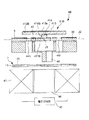
2.光スキャナーの製造方法
次に、図10ないし図13に基づいて、光スキャナーの製造方法について説明する。なお、以下に記載の光スキャナーの製造方法では前述の第3実施形態に似た構成の光スキャナーが得られる。
光スキャナーの製造方法は、第2のSi層84(基部)およびスペーサー914(突出部)を有する積層基板(基板)8と、一方の面側に凸部31が形成されたガラス基板(透明基板)3とを用意し、積層基板8とガラス基板3をと重ね合わせて、スペーサー914と凸部31とを接合する接合工程と、第2のSi層84をパターニングし、スペーサー914を支持する基部911と、第1の軸部921、922と、枠体部93と、第2の軸部941、942と、支持部95とを形成するパターニング工程と、積層基板8とガラス基板3の隙間に封止材100を充填する充電工程と、凸部31を残して、ガラス基板3を薄肉化することによって、光透過部912を形成する薄肉化工程と、光透過部912の表面に、光反射を低減する第1光反射低減部413を形成する光反射低減部形成工程と、を有している。以下、この製造方法について詳細に説明する。
2. Optical Scanner Manufacturing Method Next, an optical scanner manufacturing method will be described with reference to FIGS. The optical scanner manufacturing method described below provides an optical scanner having a configuration similar to that of the third embodiment.
The manufacturing method of the optical scanner includes a laminated substrate (substrate) 8 having a second Si layer 84 (base portion) and a spacer 914 (protrusion portion), and a glass substrate (transparent substrate) having a
[1]接合工程
[1−1]積層基板加工工程
まず、図10(a)に示すように、上側から第1のSiO2層81、第1のSi層82、第2のSiO2層83、第2のSi層84および第3のSiO2層85が積層してなる積層基板8を用意する。各層の厚さとしては、特に限定されないが、例えば、第1のSiO2層81:1.6μm程度、第1のSi層82:250μm程度、第2のSiO2層83:0.5μm程度、第2のSi層84:40μm程度、第3のSiO2層85:0.5μm程度とすることができる。
[1] Joining Step [1-1] Laminate Substrate Processing Step First, as shown in FIG. 10A, the first SiO 2 layer 81, the
次に、図10(b)に示すように、例えばドライエッチング(2段階のドライエッチング)によって、スペーサー(支柱)914、枠体部93のリブ部931、支持部95のリブ部951および支持部95の外周を囲む枠部96の一部を形成する。具体的には、まずスペーサー(支柱)914、支持部95のリブ部951および枠部96に対応する位置に第1のSiO2層81をパターニングして形成したSiO2マスクを、枠体部93のリブ部931に対応する位置に、レジストマスクを設ける。次に、1段階目のドライエッチングを行い、レジストマスク除去後に2段階目のドライエッチングを実施する。次に、図10(c)に示すように、例えばウエットエッチングによって、第1のSiO2層81と第1のSi層82から露出する第2のSiO2層83を除去する。
次に、図10(d)に示すように、例えばドライエッチングによって、第3のSiO2層85をパターニングして、基部911、第1の軸部921、922、枠体部93、第2の軸部941、942、支持部95の平面視形状に対応した形状の第3のSiO2層85を得る。
Next, as shown in FIG. 10B, for example, by dry etching (two-stage dry etching), spacers (supports) 914,
Next, as shown in FIG. 10D, the third SiO 2 layer 85 is patterned by dry etching, for example, so that the
[1−2]ガラス基板加工工程
まず、図11(a)に示すように、実質的に無色透明なガラス基板(例えば、テンパックスガラス基板)3を準備する。ガラス基板3の厚さとしては、特に限定されないが、例えば、400μm程度とすることができる。次に、図11(b)に示すように、例えばウエットエッチングによって、ガラス基板3の上面をパターニングすることにより、光透過部912の平面視形状に対応する凸部31と、支持部95の平面視形状に対応する凸部32と、枠部96と接合するための凸部33とを形成する。凸部31〜33の高さとしては特に限定されないが、例えば、それぞれ、80μm程度とすることができる。
なお、この後、必要に応じて、凸部31の上面に反射防止膜を成膜してもよい。反射防止膜を成膜することによって、光透過部912の下面に反射防止膜が形成された光スキャナーが得られる。
[1-2] Glass Substrate Processing Step First, as shown in FIG. 11A, a substantially colorless and transparent glass substrate (for example, Tempax glass substrate) 3 is prepared. Although it does not specifically limit as thickness of the
After that, an antireflection film may be formed on the upper surface of the
[1−3]接合工程
まず、図12(a)に示すように、前記工程[1−1]で得られた積層基板8と、前記工程[1−2]で得られたガラス基板3とを、凸部31とスペーサー914、凸部32とリブ部951、凸部33と枠部96とを対向させて接合する。なお、接合方法としては、特に限定されないが、陽極接合を用いるのが好ましい。これにより、積層基板8とガラス基板3とを確実かつ強固に接合することができる。
[1-3] Joining Step First, as shown in FIG. 12A, the
[2]パターニング工程(シリコンエッチング工程)
次に、図12(b)に示すように、例えばドライエッチングによって、第2のSi層84をエッチングして、基部911、第1の軸部921、922、枠体部93、第2の軸部941、942、支持部95を得る。
[3]充填工程
次に、図12(c)に示すように、第2のSi層84に形成された隙間から、ワックス等の封止材100を供給し、ガラス基板3と積層基板8の間の隙間を封止材100で埋める。
[2] Patterning process (silicon etching process)
Next, as shown in FIG. 12B, the
[3] Filling Step Next, as shown in FIG. 12C, a sealing
[4]薄肉化工程
次に、図13(a)に示すように、積層基板8を下側にして、ガラス基板3と積層基板8の積層体を支持基板110に固定する。この固定には、封止材100が用いられる。次に、図13(b)に示すように、例えばウエットエッチングによってガラス基板3をエッチングして薄肉化する。これにより、凸部31〜33以外の部分が除去されて、凸部31〜33がそれぞれ独立し、光透過部912、枠体部93、支持部95が得られる。また、凸部31〜33の高さが調節される。ここで、積層基板8が封止材100で保護されているため、本工程にて、エッチング液が積層基板8に接触することがなく、積層基板8のダメージを防止することができる。
なお、ガラス基板3の加工方法としてはウエットエッチングに限定されず、例えば、研磨加工であってもよい。研磨加工の場合も封止材100で保護することで研磨時の構造体の破損を解消できる。
[4] Thinning Step Next, as shown in FIG. 13A, the laminated body of the
In addition, as a processing method of the
[5]光反射層形成工程
次に、アセトンなどの溶剤を用いて封止材100を除去し、その後、ダイシング等によって枠部96からその内側の部分を切り取る。そして、光透過部912の上面に、例えば反射防止膜を成膜することによって光反射層913を形成する。以上により、図13(c)に示すように、光スキャナー9(構造体90)が得られる。
このような光スキャナーの製造方法によれば、簡単かつ精度よく、光透過部を有する光スキャナーを製造することができる。
[5] Light Reflecting Layer Formation Step Next, the sealing
According to such a method for manufacturing an optical scanner, an optical scanner having a light transmission part can be manufactured easily and accurately.
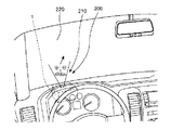
[ヘッドアップディスプレイ]
次に、本発明の画像表示装置の一例であるヘッドアップディスプレイについて説明する。
図14は、本発明の画像表示装置を応用したヘッドアップディスプレイを示す斜視図である。
図14に示すように、ヘッドアップディスプレイシステム200では、画像表示装置1は、自動車のダッシュボードに、ヘッドアップディスプレイ210を構成するよう搭載されている。このヘッドアップディスプレイ210により、フロントガラス220に、例えば、目的地までの案内表示等の所定の画像を表示することができる。なお、ヘッドアップディスプレイシステム200は、自動車に限らず、例えば、航空機、船舶等にも適用することができる。
[Head-up display]
Next, a head-up display which is an example of the image display device of the present invention will be described.
FIG. 14 is a perspective view showing a head-up display to which the image display device of the present invention is applied.
As shown in FIG. 14, in the head-up
[ヘッドマウントディスプレイ]
次に、本発明のヘッドマウントディスプレイについて説明する。
図15は、本発明のヘッドマウントディスプレイを示す斜視図である。
図15に示すように、ヘッドマウントディスプレイ300は、観察者の頭部に装着されるフレーム310と、フレーム310に搭載された画像表示装置1とを有している。そして、画像表示装置1により、フレーム310の本来レンズである部位に設けられた表示部(光反射層材)320に、一方の目で視認される所定の画像を表示する。
[Head mounted display]
Next, the head mounted display of the present invention will be described.
FIG. 15 is a perspective view showing the head mounted display of the present invention.
As shown in FIG. 15, the head-mounted
表示部320は、透明であってもよく、また、不透明であってもよい。表示部320が透明な場合は、現実世界からの情報に画像表示装置1からの情報を重ねて使用することができる。また、表示部320は、入射した光の少なくとも一部を反射すればよく、例えば、ハーフミラーなどを用いることができる。
なお、ヘッドマウントディスプレイ300に、2つ画像表示装置1を設け、両方の目で視認される画像を、2つの表示部に表示するようにしてもよい。
The
Note that the head-mounted
以上、本発明の光スキャナー、画像表示装置、ヘッドマウントディスプレイおよび光スキャナーの製造方法を、図示の実施形態に基づいて説明したが、本発明はこれに限定されるものではなく、各部の構成は、同様の機能を有する任意の構成のものに置換することができる。また、本発明に、他の任意の構成物が付加されていてもよい。
また、前述した実施形態では、光スキャナーとして描画用レーザー光を2次元走査することのできるものを1つ用いているが、1次元走査することのできる光スキャナー(本発明の光スキャナー)を2つ用意し、これらを揺動軸が直交するように配置してもよい。このような構成によっても描画用レーザー光を2次元走査することができる。
As described above, the manufacturing method of the optical scanner, the image display device, the head mounted display, and the optical scanner of the present invention has been described based on the illustrated embodiment, but the present invention is not limited to this, and the configuration of each part is as follows. It can be replaced with any configuration having a similar function. In addition, any other component may be added to the present invention.
In the above-described embodiment, one optical scanner capable of two-dimensionally scanning a drawing laser beam is used. However, two optical scanners (the optical scanner of the present invention) capable of one-dimensional scanning are used. They may be prepared and arranged so that the swing axes are orthogonal to each other. Even with such a configuration, the drawing laser beam can be two-dimensionally scanned.
また、前述した実施形態では、光スキャナーの駆動方式がコイルと永久磁石を用いる電磁駆動方式であったが、駆動方式は、これに限定されず、例えば、圧電素子(ピエゾ素子)を各第1、第2の軸部に設け、圧電素子の圧縮、伸長を利用することにより光スキャナーを駆動する圧電駆動方式であってもよく、また、静電力を利用する静電駆動方式であってもよい。また、電磁駆動方式を用いる場合であっても、コイルと永久磁石の配置は、逆であってもよい。すなわち、コイルを枠体部に設け、コイルに対向させて永久磁石を配置してもよい。 In the above-described embodiment, the driving method of the optical scanner is an electromagnetic driving method using a coil and a permanent magnet. However, the driving method is not limited to this, and for example, a piezoelectric element (piezo element) is used for each first element. In addition, a piezoelectric drive system that drives the optical scanner by using compression and expansion of the piezoelectric element provided on the second shaft portion, or an electrostatic drive system that uses electrostatic force may be used. . Even when the electromagnetic driving method is used, the arrangement of the coil and the permanent magnet may be reversed. That is, a coil may be provided in a frame part and a permanent magnet may be arranged facing a coil.
1…画像表示装置 10…対象物 11…ミラー 2…描画用光源ユニット 21B…レーザー光源 21G…レーザー光源 21R…レーザー光源 22B…コリメーターレンズ 22G…コリメーターレンズ 22R…コリメーターレンズ 23B…ダイクロイックミラー 23G…ダイクロイックミラー 23R…ダイクロイックミラー 3…ガラス基板 31…凸部 32…凸部 33…凸部 4…光スキャナー 4A、4B…光スキャナー 40…構造体 41、41A、41B…可動部 411、411A、411B…基部 411a…貫通孔 411a’…第1の貫通孔 411a”…第2の貫通孔 412、412B…光透過部 413…第1光反射低減部 413a…光反射面 414…第3光反射低減部 414B…スペーサ― 415…光学部 416B…スペーサー 421、422…第1の軸部 43…枠体部 441、442…第2の軸部 45…支持部 46…永久磁石 47…コイル 48…磁心 49…電圧印加部 491…第1の電圧発生部 492…第2の電圧発生部 493…電圧重畳部 493a…加算器 5…反射防止膜 6…制御部 7…第2光反射低減層 71…ベース 8…積層基板 81…第1のSiO2層 82…第1のSi層 83…第2のSiO2層 84…第2のSi層 85…第3のSiO2層 9…光スキャナー 90…構造体 911…基部 912…光透過部 913…光反射層 914…スペーサー 921、922…第1の軸部 93…枠体部 931…リブ部 941、942…第2の軸部 95…支持部 951…リブ部 96…枠部 100…封止材 110…支持基板 200…ヘッドアップディスプレイシステム 210…ヘッドアップディスプレイ 220…フロントガラス 300…ヘッドマウントディスプレイ 310…フレーム 320…表示部 A1、A2、B1、B2…磁界 J1…第1の軸 J2…第2の軸 LL…描画用レーザー光 RR、GG、BB…レーザー光 T1、T2…周期 V1…第1の電圧 V2…第2の電圧
DESCRIPTION OF
Claims (15)
前記基部を第1の軸周りに揺動可能に支持する軸部と、
前記基部に支持され光透過性を有する光透過部および前記光透過部上に設けられ光反射を低減する第1光反射低減部を含む光学部と、を備え、
前記第1光反射低減部に光が入射し、
前記光透過部の前記第1光反射低減部が設けられた表面と反対側には、前記第1光反射低減部および前記光透過部を透過した光の反射率を低減する第2光反射低減部が設けられていることを特徴とする光スキャナー。 The base,
A shaft portion that supports the base portion so as to be swingable around a first shaft;
An optical part including a light transmissive part supported by the base part and having light transparency and a first light reflection reducing part provided on the light transmissive part for reducing light reflection,
Light is incident on the first light reflection reducing unit ,
A second light reflection reduction for reducing a reflectance of light transmitted through the first light reflection reduction unit and the light transmission unit on a side of the light transmission unit opposite to the surface on which the first light reflection reduction unit is provided. An optical scanner characterized in that a part is provided .
前記基部を第1の軸周りに揺動可能に支持する軸部と、
前記基部に支持され光透過性を有する光透過部および前記光透過部上に設けられ光反射を低減する第1光反射低減部を含む光学部と、を備え、
前記第1光反射低減部に光が入射し、
前記基部は、貫通孔を有しており、前記光学部を透過した光の少なくとも一部が前記貫通孔を通過することを特徴とする光スキャナー。 The base,
A shaft portion that supports the base portion so as to be swingable around a first shaft;
An optical part including a light transmissive part supported by the base part and having light transparency and a first light reflection reducing part provided on the light transmissive part for reducing light reflection,
Light is incident on the first light reflection reducing unit ,
The optical scanner according to claim 1, wherein the base portion has a through hole, and at least a part of the light transmitted through the optical portion passes through the through hole .
前記光透過部は、前記段差部に当接している請求項7に記載の光スキャナー。 A step is formed in the axial direction of the through hole,
The optical scanner according to claim 7 , wherein the light transmission portion is in contact with the stepped portion.
前記可動部は、前記軸部に接続された基部と、
前記基部に支持された光透過性を有する光透過部と、
前記光透過部に設けられ、光反射を低減する第1光反射低減部と、を含むことを特徴とする画像表示装置。 A movable part that can swing around a first axis; and a shaft part that supports the movable part so as to swing around the first axis;
The movable part includes a base part connected to the shaft part,
A light transmissive part having light transparency supported by the base part;
An image display device comprising: a first light reflection reducing unit that is provided in the light transmitting unit and reduces light reflection.
前記フレームに設けられた光スキャナーと、を備えたヘッドマウントディスプレイであって、
前記光スキャナーは、
基部と、
前記基部を第1の軸周りに揺動可能に支持する軸部と、
前記基部に支持され光透過性を有する光透過部および前記光透過部上に設けられ光反射を低減する第1光反射低減部を含む光学部と、を備え、
前記第1光反射低減部に光が入射することを特徴とするヘッドマウントディスプレイ。 A frame attached to the observer's head;
A head-mounted display comprising an optical scanner provided on the frame,
The optical scanner is
The base,
A shaft portion that supports the base portion so as to be swingable around a first shaft;
An optical part including a light transmissive part supported by the base part and having light transparency and a first light reflection reducing part provided on the light transmissive part for reducing light reflection,
A head mounted display, wherein light is incident on the first light reflection reducing portion.
前記基部をパターニングし、前記突出部を支持する基部と、前記基部に接続された軸部とを形成するパターニング工程と、
前記凸部を残して、前記透明基板を薄肉化することによって、光透過部を形成する薄肉化工程と、
前記光透過部に、光反射を低減する光反射低減部を形成する光反射低減部形成工程と、
を有していることを特徴とする光スキャナーの製造方法。 A substrate having a plate-like base portion and a protruding portion protruding to one surface side of the base portion and a transparent substrate having a convex portion formed on one surface side are prepared, and the substrate and the transparent substrate are overlapped A joining step for joining the protruding portion and the projecting portion;
Patterning the base, and forming a base that supports the protrusion and a shaft connected to the base; and
A thinning step of forming a light transmission part by thinning the transparent substrate leaving the convex part,
A light reflection reducing part forming step of forming a light reflection reducing part for reducing light reflection in the light transmitting part;
A method for manufacturing an optical scanner, comprising:
前記薄肉化工程では、ウエットエッチングによって前記透明基板の薄肉化を行う請求項12に記載の光スキャナーの製造方法。 Prior to the thinning step, a filling step of filling a sealing material in a gap between the substrate and the transparent substrate,
The method for manufacturing an optical scanner according to claim 12 , wherein in the thinning step, the transparent substrate is thinned by wet etching.
前記基部を第1の軸周りに揺動可能に支持する軸部と、
前記基部に支持され光透過性を有する第1光学部および前記第1光学部上に設けられ前記第1光学部の光透過率よりも高い光透過率を有する第2光学部を含む光学部と、を備え、
前記第2光学部に光が入射し、
前記第1光学部の前記第2光学部が設けられた表面と反対側には、前記第2光学部および前記第1光学部を透過した光の反射率を低減する光反射低減部が設けられていることを特徴とする光スキャナー。 The base,
A shaft portion that supports the base portion so as to be swingable around a first shaft;
An optical part including a first optical part supported by the base part and having light transmittance; and a second optical part provided on the first optical part and having a light transmittance higher than that of the first optical part; With
Light is incident on the second optical unit ,
On the side of the first optical unit opposite to the surface on which the second optical unit is provided, a light reflection reducing unit that reduces the reflectance of light transmitted through the second optical unit and the first optical unit is provided. and optical scanner, characterized in that are.
前記基部を第1の軸周りに揺動可能に支持する軸部と、
前記基部に支持され光透過性を有する第1光学部および前記第1光学部上に設けられ前記第1光学部の光透過率よりも高い光透過率を有する第2光学部を含む光学部と、を備え、
前記第2光学部に光が入射し、
前記基部は、貫通孔を有しており、前記光学部を透過した光の少なくとも一部が前記貫通孔を通過することを特徴とする光スキャナー。 The base,
A shaft portion that supports the base portion so as to be swingable around a first shaft;
An optical part including a first optical part supported by the base part and having light transmittance; and a second optical part provided on the first optical part and having a light transmittance higher than that of the first optical part; With
Light is incident on the second optical unit ,
The optical scanner according to claim 1, wherein the base portion has a through hole, and at least a part of the light transmitted through the optical portion passes through the through hole .
Priority Applications (3)
| Application Number | Priority Date | Filing Date | Title |
|---|---|---|---|
| JP2013020165A JP6098198B2 (en) | 2013-02-05 | 2013-02-05 | Optical scanner, image display device, head-mounted display, and optical scanner manufacturing method |
| CN201410039671.9A CN103969827B (en) | 2013-02-05 | 2014-01-27 | Photoscanner and its manufacture method, image display device, head mounted display |
| US14/170,949 US9223130B2 (en) | 2013-02-05 | 2014-02-03 | Light scanner, image display device, head-mounted display, and method of manufacturing light scanner |
Applications Claiming Priority (1)
| Application Number | Priority Date | Filing Date | Title |
|---|---|---|---|
| JP2013020165A JP6098198B2 (en) | 2013-02-05 | 2013-02-05 | Optical scanner, image display device, head-mounted display, and optical scanner manufacturing method |
Publications (3)
| Publication Number | Publication Date |
|---|---|
| JP2014153387A JP2014153387A (en) | 2014-08-25 |
| JP2014153387A5 JP2014153387A5 (en) | 2016-03-03 |
| JP6098198B2 true JP6098198B2 (en) | 2017-03-22 |
Family
ID=51239530
Family Applications (1)
| Application Number | Title | Priority Date | Filing Date |
|---|---|---|---|
| JP2013020165A Expired - Fee Related JP6098198B2 (en) | 2013-02-05 | 2013-02-05 | Optical scanner, image display device, head-mounted display, and optical scanner manufacturing method |
Country Status (3)
| Country | Link |
|---|---|
| US (1) | US9223130B2 (en) |
| JP (1) | JP6098198B2 (en) |
| CN (1) | CN103969827B (en) |
Families Citing this family (5)
| Publication number | Priority date | Publication date | Assignee | Title |
|---|---|---|---|---|
| JP6107292B2 (en) | 2013-03-25 | 2017-04-05 | セイコーエプソン株式会社 | Manufacturing method of optical scanner, optical scanner, image display device, and head mounted display |
| JP6565455B2 (en) * | 2015-08-05 | 2019-08-28 | セイコーエプソン株式会社 | Optical scanner, optical scanner manufacturing method, image display device, and head mounted display |
| JP6565459B2 (en) * | 2015-08-06 | 2019-08-28 | セイコーエプソン株式会社 | Optical scanner, image display device, and head mounted display |
| JP2017049436A (en) * | 2015-09-02 | 2017-03-09 | セイコーエプソン株式会社 | Electronic device, image display device and head-mounted display |
| WO2019109251A1 (en) * | 2017-12-05 | 2019-06-13 | 深圳市为通博科技有限责任公司 | Optical path modulator and manufacturing method thereof, fingerprint recognition device, and terminal device |
Family Cites Families (13)
| Publication number | Priority date | Publication date | Assignee | Title |
|---|---|---|---|---|
| US4927226A (en) * | 1989-03-27 | 1990-05-22 | General Electric Company | Multiplexer for high power CW lasers |
| JPH05196530A (en) * | 1992-01-06 | 1993-08-06 | Yamatake Honeywell Co Ltd | Differential pressure/pressure transmitter and method for enclosing sealing liquid |
| JPH1078554A (en) * | 1996-09-05 | 1998-03-24 | Asahi Optical Co Ltd | Adjustment mechanism of cascade scanning optical system |
| JP2002244059A (en) * | 2001-02-21 | 2002-08-28 | Sumitomo Heavy Ind Ltd | Laser beam scanner |
| JP3710754B2 (en) * | 2002-03-01 | 2005-10-26 | 株式会社東芝 | Display device |
| JP2005345719A (en) * | 2004-06-02 | 2005-12-15 | Canon Inc | Optical scanner and image forming apparatus using same |
| JP2007010804A (en) * | 2005-06-28 | 2007-01-18 | Nidec Sankyo Corp | Light beam scanner |
| CN101375474A (en) * | 2005-07-12 | 2009-02-25 | 杰斯集团公司 | System and method for high power laser processing |
| GB2442650A (en) * | 2005-07-12 | 2008-04-09 | Gsi Group Corp | System and method for high power laser processing |
| JP5073256B2 (en) * | 2006-09-22 | 2012-11-14 | 株式会社トプコン | POSITION MEASUREMENT DEVICE, POSITION MEASUREMENT METHOD, AND POSITION MEASUREMENT PROGRAM |
| JP4935607B2 (en) * | 2007-09-28 | 2012-05-23 | ブラザー工業株式会社 | Image display device |
| JP5652124B2 (en) | 2009-12-28 | 2015-01-14 | 株式会社リコー | Scanning image display device, cellular phone, portable information processing device, portable imaging device |
| WO2011152215A1 (en) * | 2010-06-02 | 2011-12-08 | 日本電気株式会社 | Optical scanning element and image display device equipped with same |
-
2013
- 2013-02-05 JP JP2013020165A patent/JP6098198B2/en not_active Expired - Fee Related
-
2014
- 2014-01-27 CN CN201410039671.9A patent/CN103969827B/en active Active
- 2014-02-03 US US14/170,949 patent/US9223130B2/en not_active Expired - Fee Related
Also Published As
| Publication number | Publication date |
|---|---|
| CN103969827B (en) | 2018-02-27 |
| CN103969827A (en) | 2014-08-06 |
| US20140218780A1 (en) | 2014-08-07 |
| US9223130B2 (en) | 2015-12-29 |
| JP2014153387A (en) | 2014-08-25 |
Similar Documents
| Publication | Publication Date | Title |
|---|---|---|
| JP5983055B2 (en) | Image display device and head mounted display | |
| JP5983056B2 (en) | Image display device and head mounted display | |
| JP6056179B2 (en) | Optical scanner and image forming apparatus | |
| JP6028400B2 (en) | Image display device and head mounted display | |
| JP5942576B2 (en) | Optical device, optical scanner, and image display device | |
| US9794530B2 (en) | Optical device and image display device | |
| JP6098198B2 (en) | Optical scanner, image display device, head-mounted display, and optical scanner manufacturing method | |
| US9195068B2 (en) | Optical scanner manufacturing method, optical scanner, image display device, and head-mounted display | |
| JP2014021424A (en) | Optical device, image display unit, and method of manufacturing optical device | |
| JP5991001B2 (en) | Optical device, optical scanner, and image display device | |
| JP2014191008A (en) | Actuator, optical scanner, and image display device | |
| JP2015001543A (en) | Optical scanner, image display device, and head-mounted display | |
| JP2014228817A (en) | Image display device and head-mounted display | |
| JP2014191009A (en) | Actuator, optical scanner, and image display device | |
| JP2015079067A (en) | Optical scanner, image display device, and head-mounted display | |
| JP2014119682A (en) | Optical scanner, image display device and head mount display | |
| JP2018054781A (en) | Optical scanner, image display device, head-mounted display, and head-up display | |
| TW201814354A (en) | Optical scanner, image display device, head-mounted display, and heads-up display | |
| JP7035305B2 (en) | Optical scanners, image display devices, head-mounted displays and head-up displays | |
| JP2016139017A (en) | Method for manufacturing optical scanner, optical scanner, image display device, and head-mounted display | |
| JP2014126754A (en) | Optical scanner, image display unit and head-mounted display | |
| JP2016139018A (en) | Optical scanner, method for manufacturing optical scanner, image display device, and head-mounted display | |
| JP2016191800A (en) | Optical scanner, image display device, and head-mounted display |
Legal Events
| Date | Code | Title | Description |
|---|---|---|---|
| RD04 | Notification of resignation of power of attorney |
Free format text: JAPANESE INTERMEDIATE CODE: A7424 Effective date: 20150109 |
|
| A521 | Written amendment |
Free format text: JAPANESE INTERMEDIATE CODE: A523 Effective date: 20160115 |
|
| A621 | Written request for application examination |
Free format text: JAPANESE INTERMEDIATE CODE: A621 Effective date: 20160115 |
|
| RD04 | Notification of resignation of power of attorney |
Free format text: JAPANESE INTERMEDIATE CODE: A7424 Effective date: 20160610 |
|
| RD03 | Notification of appointment of power of attorney |
Free format text: JAPANESE INTERMEDIATE CODE: A7423 Effective date: 20160624 |
|
| A977 | Report on retrieval |
Free format text: JAPANESE INTERMEDIATE CODE: A971007 Effective date: 20161018 |
|
| A131 | Notification of reasons for refusal |
Free format text: JAPANESE INTERMEDIATE CODE: A131 Effective date: 20161025 |
|
| A521 | Written amendment |
Free format text: JAPANESE INTERMEDIATE CODE: A523 Effective date: 20161202 |
|
| TRDD | Decision of grant or rejection written | ||
| A01 | Written decision to grant a patent or to grant a registration (utility model) |
Free format text: JAPANESE INTERMEDIATE CODE: A01 Effective date: 20170124 |
|
| A61 | First payment of annual fees (during grant procedure) |
Free format text: JAPANESE INTERMEDIATE CODE: A61 Effective date: 20170206 |
|
| R150 | Certificate of patent or registration of utility model |
Ref document number: 6098198 Country of ref document: JP Free format text: JAPANESE INTERMEDIATE CODE: R150 |
|
| LAPS | Cancellation because of no payment of annual fees |