JP6093363B2 - Coating of substrates using HIPIMS - Google Patents
Coating of substrates using HIPIMS Download PDFInfo
- Publication number
- JP6093363B2 JP6093363B2 JP2014532353A JP2014532353A JP6093363B2 JP 6093363 B2 JP6093363 B2 JP 6093363B2 JP 2014532353 A JP2014532353 A JP 2014532353A JP 2014532353 A JP2014532353 A JP 2014532353A JP 6093363 B2 JP6093363 B2 JP 6093363B2
- Authority
- JP
- Japan
- Prior art keywords
- pulse
- cathode
- metal
- power
- bias
- Prior art date
- Legal status (The legal status is an assumption and is not a legal conclusion. Google has not performed a legal analysis and makes no representation as to the accuracy of the status listed.)
- Active
Links
- 238000000168 high power impulse magnetron sputter deposition Methods 0.000 title claims description 118
- 239000000758 substrate Substances 0.000 title claims description 70
- 238000000576 coating method Methods 0.000 title claims description 64
- 239000011248 coating agent Substances 0.000 title claims description 53
- 229910052751 metal Inorganic materials 0.000 claims description 74
- 239000002184 metal Substances 0.000 claims description 73
- 238000000034 method Methods 0.000 claims description 62
- 239000010936 titanium Substances 0.000 claims description 52
- 239000000203 mixture Substances 0.000 claims description 47
- 229910021645 metal ion Inorganic materials 0.000 claims description 36
- 229910052782 aluminium Inorganic materials 0.000 claims description 28
- IJGRMHOSHXDMSA-UHFFFAOYSA-N Atomic nitrogen Chemical compound N#N IJGRMHOSHXDMSA-UHFFFAOYSA-N 0.000 claims description 24
- 238000005477 sputtering target Methods 0.000 claims description 22
- 229910052719 titanium Inorganic materials 0.000 claims description 22
- XAGFODPZIPBFFR-UHFFFAOYSA-N aluminium Chemical compound [Al] XAGFODPZIPBFFR-UHFFFAOYSA-N 0.000 claims description 21
- 239000007789 gas Substances 0.000 claims description 21
- 230000001360 synchronised effect Effects 0.000 claims description 19
- 238000004544 sputter deposition Methods 0.000 claims description 18
- 230000000694 effects Effects 0.000 claims description 16
- RTAQQCXQSZGOHL-UHFFFAOYSA-N Titanium Chemical compound [Ti] RTAQQCXQSZGOHL-UHFFFAOYSA-N 0.000 claims description 14
- 239000011651 chromium Substances 0.000 claims description 14
- 230000004907 flux Effects 0.000 claims description 12
- 229910052757 nitrogen Inorganic materials 0.000 claims description 12
- 238000000137 annealing Methods 0.000 claims description 10
- 238000003483 aging Methods 0.000 claims description 8
- 229910052710 silicon Inorganic materials 0.000 claims description 8
- 150000002739 metals Chemical class 0.000 claims description 7
- 238000011282 treatment Methods 0.000 claims description 7
- 230000000737 periodic effect Effects 0.000 claims description 6
- 239000012495 reaction gas Substances 0.000 claims description 6
- 229910052804 chromium Inorganic materials 0.000 claims description 5
- 229910052735 hafnium Inorganic materials 0.000 claims description 5
- 239000010703 silicon Substances 0.000 claims description 5
- 239000002245 particle Substances 0.000 claims description 4
- 229910052726 zirconium Inorganic materials 0.000 claims description 4
- VYZAMTAEIAYCRO-UHFFFAOYSA-N Chromium Chemical compound [Cr] VYZAMTAEIAYCRO-UHFFFAOYSA-N 0.000 claims description 3
- VBJZVLUMGGDVMO-UHFFFAOYSA-N hafnium atom Chemical compound [Hf] VBJZVLUMGGDVMO-UHFFFAOYSA-N 0.000 claims description 3
- 239000012535 impurity Substances 0.000 claims description 3
- QCWXUUIWCKQGHC-UHFFFAOYSA-N Zirconium Chemical compound [Zr] QCWXUUIWCKQGHC-UHFFFAOYSA-N 0.000 claims description 2
- 239000002923 metal particle Substances 0.000 claims description 2
- 239000010408 film Substances 0.000 description 45
- 150000002500 ions Chemical class 0.000 description 32
- 239000011247 coating layer Substances 0.000 description 29
- 239000010410 layer Substances 0.000 description 21
- 230000000052 comparative effect Effects 0.000 description 19
- 239000000463 material Substances 0.000 description 19
- 238000000151 deposition Methods 0.000 description 17
- 230000008021 deposition Effects 0.000 description 14
- 230000008569 process Effects 0.000 description 14
- 238000002441 X-ray diffraction Methods 0.000 description 9
- 230000015572 biosynthetic process Effects 0.000 description 9
- XKRFYHLGVUSROY-UHFFFAOYSA-N Argon Chemical compound [Ar] XKRFYHLGVUSROY-UHFFFAOYSA-N 0.000 description 8
- ATJFFYVFTNAWJD-UHFFFAOYSA-N Tin Chemical compound [Sn] ATJFFYVFTNAWJD-UHFFFAOYSA-N 0.000 description 7
- 229910045601 alloy Inorganic materials 0.000 description 7
- 239000000956 alloy Substances 0.000 description 7
- 238000010438 heat treatment Methods 0.000 description 6
- 238000003917 TEM image Methods 0.000 description 5
- 238000012360 testing method Methods 0.000 description 5
- XUIMIQQOPSSXEZ-UHFFFAOYSA-N Silicon Chemical compound [Si] XUIMIQQOPSSXEZ-UHFFFAOYSA-N 0.000 description 4
- 229910052786 argon Inorganic materials 0.000 description 4
- 230000008859 change Effects 0.000 description 4
- 238000011065 in-situ storage Methods 0.000 description 4
- 229910052760 oxygen Inorganic materials 0.000 description 4
- 238000005240 physical vapour deposition Methods 0.000 description 4
- 238000001330 spinodal decomposition reaction Methods 0.000 description 4
- 239000013077 target material Substances 0.000 description 4
- 229910052984 zinc sulfide Inorganic materials 0.000 description 4
- 229910004349 Ti-Al Inorganic materials 0.000 description 3
- 229910010037 TiAlN Inorganic materials 0.000 description 3
- 229910004692 Ti—Al Inorganic materials 0.000 description 3
- QVGXLLKOCUKJST-UHFFFAOYSA-N atomic oxygen Chemical compound [O] QVGXLLKOCUKJST-UHFFFAOYSA-N 0.000 description 3
- 230000008901 benefit Effects 0.000 description 3
- 229910052796 boron Inorganic materials 0.000 description 3
- 239000003990 capacitor Substances 0.000 description 3
- 238000000354 decomposition reaction Methods 0.000 description 3
- 230000007423 decrease Effects 0.000 description 3
- 230000001419 dependent effect Effects 0.000 description 3
- 238000010849 ion bombardment Methods 0.000 description 3
- 238000001755 magnetron sputter deposition Methods 0.000 description 3
- 238000002156 mixing Methods 0.000 description 3
- 239000001301 oxygen Substances 0.000 description 3
- 239000006104 solid solution Substances 0.000 description 3
- 229910018125 Al-Si Inorganic materials 0.000 description 2
- 229910018509 Al—N Inorganic materials 0.000 description 2
- 229910018520 Al—Si Inorganic materials 0.000 description 2
- OKTJSMMVPCPJKN-UHFFFAOYSA-N Carbon Chemical compound [C] OKTJSMMVPCPJKN-UHFFFAOYSA-N 0.000 description 2
- 229910019590 Cr-N Inorganic materials 0.000 description 2
- 229910019588 Cr—N Inorganic materials 0.000 description 2
- 229910010038 TiAl Inorganic materials 0.000 description 2
- 238000004458 analytical method Methods 0.000 description 2
- 229910052799 carbon Inorganic materials 0.000 description 2
- 230000015556 catabolic process Effects 0.000 description 2
- 238000000541 cathodic arc deposition Methods 0.000 description 2
- 150000001875 compounds Chemical class 0.000 description 2
- 238000011109 contamination Methods 0.000 description 2
- 239000013078 crystal Substances 0.000 description 2
- 238000006731 degradation reaction Methods 0.000 description 2
- 238000011161 development Methods 0.000 description 2
- 238000010891 electric arc Methods 0.000 description 2
- 238000002003 electron diffraction Methods 0.000 description 2
- 238000010348 incorporation Methods 0.000 description 2
- 238000002347 injection Methods 0.000 description 2
- 239000007924 injection Substances 0.000 description 2
- 239000011159 matrix material Substances 0.000 description 2
- 239000012528 membrane Substances 0.000 description 2
- 230000003647 oxidation Effects 0.000 description 2
- 238000007254 oxidation reaction Methods 0.000 description 2
- 238000005546 reactive sputtering Methods 0.000 description 2
- 230000002441 reversible effect Effects 0.000 description 2
- 239000000126 substance Substances 0.000 description 2
- -1 titanium ions Chemical class 0.000 description 2
- 229910052720 vanadium Inorganic materials 0.000 description 2
- NQTSTBMCCAVWOS-UHFFFAOYSA-N 1-dimethoxyphosphoryl-3-phenoxypropan-2-one Chemical compound COP(=O)(OC)CC(=O)COC1=CC=CC=C1 NQTSTBMCCAVWOS-UHFFFAOYSA-N 0.000 description 1
- ZOXJGFHDIHLPTG-UHFFFAOYSA-N Boron Chemical compound [B] ZOXJGFHDIHLPTG-UHFFFAOYSA-N 0.000 description 1
- 229910000997 High-speed steel Inorganic materials 0.000 description 1
- 229910001199 N alloy Inorganic materials 0.000 description 1
- 229910007991 Si-N Inorganic materials 0.000 description 1
- 229910006294 Si—N Inorganic materials 0.000 description 1
- FAPWRFPIFSIZLT-UHFFFAOYSA-M Sodium chloride Chemical group [Na+].[Cl-] FAPWRFPIFSIZLT-UHFFFAOYSA-M 0.000 description 1
- 229910008484 TiSi Inorganic materials 0.000 description 1
- 229910007880 ZrAl Inorganic materials 0.000 description 1
- 238000005299 abrasion Methods 0.000 description 1
- 239000000654 additive Substances 0.000 description 1
- 238000013459 approach Methods 0.000 description 1
- 238000003491 array Methods 0.000 description 1
- 230000005540 biological transmission Effects 0.000 description 1
- 230000002051 biphasic effect Effects 0.000 description 1
- 238000006243 chemical reaction Methods 0.000 description 1
- 239000008199 coating composition Substances 0.000 description 1
- 239000002131 composite material Substances 0.000 description 1
- 230000006835 compression Effects 0.000 description 1
- 238000007906 compression Methods 0.000 description 1
- 238000002447 crystallographic data Methods 0.000 description 1
- 230000003111 delayed effect Effects 0.000 description 1
- 238000005137 deposition process Methods 0.000 description 1
- 238000001514 detection method Methods 0.000 description 1
- 238000010586 diagram Methods 0.000 description 1
- 239000012895 dilution Substances 0.000 description 1
- 238000010790 dilution Methods 0.000 description 1
- 230000005674 electromagnetic induction Effects 0.000 description 1
- 238000005530 etching Methods 0.000 description 1
- 238000011156 evaluation Methods 0.000 description 1
- 230000002349 favourable effect Effects 0.000 description 1
- 229910002804 graphite Inorganic materials 0.000 description 1
- 239000010439 graphite Substances 0.000 description 1
- 238000007373 indentation Methods 0.000 description 1
- 238000007689 inspection Methods 0.000 description 1
- 229910052743 krypton Inorganic materials 0.000 description 1
- DNNSSWSSYDEUBZ-UHFFFAOYSA-N krypton atom Chemical compound [Kr] DNNSSWSSYDEUBZ-UHFFFAOYSA-N 0.000 description 1
- 238000013532 laser treatment Methods 0.000 description 1
- 238000004949 mass spectrometry Methods 0.000 description 1
- 238000005259 measurement Methods 0.000 description 1
- 238000001465 metallisation Methods 0.000 description 1
- 238000013508 migration Methods 0.000 description 1
- 230000005012 migration Effects 0.000 description 1
- 238000003801 milling Methods 0.000 description 1
- 238000012986 modification Methods 0.000 description 1
- 230000004048 modification Effects 0.000 description 1
- 150000004767 nitrides Chemical class 0.000 description 1
- 238000010587 phase diagram Methods 0.000 description 1
- 238000005191 phase separation Methods 0.000 description 1
- 239000000843 powder Substances 0.000 description 1
- 238000012545 processing Methods 0.000 description 1
- 239000012925 reference material Substances 0.000 description 1
- 238000009738 saturating Methods 0.000 description 1
- VSZWPYCFIRKVQL-UHFFFAOYSA-N selanylidenegallium;selenium Chemical compound [Se].[Se]=[Ga].[Se]=[Ga] VSZWPYCFIRKVQL-UHFFFAOYSA-N 0.000 description 1
- 239000007787 solid Substances 0.000 description 1
- 238000001228 spectrum Methods 0.000 description 1
- 238000003786 synthesis reaction Methods 0.000 description 1
- 239000010409 thin film Substances 0.000 description 1
- 238000012546 transfer Methods 0.000 description 1
- 230000007704 transition Effects 0.000 description 1
- 238000004627 transmission electron microscopy Methods 0.000 description 1
- 238000000101 transmission high energy electron diffraction Methods 0.000 description 1
Images


Classifications
-
- C—CHEMISTRY; METALLURGY
- C23—COATING METALLIC MATERIAL; COATING MATERIAL WITH METALLIC MATERIAL; CHEMICAL SURFACE TREATMENT; DIFFUSION TREATMENT OF METALLIC MATERIAL; COATING BY VACUUM EVAPORATION, BY SPUTTERING, BY ION IMPLANTATION OR BY CHEMICAL VAPOUR DEPOSITION, IN GENERAL; INHIBITING CORROSION OF METALLIC MATERIAL OR INCRUSTATION IN GENERAL
- C23C—COATING METALLIC MATERIAL; COATING MATERIAL WITH METALLIC MATERIAL; SURFACE TREATMENT OF METALLIC MATERIAL BY DIFFUSION INTO THE SURFACE, BY CHEMICAL CONVERSION OR SUBSTITUTION; COATING BY VACUUM EVAPORATION, BY SPUTTERING, BY ION IMPLANTATION OR BY CHEMICAL VAPOUR DEPOSITION, IN GENERAL
- C23C14/00—Coating by vacuum evaporation, by sputtering or by ion implantation of the coating forming material
- C23C14/22—Coating by vacuum evaporation, by sputtering or by ion implantation of the coating forming material characterised by the process of coating
- C23C14/34—Sputtering
- C23C14/3407—Cathode assembly for sputtering apparatus, e.g. Target
- C23C14/3414—Metallurgical or chemical aspects of target preparation, e.g. casting, powder metallurgy
-
- C—CHEMISTRY; METALLURGY
- C23—COATING METALLIC MATERIAL; COATING MATERIAL WITH METALLIC MATERIAL; CHEMICAL SURFACE TREATMENT; DIFFUSION TREATMENT OF METALLIC MATERIAL; COATING BY VACUUM EVAPORATION, BY SPUTTERING, BY ION IMPLANTATION OR BY CHEMICAL VAPOUR DEPOSITION, IN GENERAL; INHIBITING CORROSION OF METALLIC MATERIAL OR INCRUSTATION IN GENERAL
- C23C—COATING METALLIC MATERIAL; COATING MATERIAL WITH METALLIC MATERIAL; SURFACE TREATMENT OF METALLIC MATERIAL BY DIFFUSION INTO THE SURFACE, BY CHEMICAL CONVERSION OR SUBSTITUTION; COATING BY VACUUM EVAPORATION, BY SPUTTERING, BY ION IMPLANTATION OR BY CHEMICAL VAPOUR DEPOSITION, IN GENERAL
- C23C14/00—Coating by vacuum evaporation, by sputtering or by ion implantation of the coating forming material
- C23C14/06—Coating by vacuum evaporation, by sputtering or by ion implantation of the coating forming material characterised by the coating material
- C23C14/0641—Nitrides
-
- C—CHEMISTRY; METALLURGY
- C23—COATING METALLIC MATERIAL; COATING MATERIAL WITH METALLIC MATERIAL; CHEMICAL SURFACE TREATMENT; DIFFUSION TREATMENT OF METALLIC MATERIAL; COATING BY VACUUM EVAPORATION, BY SPUTTERING, BY ION IMPLANTATION OR BY CHEMICAL VAPOUR DEPOSITION, IN GENERAL; INHIBITING CORROSION OF METALLIC MATERIAL OR INCRUSTATION IN GENERAL
- C23C—COATING METALLIC MATERIAL; COATING MATERIAL WITH METALLIC MATERIAL; SURFACE TREATMENT OF METALLIC MATERIAL BY DIFFUSION INTO THE SURFACE, BY CHEMICAL CONVERSION OR SUBSTITUTION; COATING BY VACUUM EVAPORATION, BY SPUTTERING, BY ION IMPLANTATION OR BY CHEMICAL VAPOUR DEPOSITION, IN GENERAL
- C23C14/00—Coating by vacuum evaporation, by sputtering or by ion implantation of the coating forming material
- C23C14/22—Coating by vacuum evaporation, by sputtering or by ion implantation of the coating forming material characterised by the process of coating
- C23C14/34—Sputtering
- C23C14/35—Sputtering by application of a magnetic field, e.g. magnetron sputtering
- C23C14/352—Sputtering by application of a magnetic field, e.g. magnetron sputtering using more than one target
-
- C—CHEMISTRY; METALLURGY
- C23—COATING METALLIC MATERIAL; COATING MATERIAL WITH METALLIC MATERIAL; CHEMICAL SURFACE TREATMENT; DIFFUSION TREATMENT OF METALLIC MATERIAL; COATING BY VACUUM EVAPORATION, BY SPUTTERING, BY ION IMPLANTATION OR BY CHEMICAL VAPOUR DEPOSITION, IN GENERAL; INHIBITING CORROSION OF METALLIC MATERIAL OR INCRUSTATION IN GENERAL
- C23C—COATING METALLIC MATERIAL; COATING MATERIAL WITH METALLIC MATERIAL; SURFACE TREATMENT OF METALLIC MATERIAL BY DIFFUSION INTO THE SURFACE, BY CHEMICAL CONVERSION OR SUBSTITUTION; COATING BY VACUUM EVAPORATION, BY SPUTTERING, BY ION IMPLANTATION OR BY CHEMICAL VAPOUR DEPOSITION, IN GENERAL
- C23C30/00—Coating with metallic material characterised only by the composition of the metallic material, i.e. not characterised by the coating process
- C23C30/005—Coating with metallic material characterised only by the composition of the metallic material, i.e. not characterised by the coating process on hard metal substrates
-
- Y—GENERAL TAGGING OF NEW TECHNOLOGICAL DEVELOPMENTS; GENERAL TAGGING OF CROSS-SECTIONAL TECHNOLOGIES SPANNING OVER SEVERAL SECTIONS OF THE IPC; TECHNICAL SUBJECTS COVERED BY FORMER USPC CROSS-REFERENCE ART COLLECTIONS [XRACs] AND DIGESTS
- Y10—TECHNICAL SUBJECTS COVERED BY FORMER USPC
- Y10T—TECHNICAL SUBJECTS COVERED BY FORMER US CLASSIFICATION
- Y10T428/00—Stock material or miscellaneous articles
- Y10T428/26—Web or sheet containing structurally defined element or component, the element or component having a specified physical dimension
- Y10T428/263—Coating layer not in excess of 5 mils thick or equivalent
- Y10T428/264—Up to 3 mils
- Y10T428/265—1 mil or less
Description
本発明は、物理的気相成長法(PVD)による基材(substrate、基板)のコーティング(被覆、coating)、特にマグネトロンスパッタリングによる基材のコーティングに関する。特に、本発明は、被覆体(coated body)に関するのは勿論のこと、基材をコーティングするための方法および装置に関する。 The present invention relates to coating of a substrate by physical vapor deposition (PVD), in particular, coating of a substrate by magnetron sputtering. In particular, the present invention relates to a method and apparatus for coating a substrate as well as to a coated body.
PDVコーティングの分野において、カソードスパッタリングのための公知の方法および装置は、真空チャンバ内で、カソードにスパッタリングターゲットを設ける。カソードに電力を供給することによりプラズマが発生し、ターゲットがイオンによりスパッタされる。スパッタリングターゲットからのスパッタ(された)材料は、真空チャンバに配置される基材上に、コーティング(被膜)として堆積する。 In the field of PDV coating, known methods and apparatus for cathode sputtering provide a sputtering target on the cathode in a vacuum chamber. By supplying power to the cathode, plasma is generated, and the target is sputtered by ions. Sputtered material from the sputtering target is deposited as a coating on a substrate placed in a vacuum chamber.
カソードスパッタリングにおいて、その電力は、例えばDC電源(電力)等の様々な方法で電極に供給される。また、AC電源(電力)を、特に高周波(HF)帯で供給することも知られている。電力は、時間経過とともに一定に又は変化させて電極に供給される。特に、電力は、単極性又は両極性のパルスで供給されることが知られている。 In the cathode sputtering, the electric power is supplied to the electrodes by various methods such as a DC power source (electric power). It is also known to supply AC power (electric power), particularly in the high frequency (HF) band. The electric power is supplied to the electrode constantly or changing over time. In particular, it is known that power is supplied in unipolar or bipolar pulses.
最近になって、HIPIMS(高出力インパルスマグネトロンスパッタリング)のスパッタリング法が提案されている。HIPIMS法によれば、電力は、非常に短いながら極度に強力なパルスで供給される。その結果生じる放電の際に、高電流密度がターゲットに到達する。これらのパルスは、比較的低いデューティサイクル(負荷サイクル)、すなわちパルス間が比較的長い周期で供給され、その結果、時間平均パワー(電力)が、一般的なDCスパッタリング法と同じ範囲の値となる。 Recently, a sputtering method of HIPIMS (high power impulse magnetron sputtering) has been proposed. According to the HIPIMS method, power is supplied in extremely short but extremely powerful pulses. During the resulting discharge, a high current density reaches the target. These pulses are supplied with a relatively low duty cycle (duty cycle), that is, with a relatively long period between pulses, so that the time average power (power) is in the same range of values as in a general DC sputtering method. Become.
US2009/0068450には、基材のマルチカソードPVDコーティングのための方法および装置について記載されており、処理チャンバ内には、複数のマグネトロンカソードが配列されている。一つのカソードがHIPIMSにより操作され、一方、それらのカソードの他の一つが非平衡マグネトロン(UBM)のカソードとして操作される。HIPIMS及びUBMでは、コーティング材料が異なる。一例として、CrNはHIPIMSを用いて堆積(形成)され、TiN又はNbNはUBMにより同時に堆積(形成)される。UBMは、TiAl、TiAlY、CrAl、ZrAl又は純黒鉛等の多成分材料をスパッタするのに使用可能であり、それによりCrN/TiAlN、TiN/CrAlN又はW/C等の層配列が形成される。 US 2009/0068450 describes a method and apparatus for multi-cathode PVD coating of a substrate, in which a plurality of magnetron cathodes are arranged in a processing chamber. One cathode is operated by HIPIMS, while the other one is operated as the cathode of an unbalanced magnetron (UBM). In HIPIMS and UBM, the coating materials are different. As an example, CrN is deposited (formed) using HIPIMS, and TiN or NbN is simultaneously deposited (formed) by UBM. UBM can be used to sputter multi-component materials such as TiAl, TiAlY, CrAl, ZrAl or pure graphite, thereby forming a layer arrangement such as CrN / TiAlN, TiN / CrAlN or W / C.
本発明の目的は、特性を改善した堆積層をもたらす、被覆体(coated body)は勿論のこと、基材(基板)をコーティング(被覆)するための方法及び装置を提供することにある。 It is an object of the present invention to provide a method and apparatus for coating a substrate (substrate) as well as a coated body resulting in a deposited layer with improved properties.
本発明の目的は、請求項1に係る方法、請求項34に係る装置により解決される。従属する請求項は、本発明の好ましい実施形態に関連するものである。
An object of the present invention, a method according to
本発明者等は、少なくともアルミニウムおよび1種以上のさらなる金属成分を含む異なる材料系の層を堆積させることを考慮した。以下に述べられるように、好ましい実施形態においては、反応ガスとして窒素を含む、少なくともアルミニウムおよびチタンの反応性スパッタリングが提案される。材料系Ti−Al−Nと、一つのさらなる金属(例えば、Ti−Al−Si−N、Ti−Al−Cr−N)、二つのさらなる金属(例えば、Ti−Al−Si−W−N、Ti−Al−Si−Cr−N等)、又はさらなる金属を含む、関連材料系は、本発明に至った考慮すべき事柄の一つの注目点である。 The inventors have considered depositing layers of different material systems comprising at least aluminum and one or more additional metal components. As will be described below, in a preferred embodiment, reactive sputtering of at least aluminum and titanium with nitrogen as the reactive gas is proposed. The material system Ti—Al—N and one further metal (eg Ti—Al—Si—N, Ti—Al—Cr—N), two further metals (eg Ti—Al—Si—W—N, Related material systems, including Ti-Al-Si-Cr-N, etc.), or additional metals, are one of the considerations that led to the present invention.
本発明に係る方法及び装置において、少なくとも二つのマグネトロンカソードが、真空チャンバ内に設けられる。特に好ましくは非平衡マグネトロンカソードとして、すなわち、それ自体技術的に知られている非平衡マグネットシステムを備える。第一カソードには、第一金属組成(物)のスパッタリングターゲットが設けられ、第二カソードには、第二金属組成(物)のスパッタリングターゲットが設けられる。付随的に、以下に説明されるように、同一又は異なる金属組成物を有するさらなる電極およびターゲットが、真空チャンバ内に設けられてもよい。 In the method and apparatus according to the invention, at least two magnetron cathodes are provided in the vacuum chamber. Particular preference is given to an unbalanced magnetron cathode, ie with an unbalanced magnet system known per se in the art. A sputtering target of the first metal composition (material) is provided on the first cathode, and a sputtering target of the second metal composition (material) is provided on the second cathode. Additionally, as described below, additional electrodes and targets having the same or different metal composition may be provided in the vacuum chamber.
カソードに電力が供給されてプラズマが形成され、ターゲットがスパッタされる。プラズマからの粒子がコーティング(被膜)を形成する基材上に堆積するように、基材が真空チャンバ内に配置される。 Electric power is supplied to the cathode to form plasma, and the target is sputtered. The substrate is placed in a vacuum chamber so that particles from the plasma are deposited on the substrate forming the coating.
本発明によれば、第一金属組成(物)および第二金属組成(物)は異なるものである。第一金属組成物は、第一金属として主にアルミニウム(Al)からなる。これに関連して「金属」とは、単一タイプの金属元素をいう。 According to the present invention, the first metal composition (product) and the second metal composition (product) are different. The first metal composition is mainly composed of aluminum (Al) as the first metal. In this context, “metal” refers to a single type of metal element.
これに関連して、「主に」とは、金属組成(物)内に存在する金属のうち、ある一つの金属がその含有量において突出しており、最大の原子百分率(at.%)を示す金属として使用されることを理解されたい。ターゲットが、均質に例えば均一材料として、又、例えば主成分の他に他の金属を含む化合物又は合金として、提供されることは一般的に可能であるが、一つの金属がプラグとして他の金属の板に挿入されるプラグターゲットとして、単一金属その他を含むターゲットを備えることも好ましい。 In this connection, “mainly” means that one of the metals present in the metal composition (material) is prominent in the content, and indicates the maximum atomic percentage (at.%). It should be understood that it is used as a metal. It is generally possible for the target to be provided homogeneously, for example as a homogeneous material, or as a compound or alloy containing, for example, other metals in addition to the main component, but one metal as the other metal as a plug It is also preferable to provide a target containing a single metal or the like as a plug target inserted into the plate.
第二金属組成(物)は、第一金属とは異なる第二金属を、少なくとも50at.%含む。第二金属は、周期表のIVA−VIA族の元素から選択され、好ましくは、チタン(Ti)、ジルコニウム(Zr)、クロム(Cr)、ケイ素(Si)およびハフニウム(Hf)を含む族から選択される。 The second metal composition (composition) contains at least 50 at. % Is included. The second metal is selected from elements of group IVA-VIA of the periodic table, preferably selected from the group comprising titanium (Ti), zirconium (Zr), chromium (Cr), silicon (Si) and hafnium (Hf). Is done.
第一金属組成(物)は、66at.%以上のアルミニウム、より好ましくは90at.%以上、さらに好ましくは90at.%以上含むことが好ましい。特に、第一金属組成(物)を、純粋な形態のアルミニウム(ただし、一般的に3at.%未満の避け難い不純物は除く)として供給するのが好ましい。実施形態の変形例として説明するように、第一金属組成物は、例えば20at.%未満、好ましくは10at.%未満のSiの部分を含んでもよい。 The first metal composition (product) was 66 at. % Or more of aluminum, more preferably 90 at. % Or more, more preferably 90 at. % Or more is preferable. In particular, it is preferable to supply the first metal composition (product) as pure form aluminum (except for inevitable impurities generally less than 3 at.%). As described as a modification of the embodiment, the first metal composition is, for example, 20 at. %, Preferably 10 at. % Of Si may be included.
第二金属組成(物)は、好ましくは80at.%以上の第二金属、より好ましくは95at.%以上の、最も好ましくは、避け難い不純物を除いて純粋な形態の第二金属を含むことが好ましい。ここでは、第二金属として特にチタンが選択される。 The second metal composition (composition) is preferably 80 at. % Or more of the second metal, more preferably 95 at. % Of the second metal in the pure form, except for the most unavoidable impurities, is preferred. Here, titanium is particularly selected as the second metal.
コーティングプロセスの間、第一カソードおよび第二カソードは、異なって操作される。第一カソードは、高出力インパルスマグネトロンスパッタリング(HIPIMS)によるパルス電力で操作される。その電力は、好ましくは周波数100〜1000Hz、より好ましくは300〜500Hzのパルスで供給される。パルスの持続時間(幅)は、好ましくは200μs未満、より好ましくは100μs未満のごとく、好ましくは短く設定される。パルス供給の間、第一ターゲットでのピーク電流密度は、好ましくは0.12A/cm2よりも高く、さらに好ましくは0.24A/cm2よりも高く、最も好ましくは0.36A/cm2よりも高い。 During the coating process, the first cathode and the second cathode are operated differently. The first cathode is operated with pulsed power by high power impulse magnetron sputtering (HIPIMS). The power is preferably supplied in pulses with a frequency of 100 to 1000 Hz, more preferably 300 to 500 Hz. The pulse duration (width) is preferably set short, such as less than 200 μs, more preferably less than 100 μs. During pulse delivery, the peak current density at the first target is preferably higher than 0.12 A / cm 2 , more preferably higher than 0.24 A / cm 2 and most preferably higher than 0.36 A / cm 2 . Is also expensive.
第二電極に供給される電力は、例えば、DC電力として、HF電力として、又はHIPIMSの範囲と同等までのパルス電力等として、供給されてもよい。しかしながら、いかなる場合も、HIPIMSパルス供給中に第一電極に印加される第一ピーク電流密度は、第二電極に供給される第二ピーク電流密度よりも高い。パルス電力の場合において、第二ピーク電流密度は、パルス供給中に到達する最大値として測定される。(電力を連続で一定に供給する好ましい場合において、第二ピーク電流密度は、放電中の一定の電流密度に対応する。) The power supplied to the second electrode may be supplied as, for example, DC power, HF power, or pulse power up to the same range as HIPIMS. However, in any case, the first peak current density applied to the first electrode during the HIPIMS pulse supply is higher than the second peak current density supplied to the second electrode. In the case of pulse power, the second peak current density is measured as the maximum value reached during pulse delivery. (In the preferred case of supplying power continuously and constantly, the second peak current density corresponds to the constant current density during discharge.)
したがって、本発明によれば、それぞれのターゲット材料によって、第一電極および第二電極に異なる方法で電力を提供することが提案される。本発明者等は、高電流密度のHIPIMSパルスをAlターゲットに供給することは有用であるが、Ti、Zr、Cr、Si又はHfターゲットは、好ましくはDC電源(電力)により、低(第二)ピーク電流密度で好ましく操作されるべきである、ということを見出した。Al + を用いた衝撃(ボンバード)により、被覆特性を低下させる第二(ウルツ鉱AlN)相の沈積なしに、高含有量のAlで、コーティング(被膜)の堆積(形成)が可能になる。これらのコーティング(被膜)においては、以下に述べる高硬度、低ストレス(応力)、及び硬化特性のような有用な特性を示すことが見出された。 Therefore, according to the present invention, it is proposed to provide different power to the first electrode and the second electrode depending on the respective target material. It is useful for the inventors to supply a high current density HIPIMS pulse to the Al target, but the Ti, Zr, Cr, Si or Hf target is preferably low (second) by a DC power supply (power). ) It has been found that it should be preferably operated at the peak current density. Impact (bombarding) with Al + allows the deposition (formation) of a coating with a high content of Al without the deposition of a second (wurtzite AlN) phase that degrades the coating properties. These coatings have been found to exhibit useful properties such as high hardness, low stress (stress), and cure properties described below.
本発明の実施形態によれば、Siは、第一又は第二金属組成(物)のどちらか、又は両方に、ある程度の量が含まれてもよい。堆積層中のSiが、硬度及び/又は耐酸化性を増加させることが見出された。 According to the embodiment of the present invention, Si may be included in a certain amount in either or both of the first or second metal composition. It has been found that Si in the deposited layer increases hardness and / or oxidation resistance.
第一金属がアルミニウムでかつ第二金属がチタンである実施形態において、第一ターゲットのスパッタリングの間にAl + が生成され、第二ターゲットのスパッタリングの間に高イオン化チタンイオン、すなわち、Tin+(n>1は10%未満)が、好ましくは完全に回避されることが好ましい。本発明者等は、多層イオン化チタンイオンを殆んど又は全く含まないAl + から生成されるコーティング(被膜)が高硬度を有することを見出した。 In embodiments where the first metal is aluminum and the second metal is titanium, Al + is generated during sputtering of the first target, and highly ionized titanium ions, ie, Ti n + ( n> 1 is less than 10%), but preferably it is completely avoided. The present inventors have found that the coatings produced Al + pressurizing et without the multilayer ionization titanium ions N etc. or no殆(film) has a high hardness.
第一電極に供給されるピークターゲット電流密度は、第二電極でのピークターゲット電流密度をかなり上回ることが好ましい。例えば、第一ピークターゲット電流密度は、第二ピークターゲット電流密度の2倍以上とされる。特に、第一ピークターゲット電流密度が0.12A/cm2を超え、第二ピークターゲット電流密度が0.06A/cm2未満であることが好ましい。 It is preferable that the peak target current density supplied to the first electrode is considerably higher than the peak target current density at the second electrode. For example, the first peak target current density is at least twice the second peak target current density. In particular, it is preferable that the first peak target current density exceeds 0.12 A / cm 2 and the second peak target current density is less than 0.06 A / cm 2 .
当該技術で一般的に知られているように、アルゴン又はクリプトン等のプロセスガスは、好ましくは、スパッタリングに使うイオンを放出する。さらに、反応ガスが真空チャンバに供給されてもよい。特に、反応ガスが、窒素を含み、より好ましくは窒素からなる、ことが好ましい。また、酸素などの他の反応ガスを供給してもよく、これにより、スパッタされた金属粒子が、このガスと反応して、例えば堆積されるべき窒化物又は酸化物を形成する。 As is generally known in the art, a process gas such as argon or krypton preferably emits ions for use in sputtering. Further, a reactive gas may be supplied to the vacuum chamber. In particular, it is preferable that the reaction gas contains nitrogen, more preferably nitrogen. Other reactive gases such as oxygen may also be supplied so that the sputtered metal particles react with this gas to form, for example, nitrides or oxides to be deposited.
本発明の異なる実施形態によれば、さらなる電極が真空チャンバに設けられてもよい。さらなるカソードには、第一カソードおよび第二カソードと同じ構成、すなわち、同型の電源、及び同じターゲット構成が設けられてもよい。この場合、追加のカソードは、バッチサイズを増加させるために役に立ち、すなわち一つの真空チャンバ内に大量のターゲット材料を供給することで、大きめの基材(基板)の表面がコーティング(被覆)される。特に、HIPIMSにしたがって操作される第一カソードの場合、実施形態において、従来の例えばDC操作マグネトロンに比べてHIPIMS操作マグネトロンの低いスパッタ率を補償するために、同じ構成の少なくとも一つのマグネトロンカソードをさらに設けてもよい。 According to different embodiments of the invention, further electrodes may be provided in the vacuum chamber. The further cathode may be provided with the same configuration as the first and second cathodes, ie the same type of power source and the same target configuration. In this case, the additional cathode serves to increase the batch size, i.e. the surface of a larger substrate (substrate) is coated by supplying a large amount of target material in one vacuum chamber. . In particular, in the case of a first cathode operated according to HIPIMS, in an embodiment, in order to compensate for the lower sputter rate of HIPIMS operating magnetrons compared to conventional eg DC operating magnetrons, at least one magnetron cathode of the same configuration is further provided. It may be provided.
別の変形例として又はそれに追加して、さらなるカソードが、第一カソードおよび第二カソードの両方と異なる構成を備えて、真空チャンバに設けられてもよい。特に、少なくとも第三カソードには、主に、周期表のIV−VA族から好ましくはTi、Zr、Cr、SiおよびHfから選択される第三金属からなるが、第二金属とは異なる、第三金属組成(物)のスパッタリングターゲットが設けられてもよい。第二カソードと同じ方法で、第三カソードも、第一ピーク電流密度より低いピーク電流密度で操作される。特に、第三カソードは、第一カソードで生成されるピーク電流密度よりも低い(一定の)電流密度を有するDC又はHF電力(電源)で操作される。 As another variant or in addition, an additional cathode may be provided in the vacuum chamber with a different configuration than both the first cathode and the second cathode. In particular, at least the third cathode is mainly composed of a third metal selected from group IV-VA of the periodic table, preferably selected from Ti, Zr, Cr, Si and Hf, but different from the second metal, A sputtering target of a trimetallic composition (product) may be provided. In the same manner as the second cathode, the third cathode is also operated at a peak current density lower than the first peak current density. In particular, the third cathode is operated with DC or HF power (power supply) having a (constant) current density lower than the peak current density produced at the first cathode.
真空チャンバ内において、複数の異なる電極の構成が可能である。上述の通り、異なる電力構成を有する電極がさらに設けられてもよく、一方で、その代わりに、第一電極又は第二電極と同じ電力構成を有する電極を設けることも可能である。例えば、第二電極と同じ方法で電気的に構成される第三電極は、第二ターゲットからの元素、さらには周期表のIVA−VIA族からの元素を含む合金または化合物である第三金属組成(物)を有するターゲットを含んでもよい。 Multiple different electrode configurations are possible within the vacuum chamber. As described above, an electrode having a different power configuration may be further provided, while an electrode having the same power configuration as the first electrode or the second electrode may be provided instead. For example, a third electrode that is electrically configured in the same manner as the second electrode is a third metal composition that is an alloy or compound that includes an element from the second target, and further an element from group IVA-VIA of the periodic table You may include the target which has (thing).
さらに可能な電極構成が、本発明の好ましい実施形態に関連して述べられる。以下に記載の実施例から明らかなように、付加的なHIPIMSと従来のカソードの両方が、異なる構成で真空チャンバ内に設けられてもよい。特に、真空チャンバは、全部で2〜8つのマグネトロンカソード、好ましくは6つのマグネトロンカソードを含むことが好適である。 Further possible electrode configurations are described in connection with preferred embodiments of the present invention. As will be apparent from the examples described below, both additional HIPIMS and conventional cathodes may be provided in the vacuum chamber in different configurations. In particular, the vacuum chamber preferably contains a total of 2 to 8 magnetron cathodes, preferably 6 magnetron cathodes.
本発明の特に好ましい実施形態においては、第一金属はアルミニウムで、第二金属組成(物)はチタンを含む。これは、反応ガスとして窒素を使用する反応性スパッタリングに特に好ましい。アルミニウムおよびチタン、特にTiAlNの他にさらなる金属を含まないコーティング(被膜)のために、本発明に係る方法および装置は、好ましい実施形態に関連して明らかになるように、特に有用な特性を提供する。さらに、有用な特性は、TiAlNおよび少量のCr添加物により実現されてもよい。 In a particularly preferred embodiment of the present invention, the first metal is aluminum and the second metal composition comprises. This is particularly preferred for reactive sputtering using nitrogen as the reactive gas. For coatings that do not contain additional metals besides aluminum and titanium, in particular TiAlN, the method and apparatus according to the invention provide particularly useful properties as will become apparent in connection with the preferred embodiment To do. Furthermore, useful properties may be realized with TiAlN and small amounts of Cr additives.
別の実施形態においては、第一金属はアルミニウムであり、第二金属はチタンであり、さらに第三金属としてケイ素が使用されてもよく、ケイ素は、第三カソードのスパッタリングターゲットを形成する第三金属組成(物)内の主な金属として使用される。 In another embodiment, the first metal is aluminum, the second metal is titanium, and silicon may be used as the third metal, the silicon forming the third cathode sputtering target. Used as the main metal in the metal composition.
従来技術において一般的に知られているように、基材(基板)にバイアス電圧を、特に負電圧を印加して、プラズマから正電荷イオンを引き寄せるために基材をプラズマ電位に対し負電圧にすることが好ましい。このバイアスはDC電圧として供給されてもよい。好ましい実施形態によれば、バイアスは、ピーク値が1200Vまでのパルスバイアス負電圧として、代わりに印加されてもよい。この値およびここで述べられるバイアス電圧の全ての値は、基材とアノードの間の電圧の絶対値として与えられる一方、アノード例えば独立したアノード又はチャンバ壁に対して、基材が負(電圧の状態)であるように、極性が与えられる。バイアスパルス同士の間では、基材は、いかなる電源からも切り離されて(すなわち、例えば−10Vの浮遊電位の状態で)もよく、又は、代わりに、固定バイアス電圧値に設定されてもよく、その電圧値は、OV(接地状態)でもよく、又は、80V未満、好ましくは60V未満の低DC電圧に対応してもよい。 As is generally known in the prior art, a bias voltage, particularly a negative voltage, is applied to the substrate (substrate) to bring the substrate to a negative voltage relative to the plasma potential in order to attract positively charged ions from the plasma. It is preferable to do. This bias may be supplied as a DC voltage. According to a preferred embodiment, the bias may alternatively be applied as a pulse bias negative voltage with a peak value up to 1200V. This value and all the values of the bias voltage described here are given as absolute values of the voltage between the substrate and the anode, while the substrate is negative (voltage The state is given polarity. Between the bias pulses, the substrate may be disconnected from any power source (ie, at a floating potential of, for example, −10V), or alternatively, may be set to a fixed bias voltage value, The voltage value may be OV (grounded) or may correspond to a low DC voltage of less than 80V, preferably less than 60V.
本発明者等は、バイアス電圧VBの大きさの影響について検証した。Alスパッタリングターゲットを設けた第一(HIPIMS)電極およびTiターゲットを設けた第二(DC)電極の好ましい場合において、バイアス電圧VBは、例えば60〜200Vの絶対値を有する。形成層(layers)は、│VB│≦160Vまで低残留応力を継続して示しており、この範囲のVB値が好ましい。意外にも、堆積(形成)膜の硬度がVBの増加とともに増加しており、バイアス電圧VBの好ましい絶対値は、80〜160V(低残留応力を有する高硬度)、特に好まれるのは80〜140V(残留応力が低いままの最大硬度)である。 The present inventors have examined the influence of the magnitude of the bias voltage V B. In the preferred case of the first (HIPIMS) electrode provided with an Al sputtering target and the second (DC) electrode provided with a Ti target, the bias voltage V B has an absolute value of 60 to 200 V, for example. The formation layers (layers) continue to exhibit low residual stress up to | V B | ≦ 160 V, and V B values in this range are preferred. Surprisingly, deposition (formation) Hardness of film is increasing with increasing V B, preferably the absolute value of the bias voltage V B is, 80~160V (high hardness with low residual stress), is the particularly preferred 80 to 140 V (maximum hardness with low residual stress).
バイアス電圧をバイアスパルスの形で好ましく印加する場合において、特に好ましくは、バイアスパルスが第一電極に印加されるパルスと同期させられてもよい。ここにおいて、「同期させられる」とは、同じ周波数および固定された位相関係をもって出現するパルスをいう。第一ターゲットに印加されるパルスおよびバイアスパルスは、同時に与えられるか、前後して発生してもよく、その結果、これらのパルスは、パルス間に時間オフセットにより移動する位相となる。 In the case where the bias voltage is preferably applied in the form of a bias pulse, the bias pulse may be particularly preferably synchronized with a pulse applied to the first electrode. Here, “synchronized” refers to pulses that appear with the same frequency and a fixed phase relationship. The pulse applied to the first target and the bias pulse may be applied simultaneously or may occur before and after, so that these pulses are in a phase that moves with a time offset between the pulses.
本発明者等は、HIPIMSパルスを第一電極に印加する間に、プラズマ内の金属イオンがパルスを印加した後すぐに出現しないが、そのような金属イオンが遅れて発生し、各々のHIPIMSパルスの金属イオン充足期間(時間)(metal−ion rich period)が特定され、その間にプラズマは相当量の金属イオン、特にガスイオン(例えば、Ar+)よりも多くの金属イオン(例えば、Al+)を含む、ことを見出した。 While the inventors have applied the HIPIMS pulse to the first electrode, metal ions in the plasma do not appear immediately after the pulse is applied, but such metal ions are generated with a delay, and each HIPIMS pulse A metal-ion rich period of time is specified, during which the plasma has a greater amount of metal ions, especially more than metal ions (eg, Ar + ) (eg, Al + ). It was found that including.
それ故に、バイアス電圧が金属イオン充足期間の少なくとも一部の間に存在するように、さらに好ましくは、バイアスパルスが金属イオン充足期間の間だけ十分に印加されて、金属イオンの充足期間の外側にバイアスパルス継続時間が全く存在しないか又はごく一部(例えば、10%未満)が存在するように、バイアスパルスを印加することが好ましい。DCバイアスが連続して印加されるとき、又は、例えば、第一電極でHIPIMSパルスと完全に同期して印加される、長めのパルスを有するパルスバイアスが印加されるとき、Ar等のプロセスガスの混入量の増加が、結果として生じる膜内で見出された。 Therefore, more preferably, the bias pulse is applied sufficiently only during the metal ion sufficiency period so that the bias voltage is present during at least a portion of the metal ion sufficiency period, and outside the metal ion sufficiency period. It is preferred to apply the bias pulse so that there is no bias pulse duration at all or only a fraction (eg, less than 10%) is present. When a DC bias is applied continuously, or when a pulse bias with a longer pulse, eg, applied in full synchronization with the HIPIMS pulse at the first electrode, is applied, a process gas such as Ar An increase in contamination was found in the resulting membrane.
さらに、第一電極がAlターゲットを含みかつ第二電極がTiターゲットを含む好ましい場合において、金属イオンの充足期間外のDCバイアス又はパルスバイアスは、立方晶系のTiNおよびウルツ鉱AlNの混合物が含まれる二相膜を形成する傾向を増加させた。さらに、その膜は、プロセスガスの混入および反跳注入に起因する高めの残留圧縮応力、およびリスパッタリングによる低め(薄め)の膜厚を示す。 Further, in the preferred case where the first electrode includes an Al target and the second electrode includes a Ti target, the DC bias or pulse bias outside the metal ion full period includes a mixture of cubic TiN and wurtzite AlN. Increased tendency to form biphasic films. Further, the film exhibits a higher residual compressive stress due to process gas incorporation and recoil injection, and a lower (thin) film thickness due to resputtering.
対照的に、バイアス電圧VBが各々のパルスの金属イオン充足期間にのみ同期するパルスで印加されると、取り込まれたプロセスガスの量はかなり減少し、高密度の柱状微細構造の単一立方相膜が、リスパッタリングの程度が小さいために、圧縮応力が小さく堆積速度が高い状態で堆積される。 In contrast, when the bias voltage V B is applied in a pulse that is synchronized only with the metal ion sufficiency period of each pulse, the amount of process gas incorporated is significantly reduced, with a single column of dense columnar microstructures. The phase film is deposited in a state where the compression stress is small and the deposition rate is high because the degree of resputtering is small.
その結果、第一電極でHIPIMSパルスの開始後、例えば、20〜60μs、好ましくは30〜50μs、特に好ましくは35〜45μsの初めの期間(時間)後に、遅れた状態でのみバイアスパルスを印加することが提案される。さらに好ましくは、バイアスパルスが、第一電極でのHIPIMSパルスよりも短いパルス継続時間で印加される。この比較を行うため、HIPIMSパルスのパルス継続時間は、電流がパルスの最大電流値の5%値を超える時間として規定されてもよい。この継続時間と比較すると、バイアスパルスは、10〜90%、好ましくは30〜70%、特に好ましくは40〜60%の短い継続時間で印加される。このように規定される範囲内で、バイアスパルスとHIPIMSパルスの間の同期化を選択することにより、単一立方相構造、高硬度、および非常に低いプロセスガスの混入等の好ましい特性を有する膜が堆積される。 As a result, after starting the HIPIMS pulse at the first electrode, a bias pulse is applied only in a delayed state after an initial period (time) of, for example, 20-60 μs, preferably 30-50 μs, particularly preferably 35-45 μs. It is proposed. More preferably, the bias pulse is applied with a shorter pulse duration than the HIPIMS pulse at the first electrode. To make this comparison, the pulse duration of the HIPIMS pulse may be defined as the time when the current exceeds 5% of the maximum current value of the pulse. Compared to this duration, the bias pulse is applied with a short duration of 10-90%, preferably 30-70%, particularly preferably 40-60%. A film having favorable characteristics such as a single cubic phase structure, high hardness, and very low process gas contamination by selecting synchronization between the bias pulse and the HIPIMS pulse within the range defined in this way Is deposited.
有利な点として、同期バイアスパルスは、特別に印加された、すなわち“カット”HIPIMSパルスと一緒に印加されてもよい。これらのパルスにおいて、パルス継続時間は短縮される。一つの実施形態において、カソード電力は、ピーク電流の近傍又は好ましくはその値でカット(遮断)される。これは、より良好なコーティング特性を実現し、自己スパッタリングおよび堆積速度を低下させる逆スパッタリングを回避する役割をなす。 Advantageously, the synchronous bias pulse may be applied together with a specially applied or “cut” HIPIMS pulse. In these pulses, the pulse duration is reduced. In one embodiment, the cathode power is cut (cut off) near or preferably at the peak current. This serves to achieve better coating properties and avoid self-sputtering and reverse sputtering, which reduces the deposition rate.
以下に説明されるように、上記の方法および装置により堆積するコーティング(被膜)は、合金硬化又は時効硬化の効果を示し、その硬度は、堆積後に適用される外的影響、例えば、加熱により増加する。したがって、被覆基材(被覆基板)(coated substrate)に処理を施して、硬化効果を引き起こすことが好ましい。特に、アニール処理(焼なまし処理)は、時効硬化効果を得るべく適用され、例えば、その処理では、被覆基材(被覆基板)が特定の時間間隔で所定の高温度に維持される。アニール処理は、被覆形成処理の間中又はその後に、コーティングユニット(被覆形成ユニット)中のその場所で(in situ)行われる。別な方法として、硬化処理が、被覆基材の外側面にのみ、例えばレーザー処理や電磁誘導等による局所加熱等で施される。堆積被覆膜(deposited coating)の合金硬化/時効硬化特性は、堆積後に特定の硬化処理は施されないが、被覆工具(coated tool)を、例えば切断(切削)のために操作する際に、その硬化効果がこの操作中に生じる熱により引き起こされる場合においても、有用である。 As will be explained below, the coatings deposited by the above method and apparatus show an effect of alloy hardening or age hardening, the hardness of which increases with external influences applied after the deposition, for example heating. To do. Accordingly, it is preferable to treat the coated substrate (coated substrate) to cause a curing effect. In particular, annealing treatment (annealing treatment) is applied to obtain an age hardening effect. For example, in the treatment, the coated base material (coated substrate) is maintained at a predetermined high temperature at specific time intervals. The annealing process is performed in situ in the coating unit (coating unit) during or after the coating process. As another method, the curing treatment is performed only on the outer surface of the coated substrate by, for example, local heating by laser treatment or electromagnetic induction. The alloy hardening / age hardening properties of the deposited coating are not subject to any specific hardening treatment after deposition, but when the coated tool is operated, for example, for cutting. It is also useful when the curing effect is caused by the heat generated during this operation.
さらに好ましい実施形態によれば、基材(基板)本体は、被膜形成(堆積、deposition)の間中に真空チャンバ内において移動するよう配置される。特に、基材(基板)本体は、回転支持体の上に配置される。スパッタリングターゲットの異なる組成(物)を備えたカソードが回転支持体の周りに配置される装置において、その支持体の回転速度は、堆積層の構造に影響を及ぼし得る。回転速度が遅いと、多層構造が認識される(可視化する)場合がある。堆積層の有用な特性は、回転速度が3rpm未満、好ましくは0.2〜3rpm、さらに好ましくは0.5〜2rpm、最も好ましくは1〜2rpmで実現されることが見い出された。 According to a further preferred embodiment, the substrate (substrate) body is arranged to move in a vacuum chamber during film formation (deposition). In particular, the base material (substrate) body is disposed on the rotary support. In an apparatus in which cathodes with different compositions of the sputtering target are placed around a rotating support, the rotational speed of the support can affect the structure of the deposited layer. When the rotation speed is low, the multilayer structure may be recognized (visualized). It has been found that useful properties of the deposited layer are achieved at a rotational speed of less than 3 rpm, preferably 0.2-3 rpm, more preferably 0.5-2 rpm, most preferably 1-2 rpm.
本発明による被覆体は、基材(基板)および被覆層を含み、それは上記の方法および装置により有利に製造される。例えば、高速度鋼又は好ましくは超硬合金から形成された工具(ツール)等の基材上に設けられた被覆層は、単一の被覆層である。別な場合としては、被覆層は、例えば多層構成における複数の被覆層の一つでもよい。 The coating according to the invention comprises a substrate (substrate) and a coating layer, which is advantageously produced by the above-described method and apparatus. For example, the coating layer provided on a substrate such as a tool made of high speed steel or preferably cemented carbide is a single coating layer. In another case, the coating layer may be one of a plurality of coating layers, for example in a multilayer configuration.
本発明による被覆層は、(Me1−xAlx)1−ySiyNuG1−uの組成を有する。Meは、周期表のIVA−VIA族から、好ましくはチタン、クロム、ジルコニウム又はハフニウムを含む族から選択される一つ以上の金属である。Gは、ホウ素、炭素および酸素から選択され、随意にのみ存在する。原子濃度は、Al含有量が0.4≦x≦0.8、好ましくは0.5≦x≦0.75、最も好ましくは0.55≦x≦0.7であり、Si含有量が0≦y≦0.2、好ましくは0≦y≦0.1となるようにする。窒素比率は、u>0.5となるよう選択し、最大で1とし、他の成分(B、C又はO)は存在しないものとする。 Coating layer according to the invention has a composition of (Me 1-x Al x) 1-y Si y N u G 1-u. Me is one or more metals selected from group IVA-VIA of the periodic table, preferably from the group comprising titanium, chromium, zirconium or hafnium. G is selected from boron, carbon and oxygen and is present only optionally. The atomic concentration is such that the Al content is 0.4 ≦ x ≦ 0.8, preferably 0.5 ≦ x ≦ 0.75, most preferably 0.55 ≦ x ≦ 0.7, and the Si content is 0. ≦ y ≦ 0.2, preferably 0 ≦ y ≦ 0.1. The nitrogen ratio is selected so that u> 0.5, with a maximum of 1 and no other components (B, C or O) present.
本発明によれば、被覆層は、25GPaより大きい、好ましくは30GPaより大きい硬度(硬さ)を有する。 According to the invention, the coating layer has a hardness (hardness) greater than 25 GPa, preferably greater than 30 GPa.
本発明による被覆層は、好ましくは合金硬化効果を示す。合金硬化(alloy hardening)とは、転位移動を制限する溶質原子を有する被膜の特別な組成に関連している。その結果として、被膜は高硬度を有する。 The coating layer according to the invention preferably exhibits an alloy hardening effect. Alloy hardening is related to the special composition of the coating with solute atoms that limit dislocation migration. As a result, the coating has a high hardness.
さらに、本発明による被覆層は、好ましくは時効硬化効果を示す。時効硬化(age hardening)は、互いに歪ませられる領域においての経時的な分解を描写する。この効果により、層の硬度は、堆積後の外的影響により増加する。付随する効果は、スピノーダル分解により実現する。好ましくは、被覆層は固溶体を形成する。特に、被覆層の成分の状態図が溶解度ギャップ(混和性ギャップ)を有し、被膜の組成が溶解度ギャップ内にあれば、スピノーダル分解、すなわち、同結晶(相)内の領域間での緩やかな組成勾配)が時間経過とともに、特に外的加熱の影響により、発生する。その結果生じるナノスケールの相分離により、層の巨視的硬度が増加する。 Furthermore, the coating layer according to the present invention preferably exhibits an age hardening effect. Age hardening describes the degradation over time in areas that are distorted together. This effect increases the hardness of the layer due to external influences after deposition. The accompanying effect is realized by spinodal decomposition. Preferably, the coating layer forms a solid solution. In particular, if the phase diagram of the components of the coating layer has a solubility gap (miscibility gap) and the composition of the coating is within the solubility gap, spinodal decomposition, ie, a gradual transition between regions within the same crystal (phase) A composition gradient) occurs over time, in particular due to the influence of external heating. The resulting nanoscale phase separation increases the macroscopic hardness of the layer.
被覆形成の後に付随する加熱の適用は、専用のアニール処理、又は上述の表面硬化処理で、その場所で行われる。しかしながら、特に、切断等で使用される被覆(された)工具の基材については、切断中に発生する熱が、所望の時効硬化効果を生じる場合があり、すなわち、切断(カッティング)、切削(ミーリング)又は被覆工具表面を直接使用する他の工具適用等の操作において生じる熱の影響により、被覆層の構造が変化して高硬度をもたらす。 The application of the heating that accompanies the formation of the coating takes place in-situ with a dedicated annealing process or the surface hardening process described above. However, especially for coated tool substrates used in cutting or the like, the heat generated during cutting may produce the desired age hardening effect, i.e., cutting (cutting), cutting ( Due to the effects of heat generated in operations such as milling) or other tool applications that use the coated tool surface directly, the structure of the coating layer changes, resulting in high hardness.
HIPIMSで電力供給されるAlターゲットおよびDCMSモードで操作されるTiターゲットで成長させられる準安定Ti1−xAlxN合金は、x=0.64の動的な固体溶解性限界を有し、低い残留引張応力(0.2〜0.7GPa)で、固溶体硬化により、30GPaまでの高硬度を示すが、これらすべてをDCMSのみ又はカソードアーク析出のいずれかで達成することは困難である。この問題は、HIPIMSパルス(Al2+流束は無視できる)の間中に主にAl+およびAr+イオン照射により、動的制限を受ける成長および力学的な表面近傍の混合の組合せに帰するものである。HIPIMSパルス間の全金属堆積(析出)は<<1MLであるため、新しく堆積した材料はイオン衝撃に曝される。イオン混合は、HIPIMSの間中に金属イオンからの運動量転移の増大(enhanced momentum transfer)により促進される。基材に負のバイアス電圧を印加する際に、基材でのイオンエネルギーは、例えば60〜130eVであり、かなりの程度の残留イオン損傷が形成されるのを回避するには十分低い値となる。 Metastable Ti 1-x Al x N alloy grown on Al target powered by HIPIMS and Ti target operated in DCMS mode has a dynamic solid solubility limit of x = 0.64, With low residual tensile stress (0.2-0.7 GPa), solid solution hardening shows high hardness up to 30 GPa, all of which are difficult to achieve with either DCMS alone or cathodic arc deposition. This problem is attributed to a combination of growth and dynamic near-surface mixing that are dynamically limited, mainly by Al + and Ar + ion irradiation during the HIPIMS pulse (Al2 + flux is negligible). It is. Since the total metal deposition (deposition) between HIPIMS pulses is << 1 ML, the newly deposited material is exposed to ion bombardment. Ion mixing is facilitated by enhanced momentum transfer from metal ions during HIPIMS. When a negative bias voltage is applied to the substrate, the ion energy at the substrate is, for example, 60 to 130 eV, which is sufficiently low to avoid the formation of a considerable degree of residual ion damage. .
本発明の好ましい実施例によれば、基材、特に超硬合金の工具基材を対象に、被覆層は、低内部応力を有する。それは、0.25GPa以下の低い引張応力、しかし好ましくは1GPa以下の、さらに好ましくは0.5GPa未満の、あるいは0.25GPa未満の圧縮応力である。 According to a preferred embodiment of the present invention, the coating layer has a low internal stress for a substrate, particularly a cemented carbide tool substrate. It is a low tensile stress of 0.25 GPa or less, but preferably a compressive stress of 1 GPa or less, more preferably less than 0.5 GPa or even less than 0.25 GPa.
さらに好ましい実施形態によれば、被覆層は、0.3〜0.7、好ましくは0.4〜0.6、より好ましくは0.45〜0.55の範囲で、粉末回折データに標準化された、合成したX線回折(XRD)ピーク強度比I111/(I111+I002)を有する。ここでは、被膜は、本発明の好ましい実施形態から明らかなように、テクスチャーが少ない(ざらつきが少ない、low textured)かまたはなく(untextured)、さらに高硬度を示す。 According to a further preferred embodiment, the coating layer is normalized to powder diffraction data in the range of 0.3-0.7, preferably 0.4-0.6, more preferably 0.45-0.55. Furthermore, it has a synthesized X-ray diffraction (XRD) peak intensity ratio I 111 / (I 111 + I 002 ). Here, the coating is less textured (low textured) or untextured and exhibits a higher hardness, as is apparent from preferred embodiments of the present invention.
本発明の一つの実施形態によれば、被覆層は、0.30未満の200及び/又は111のピーク強度比I(c−AlN)/I(c−TiAlN)を有する。 According to one embodiment of the invention, the coating layer has a peak intensity ratio I (c-AlN) / I (c-TiAlN) of 200 and / or 111 of less than 0.30.
好ましい実施形態において、被覆層は、従来の透過電子顕微鏡および透過電子回折及び/又はX線回折の検査により決定され得る、又、平衡状態の格子定数の解析から誘導され得る、一つの相材料である。 In a preferred embodiment, the coating layer is a single phase material that can be determined by conventional transmission electron microscopy and inspection of transmission electron diffraction and / or X-ray diffraction, and can be derived from analysis of equilibrium lattice parameters. is there.
アーク放電PVDにより製造される被覆層以外に、本発明による被覆層は、スパッタリングによって製造され、好ましくは混入された小滴(溶滴)を有さない。被覆層は、1〜8μm、好ましくは2〜5μm、最も好ましくは2〜4μm等の様々な厚さで、供給される。
以下、本発明の実施形態について、図面を参照しつつ述べる。
Besides the coating layer produced by arc discharge PVD, the coating layer according to the invention is produced by sputtering and preferably has no mixed droplets (moles). The coating layer is supplied in various thicknesses, such as 1-8 μm, preferably 2-5 μm, most preferably 2-4 μm.
Hereinafter, embodiments of the present invention will be described with reference to the drawings.
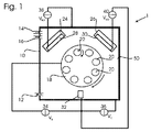
図1は、導電性の真空チャンバ壁50の内部を真空にするための真空システム12、及びスパッタリングガス(好ましくはアルゴン)及び反応ガス(好ましくは窒素)のためのインレット14,16を備えた真空チャンバ10を含むPDVスパッタコーティング(被覆)装置1を模式的に平面で示したものである。真空チャンバ10内において、遊星回転する支持体20を備えた回転可能な基材テーブル18が配置されている。図1において一つだけ示される基材ワークピース22が、支持体20の上に配置される。
FIG. 1 shows a
さらに、真空チャンバ10内には、回転テーブル18に隣接してマグネトロンカソード26,24が配置されている。各々のマグネトロンカソード24,26は、従来技術においてそれ自体が知られているように、非平衡マグネットシステムを含む。第一マグネトロンカソード24は、平らな矩形のスパッタリングターゲット28を含む。第二マグネトロンカソード26は、スパッタリングターゲット30を含む。
Further,
真空チャンバ10内には、アノード32が配置されている。アノード32は、異なる電源に電気的に接続される。バイアス電圧VBを発するためのバイアス電源34は、アノード32と基材テーブル18の間に接続され、基材テーブルは、バイアス電源34が個々の基材ワークピース22にも電気的に接続されるように、導電性を有する。バイアス電圧VBは、負、すなわち、基材の電位を負の値にして正電荷イオンを引き寄せる。
An
真空チャンバ壁電源36は、アノード32と真空チャンバ10の導電性の真空チャンバ壁50の間に接続されて、電圧Vcを発する。
A vacuum chamber
別個のアノード32を使用する代わりに、金属真空チャンバ壁50が、いくつかのアノードとして又は全てのカソードとして使用されてもよい。このように、代替の構成において、真空チャンバ壁電源36は存在しない。示される実施形態において、HIPIMS−カソード24(図1)、62a、62b(図8)および74a〜74d(図9)は、カソードとして真空チャンバ壁50に対し作動し、非HIPIMS−カソードは、専用のアノード32に対して作動する。別な方法として、専用のアノードに対してHIPIMS−カソードを作動させ、及び/又は真空チャンバ壁50に対して非HIPIMS−カソードを作動させることも可能である。
Instead of using a
第一マグネトロン電圧VM1を発する第一マグネトロン電源38は、第一マグネトロンカソード24と真空チャンバ壁50との間に接続されている。第二マグネトロン電圧VM2を発する第二マグネトロン電源40は、アノード32と第二マグネトロンカソード26との間に接続されている。以下に説明するように、第一電源38は、HIPIMS電源であり、ショートパルスで電力を供給する。HIPIMSマグネトロンカソード24及びそれに対応するHIPIMS電源38は、そのまま参考資料に組み込まれる、WO2009/132822A2において説明されているように、構成され駆動される。第二電源40は、従来のDC電源である。電源38,40は、アノード32に対して、カソード24,26に負電圧を供給する。
A first
コーティング(被覆)装置の操作において、基材22が回転支持体20上に載置される。真空チャンバ10内において真空が発生させられる。スパッタリングガスとしてアルゴンがインレット14から供給される。電力が電源38,40によりマグネトロンカソード24,26に印加され、真空チャンバ10内においてプラズマが発生させられる。
In the operation of the coating apparatus, the
プラズマからのイオンが、スパッタリングターゲット28,30をスパッタする。負のバイアス電圧VBを印加することで、プラズマからのイオンが、層を堆積させるための基材22の表面上に駆りたてられる(付勢される)。堆積工程の間中において、窒素が反応ガスとしてインレット16から供給される。
Ions from the plasma sputter the sputtering targets 28 and 30. By applying a negative bias voltage V B, ions from the plasma, (biased) is urged on the surface of the
図1に示すコーティング(被覆)装置において、第一及び第二マグネトロンカソード24,26は、それぞれのターゲット28,30の組成及び対応する電源38,40により供給される電力の両方を異にする。第一マグネトロンカソード24には、純粋な形態のAlターゲット28が備えられている。電源38は、HIPIMSによるパルスに電圧VM1、すなわち、ターゲット28で非常に高い電流密度の放電をもたらす非常に短いパルスを供給する。
In the coating apparatus shown in FIG. 1, the first and
第二マグネトロンターゲット26には、純粋な形態のTiターゲット30が備えられている。電力は、DC電圧VM1として第二マグネトロンカソード26に供給される。
The second magnetron target 26 is provided with a pure
本発明の第1実施形態において、Ti1−xAlxN膜は、図1の装置によって堆積される。そのような薄膜は、高温での高硬度および良好な耐酸化性を利点として、切断工具から航空宇宙産業の構成部品に至るまであらゆる種類の用途において摩耗保護のために使用されることが多い。立方TiNマトリックス内でAlの溶解度を高くさせ、ウルツ鉱AlNに構造的に分解させることなく準安定NaCl型の構造を形成する堆積方法は、高Al含有量が高温で被覆特性を改善するため、望まれている。 In the first embodiment of the present invention, the Ti 1-x Al x N film is deposited by the apparatus of FIG. Such thin films are often used for wear protection in all kinds of applications, from cutting tools to components in the aerospace industry, with the advantage of high hardness at high temperatures and good oxidation resistance. The deposition method that increases the solubility of Al in a cubic TiN matrix and forms a metastable NaCl-type structure without structural decomposition into wurtzite AlN, because the high Al content improves the coating properties at high temperatures, It is desired.
従来の直流マグネトロンスパッタリング(DCMS)において、単一相膜は、基材温度500℃で、x≦0.4の条件で典型的に得られる。他方、Alモル含有量が少なくともx=0.66までの固溶体は、カソードアーク蒸着により生成可能であるが、小滴(溶滴、droplets)が生じる。立方相で溶解可能なAlの量は、他の要因の間で、入射材料流束のイオン化にも依存するように思われる。これは、表面領域で起こるイオン衝撃誘導混合が、その系(system)を分解に駆り立てる化学的な力を効果的に超越し得るためである。 In conventional direct current magnetron sputtering (DCMS), a single phase film is typically obtained at a substrate temperature of 500 ° C. and x ≦ 0.4. On the other hand, solid solutions with an Al molar content of at least x = 0.66 can be produced by cathodic arc deposition, but droplets (droplets) are produced. The amount of Al that can be dissolved in the cubic phase appears to depend on the ionization of the incident material flux, among other factors. This is because ion bombardment induced mixing that occurs in the surface region can effectively transcend the chemical forces that drive the system to degradation.
この点において、高出力パルスマグネトロンスパッタリング(HIPIMS)は、DCMSよりもかなり高いスパッタ材料流束のイオン化が顕著であり、第1実施形態に適用され、この実施形態では、カソード24,26がハイブリッドHIPIMS−DCMS構成内で設けられる。元素アルミニウムターゲットが備えられた第一カソード24は、HIPIMSモードで作動、すなわち、高ピーク電流密度の放電を生じるパルスで作動し、一方、元素チタンターゲットを備えた第二カソード26は、DCMS操作にセットされ、すなわち、DC電源により電力が供給される。比較例においては、ターゲットを入れ替えて、Tiターゲットを有する電極がHIPIMSモードで操作され、さらにAlターゲットを有する電極がDCMSモードで操作される。このように、強烈な高エネルギー金属イオン流束の膜特性への影響は、Ti−およびAl−イオンで別々に検証される。
In this regard, high power pulsed magnetron sputtering (HIPIMS) has a significantly higher sputter material flux ionization than DCMS and is applied to the first embodiment, where the
第1実施形態によれば、Ti1−xAlxN膜の堆積は、図1に示す被覆システムで行われる。第一試験では、ケイ素基材(基板)が被覆特性を検証するために使われる。しかしながら、好ましい実施例では、工具基材22が被覆され、すなわち、超硬合金の切刃インサートが基材22として設置される。
According to the first embodiment, the Ti 1-x Al x N film is deposited by the coating system shown in FIG. In the first test, a silicon substrate (substrate) is used to verify the coating properties. However, in the preferred embodiment, the
実施例および比較例の両方において、被膜内のAl含有量は、HIPIMS電力を一定に維持しつつ、DCMS操作のカソード上で平均電力を変えることで制御される。Al−HIPIMS/Ti−DCMS構成を有する実施例では、第一電極24でのHIPIMS平均電力は、2.5kW(5J/パルス、500Hz、反応モードのアーク放電により制限され、10%デューティサイクル)に固定され、第二電極26でのDCMS電力は、Al含有量が0.4≦x≦0.76となるよう、1.4kWと4kWの間で調整される。比較例では、TiおよびAlターゲットは、電極24,26の間で取り替えられる。その結果生じるTi−HIPIMS/Al−DCMS設定では、高平均HIPIMS電力5kW(10J/パルス、500Hz、10%デューティサイクル)が、所望の組成範囲で膜を成長させるために必要であるが、これはTiスパッタ速度がAl速度の約半分であるためである。第二電極26でのDCMS電力は、Alターゲットを備えた比較例において、0.75kW(x=0.41)から3kW(x=0.83)まで変化させられる。
In both the examples and comparative examples, the Al content in the coating is controlled by varying the average power on the cathode of the DCMS operation while keeping the HIPIMS power constant. In an embodiment with an Al-HIPIMS / Ti-DCMS configuration, the HIPIMS average power at the
実施例および比較例両方において、負のDCバイアス電圧VBとして60Vが使用される。N2対Arの流速比は0.2に固定され、その結果生じるプロセス圧力は0.4Paとなる。さらに、2×10kW(2時間以上の加熱フェーズ)および2×8kW(コーティングフェーズ、通常は90分以上)の輻射加熱(不図示)が使用される。 In the examples and comparative examples both, 60V is used as a negative DC bias voltage V B. The flow rate ratio of N 2 to Ar is fixed at 0.2 and the resulting process pressure is 0.4 Pa. In addition, radiant heating (not shown) of 2 × 10 kW (heating phase of 2 hours or more) and 2 × 8 kW (coating phase, usually 90 minutes or more) is used.
被覆工程の間中、Al−HIPIMS/Ti−DCMS構成を有する実施形態によれば、ピーク電流密度、すなわち、ターゲット28の前面で分割される第一電極24に供給される電流は、0.39A/cm2であり、それ故に、同じ大きさの第二ターゲット30での(一定の)電流密度≦0.022A/cm2よりもかなり高い。同じ大きさのターゲットを有する比較例において、HIPIMSで駆動されるチタンターゲットでの電流密度は、ピーク時で1.14A/cm2である。
Throughout the coating process, according to an embodiment having an Al-HIPIMS / Ti-DCMS configuration, the peak current density, i.e. the current supplied to the
堆積中における基材22の温度は、〜500℃であることが見い出される。
The temperature of the
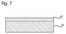
図7は、基材(基板)22上に設けた被覆層52を模式的に示したものである。ターゲット電力比、すなわち、DCMSモードで第二マグネトロン26に供給される(一定の)電力により分割されるHIPIMSモードで操作される第一カソード24に供給される(時間平均)ターゲット電力に応じて、被覆組成に変化が見られた。
FIG. 7 schematically shows the
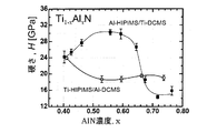
図2は、試験に供される両方のターゲット配列のDC電力を関数とする膜内のAlN含有量を示す。図より、HIPIMSの適用によって、スパッタ収量の差異から予想される傾向との間に大きな偏差を生じる。TiターゲットがHIPIMSモード(白丸表示)で駆動されると、予想されるAl含有量より高い被膜が得られる。類似性の観点より、HIPIMSがAlターゲット(黒四角表示)に適用されると、膜内のAl含有量は減少する。 FIG. 2 shows the AlN content in the film as a function of DC power for both target arrays subjected to the test. From the figure, application of HIPIMS causes a large deviation from the expected trend from the difference in sputter yield. When the Ti target is driven in HIPIMS mode (white circle display), a coating higher than the expected Al content is obtained. From the viewpoint of similarity, when HIPIMS is applied to an Al target (black square display), the Al content in the film decreases.
図3において、ナノ押込硬度は、実施例および比較例の両方において、膜内のAl含有量を関数とするすべてのTi1−xAlxN被膜を対象にプロットされる。特筆すべきは、HIPIMSのTi又はAlターゲットへの適用が、機械的特性に劇的な結果をもたらすことである。x=0.4の開始点において、非常に類似の硬度24GPaが両方の構成で得られるが、Al濃度が増加するにつれてデータの発散が見られる。Al−HIPIMS/Ti−DCMS構成を有する実施例において、硬度は、Al含有量の増加とともに増加し、0.55≦x≦0.6で最大値30GPaに到達するが、x>0.65で極端に減少する。 In FIG. 3, nanoindentation hardness is plotted for all Ti 1-x Al x N coatings as a function of Al content in the film in both the examples and comparative examples. It should be noted that the application of HIPIMS to Ti or Al targets has dramatic results in mechanical properties. At the starting point of x = 0.4, a very similar hardness of 24 GPa is obtained with both configurations, but data divergence is seen as the Al concentration increases. In an example with an Al-HIPIMS / Ti-DCMS configuration, the hardness increases with increasing Al content and reaches a maximum value of 30 GPa with 0.55 ≦ x ≦ 0.6, but with x> 0.65 Extremely decreases.
それと対照的に、Ti−HIPIMS/Al−DCMS構成を有する比較例においては、x=0.53ですでに硬度が18.5Gpaまで減少し、高Al濃度を有する膜でも硬度は低い値のままである。両方法とも、x=0.67になって、再び同じ硬度を示している。 In contrast, in the comparative example having the Ti-HIPIMS / Al-DCMS configuration, the hardness is already reduced to 18.5 Gpa at x = 0.53, and the hardness remains low even with the film having a high Al concentration. It is. In both methods, x = 0.67, indicating the same hardness again.
この結果、組成範囲0.55≦x≦0.6において、強烈なAlイオン衝撃下で実施例により作成される膜は、HIPIMS電源からTiイオンのエネルギー流束に周期的に曝される比較例によって作成される膜よりも〜65%(最大で65%)硬い。 As a result, in the composition range 0.55 ≦ x ≦ 0.6, the films prepared according to the examples under intense Al ion bombardment are periodically exposed to the energy flux of Ti ions from the HIPIMS power source. ~ 65% (up to 65%) harder than the film made by
膜のXDR解析(結晶面がサンプル表面に平行でなくても、六方晶系の粒子の電位の存在を検知するために、傾斜角を0℃と75℃の間で変化させる一連のΘ−2Θスキャン)では、比較例の膜(Ti−HIPIMS/Al−DCMS構成)において、0.41≦x≦0.53の範囲で、立方Ti1−xAlxN相のみが示されることが認められる。六方晶系のAlN充足(リッチ)相は、Ti0.4Al0.6NサンプルにおいてXRDにより最初に検知される。六方晶系および立方相の含有量間の相対比率は、Al濃度の増加とともに増加し、最終的にx=0.74で、立方相はXRDで検知不能になる。他方、代わりにHIPIMSがAlターゲットで使用されれば(Al−HIPIMS/Ti−DCMS)、溶解度上限は、このシリーズからTi0.41Al0.59N膜が立方相のみを示す事実から例示されるように、明らかに高い。このターゲット構成における六方晶系相はx=0.65で最初に検知され、合金分解の開始が0.59≦x≦0.65の範囲に、すなわち、混合エントロピー(すなわち分解の化学的な原動力)が最大値に達する領域にあることが示される。(このシリーズで)x=0.77の最大Al含有量を有するサンプルにおいて、立方相は、Tiターゲット上のHIPIMSで作成されるサンプルとは対照的に、(六方晶系相と共存する)XRDにより、いまだに明確に検知され得る。 XDR analysis of the film (a series of Θ-2Θ varying the tilt angle between 0 ° C and 75 ° C in order to detect the presence of hexagonal grain potential even if the crystal plane is not parallel to the sample surface. In the scan), in the film of the comparative example (Ti-HIPIMS / Al-DCMS configuration), it is recognized that only the cubic Ti 1-x Al x N phase is shown in the range of 0.41 ≦ x ≦ 0.53. . A hexagonal AlN-satisfied (rich) phase is first detected by XRD in a Ti0.4Al0.6N sample. The relative ratio between hexagonal and cubic phase content increases with increasing Al concentration, finally x = 0.74 and the cubic phase becomes undetectable by XRD. On the other hand, if HIPIMS is used instead with an Al target (Al-HIPIMS / Ti-DCMS), the solubility upper limit, as exemplified by the fact that Ti0.41Al0.59N films from this series show only cubic phase, Obviously high. The hexagonal phase in this target configuration was first detected at x = 0.65 and the onset of alloy decomposition was in the range 0.59 ≦ x ≦ 0.65, ie, mixed entropy (ie, the chemical motive force of decomposition). ) Is in the region where the maximum value is reached. In the sample with the maximum Al content of x = 0.77 (in this series), the cubic phase is XRD (coexisting with the hexagonal phase) as opposed to the sample made with HIPIMS on the Ti target. Can still be clearly detected.
Al含有量を関数とする好ましい配向の変化(進展)は、図4に示すように、明らかにターゲット構成に依存する。実施例(Al−HIPIMS/Ti−DCMS)から得られる膜は、テクスチャーがない(x=0.59)方向に徐々に変化する低Al含有量(0.40≦x≦0.56)で(111)テクスチャーを示し、最終的に高Al濃度で(200)−テクスチャーに成る。逆の傾向が、比較例(Ti−HIPIMS/Al−DCMS構成)によって作成されるサンプルで観察される。最小Al含有量を有する膜は、最大の(200)配向を示し、テクスチャーがない方向へ徐々に変化する。六方晶系相からの信号と重なるため、このシリーズでの膜で、x>0.6において、膜のテクスチャーを信頼性を持って決定することはできなかった。 The preferred orientation change (development) as a function of Al content clearly depends on the target configuration, as shown in FIG. The film obtained from the example (Al-HIPIMS / Ti-DCMS) has a low Al content (0.40 ≦ x ≦ 0.56) that gradually changes in the direction without texture (x = 0.59) ( 111) shows texture and finally becomes (200) -texture with high Al concentration. The reverse trend is observed in the sample made by the comparative example (Ti-HIPIMS / Al-DCMS configuration). The film with the minimum Al content shows the maximum (200) orientation and gradually changes in the direction without texture. Because of the overlap with the signal from the hexagonal phase, the film texture could not be determined reliably with x> 0.6 for films in this series.
図5a〜5dは、最も代表的なサンプルの分析的なTEM特性を示す。 Figures 5a-5d show the analytical TEM characteristics of the most representative samples.
図5a〜bは、TI0.6Al0.4NおよびTi0.41Al0.59Nの組成を備えた実施例(Al−HIPIMS/Ti−DCMS構成)により堆積される膜のTEM画像の概要を示す。 FIGS. 5a-b show a summary of TEM images of films deposited by an example (Al-HIPIMS / Ti-DCMS configuration) with a composition of TI0.6Al0.4N and Ti0.41Al0.59N.
図5c〜dは、比較例(Ti−HIPIMS/Al−DCMS構成)、すなわち、TI0.59Al0.41NおよびTi0.47Al0.53Nを備えた二つの膜で提供されるTEMサンプルを示す。 Figures 5c-d show a TEM sample provided in a comparative example (Ti-HIPIMS / Al-DCMS configuration), i.e. two films with TI0.59Al0.41N and Ti0.47Al0.53N.
すべてのサンプルは、カラム(円柱)径が約20〜40nmの稠密な柱状構造を有する。Al含有量がx=0.59であるAl−HIPIMS/Ti−DCMSサンプルは、他よりも少し微細な粒子を有する。インサート(inserts)内に対応する制限視野電子回折(SAED)パターンでは、x=0.4での実施例によるサンプルが強烈な<111>テクスチャーを有する一方、上記のXRD結果にしたがい、類似のAl含有量(x=0.41)を有する比較例の膜が<200>−テクスチャーをもたらす、ことが明らかにされる。高Al含有量(図5bおよび5d)を有する膜は両方とも、ほぼテクスチャーが見られない。いくつかのサンプルにおいて、少数の相が矢印で示されるように認められた。 All samples have a dense columnar structure with a column (cylinder) diameter of about 20-40 nm. The Al-HIPIMS / Ti-DCMS sample with Al content x = 0.59 has slightly finer particles than the others. In the corresponding limited field electron diffraction (SAED) pattern in the inserts, the sample according to the example at x = 0.4 has a strong <111> texture, whereas according to the above XRD results, a similar Al It is revealed that the comparative film having a content (x = 0.41) results in a <200> -texture. Both films with high Al content (FIGS. 5b and 5d) are almost untextured. In some samples, a small number of phases were observed as indicated by the arrows.
実施例にしたがって作成したサンプルにおいて、図6はアニール試験の結果を示す。高Al含有量(x=0.59)を有するサンプルは、時効硬化を経て、900℃で最大硬度33GPaに達する。それに対し、低Al含有量(不図示)を有するサンプルでは、硬度は温度上昇とともに悪化する。900℃でアニール処理されたサンプルを用いて行われた傾斜角依存のXRD(不図示)により、Ti0.60Al0.40Nサンプルの場合で、六方晶系相の存在が示された。後者はまた、900℃でのアニール処理の後、Ti0.41Al0.59Nサンプルの場合に検知された。しかしながら、この場合は、かなりの非対称性の回折ピークにより、特に傾斜角が大きい箇所で、主に表面領域内で立方AlN相の形成が示された。 For the samples made according to the examples, FIG. 6 shows the results of the annealing test. A sample with a high Al content (x = 0.59) undergoes age hardening and reaches a maximum hardness of 33 GPa at 900 ° C. On the other hand, in samples having a low Al content (not shown), the hardness deteriorates with increasing temperature. The tilt-dependent XRD (not shown) performed using the sample annealed at 900 ° C. showed the presence of a hexagonal phase in the case of the Ti0.60Al0.40N sample. The latter was also detected in the case of Ti0.41Al0.59N sample after annealing at 900 ° C. However, in this case, the formation of a cubic AlN phase mainly in the surface region was shown by the considerably asymmetric diffraction peak, particularly at the location where the tilt angle was large.
図11は、アニール処理がXRDピークにどのように影響するかを示し、それ故にスピノーダル分解を例示する。Θ−2ΘXRD測定は、900℃でアニール処理されたTi0.41Al0.59NAl−HIPIMS/Ti−DCMS膜で傾斜角Ψを関数として実施されており、立方相からの111および002の回折ピークが、特に大きな傾斜角においてかなり非対称であることが示され、立方AlN相が主に表面近傍領域で存在することが示唆される。
一つの実施例が、図11において、膜形成直後のサンプルの対応データとともに示される。立方AlN相から付加的な寄与(addtional contribution)により生じる非対称性の他に、アニール処理後のサンプルからの回折ピークが回折角度を低下させるよう移行し、TiN相の回折角度に近づくことは注目に値し、スピノーダル分解反応経路c−(Ti,Al)N→c−TiN+c−AlNが確認される。
FIG. 11 shows how the annealing process affects the XRD peak and therefore illustrates spinodal decomposition. Θ-2ΘXRD measurements have been performed on Ti 0.41 Al 0.59 NAl-HIPIMS / Ti-DCMS films annealed at 900 ° C. as a function of tilt angle Ψ, and 111 and 002 diffraction from the cubic phase. The peak is shown to be fairly asymmetric, especially at large tilt angles, suggesting that the cubic AlN phase exists mainly in the near-surface region.
One example is shown in FIG. 11 with corresponding data for a sample immediately after film formation. In addition to the asymmetry caused by the additional contribution from the cubic AlN phase, it is noteworthy that the diffraction peak from the annealed sample shifts to reduce the diffraction angle and approaches the diffraction angle of the TiN phase. The spinodal decomposition reaction path c- (Ti, Al) N → c-TiN + c-AlN is confirmed.
要約すると、実施例では、DCMSまたはカソードアーク等の他のスパッタリング技術に比べて、HIPIMS処理はターゲットの組成/構成に基づき予測可能な膜の化学量論に結びつかない、ことが示される。この特異的な挙動は、HIPIMSにおける電力が正規化(規格化)された堆積速度が一般的にDCMSの場合より低く、堆積速度の損失が元素に特有である、という事実により生じる。 In summary, the examples show that HIPIMS treatment does not lead to predictable film stoichiometry based on target composition / configuration compared to other sputtering techniques such as DCMS or cathodic arc. This specific behavior arises from the fact that the power normalized deposition rate in HIPIMS is generally lower than in DCMS, and the deposition rate loss is specific to the element.
ここで述べられた結果は、強力なAl又はTiイオン流束の膜特性に与える影響間の劇的な非対称性を示し、それらはAl濃度の増加とともに生じる膜硬度の進展により最適に例示される(図3参考)。 The results described here show a dramatic asymmetry between the effects of strong Al or Ti ion flux on the film properties, which are best exemplified by the development of film hardness that occurs with increasing Al concentration. (See Figure 3).
結論として、DCMS又はHIPIMSモードのいずれかで駆動されるターゲットから発せられるイオン流束の明らかに異なる組成により、結果として生じる膜の特性に与えるAl + およびTi + のイオン流束の影響は、かなり異なる。実施例(Al−HIPIMS/Ti−DCMSターゲット構成)によるAl + を用いた衝撃により、高硬度(>30GPa)および低残留応力を示す高Al含有(0.55≦x≦0.6)膜を堆積することが可能になる。 In conclusion, the distinctly different composition of the ion flux emitted from the target to be driven in either DCMS or HIPIMS mode, the effect of ion flux of Al + and Ti + gives the characteristics of the film resulting considerable Different. High Al content (0.55 ≦ x ≦ 0.6) film showing high hardness (> 30 GPa) and low residual stress by impact with Al + according to the example (Al-HIPIMS / Ti-DCMS target configuration). It becomes possible to deposit.
比較例によれば、Ti + 金属イオン流束、特にTi2+イオン流束(Ti−HIPIMS/Al−DCMS構成)を用いて作成される対応するAl含有量を有する被膜は、18〜19GPaの範囲の硬度を示す。同様な組成を有する膜でのこのように異なる機械的特性は、TiNマトリックス内のAl溶解度が使用されるターゲット構成に強く依存するという事実に起因する。得られた結果により、最大40at%のAlが、成長過程でAl−HIPIMSマグネトロンからAl−イオンのサポートを受ける場合の64at%Alと比較して、Ti−HIPIMSマグネトロンから発せられるTiイオン流束を用いる立方相内に適応し得ることが示唆される。 According to the comparative example, the coating with the corresponding Al content made using Ti + metal ion flux, in particular Ti2 + ion flux (Ti-HIPIMS / Al-DCMS configuration), is in the range of 18-19 GPa The hardness is shown. Such different mechanical properties in films with similar compositions are due to the fact that the Al solubility in the TiN matrix is strongly dependent on the target configuration used. The results obtained show that a Ti ion flux emanating from a Ti-HIPIMS magnetron is up to 40 at% Al compared to 64 at% Al when receiving Al-ion support from an Al-HIPIMS magnetron during the growth process. It is suggested that it can be adapted within the cubic phase used.
アノード32および層52が堆積される基材22の間に印加されるバイアス電圧VBは、DC電圧またはパルスで印加される。特筆すべきは、層52の構造及び特性が、バイアス電圧VBの大きさおよび第一マグネトロンカソード24に印加されるHIPIMSパルスでパルスバイアス電圧VBの同期をとることの両方を特異的に選択することで、かなり影響される。再び特筆すべきは、入れ替えられたターゲット構成を有する比較例とは対照的に、第一カソード24に設けられるアルミニウムターゲット28の好ましい実施例と第二のDC駆動カソード26に設けられるTiターゲット30との間で、際立った違いが見出される。
The bias voltage V B applied between the
図12は、電圧パルスVM1を第一カソード24に印加することにより、可能なパルス形状の一例であるHIPIMSパルスがt=0μsで開始された後に現れる、個々のタイプのイオンのエネルギー合成イオン総数を決定する、原位置(その場)時間分解イオン質量分光法の結果をグラフに示したものである。図12から明らかなように、HIPIMSパルスの3つの区別されるフェーズ(相)42,44および46が画定される。最初の期間42では、パルスの開始後約0〜40μsで示される例において、プラズマ中のイオンは、金属イオンから比較的低い寄与(low contribution)を有するAr+イオンが支配的となる。
金属イオンの充足期間44に該当する次に続く期間では、約40〜100μsで現れる図12の例において、プラズマは金属イオンが支配的となる。金属イオンの充足期間44において、ガスイオンの強度は希薄化のため減少する。続いて、後の金属相46では、100μsから始まる本実施例において、プラズマは、熱運動化(熱平衡化)された金属イオンが存在すると共に、熱運動化(熱平衡化)されたArイオンが支配的となる。
FIG. 12 shows the total number of energetic ions of individual types of ions that appear after applying a voltage pulse V M1 to the
In the following period corresponding to the metal
このように、各々のHIPIMSパルス内で時間経過とともに異なる期間内では、異なるタイプのイオンが存在する。DC電圧として連続的に印加されるバイアス電圧VB、又は、HIPIMSパルスと完全に同期された、すなわちt=0μsでのその開始から現れるパルスバイアス電圧VBにより、すべての3つのフェーズ(相)42,44,46から発するイオンは、基材22に作用する。しかしながら、上記の期間のうち選択された一つ(の期間)のみと同期するパルスバイアス電圧VBを与えることにより、プラズマから発するイオンのグループを選択して、成長する層52に作用させることが可能である。
Thus, there are different types of ions within different periods of time within each HIPIMS pulse. All three phases with a bias voltage V B applied continuously as a DC voltage, or with a pulse bias voltage V B appearing fully synchronized with the HIPIMS pulse, ie starting from its start at t = 0 μs Ions emitted from 42, 44, 46 act on the
特に、図12に示される、金属イオンが支配的な、金属イオンの充足期間44とバイアスパルスを十分に同期させることにより、これらのイオンを特異的に選択して、それによって、本事例のArにおいて、そのプロセスガスのイオンにより生じる影響を最小限にすることが可能である。
In particular, these ions are specifically selected by fully synchronizing the metal
図13は、第一カソード24に供給される単一のHIPIMSパルスの例に対する、電圧VM1の曲線、第一カソード24での電流IM1、及び同期パルスバイアス電圧VBを示す。
FIG. 13 shows the curve of voltage V M1 , current I M1 at
当業者に認識されるように、電圧VM1及びVB、及び電流IM1の大きさは、図13に示されていない。HIPIMSパルスのため、電圧VM1は、約2000Vのピーク値まで上昇し、電流IM1は、約3000Aのピーク値(100%)に到達する。電圧VM1およびVBは、同じスケールで示されていない。 As will be appreciated by those skilled in the art, the magnitudes of voltages V M1 and V B and current I M1 are not shown in FIG. Due to the HIPIMS pulse, the voltage V M1 rises to a peak value of about 2000V and the current I M1 reaches a peak value (100%) of about 3000A. Voltages V M1 and V B are not shown on the same scale.
パルス電圧VM1は、t=0〜200μsから印加される。その結果生じる電流IM1もまたパルス挙動を示す。電流のパルス持続時間(幅)Tは、電流IM1が最大電流値の5%を上回る期間(時間)と定義され、約200μsである。 The pulse voltage V M1 is applied from t = 0 to 200 μs. The resulting current I M1 also exhibits pulse behavior. The pulse duration (width) T of the current is defined as the period (time) in which the current I M1 exceeds 5% of the maximum current value, and is about 200 μs.
示された実施例において、バイアス電圧VB は、持続時間(幅)TBの電圧パルスとして印加され、本実施例ではTB=70μsであり、TBはTの約30%である。バイアスパルスは、遅延時間TDの後に印加され、本実施例では40μs、すなわち、パルス持続時間Tの約20%に対応する。 In the example shown, the bias voltage V B is applied as a voltage pulse of duration (width) T B , in this example T B = 70 μs, and T B is about 30% of T. Bias pulse is applied after a delay time T D, in this embodiment 40 [mu] s, i.e., corresponding to approximately 20% of the pulse duration T.
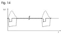
図14は、バイアスパルスが各々のHIPIMSパルスとどのように同期されるかを示す。示された実施例では、約200μsの持続時間(幅)を有するHIPIMSパルスが、周波数400Hzで、すなわち、約2500μsのインターバル(間隔)で、すなわち4%のデューティサイクル(負荷サイクル)で出現する。各々のHIPIMSパルスのインターバルにおいて、バイアスパルスは同じ持続時間であり、パルスの開始後に同じ遅延時間TDで出現する。 FIG. 14 shows how the bias pulse is synchronized with each HIPIMS pulse. In the example shown, HIPIMS pulses with a duration (width) of about 200 μs appear at a frequency of 400 Hz, ie at an interval of about 2500 μs, ie with a 4% duty cycle (duty cycle). In each of the HIPIMS pulse interval, the bias pulse is the same duration, appearing after the start of the pulse at the same delay time T D.
このように規定されるバイアスパルスは、金属イオンの充足期間44に対応する。同期は完全である必要はなく、他の期間と例えば10%程度の少ない重なりがあっても良好な結果が得られる、ということが、当業者により認識される。
The bias pulse thus defined corresponds to the metal ion
DCバイアス、HIPIMSパルス(0〜200μs)に完全に同期するバイアスパルスを有するパルスバイアス、及び金属イオンの充足期間44(HIPIMSパルス開始後の40〜100μs)に限定される図13に示される好ましいバイアスパルスの比較において、好ましい短いバイアスパルスを用いて堆積された膜52は、その膜内に取り込まれた非常に低濃度のArを有し、検出限界以下であり、一方、DCバイアスおよび完全に同期するパルスバイアスは、その膜内に混入されたアルゴンの量が多いことを示す。好ましい短いパルスは、堆積した単一相のNaCl構造を有する層を生成し、稠密な柱状微細構造を示す。
対照的に、連続するDC又は完全に同期するバイアスは、二相構造の傾向を示し、Ar混入及び反跳注入に起因して、比較的高濃度の取り込まれたAr及び高残留圧縮応力を有する、立方TiN及びウルツ鉱AlNの混合物を含む、膜へと導く。さらに、リスパッタリングは、金属イオンの充足期間に同期するバイアスパルスの場合に低くなり、堆積速度は増加する。
The preferred bias shown in FIG. 13 limited to a DC bias, a pulse bias with a bias pulse that is fully synchronized with the HIPIMS pulse (0-200 μs), and a metal ion sufficiency period 44 (40-100 μs after the start of the HIPIMS pulse). In the pulse comparison, the
In contrast, continuous DC or fully synchronous biases show a tendency to a two-phase structure, with relatively high concentrations of Ar and high residual compressive stress due to Ar incorporation and recoil injection To a film containing a mixture of cubic TiN and wurtzite AlN. Furthermore, resputtering is lower for bias pulses that are synchronized to the metal ion sufficiency period and the deposition rate is increased.
言及されるべきことは、図13に示されるようなHIPIMSパルスのパルス形状は、そのようなパルスの一例に過ぎない、ということである。HIPIMSカソードのためのHIPIMS電源において、パルスは、カソードに荷電したコンデンサを接続することにより好ましく得られ、コンデンサはカソードとアノードの間のギャップを渡って放電する。コンデンサが十分に放電されると、図13に描写されたようなパルス形状が発生する。 It should be mentioned that the pulse shape of the HIPIMS pulse as shown in FIG. 13 is only one example of such a pulse. In a HIPIMS power supply for a HIPIMS cathode, the pulses are preferably obtained by connecting a charged capacitor to the cathode, which discharges across the gap between the cathode and anode. When the capacitor is fully discharged, a pulse shape as depicted in FIG. 13 occurs.
しかしながら、そのパルス形状は、変更されてもよい。特に、HIPIMSパルスの持続時間を減少させるのが好まれる。図12に示されるように、金属イオンの充足期間は、パルス開始後に約100μsまで続く。したがって、例えば100μsのような特定時間の後に、パルスをカット(遮断)する(すなわち、コンデンサの接続を断つ)ことが有利である。これにより、後の期間46で作動ガスのイオンが高濃度になるのを回避しつつ、有利な金属イオンの充足期間44を得ることが可能になる。さらに“カット(遮断)”(すなわち、強制終了)パルスは、HIPIMSカソードで自己スパッタリングが少ない利点を有する。
However, the pulse shape may be changed. In particular, it is preferred to reduce the duration of the HIPIMS pulse. As shown in FIG. 12, the metal ion sufficiency period continues to about 100 μs after the start of the pulse. Therefore, it is advantageous to cut (cut off) the pulse (ie disconnect the capacitor) after a certain time, eg 100 μs. This makes it possible to obtain an advantageous metal ion
特に好ましいのは、同期バイアスパルスと、カットすなわち短縮化されたHIPIMSパルスの組み合わせである。HIPIMSパルスは、金属イオン(図12のAl−イオンを参照)の増加の原因である雪崩効果が一度生じると、HIPIMSカソードの前にイオン雲を生成する結果を得る。HIPIMSパルス(例えば、10〜50μs)の開始後に遅延をもって開始し、又、金属イオンの充足期間44に同期して印加されるがその後に供給される同期バイアスパルスは、HIPIMSカソードの前に形成されるイオン雲を基材上に加速する結果を得る。
Particularly preferred is a combination of a synchronous bias pulse and a cut or shortened HIPIMS pulse. The HIPIMS pulse produces the result of creating an ion cloud in front of the HIPIMS cathode once the avalanche effect, which causes an increase in metal ions (see Al-ions in FIG. 12), occurs. A synchronous bias pulse that starts with a delay after the start of the HIPIMS pulse (eg, 10-50 μs) and is applied in synchronization with the metal
図15に示すように、バイアスパルスの大きさは、Å(オングストローム)を単位とする格子定数a0に影響を与える。(パルス)バイアス電圧VB<120Vに対して、格子定数a0はアルミニウム含有量x=0.62において予想されるより小さく、一方、VB>120Vで作成される膜は予想されるより高いa0を示す。第一(HIPIMS)電極に設けられたチタンターゲットを有する比較例では、低バイアス電圧ですでに、際立った変動を有する異なる挙動を示す。 As shown in FIG. 15, the magnitude of the bias pulse affects the lattice constant a 0 in units of Å (angstrom). For (pulse) bias voltage V B <120V, the lattice constant a 0 is smaller than expected at aluminum content x = 0.62, while films made with V B > 120V are higher than expected. a 0 is shown. The comparative example with a titanium target provided on the first (HIPIMS) electrode already exhibits different behavior with significant variations at low bias voltages.
図16は、GPaを単位とする残留応力σを示す。図示されるように、層は、VS≦160Vで低残留応力を示す。VS>200Vにおいて、圧縮応力は、−1GPaよりも大きい。対照的に、比較例では、膜は、低バイアス電圧でも高圧縮応力を示す。 FIG. 16 shows the residual stress σ in units of GPa. As shown, the layer exhibits low residual stress with V S ≦ 160V. For V S > 200V, the compressive stress is greater than −1 GPa. In contrast, in the comparative example, the film exhibits high compressive stress even at low bias voltage.
図17は、バイアス電圧VBの大きさがGPaを単位とする押込硬さに与える顕著な影響を示す。HIPIMS電極24に設けられたアルミニウムターゲットを有する好ましい実施例において、膜の硬さは、VBの増加とともに増加し、120V≦VB≦160Vの区間において、約30GPaに到達する。HIPIMS電極24に設けられたチタンターゲットを有する比較例においては、硬さは、かなり低く、20GPaを超えない。
FIG. 17 shows the remarkable influence that the magnitude of the bias voltage V B has on the indentation hardness in GPa. In the preferred embodiment having an aluminum target provided
結果として、好ましいバイアス電圧VBは、金属イオンの充足相44と同期する持続時間で、−80−140Vの大きさのパルス、すなわち、実施例ではt=40μsからt=100μsまでの範囲で供給される。
As a result, the preferred bias voltage V B is supplied with a pulse duration of −80-140 V, ie, in the example from t = 40 μs to t = 100 μs, with a duration synchronized with the metal
図18は、Ti−Al−N層で被覆された基材上で行う摩耗試験の評価を示す。 FIG. 18 shows the evaluation of an abrasion test performed on a substrate coated with a Ti—Al—N layer.
異なるバイアスで得られる被膜において、被膜表面上で摩耗部材の通過(パス)数に対する最大摩耗幅VBmaxが示される。実線表示の曲線Aは、Ti−HIPIMS/Al−DCMS電極構成で得られる比較例に対応するものであり、特に28通過(パス)後はかなりの程度の摩耗を示している。 For coatings obtained at different biases, the maximum wear width VB max is shown versus the number of wear member passes on the coating surface. A curve A indicated by a solid line corresponds to a comparative example obtained with a Ti-HIPIMS / Al-DCMS electrode configuration, and shows a considerable degree of wear, particularly after 28 passes.
点線表示の曲線Bは、HIPIMSパルスの完全な0〜200μsの継続時間で同期する、−60Vパルスバイアスを有するAl−HIPIMS/Ti−DC電極構成で得られる被膜に対応するものである。このサンプルは、曲線C(DCバイアスを用いるAl−HIPIMS/Ti−DC、一点鎖線表示)と同様に、比較例よりも改善した摩耗挙動を示している。 Dotted curve B corresponds to the coating obtained with an Al-HIPIMS / Ti-DC electrode configuration with a -60 V pulse bias that synchronizes with a complete 0-200 [mu] s duration of the HIPIMS pulse. Similar to curve C (Al-HIPIMS / Ti-DC using DC bias, one-dot chain line display), this sample shows improved wear behavior over the comparative example.
最小摩耗幅が、曲線Dで得られ、各々のHIPIMSパルスの開始後に40〜100μsの金属イオン充足期間にのみ同期する、−120Vパルスバイアスを有するAl−HIPIMS/Ti−DC電極構成で得られる被膜に対応するものである。 Coating obtained with an Al-HIPIMS / Ti-DC electrode configuration with a -120 V pulse bias, with a minimum wear width obtained on curve D, synchronized only to the 40-100 μs metal ion sufficiency period after the start of each HIPIMS pulse It corresponds to.
二つより多くの電極をもたない図1に係るコーティング(被覆)装置の第1実施形態は、基材22上に被膜52を形成するために使用されるが、工業的規模において、基材22を被覆(コーティング)するための装置に、二つ以上のカソードを設けることが好ましい。
The first embodiment of the coating apparatus according to FIG. 1 without more than two electrodes is used to form the
第2実施形態として、図8は、図1のコーティング(被覆)装置に対応するが、異なる電極構成を有するコーティング(被覆)装置60を示す。同様に、図9は、第3実施形態を示す。電極構成、すなわち、カソードに設けられるターゲットはもちろん電源のタイプおよび配置を除き、図8及び9のコーティング(被覆)装置は、図1に示される第1実施形態と同じである。特に、バイアス電源は、明瞭性のみを理由に、図8及び図9では省略されている。
As a second embodiment, FIG. 8 shows a
図8に係る第2実施形態において、4つの従来のDC駆動マグネトロンカソード66a,66b,66c,66dが、チャンバ10内に設けられ、それぞれが、アノード32に接続されたDC電源68a,68b,68c,68dを備えている。二つのHIPIMSカソード62a,62bが設けられ、それぞれが、真空チャンバ壁50に接続されたHIPIMS電源64a,64bを備えている。
In the second embodiment according to FIG. 8, four conventional DC driven
以下に、図8,図9の実施形態におけるターゲット構成の実施例および対応する操作について述べる。そのような構成の実施例が以下の表に列挙され、6つのカソードそれぞれに対して、ターゲット材料および操作タイプ(DC又はH=HIPIMS)が示される。 Hereinafter, examples of target configurations and corresponding operations in the embodiments of FIGS. 8 and 9 will be described. Examples of such configurations are listed in the table below, and for each of the six cathodes, the target material and operation type (DC or H = HIPIMS) are shown.
実施例1 実施例2 実施例3
構成 図8 図8 図8
62a:AlSi−H 62a:Al−H 62a:Al−H
62b:Cr−H 62b:Cr−H 62b:Al−H
66a:TiAl−DC 66a:TiAl−DC 66a:Ti−DC
66b:TiAl−DC 66b:TiAl−DC 66b:Al−DC
66c:TiAl−DC 66c:TiSi−DC 66c:Ti−DC
66d:TiAl−DC 66d:TiSi−DC 66d:TiAl−DC
Example 1 Example 2 Example 3
Configuration FIG.
62a: AlSi-H 62a: Al-H 62a: Al-H
62b: Cr—
66a: TiAl-DC 66a: TiAl-DC 66a: Ti-DC
66b: TiAl-DC 66b: TiAl-DC 66b: Al-DC
66c: TiAl-DC 66c: TiSi-DC 66c: Ti-DC
66d: TiAl-
実施例4 実施例5 実施例6
構成 図9 図8 図8
76a:TiAl−DC 62a:Al−H 62a:Al−H
76b:TiAl−DC 62b:Cr−H 62b:Cr−H
72a:Cr−H 66a:TiAl−DC 66a:TiAl−DC
72b:AlSi−H 66b:TiAl−DC 66b:TiAl−DC
72c:Al−H 66c:TiAl−DC 66c:Ti−DC
72d:AlSi−H 66d:TiAl−DC 66d:TiAl−DC
Example 4 Example 5 Example 6
Configuration FIG.
76a: TiAl-DC 62a: Al-H 62a: Al-H
76b: TiAl-
72a: Cr-H 66a: TiAl-DC 66a: TiAl-DC
72b: AlSi-H 66b: TiAl-DC 66b: TiAl-DC
72c: Al-H 66c: TiAl-DC 66c: Ti-DC
72d: AlSi-
実施例7 実施例8 実施例9
構成 図8 図8 図8
62a:Al−H 62a:Al−H 62a:Al−H
62b:Cr−H 62b:Al−H 62b:Cr−H
66a:Ti−DC 66a:Ti−DC 66a:Si−DC
66b:TiAl−DC 66b:TiAl−DC 66b:TiAl−DC
66c:Ti−DC 66c:Ti−DC 66c:TiAl−DC
66d:TiAl−DC 66d:TiAl−DC 66d:Si−DC
Example 7 Example 8 Example 9
Configuration FIG.
62a: Al-H 62a: Al-H 62a: Al-H
62b: Cr—
66a: Ti-DC 66a: Ti-DC 66a: Si-DC
66b: TiAl-DC 66b: TiAl-DC 66b: TiAl-DC
66c: Ti-DC 66c: Ti-DC 66c: TiAl-DC
66d: TiAl-
実施例10 実施例11 実施例12
構成 図9 図8 図8
76a:Ti−DC 62a:Al−H 62a:AlSi−H
76b:Ti−DC 62b:Si−H 62b:W−H
72a:Al−H 66a:Ti−DC 66a:TiSi−DC
72b:AlSi−H 66b:TiAl−DC 66b:TiAl−DC
72c:AlSi−H 66c:TiAl−DC 66c:TiSi−DC
72d:Al−H 66d:TiAl−DC 66d:TiAl−DC
Example 10 Example 11 Example 12
Configuration FIG.
76a: Ti-DC 62a: Al-H 62a: AlSi-H
76b: Ti-
72a: Al-H 66a: Ti-DC 66a: TiSi-DC
72b: AlSi-H 66b: TiAl-DC 66b: TiAl-DC
72c: AlSi-H 66c: TiAl-DC 66c: TiSi-DC
72d: Al-
表に示される実施例1によれば、4つの従来のマグネトロンカソード66a〜66dには、それぞれ、Ti−Alターゲット、すなわち、プラグ形状のAlインサートを有するアルミニウムターゲットが装備されている。第一HIPIMSマグネトロンカソード62aには、80%Alおよび20%Siの合成ターゲットが装備されている。第二HIPIMSカソード62bには、Crターゲットが設けられている。
According to Example 1 shown in the table, each of the four conventional magnetron cathodes 66a-66d is equipped with a Ti-Al target, that is, an aluminum target with plug-shaped Al inserts. The first HIPIMS magnetron cathode 62a is equipped with a synthesis target of 80% Al and 20% Si. The
操作において、基材22の第一エッチングは、HIPIMSモードで操作される第二HIPIMSマグネトロンカソード62bを使用するだけで行われる。以下の被覆(コーティング)工程において、6つのカソードすべてが同時に操作される。
In operation, the first etching of the
スパッタリングの間中、Arはプロセスガスとして、窒素は反応ガスとして、供給される。その結果生じる被覆層52は、z<0.1を有する(Ti1−xAlx)1−y−zSiyCrzN層である。以下全ての例に関しても、個々の組成パラメータx,yは、ターゲット内の元素の相対量およびカソードに供給される相対電力に依存する。
During sputtering, Ar is supplied as a process gas and nitrogen as a reaction gas. The resulting
表に示される実施例2において、図8に係るカソード構成60では、第一HIPIMSマグネトロンカソード62aには、純粋な形態のAlターゲットが装備され、第二HIPIMSマグネトロンカソード62bには、Crターゲットが装備されている。4つの従来のカソードのうち、第一及び第二マグネトロンカソード66a,66bには、TiAlプラグターゲットが装備され、残りのマグネトロンカソード66c,66dには、TiSi合成ターゲットが装備されている。操作は、Crターゲットを有する第二HIPIMS電極62bを使用して第一スパッタエッチング、続いて、窒素を反応ガスとして供給しつつ6つの電極全てを同時操作で使用する被覆により達成される。その結果生じる被覆層52は、(Ti1−xAlx)1−y−zSiyCrzN被膜である。
In the example 2 shown in the table, in the
図8に係る構成60のために表に示された実施例3において、第一及び第三の従来の電極66a,66bには、Tiターゲットが装備され、一方、残りの従来のマグネトロンカソード66b,66dには、一方にAlターゲットが、他方にTi−Alターゲットが与えられている。HIPIMSマグネトロンカソード62a,62bの両方には、元素Alターゲットが与えられている。窒素が反応ガスとして供給される。その結果生じる被覆層52は、(Ti1−xAlx)Nの組成を有する。
In Example 3 shown in the table for the
表に示された実施例4において、図9に係る構成70が使用される。従来マグネトロンカソード76a,76bには、両方にTi−Alプラグターゲットが装備されている。HIPIMSカソード72a〜72dのうち、第二及び第四カソード72b,72dには、Al−Siターゲットが装備され、一方、第一マグネトロンカソード72aはCrターゲットを携え、第三マグネトロンカソード72cはAlターゲットを携えている。窒素を反応ガスとして付加する操作により生じる被覆層52は、(Ti1−xAlx)1−y−zSiyCrzN層である。
In the fourth embodiment shown in the table, the
これらの構成に共通することは、各々の場合において、第一電極が、HIPIMSモードで操作され、好ましくは純粋な形態のAlターゲット又はAl−Siターゲットとして、主にAlを含む。対照的に、主にTiを含むターゲットを有するカソードは、HIPIMSでは操作されない。このようにして、Al−イオンの有利な特性は、所望の特性を有する被覆層を得るのに役に立ち、一方でTi 2+ が回避される。 Common to these configurations is that in each case the first electrode is operated in HIPIMS mode and preferably contains mainly Al as a pure form Al target or Al-Si target. In contrast, cathodes with targets that contain primarily Ti are not operated with HIPIMS. In this way, the advantageous properties of Al- ions help to obtain a coating layer with the desired properties, while Ti 2+ is avoided.
別な構成において、C,B,及び/又はOのようなさらなる非金属元素が、反応ガス(例えば、酸素)又はターゲット材料の構成要素のいずれかの形で添加される。 In another configuration, additional non-metallic elements such as C, B, and / or O are added either in the form of a reactive gas (eg, oxygen) or a component of the target material.
上記の本発明の実施例のイラスト及び記述は、例証又は例示であることを考慮されるべきであり、本発明は開示された実施例に限定されるものではない。確定した方策が相互に異なる実施形態において具陳されている単なる事実があるからといって、これらの方策を組合せたものが有利に使用できないことを示すものではない。例えば、HIPIMSパルスの金属イオン充足期間と同期するパルスバイアス電圧の詳細が、HIPIMSにより駆動される純粋な形態のAlターゲット及びDCモードで駆動される純粋な形態のTiターゲットを有する実施例1において記載されるが、バイアス電圧の好ましい大きさ及びイオン−金属の充足部分に対するバイアスパルスの同期の両方が、異なる電極構成等の他の実施例にも好ましいものとなる。
The above illustration and description of the embodiments of the present invention should be considered illustrative or exemplary and the present invention is not limited to the disclosed embodiments. The mere fact that fixed measures are presented in different embodiments does not indicate that a combination of these measures cannot be used to advantage. For example, details of the pulse bias voltage synchronized with the metal ion sufficiency period of the HIPIMS pulse are described in Example 1 with a pure form Al target driven by HIPIMS and a pure form Ti target driven in DC mode. However, both the preferred magnitude of the bias voltage and the synchronization of the bias pulse to the ion-metal sufficiency are also preferred for other embodiments, such as different electrode configurations.
Claims (39)
真空チャンバ(10)内に少なくとも二つのマグネトロンカソードを設け、
二つのマグネトロンカソードのうち、第一カソード(24)には、第一金属として主にアルミニウムを含む第一金属組成物のスパッタリングターゲット(28)が設けられ、第二カソード(26)には、周期表のIVA−VIA族から選択される第二金属の少なくとも50at.%部分を含む第二金属組成物のスパッタリングターゲット(30)が設けられ、
前記ターゲット(28、30)がスパッタされるように、前記カソード(24,26)に電力を供給することにより、前記真空チャンバ(10)内においてプラズマを発生させ、
前記電力は、第一ピーク電流密度をもって高出力インパルスマグネトロンスパッタリングによるパルス電力として、前記第一カソード(24)に供給され、かつ、
前記電力は、前記第一ピーク電流密度より低い第二ピーク電流密度をもって前記第二カソード(26)に供給され、
前記プラズマからの粒子が被膜を形成する前記基材上に堆積するように、前記基材(22)を前記真空チャンバ(10)に配置する、
ことを特徴とする基材を被覆する方法。 A method for coating a substrate (22) comprising:
Providing at least two magnetron cathodes in the vacuum chamber (10);
Of the two magnetron cathodes, the first cathode (24) is provided with a sputtering target (28) of a first metal composition mainly containing aluminum as the first metal, and the second cathode (26) has a periodicity. At least 50 at. Of a second metal selected from the group IVA-VIA A sputtering target (30) of a second metal composition comprising a% portion,
Plasma is generated in the vacuum chamber (10) by supplying power to the cathode (24, 26) so that the target (28, 30) is sputtered,
The power is supplied to the first cathode (24) as pulsed power by high power impulse magnetron sputtering with a first peak current density; and
The power is supplied to the second cathode (26) with a second peak current density lower than the first peak current density;
Placing the substrate (22) in the vacuum chamber (10) such that particles from the plasma are deposited on the substrate forming a coating;
A method of coating a substrate characterized by the above.
ことを特徴とする請求項1記載の方法。 The second metal is selected from the group comprising titanium, zirconium, chromium, and hafnium;
The method of claim 1 wherein:
ことを特徴とする請求項1又は2に記載の方法。 The metal composition of the first sputtering target is 66 at. %, Including the more than aluminum,
The method according to claim 1 or 2, characterized in that
ことを特徴とする請求項3記載の方法。The method of claim 3 wherein:
ことを特徴とする請求項4記載の方法。The method of claim 4 wherein:
ことを特徴とする請求項1〜5いずれか一つに記載の方法。 The metal composition of the second sputtering target was 66 at. % Including the second metals described above,
The method as claimed in any one of claims 1-5, characterized in that.
ことを特徴とする請求項6記載の方法。The method according to claim 6.
ことを特徴とする請求項1〜7いずれか一つに記載の方法。 The power is supplied to the second cathode as DC power with a constant current density lower than the first peak current density.
A method according to any one of claims 1 to 7 , characterized in that
前記第三金属組成物は、周期表のIVA−VIA族から選択される第三金属を主に含み、前記第二金属及び前記第三金属は異なり、
前記第一ピーク電流密度より低い第三ピーク電流密度をもって前記第三カソードに電力を供給する、
ことを特徴とする請求項1〜8いずれか一つに記載の方法。 At least a third cathode is provided in the vacuum chamber, and the third cathode is provided with a sputtering target of a third metal composition,
The third metal composition mainly includes a third metal selected from group IVA-VIA of the periodic table, and the second metal and the third metal are different from each other.
Supplying power to the third cathode with a third peak current density lower than the first peak current density;
A method according to any one of claims 1 to 8 , characterized in that
少なくとも第三カソードが、前記真空チャンバ内に配置され、
前記第三カソードは、ケイ素を含む第三金属組成物のスパッタリングターゲットを含む、
ことを特徴とする請求項1〜9いずれか一つに記載の方法。 The first metal is aluminum and the second metal is titanium;
At least a third cathode is disposed in the vacuum chamber;
The third cathode comprises a sputtering target of a third metal composition comprising silicon;
10. The method according to any one of claims 1 to 9 , characterized in that
ことを特徴とする請求項1〜10いずれか一つに記載の方法。 A reactive gas is supplied to the chamber (10) and the sputtered metal particles react with the gas.
11. The method according to any one of claims 1 to 10 , wherein:
ことを特徴とする請求項11記載の方法。 The reaction gas includes nitrogen,
12. The method of claim 11 , wherein:
前記基材本体(22)は、前記真空チャンバを通して移動させられる、
ことを特徴とする請求項1〜12いずれか一つに記載の方法。 A plurality of substrate bodies (22) are disposed in the vacuum chamber,
The substrate body (22) is moved through the vacuum chamber ;
The method as claimed in any one of claims 1 to 12, characterized in that.
ことを特徴とする請求項1〜13いずれか一つに記載の方法。 The electric power is supplied to the first cathode (24) in a pulse having a frequency of 100 to 1000 Hz .
14. The method according to any one of claims 1 to 13 , characterized in that
ことを特徴とする請求項14記載の方法。15. The method of claim 14, wherein:
ことを特徴とする請求項1〜15いずれか一つに記載の方法。 Wherein the power is a pulse having a pulse duration of less than 200 [mu] s, it is supplied to the first cathode (24),
16. The method according to any one of claims 1 to 15 , characterized in that
ことを特徴とする請求項16記載の方法。The method according to claim 16.
前記電力は、前記第二カソード(26)が0.06A/cm2未満のピークターゲット電流密度を有するように供給される、
ことを特徴とする請求項1〜17いずれか一つに記載の方法。 The power is supplied in pulses to the first cathode (24) such that the peak target current density is 0.12 A / cm 2 or more, and
The power is supplied such that the second cathode (26) has a peak target current density of less than 0.06 A / cm 2 .
18. A method according to any one of claims 1 to 17 , characterized in that
前記第一ターゲットのスパッタリングの間中に、Al + が生成され、
前記第二ターゲットのスパッタリングの間中に、Ti n+ (n>1)は前記基材(22)に対する金属流束の10%未満である、
ことを特徴とする請求項1〜13いずれか一つに記載の方法。 The first metal is aluminum and the second metal is titanium;
During the sputtering of the first target, Al + is generated,
During sputtering of the second target , Ti n + (n> 1) is less than 10% of the metal flux relative to the substrate (22),
14. A method according to any one of the preceding claims.
ことを特徴とする請求項1〜19いずれか一つに記載の方法。 A negative bias voltage (V B ) is applied to the substrate (22);
The method according to any one claims 1 to 19, characterized in that.
ことを特徴とする請求項20記載の方法。 The bias voltage (V B ) has an absolute value of 60 to 200 V ,
21. The method of claim 20 , wherein:
ことを特徴とする請求項21記載の方法。The method of claim 21, wherein:
ことを特徴とする請求項20〜22いずれか一つに記載の方法。 The bias voltage (V B ) is applied by a bias pulse.
23. A method according to any one of claims 20-22 .
ことを特徴とする請求項23記載の方法。 The bias pulse is synchronized with the pulse applied to the first cathode;
24. The method of claim 23 .
前記バイアスパルスは、前記金属イオンの充足期間(44)の少なくとも一部と同期して印加される
ことを特徴とする請求項23又は24に記載の方法。 During the application of the pulse to the first cathode, a metal ion sufficiency period (44) occurs, during which the plasma contains a substantial amount of metal ions,
25. A method according to claim 23 or 24 , wherein the bias pulse is applied in synchronism with at least part of the metal ion sufficiency period (44).
ことを特徴とする請求項25記載の方法。 The bias pulse is applied only during the metal ion sufficiency period (44),
26. The method of claim 25 .
ことを特徴とする請求項23〜26いずれか一つに記載の方法。 The bias pulse is applied to start with a delay after the start of the pulse applied to the first cathode;
27. The method according to any one of claims 23 to 26 , wherein:
ことを特徴とする請求項27記載の方法。 The bias pulse is applied to start after an initial period (42) of 20-60 μs after the start of the pulse applied to the first cathode.
28. The method of claim 27 .
ことを特徴とする請求項28記載の方法。 The initial period (42) is 30-50 μs ,
29. The method of claim 28 .
ことを特徴とする請求項23〜29いずれか一つに記載の方法。 The bias pulse is applied with a shorter pulse duration (T B ) than the pulse applied to the first cathode,
30. A method as claimed in any one of claims 23 to 29 .
前記第一カソード(24)に印加される前記パルスの前記継続時間(T)は、電流(IM1)が最大電流値の5%を上まわる継続期間として規定される、
ことを特徴とする請求項30記載の方法。 The duration (T B ) of the bias pulse is 10-90% of the duration (T) of the pulse applied to the first cathode,
The duration (T) of the pulse applied to the first cathode (24) is defined as the duration during which the current (I M1 ) exceeds 5% of the maximum current value,
32. The method of claim 30 , wherein:
ことを特徴とする請求項31記載の方法。 The duration (T B ) of the bias pulse is 30-70 % of the duration (T) of the pulse applied to the first cathode.
32. The method of claim 31 , wherein:
ことを特徴とする請求項1〜32いずれか一つに記載の方法。 Subjecting the coated substrate (22) to an annealing treatment to obtain an age hardening effect;
33. The method according to any one of claims 1 to 32 , wherein:
真空チャンバ(10)と、
前記真空チャンバ(10)内に配置された少なくとも二つのマグネトロンカソード(24,26)を含み
前記二つのマグネトロンカソードのうち、
第一カソード(24)には、主にアルミニウムを含む第一金属組成物のスパッタリングターゲット(28)が設けられ、
第二カソード(26)には、周期表のIVA−VIA族から選択される第二金属を主に含む第二金属組成物のスパッタリングターゲット(30)が設けられ、
前記ターゲットをスパッタするプラズマを生成するために電力を印加するべく前記第一及び第二カソード(24,26)に接続された電源(38,40)をさらに含み、
第一電源(38)は、前記第一カソードに接続され、第一ピーク電流密度をもって高出力インパルスマグネトロンスパッタリングによるパルス電力を供給するべく配置され、
第二電源(40)は、前記第二カソード(26)に接続され、前記第一ピーク電流密度より低い第二ピーク電流密度をもって電力に配置され、
前記プラズマからの粒子が被膜を形成する前記基材上に堆積するように、前記基材(22)を保持するべく前記真空チャンバ(10)内に配置された基材ホルダー(18,20)を含む、
ことを特徴とする基板を被覆する装置。 An apparatus for coating a substrate,
A vacuum chamber (10);
Including at least two magnetron cathodes (24, 26) disposed in the vacuum chamber (10);
The first cathode (24) is provided with a sputtering target (28) of a first metal composition mainly containing aluminum,
The second cathode (26) is provided with a sputtering target (30) of a second metal composition mainly comprising a second metal selected from the IVA-VIA group of the periodic table,
A power source (38, 40) connected to the first and second cathodes (24, 26) to apply power to generate plasma to sputter the target;
A first power source (38) is connected to the first cathode and is arranged to supply pulsed power by high power impulse magnetron sputtering with a first peak current density,
A second power source (40) is connected to the second cathode (26) and arranged in power with a second peak current density lower than the first peak current density,
A substrate holder (18, 20) disposed in the vacuum chamber (10) to hold the substrate (22) so that particles from the plasma are deposited on the substrate forming a coating. Including,
An apparatus for coating a substrate characterized by the above.
制御ユニットが、前記バイアスパルスが前記第一カソードに供給される前記パルスと同期させられるように、前記パルスバイアス電源を制御するべく設けられている、
ことを特徴とする請求項34記載の装置。 A pulse bias power supply is provided for supplying a bias voltage (V B ) to the substrate (22) with a bias pulse;
A control unit is provided to control the pulse bias power supply such that the bias pulse is synchronized with the pulse supplied to the first cathode.
35. The apparatus of claim 34 .
前記バイアスパルスは、前記金属イオンの充足期間の少なくとも一部の間に印加される、
ことを特徴とする請求項35記載の装置。 During the application of the pulse to the first cathode, a metal ion sufficiency period (44) occurs, during which the plasma contains a substantial amount of metal ions,
The bias pulse is applied during at least a portion of the metal ion sufficiency period ;
36. The apparatus of claim 35 .
ことを特徴とする請求項35又は36に記載の装置。 The bias pulse has a voltage level (V B ) having an absolute value of 60 to 200 V ,
37. A device according to claim 35 or 36 .
ことを特徴とする請求項35〜37いずれか一つに記載の装置。 The control unit controls the pulse bias power supply such that the bias pulse is applied to start after an initial period (42) of 20-60 μs after the start of the pulse applied to the first cathode. Arranged,
38. Apparatus according to any one of claims 35 to 37 .
ことを特徴とする請求項35〜38いずれか一つに記載の装置。 The bias pulse is applied with a shorter pulse duration (T B ) than the pulse applied to the first cathode;
The apparatus according to any one of claims 35 to 38 , characterized in that:
Applications Claiming Priority (5)
| Application Number | Priority Date | Filing Date | Title |
|---|---|---|---|
| EP11183582 | 2011-09-30 | ||
| EP12157769 | 2012-03-01 | ||
| EP12157769.6 | 2012-03-01 | ||
| PCT/EP2012/068887 WO2013045454A2 (en) | 2011-09-30 | 2012-09-25 | Coating of substrates using hipims |
| EP11183582.3 | 2012-09-30 |
Publications (3)
| Publication Number | Publication Date |
|---|---|
| JP2015501371A JP2015501371A (en) | 2015-01-15 |
| JP2015501371A5 JP2015501371A5 (en) | 2015-11-05 |
| JP6093363B2 true JP6093363B2 (en) | 2017-03-08 |
Family
ID=47010536
Family Applications (1)
| Application Number | Title | Priority Date | Filing Date |
|---|---|---|---|
| JP2014532353A Active JP6093363B2 (en) | 2011-09-30 | 2012-09-25 | Coating of substrates using HIPIMS |
Country Status (4)
| Country | Link |
|---|---|
| US (1) | US9416440B2 (en) |
| EP (1) | EP2761050B1 (en) |
| JP (1) | JP6093363B2 (en) |
| WO (1) | WO2013045454A2 (en) |
Families Citing this family (32)
| Publication number | Priority date | Publication date | Assignee | Title |
|---|---|---|---|---|
| JP5892336B2 (en) * | 2012-08-31 | 2016-03-23 | 三菱マテリアル株式会社 | Surface coated drill with excellent thermal conductivity and lubrication characteristics |
| JP6206133B2 (en) * | 2012-11-30 | 2017-10-04 | 三菱マテリアル株式会社 | Surface coated cutting tool |
| EP2784799B1 (en) * | 2013-03-28 | 2022-12-21 | CemeCon AG | Dense, hard coatings on substrates using HIPIMS |
| JP6297713B2 (en) | 2014-02-13 | 2018-03-20 | ミムシ・マテリアルズ・エービーMimsi Materials Ab | Method for coating a substrate to provide controlled in-plane composition modulation |
| WO2015184041A1 (en) * | 2014-05-30 | 2015-12-03 | Schlumberger Canada Limited | Degradable powder blend |
| US10008667B2 (en) * | 2014-08-29 | 2018-06-26 | Intel Corporation | Materials and components in phase change memory devices |
| FR3025929B1 (en) * | 2014-09-17 | 2016-10-21 | Commissariat Energie Atomique | NUCLEAR FUEL TANKS, METHODS OF MANUFACTURE AND USE AGAINST OXIDATION. |
| US9812305B2 (en) * | 2015-04-27 | 2017-11-07 | Advanced Energy Industries, Inc. | Rate enhanced pulsed DC sputtering system |
| US11049702B2 (en) | 2015-04-27 | 2021-06-29 | Advanced Energy Industries, Inc. | Rate enhanced pulsed DC sputtering system |
| WO2017010374A1 (en) * | 2015-07-15 | 2017-01-19 | 住友電気工業株式会社 | Coating |
| US10373811B2 (en) | 2015-07-24 | 2019-08-06 | Aes Global Holdings, Pte. Ltd | Systems and methods for single magnetron sputtering |
| JP6519795B2 (en) * | 2015-09-30 | 2019-05-29 | 三菱マテリアル株式会社 | Surface coated cutting tool with excellent chipping resistance and wear resistance |
| GB201517879D0 (en) * | 2015-10-09 | 2015-11-25 | Spts Technologies Ltd | Method of deposition |
| RU2715267C2 (en) * | 2015-12-22 | 2020-02-26 | Сандвик Интеллекчуал Проперти Аб | Cutting tool with coating and method |
| JP7075342B2 (en) * | 2015-12-22 | 2022-05-25 | サンドビック インテレクチュアル プロパティー アクティエボラーグ | How to manufacture PVD layer and coated cutting tools |
| US9994958B2 (en) * | 2016-01-20 | 2018-06-12 | Sumitomo Electric Hardmetal Corp. | Coating, cutting tool, and method of manufacturing coating |
| US11408065B2 (en) | 2016-12-28 | 2022-08-09 | Sumitomo Electric Industries, Ltd. | Coating |
| KR102610954B1 (en) | 2017-08-31 | 2023-12-06 | 발터 악티엔게젤샤프트 | Wear-resistant PVD tool coating containing TiAlN nanolayer films |
| KR102064172B1 (en) * | 2017-09-01 | 2020-01-09 | 한국야금 주식회사 | Hard film having excellent wear resistance and toughness |
| WO2019048507A1 (en) * | 2017-09-05 | 2019-03-14 | Oerlikon Surface Solutions Ag, Pfäffikon | Al-rich aitin-based films |
| JP6476261B1 (en) * | 2017-10-17 | 2019-02-27 | 株式会社神戸製鋼所 | Deposition method |
| JP7072053B2 (en) * | 2018-04-11 | 2022-05-19 | 住友電気工業株式会社 | Coating |
| JP2022512808A (en) | 2018-10-26 | 2022-02-07 | エリコン・サーフェス・ソリューションズ・アクチェンゲゼルシャフト,プフェフィコーン | Vanadium Aluminum Nitride (VAIN) Microalloyed with Ti and / or Si |
| JP7217866B2 (en) * | 2019-03-19 | 2023-02-06 | 三菱マテリアル株式会社 | surface coated cutting tools |
| EP4004252A4 (en) * | 2019-07-25 | 2023-08-09 | AES Global Holdings, Pte. Ltd. | Pulsed dc sputtering systems and methods |
| EP3839098A1 (en) * | 2019-12-20 | 2021-06-23 | Walter Ag | A coated cutting tool |
| WO2021187077A1 (en) * | 2020-03-19 | 2021-09-23 | 日東電工株式会社 | Nitride laminate, and method for manufacturing nitride laminate |
| DE102020116157A1 (en) * | 2020-06-18 | 2021-12-23 | Cemecon Ag. | Method and device for applying a coating and coated bodies |
| CN111962034B (en) * | 2020-08-14 | 2022-11-01 | 深圳后浪电子信息材料有限公司 | Copper-clad plate and high-speed vacuum preparation method thereof |
| DE102020124032A1 (en) * | 2020-09-15 | 2022-03-17 | Cemecon Ag. | Split pulse coating apparatus and method |
| US11724317B1 (en) | 2022-03-10 | 2023-08-15 | Kennametal Inc. | Cubic phase refractory coatings and applications thereof |
| CN115029664A (en) * | 2022-07-13 | 2022-09-09 | 海南大学 | Preparation method of photo-thermal film material with broad-spectrum antibacterial property |
Family Cites Families (22)
| Publication number | Priority date | Publication date | Assignee | Title |
|---|---|---|---|---|
| JP3705381B2 (en) * | 1996-09-03 | 2005-10-12 | 日立ツール株式会社 | Multi-layer hard tool |
| JP3439993B2 (en) * | 1998-07-22 | 2003-08-25 | 株式会社不二越 | Magnetron sputtering equipment |
| JP4112834B2 (en) * | 2000-12-28 | 2008-07-02 | 株式会社神戸製鋼所 | Target for forming hard coatings for cutting tools |
| SE526338C2 (en) * | 2002-09-04 | 2005-08-23 | Seco Tools Ab | Cut with a hardened, hardened refractory coating |
| DE60312110T2 (en) * | 2002-11-19 | 2007-10-11 | Hitachi Tool Engineering Ltd. | Hard material layer and coated tool |
| JP2004230515A (en) * | 2003-01-30 | 2004-08-19 | Nachi Fujikoshi Corp | Tool for highly functional processing |
| JP2006082210A (en) * | 2004-09-17 | 2006-03-30 | Sumitomo Electric Hardmetal Corp | Surface coated cutting tool |
| JP5060714B2 (en) * | 2004-09-30 | 2012-10-31 | 株式会社神戸製鋼所 | Hard coating excellent in wear resistance and oxidation resistance, and target for forming the hard coating |
| DE102005033769B4 (en) | 2005-07-15 | 2009-10-22 | Systec System- Und Anlagentechnik Gmbh & Co.Kg | Method and apparatus for multi-cathode PVD coating and substrate with PVD coating |
| JP2007119810A (en) * | 2005-10-26 | 2007-05-17 | Hitachi Tool Engineering Ltd | Coated member |
| GB0608582D0 (en) * | 2006-05-02 | 2006-06-07 | Univ Sheffield Hallam | High power impulse magnetron sputtering vapour deposition |
| US9355824B2 (en) * | 2006-12-12 | 2016-05-31 | Evatec Ag | Arc suppression and pulsing in high power impulse magnetron sputtering (HIPIMS) |
| SE0602814L (en) * | 2006-12-27 | 2008-06-28 | Sandvik Intellectual Property | Cutting tool with multilayer coating |
| JP4668214B2 (en) * | 2007-01-17 | 2011-04-13 | 株式会社神戸製鋼所 | Mold for molding |
| KR101200785B1 (en) * | 2007-10-12 | 2012-11-13 | 히타치 쓰루 가부시키가이샤 | Member covered with hard coating film and process for the production of the member |
| US8691058B2 (en) * | 2008-04-03 | 2014-04-08 | Oerlikon Advanced Technologies Ag | Apparatus for sputtering and a method of fabricating a metallization structure |
| DE102008019202A1 (en) * | 2008-04-17 | 2009-10-22 | Kennametal Inc. | Coating method, workpiece or tool and its use |
| JP5448232B2 (en) * | 2008-04-28 | 2014-03-19 | コムコン・アーゲー | Apparatus and method for pre-processing and coating an object |
| JP5424103B2 (en) * | 2008-09-24 | 2014-02-26 | 日立金属株式会社 | Covering mold for plastic working |
| JP2012505308A (en) * | 2008-10-10 | 2012-03-01 | エリコン・トレーディング・アクチェンゲゼルシャフト,トリュープバッハ | Non-gamma phase cubic AlCrO |
| JP5395454B2 (en) * | 2009-02-17 | 2014-01-22 | 住友電気工業株式会社 | Surface coated cutting tool |
| WO2010114448A1 (en) * | 2009-04-03 | 2010-10-07 | Sandvik Intellectual Property Ab | Coated cutting tool for metal cutting applications generating high temperatures |
-
2012
- 2012-09-25 US US14/348,829 patent/US9416440B2/en active Active
- 2012-09-25 WO PCT/EP2012/068887 patent/WO2013045454A2/en active Application Filing
- 2012-09-25 EP EP12770444.3A patent/EP2761050B1/en active Active
- 2012-09-25 JP JP2014532353A patent/JP6093363B2/en active Active
Also Published As
| Publication number | Publication date |
|---|---|
| WO2013045454A3 (en) | 2013-05-23 |
| JP2015501371A (en) | 2015-01-15 |
| US9416440B2 (en) | 2016-08-16 |
| WO2013045454A2 (en) | 2013-04-04 |
| EP2761050A2 (en) | 2014-08-06 |
| EP2761050B1 (en) | 2021-08-25 |
| US20140234616A1 (en) | 2014-08-21 |
Similar Documents
| Publication | Publication Date | Title |
|---|---|---|
| JP6093363B2 (en) | Coating of substrates using HIPIMS | |
| JP5336476B2 (en) | PVD film forming method | |
| Wallin et al. | Synthesis of α-Al2 O3 thin films using reactive high-power impulse magnetron sputtering | |
| US6824601B2 (en) | Hard film for cutting tools, cutting tool coated with hard film, process for forming hard film, and target used to form hard film | |
| JP5725466B2 (en) | Coating system having at least one mixed oxide mixed crystal coating | |
| EP2784799B1 (en) | Dense, hard coatings on substrates using HIPIMS | |
| KR101779634B1 (en) | Pvd hybrid method for depositing mixed crystal layers | |
| Cemin et al. | Tuning high power impulse magnetron sputtering discharge and substrate bias conditions to reduce the intrinsic stress of TiN thin films | |
| Schütze et al. | Pulsed plasma-assisted PVD sputter-deposited alumina thin films | |
| Greczynski et al. | Metal-ion subplantation: A game changer for controlling nanostructure and phase formation during film growth by physical vapor deposition | |
| MX2010011294A (en) | Coating process, workpiece or tool and its use. | |
| Oliveira et al. | On the role of the energetic species in TiN thin film growth by reactive deep oscillation magnetron sputtering in Ar/N2 | |
| Diyatmika et al. | Superimposed high power impulse and middle frequency magnetron sputtering: Role of pulse duration and average power of middle frequency | |
| Li et al. | Toward energy-efficient physical vapor deposition: Routes for replacing substrate heating during magnetron sputter deposition by employing metal ion irradiation | |
| de Abreu Vieira et al. | Approaches to influence the microstructure and the properties of Al–Cr–O layers synthesized by cathodic arc evaporation | |
| Sønderby et al. | Industrial-scale high power impulse magnetron sputtering of yttria-stabilized zirconia on porous NiO/YSZ fuel cell anodes | |
| Ferreira et al. | Phase tailoring of tantalum thin films deposited in deep oscillation magnetron sputtering mode | |
| Shimizu et al. | Pressure dependence of (Ti, Al) N film growth on inner walls of small holes in high-power impulse magnetron sputtering | |
| JP2009293131A (en) | Method for forming fine crystal hard film | |
| Zhou et al. | Effect of bias voltage on microstructure and optical properties of Al2O3 thin films prepared by twin targets reactive high power impulse magnetron sputtering | |
| Selinder et al. | α-Alumina coatings on WC/Co substrates by physical vapor deposition | |
| Sidelev et al. | Aluminum films deposition by magnetron sputtering systems: Influence of target state and pulsing unit | |
| JP4500061B2 (en) | Hard film formation method | |
| Bagcivan et al. | Comparison of (Cr0. 75Al0. 25) N Coatings Deposited by Conventional and High Power Pulsed Magnetron Sputtering | |
| Zubizarreta et al. | The effect of Bias configuration on the properties of AlCrN based thick coatings deposited by Cathodic Arc Evaporation |
Legal Events
| Date | Code | Title | Description |
|---|---|---|---|
| A521 | Request for written amendment filed |
Free format text: JAPANESE INTERMEDIATE CODE: A523 Effective date: 20150914 |
|
| A621 | Written request for application examination |
Free format text: JAPANESE INTERMEDIATE CODE: A621 Effective date: 20150914 |
|
| A977 | Report on retrieval |
Free format text: JAPANESE INTERMEDIATE CODE: A971007 Effective date: 20160714 |
|
| A131 | Notification of reasons for refusal |
Free format text: JAPANESE INTERMEDIATE CODE: A131 Effective date: 20160802 |
|
| A521 | Request for written amendment filed |
Free format text: JAPANESE INTERMEDIATE CODE: A523 Effective date: 20161021 |
|
| TRDD | Decision of grant or rejection written | ||
| A01 | Written decision to grant a patent or to grant a registration (utility model) |
Free format text: JAPANESE INTERMEDIATE CODE: A01 Effective date: 20170110 |
|
| A61 | First payment of annual fees (during grant procedure) |
Free format text: JAPANESE INTERMEDIATE CODE: A61 Effective date: 20170210 |
|
| R150 | Certificate of patent or registration of utility model |
Ref document number: 6093363 Country of ref document: JP Free format text: JAPANESE INTERMEDIATE CODE: R150 |
|
| R250 | Receipt of annual fees |
Free format text: JAPANESE INTERMEDIATE CODE: R250 |
|
| R250 | Receipt of annual fees |
Free format text: JAPANESE INTERMEDIATE CODE: R250 |
|
| R250 | Receipt of annual fees |
Free format text: JAPANESE INTERMEDIATE CODE: R250 |
|
| R250 | Receipt of annual fees |
Free format text: JAPANESE INTERMEDIATE CODE: R250 |
|
| R250 | Receipt of annual fees |
Free format text: JAPANESE INTERMEDIATE CODE: R250 |