JP5448232B2 - Apparatus and method for pre-processing and coating an object - Google Patents
Apparatus and method for pre-processing and coating an object Download PDFInfo
- Publication number
- JP5448232B2 JP5448232B2 JP2011505437A JP2011505437A JP5448232B2 JP 5448232 B2 JP5448232 B2 JP 5448232B2 JP 2011505437 A JP2011505437 A JP 2011505437A JP 2011505437 A JP2011505437 A JP 2011505437A JP 5448232 B2 JP5448232 B2 JP 5448232B2
- Authority
- JP
- Japan
- Prior art keywords
- magnetron
- electrode
- hpppms
- coating
- hppms
- Prior art date
- Legal status (The legal status is an assumption and is not a legal conclusion. Google has not performed a legal analysis and makes no representation as to the accuracy of the status listed.)
- Active
Links
- 238000000576 coating method Methods 0.000 title claims description 75
- 239000011248 coating agent Substances 0.000 title claims description 70
- 238000000034 method Methods 0.000 title claims description 23
- 238000007781 pre-processing Methods 0.000 title claims description 5
- 238000000168 high power impulse magnetron sputter deposition Methods 0.000 claims description 86
- 239000000758 substrate Substances 0.000 claims description 79
- 229910052751 metal Inorganic materials 0.000 claims description 23
- 239000002184 metal Substances 0.000 claims description 23
- 238000001755 magnetron sputter deposition Methods 0.000 claims description 18
- 239000003990 capacitor Substances 0.000 claims description 17
- 238000001816 cooling Methods 0.000 claims description 12
- 230000008569 process Effects 0.000 claims description 8
- 239000004020 conductor Substances 0.000 claims description 7
- 238000009429 electrical wiring Methods 0.000 claims description 6
- 239000002826 coolant Substances 0.000 claims description 5
- 239000010410 layer Substances 0.000 description 77
- 239000007789 gas Substances 0.000 description 28
- 229910021645 metal ion Inorganic materials 0.000 description 28
- 150000002500 ions Chemical class 0.000 description 27
- 239000000463 material Substances 0.000 description 23
- 238000005530 etching Methods 0.000 description 14
- 238000010586 diagram Methods 0.000 description 12
- XKRFYHLGVUSROY-UHFFFAOYSA-N Argon Chemical compound [Ar] XKRFYHLGVUSROY-UHFFFAOYSA-N 0.000 description 9
- 230000015572 biosynthetic process Effects 0.000 description 8
- 239000010936 titanium Substances 0.000 description 8
- 230000005684 electric field Effects 0.000 description 7
- 239000002245 particle Substances 0.000 description 7
- 229910052719 titanium Inorganic materials 0.000 description 7
- 230000007704 transition Effects 0.000 description 7
- IJGRMHOSHXDMSA-UHFFFAOYSA-N Atomic nitrogen Chemical compound N#N IJGRMHOSHXDMSA-UHFFFAOYSA-N 0.000 description 6
- 239000012495 reaction gas Substances 0.000 description 6
- 229910052786 argon Inorganic materials 0.000 description 5
- 238000006243 chemical reaction Methods 0.000 description 5
- 239000011651 chromium Substances 0.000 description 5
- 238000000151 deposition Methods 0.000 description 5
- 238000004544 sputter deposition Methods 0.000 description 5
- RTAQQCXQSZGOHL-UHFFFAOYSA-N Titanium Chemical compound [Ti] RTAQQCXQSZGOHL-UHFFFAOYSA-N 0.000 description 4
- 229910052782 aluminium Inorganic materials 0.000 description 4
- 230000006872 improvement Effects 0.000 description 4
- VYZAMTAEIAYCRO-UHFFFAOYSA-N Chromium Chemical compound [Cr] VYZAMTAEIAYCRO-UHFFFAOYSA-N 0.000 description 3
- 238000005513 bias potential Methods 0.000 description 3
- 230000015556 catabolic process Effects 0.000 description 3
- 229910052804 chromium Inorganic materials 0.000 description 3
- 230000000052 comparative effect Effects 0.000 description 3
- 230000007423 decrease Effects 0.000 description 3
- 230000000694 effects Effects 0.000 description 3
- 230000007246 mechanism Effects 0.000 description 3
- 239000000203 mixture Substances 0.000 description 3
- 229910052757 nitrogen Inorganic materials 0.000 description 3
- TWNQGVIAIRXVLR-UHFFFAOYSA-N oxo(oxoalumanyloxy)alumane Chemical compound O=[Al]O[Al]=O TWNQGVIAIRXVLR-UHFFFAOYSA-N 0.000 description 3
- 239000002574 poison Substances 0.000 description 3
- 231100000614 poison Toxicity 0.000 description 3
- 239000013077 target material Substances 0.000 description 3
- 229910018072 Al 2 O 3 Inorganic materials 0.000 description 2
- RYGMFSIKBFXOCR-UHFFFAOYSA-N Copper Chemical compound [Cu] RYGMFSIKBFXOCR-UHFFFAOYSA-N 0.000 description 2
- 229910004349 Ti-Al Inorganic materials 0.000 description 2
- 229910004692 Ti—Al Inorganic materials 0.000 description 2
- 239000012790 adhesive layer Substances 0.000 description 2
- XAGFODPZIPBFFR-UHFFFAOYSA-N aluminium Chemical compound [Al] XAGFODPZIPBFFR-UHFFFAOYSA-N 0.000 description 2
- 239000000356 contaminant Substances 0.000 description 2
- 229910052802 copper Inorganic materials 0.000 description 2
- 239000010949 copper Substances 0.000 description 2
- 238000000280 densification Methods 0.000 description 2
- 230000008021 deposition Effects 0.000 description 2
- 230000008020 evaporation Effects 0.000 description 2
- 238000001704 evaporation Methods 0.000 description 2
- 239000012212 insulator Substances 0.000 description 2
- -1 metal ions Chemical class 0.000 description 2
- 230000037361 pathway Effects 0.000 description 2
- 238000005240 physical vapour deposition Methods 0.000 description 2
- 230000001629 suppression Effects 0.000 description 2
- 229910018509 Al—N Inorganic materials 0.000 description 1
- 229910000831 Steel Inorganic materials 0.000 description 1
- 229910010037 TiAlN Inorganic materials 0.000 description 1
- ATJFFYVFTNAWJD-UHFFFAOYSA-N Tin Chemical compound [Sn] ATJFFYVFTNAWJD-UHFFFAOYSA-N 0.000 description 1
- 230000009471 action Effects 0.000 description 1
- 230000004913 activation Effects 0.000 description 1
- 230000003044 adaptive effect Effects 0.000 description 1
- 239000000956 alloy Substances 0.000 description 1
- 229910045601 alloy Inorganic materials 0.000 description 1
- QVGXLLKOCUKJST-UHFFFAOYSA-N atomic oxygen Chemical group [O] QVGXLLKOCUKJST-UHFFFAOYSA-N 0.000 description 1
- 230000009286 beneficial effect Effects 0.000 description 1
- 238000004140 cleaning Methods 0.000 description 1
- 150000001875 compounds Chemical class 0.000 description 1
- 230000003750 conditioning effect Effects 0.000 description 1
- 230000001419 dependent effect Effects 0.000 description 1
- 238000001514 detection method Methods 0.000 description 1
- 230000009977 dual effect Effects 0.000 description 1
- 238000010891 electric arc Methods 0.000 description 1
- 238000010292 electrical insulation Methods 0.000 description 1
- 230000002349 favourable effect Effects 0.000 description 1
- 230000009643 growth defect Effects 0.000 description 1
- 238000002513 implantation Methods 0.000 description 1
- 238000009434 installation Methods 0.000 description 1
- 239000011229 interlayer Substances 0.000 description 1
- 239000007791 liquid phase Substances 0.000 description 1
- 238000001883 metal evaporation Methods 0.000 description 1
- 229910052755 nonmetal Inorganic materials 0.000 description 1
- 238000005457 optimization Methods 0.000 description 1
- 239000001301 oxygen Substances 0.000 description 1
- 229910052760 oxygen Inorganic materials 0.000 description 1
- 230000036470 plasma concentration Effects 0.000 description 1
- 238000002203 pretreatment Methods 0.000 description 1
- 230000001681 protective effect Effects 0.000 description 1
- 239000004065 semiconductor Substances 0.000 description 1
- 238000000992 sputter etching Methods 0.000 description 1
- 239000010959 steel Substances 0.000 description 1
- 239000000126 substance Substances 0.000 description 1
- 230000000153 supplemental effect Effects 0.000 description 1
- XLYOFNOQVPJJNP-UHFFFAOYSA-N water Substances O XLYOFNOQVPJJNP-UHFFFAOYSA-N 0.000 description 1
Images


Classifications
-
- H—ELECTRICITY
- H01—ELECTRIC ELEMENTS
- H01J—ELECTRIC DISCHARGE TUBES OR DISCHARGE LAMPS
- H01J37/00—Discharge tubes with provision for introducing objects or material to be exposed to the discharge, e.g. for the purpose of examination or processing thereof
- H01J37/32—Gas-filled discharge tubes
- H01J37/34—Gas-filled discharge tubes operating with cathodic sputtering
- H01J37/3402—Gas-filled discharge tubes operating with cathodic sputtering using supplementary magnetic fields
- H01J37/3405—Magnetron sputtering
- H01J37/3408—Planar magnetron sputtering
-
- C—CHEMISTRY; METALLURGY
- C23—COATING METALLIC MATERIAL; COATING MATERIAL WITH METALLIC MATERIAL; CHEMICAL SURFACE TREATMENT; DIFFUSION TREATMENT OF METALLIC MATERIAL; COATING BY VACUUM EVAPORATION, BY SPUTTERING, BY ION IMPLANTATION OR BY CHEMICAL VAPOUR DEPOSITION, IN GENERAL; INHIBITING CORROSION OF METALLIC MATERIAL OR INCRUSTATION IN GENERAL
- C23C—COATING METALLIC MATERIAL; COATING MATERIAL WITH METALLIC MATERIAL; SURFACE TREATMENT OF METALLIC MATERIAL BY DIFFUSION INTO THE SURFACE, BY CHEMICAL CONVERSION OR SUBSTITUTION; COATING BY VACUUM EVAPORATION, BY SPUTTERING, BY ION IMPLANTATION OR BY CHEMICAL VAPOUR DEPOSITION, IN GENERAL
- C23C14/00—Coating by vacuum evaporation, by sputtering or by ion implantation of the coating forming material
- C23C14/06—Coating by vacuum evaporation, by sputtering or by ion implantation of the coating forming material characterised by the coating material
- C23C14/14—Metallic material, boron or silicon
-
- C—CHEMISTRY; METALLURGY
- C23—COATING METALLIC MATERIAL; COATING MATERIAL WITH METALLIC MATERIAL; CHEMICAL SURFACE TREATMENT; DIFFUSION TREATMENT OF METALLIC MATERIAL; COATING BY VACUUM EVAPORATION, BY SPUTTERING, BY ION IMPLANTATION OR BY CHEMICAL VAPOUR DEPOSITION, IN GENERAL; INHIBITING CORROSION OF METALLIC MATERIAL OR INCRUSTATION IN GENERAL
- C23C—COATING METALLIC MATERIAL; COATING MATERIAL WITH METALLIC MATERIAL; SURFACE TREATMENT OF METALLIC MATERIAL BY DIFFUSION INTO THE SURFACE, BY CHEMICAL CONVERSION OR SUBSTITUTION; COATING BY VACUUM EVAPORATION, BY SPUTTERING, BY ION IMPLANTATION OR BY CHEMICAL VAPOUR DEPOSITION, IN GENERAL
- C23C14/00—Coating by vacuum evaporation, by sputtering or by ion implantation of the coating forming material
- C23C14/22—Coating by vacuum evaporation, by sputtering or by ion implantation of the coating forming material characterised by the process of coating
- C23C14/34—Sputtering
- C23C14/35—Sputtering by application of a magnetic field, e.g. magnetron sputtering
- C23C14/352—Sputtering by application of a magnetic field, e.g. magnetron sputtering using more than one target
-
- H—ELECTRICITY
- H01—ELECTRIC ELEMENTS
- H01J—ELECTRIC DISCHARGE TUBES OR DISCHARGE LAMPS
- H01J37/00—Discharge tubes with provision for introducing objects or material to be exposed to the discharge, e.g. for the purpose of examination or processing thereof
- H01J37/32—Gas-filled discharge tubes
- H01J37/34—Gas-filled discharge tubes operating with cathodic sputtering
- H01J37/3411—Constructional aspects of the reactor
- H01J37/3444—Associated circuits
-
- H—ELECTRICITY
- H01—ELECTRIC ELEMENTS
- H01J—ELECTRIC DISCHARGE TUBES OR DISCHARGE LAMPS
- H01J37/00—Discharge tubes with provision for introducing objects or material to be exposed to the discharge, e.g. for the purpose of examination or processing thereof
- H01J37/32—Gas-filled discharge tubes
- H01J37/34—Gas-filled discharge tubes operating with cathodic sputtering
- H01J37/3464—Operating strategies
- H01J37/3467—Pulsed operation, e.g. HIPIMS
-
- H—ELECTRICITY
- H01—ELECTRIC ELEMENTS
- H01J—ELECTRIC DISCHARGE TUBES OR DISCHARGE LAMPS
- H01J37/00—Discharge tubes with provision for introducing objects or material to be exposed to the discharge, e.g. for the purpose of examination or processing thereof
- H01J37/32—Gas-filled discharge tubes
- H01J37/34—Gas-filled discharge tubes operating with cathodic sputtering
- H01J37/3464—Operating strategies
- H01J37/3473—Composition uniformity or desired gradient
Description
本発明は、マグネトロンスパッタリングによって、物体を前処理及びコーテイングするための装置及び方法に関する。 The present invention relates to an apparatus and method for pre-processing and coating an object by magnetron sputtering.
機械的な特性を改善するために表面コーテイングを全体的若しくは部分的に施した物体を提供することが知られている。特に、アーク蒸着やマグネトロンスパッタリングのようなプラズマベースのPVD方法が有用であることがわかっているが、ここでコーテイング物質はプラズマ動作によりいわゆるターゲットから離れ、ついで基板に堆積する。 It is known to provide an object that is fully or partially surface coated to improve mechanical properties. In particular, plasma-based PVD methods such as arc evaporation and magnetron sputtering have proven useful, where the coating material leaves the so-called target by plasma operation and then deposits on the substrate.
マグネトロンは、ターゲット、冷却手段、電気遮蔽手段などに加えて、特に磁場を発生する手段を含んでおり、これはターゲットの前でプラズマ濃度を増大させる。マグネトロンの動作中、ターゲットは陰極として、チャンバ側壁及び/又はマグネトロンのシールド又は陽極として動作する離れた電極に対して、接続している。 In addition to the target, cooling means, electrical shielding means, etc., the magnetron includes in particular means for generating a magnetic field, which increases the plasma concentration in front of the target. During operation of the magnetron, the target is connected as a cathode to a chamber sidewall and / or to a remote electrode that acts as a magnetron shield or anode.
アーク蒸着に比べ、マグネトロンスパッタリングは、液相を避けられる点で有利である。これにより、ほとんど無制限の範囲の合金層が可能であり、これらの層はいわゆる飛沫と呼ばれる成長欠陥が無い。 Compared with arc evaporation, magnetron sputtering is advantageous in that a liquid phase can be avoided. This allows an almost unlimited range of alloy layers, which are free of growth defects called so-called splashes.
しかしながら、コーテイング粒子のイオン化程度は、在来型のマグネトロンスパッタリングでは、数%を超えることが無い。イオン化はターゲットの正面で最大となるが、コーテイングチャンバの中にはほとんど広がらない。これは、非均衡マグネトロン(UBM)と呼ばれる、マグネトロン背後の非対称磁場によって若干改善可能である。しかしながら、これは特に商業的な設備では普通の大きなコーテイング容積の場合に不十分である。しかも、イオン化は大部分が作用ガスのイオンで占められ、ターゲットのイオン化物質の割合は非常に小さい。 However, the degree of ionization of the coating particles does not exceed a few percent in conventional magnetron sputtering. Ionization is maximal in front of the target, but hardly spreads into the coating chamber. This can be slightly improved by an asymmetric magnetic field behind the magnetron, called an unbalanced magnetron (UBM). However, this is inadequate, especially in the case of large coating volumes that are common in commercial installations. Moreover, most of the ionization is occupied by ions of the working gas, and the ratio of the target ionized substance is very small.
金属イオンは、とりわけ、コーテイング物質の一部を構成するように選択できる点及び層を汚染しないという点で、有益である。さらに、金属イオンは通常のプロセスガスに比べてイオン化エネルギーが小さくてすむ。 Metal ions are particularly advantageous in that they can be selected to form part of the coating material and do not contaminate the layer. In addition, metal ions need less ionization energy than ordinary process gases.
この欠点を避けるために改変された方法が、高電力パルスマグネトロンスパッタリング(略してHPPMS)と呼ばれる。ここでは、電気的プラズマ発生器から短くしかし高いエネルギーのパルスを用いて、ターゲットの正面でほとんど100%に達するコーテイング粒子の高いイオン化密度を達成できる。十分なエネルギーを有するパルスは、電流が相当な率で高められ、グロー放電と高電流アーク放電(アーク)が急速に過ぎる中で、非常に高い荷電粒子密度を伴った安定プラズマがマグネトロンの正面で形成される。パルスによって最大限に注入される電力は、メガワットレンジであり、このためにパルス幅はマグネトロンを損傷しないように相当程度短く選ばなければならない。 A method modified to avoid this drawback is called high power pulsed magnetron sputtering (HPPMS for short). Here, a short but high energy pulse from the electrical plasma generator can be used to achieve a high ionization density of the coating particles reaching almost 100% in front of the target. A pulse with sufficient energy has its current increased at a significant rate, and a stable plasma with a very high charged particle density is generated in front of the magnetron as glow discharge and high current arc discharge (arc) pass too quickly. It is formed. The power that is maximally injected by the pulses is in the megawatt range, and for this reason the pulse width must be chosen fairly short so as not to damage the magnetron.
HPPMSは多くの利点を有している。電場及び磁場により、通常はイオンであるイオン化コーテイング粒子の方向及び軌跡を規定できる。マグネトロンスパッタリングで通常基板に印加される負電位(バイアス)により、凹部や視線から外れた基板面にもコーテイング粒子が達することができる。このバイアスは、又種々の層特性が依存しているイオンのエネルギーも規定している。マグネトロン側では、コーテイング物質又はターゲットの実質的により良好な利用が強力なイオン照射により達成できる。更に反応ガスとの反応によるいわゆるターゲット毒も防止できる。反応ガス中における在来型のマグネトロンスパッタリングでは、孤立した反応層がマグネトロンに形成され、これが効率的な金属の蒸発を妨げ、結果孤立層や荷電、アークをもたらす。これを反応ガス圧を下げることで避けようとすると、逆に層中の金属含量が高くなり過ぎ層の硬度が減じる。しかしながら、特に硬質物質層は通常金属と非金属の固定された化学量論的な比率を有する化合物からなる。層形成速度と反応ガス流量との間の比較考量を常に図る必要がある。これはプロセス中精密に注視する必要がある。ターゲットイオン特に金属イオンの割合が高いHPPMSでは、金属イオンの一部がターゲットに向かって逆加速され、しかしてターゲット毒を防ぐことができる。したがって精密な作用点はそれほどきわどくは無く、従来のスパッタリングと同様の層形成速度で反応プロセスによりコーテイングを行うことができる。 HPPMS has many advantages. The electric and magnetic fields can define the direction and trajectory of ionized coating particles, usually ions. Due to the negative potential (bias) normally applied to the substrate by magnetron sputtering, the coating particles can reach the concave portion or the substrate surface away from the line of sight. This bias also defines the energy of the ions on which the various layer properties depend. On the magnetron side, substantially better utilization of the coating material or target can be achieved by intense ion irradiation. Furthermore, the so-called target poison due to the reaction with the reaction gas can be prevented. In conventional magnetron sputtering in a reaction gas, an isolated reaction layer is formed on the magnetron, which prevents efficient metal evaporation, resulting in an isolated layer, charge, and arc. If this is attempted to be avoided by lowering the reaction gas pressure, the metal content in the layer becomes too high and the hardness of the layer decreases. However, in particular, the hard material layer is usually composed of a compound having a fixed stoichiometric ratio of metal to non-metal. It is always necessary to make a comparative consideration between the layer formation rate and the reaction gas flow rate. This needs to be closely watched during the process. In HPPMS with a high proportion of target ions, particularly metal ions, some of the metal ions are back accelerated towards the target, thus preventing target poison. Therefore, the precise point of action is not so critical, and coating can be performed by a reaction process at the same layer formation rate as in conventional sputtering.
ターゲット毒が問題とならない、純粋の金属層では、従来のマグネトロンスパッタリングよりも、HPPMSでの層形成速度はむしろ短くできる。 For pure metal layers where target poison is not a problem, the layer formation rate in HPPMS can be rather shorter than in conventional magnetron sputtering.
高度のイオン化はチャンバに存在するスパッタガス及び反応ガスに影響するだけでなく、HPPMSターゲット例えば金属ターゲットのイオンにも影響を与える。その結果、HPPMS電極はほとんど独占的に金属イオンの供給源としての役割を果たす。金属イオンはコーテイングに用いられるばかりでなく、基板の前処理にも用いられ、エッチングとも呼ばれる。前処理は、汚染物質のスパッタ除去若しくは基板に対する金属イオンの打ち込みである。これを実現するため、高いバイアス電圧が基板に印加される。 High ionization not only affects the sputtering and reaction gases present in the chamber, but also affects the ions of the HPPMS target, eg, a metal target. As a result, the HPPMS electrode serves almost exclusively as a source of metal ions. Metal ions are used not only for coating, but also for pretreatment of the substrate, also called etching. The pretreatment is spatter removal of contaminants or implantation of metal ions on the substrate. To achieve this, a high bias voltage is applied to the substrate.
HPPMSの基本はKouznetsov、特にPCT出願WO98/040532(特許文献1)に見出される。特殊な電力供給源の実装は、US6,296,742(特許文献2)に見出される。EP1609882(特許文献3)は、パルスの後イオンを基板に指向させる様々な方策を開示している。D.J.Christie,in”Target material pathways model for high power pulsed magnetron sputtering”J.Vac.Sci.Tec.A,23(2)(2005)330(非特許文献1)は、HPPMSにおける成膜速度損失に帰結する効果を説明している。 The basis of HPPMS can be found in Kouznetsov, in particular PCT application WO 98/040532. Special power supply implementations are found in US Pat. No. 6,296,742. EP1609882 (patent document 3) discloses various strategies for directing ions after a pulse to a substrate. D. J. et al. Christie, in “Target material pathways model for high power pulsated magnetron sputtering”. Vac. Sci. Tec. A, 23 (2) (2005) 330 (Non-Patent Document 1) describes the effect resulting in a loss of deposition rate in HPPMS.
本発明の目的は、基板の効率的なエッチング及びコーテイングを可能にする方法及び装置を提供することである。 It is an object of the present invention to provide a method and apparatus that enables efficient etching and coating of a substrate.
この目的は、請求項1に記載された装置、及び請求項14に記載された方法によって達成される。従属請求項は本発明の有益な実施形態に関連している。ここで、周知の方法の提案された改良は、上述した各面に個々に対応しているものの、これらはどのような態様にても各面の間で組み合わせることができる。
This object is achieved by an apparatus according to
基本的に、本発明にかかる装置及び方法によって、どの様な物体でも前処理でき又欲する層を堆積できる。好ましいのは、部品又は工具、特に加工用の工具の堅牢で及び/又は硬い保護膜である。特に好ましい例示的な実施形態では、特に基板に対して、中間層、遷移層及び接着層有り若しくは無しで、硬質物質層を堆積することが好ましい。硬質物質層とは、例えば比較的高い硬度を有するTi−Al−N層又はAl2O3層などである。 Basically, any object can be pretreated and the desired layer can be deposited by the apparatus and method according to the present invention. Preference is given to a robust and / or hard protective film of a part or tool, in particular a working tool. In a particularly preferred exemplary embodiment, it is preferred to deposit the hard material layer with or without an intermediate layer, a transition layer and an adhesive layer, especially on the substrate. The hard material layer is, for example, a Ti—Al—N layer or an Al 2 O 3 layer having a relatively high hardness.
請求項1に規定するように本発明によって提案された装置は、各々マグネトロンスパッタリングで物体を前処理及びコーテイング処理するために提供される。これらは、金属のチャンバ壁を有する真空チャンバからなる。この真空チャンバには、スパッタターゲット、好ましくは金属ターゲットを具備したマグネトロンが配される。
The apparatus proposed by the present invention as defined in
少なくとも一つのマグネトロンは、HPPMSマグネトロンとして構成される。即ち、これは高電力パルスのマグネトロンスパッタリングプロセスにより駆動される。このために、それはHPPMS電源に接続される。 At least one magnetron is configured as an HPPMS magnetron. That is, it is driven by a high power pulsed magnetron sputtering process. For this, it is connected to the HPPMS power supply.
追加的には、在来型のマグネトロンも真空チャンバに配することもできる。在来型のマグネトロンとは、HPPMSマグネトロンではない種類のものである。現技術水準により、さまざまな種類が知られている。例えばこれらは、直流駆動型、高周波駆動型、中間周波駆動型、単極パルス駆動型、二極パルス駆動型などがある。二極パルスマグネトロンの場合、パルス周波数は、好ましくは1−500kHz、より好ましくは2−200kHz、特に好ましくは4−100kHzである。 Additionally, conventional magnetrons can also be placed in the vacuum chamber. A conventional magnetron is of a type that is not an HPPMS magnetron. Various types are known depending on the current state of the art. For example, these include a DC drive type, a high frequency drive type, an intermediate frequency drive type, a unipolar pulse drive type, and a bipolar pulse drive type. In the case of a bipolar pulse magnetron, the pulse frequency is preferably 1-500 kHz, more preferably 2-200 kHz, and particularly preferably 4-100 kHz.
HPPMSモードで駆動される場合に、即ち適切なHPPMS電源に接続される場合に、マグネトロンはいわゆるHPPMSマグネトロンとして参照される。HPPMSは、WO98/040532においてKouznetsovによって記述されたイオン化状態に到達したことを意味する。このイオン化状態は電圧と電流密度によって規定される。 When driven in HPPMS mode, i.e. when connected to a suitable HPPMS power supply, the magnetron is referred to as a so-called HPPMS magnetron. HPPMS means that the ionization state described by Kouznetsov in WO 98/040532 has been reached. This ionized state is defined by voltage and current density.
さらには、パルス幅とパルス間隔との比が0.1未満で低いことが、HPPMS動作の特徴になっている。即ち、パルス間隔がパルス幅の10倍より長い場合である。典型的なパルス幅は例えば100μsである。 Furthermore, the ratio of the pulse width to the pulse interval is less than 0.1 and low, which is a feature of the HPPMS operation. That is, the pulse interval is longer than 10 times the pulse width. A typical pulse width is, for example, 100 μs.
追加的に、HPPMS動作の補足的要件として、電力密度がターゲットに沿って比較的一様に分布していることがある。 Additionally, a supplemental requirement for HPPPMS operation is that the power density is distributed relatively uniformly along the target.
文献がしばしば言及するところでは、HPPMSのターゲット上における電力密度は、1000W/cm2より大きなパルスとなっている(ターゲットの電力をターゲットの面積で割って計算)。しかしながらテストでは、このような電力密度はしばしば達成できないことが示されている。特に酸化アルミニウムのような絶縁層に適用した場合などである。しかしながらHPPMS駆動の特別な効果は、低めの電力密度でも既に発現している。この効果は、600W/cm2程度の低い電力密度ばかりでなく、さらに低い300W/cm2でも発現している。 The literature often mentions that the power density on the HPPMS target is a pulse greater than 1000 W / cm 2 (calculated by dividing the target power by the area of the target). However, tests have shown that such power density is often not achievable. This is particularly the case when applied to an insulating layer such as aluminum oxide. However, the special effect of driving HPPPMS has already been exhibited even at a lower power density. This effect is manifested not only at a low power density of about 600 W / cm 2 but also at a lower 300 W / cm 2 .
全てのマグネトロンは好ましくはターゲットの後ろの三磁極により動作する。好ましくは中央の極は外側の極よりも強い磁場を有する。このようなマグネトロンは、不均衡マグネトロン(UBM)として参照される。 All magnetrons are preferably operated with three poles behind the target. Preferably the central pole has a stronger magnetic field than the outer pole. Such a magnetron is referred to as an unbalanced magnetron (UBM).
本発明により供されるHPPMSマグネトロンは、マグネトロン自体の構成に関する限り在来型であってもよい。ただし、所望の構成手段を用いてこのモードに特に適応したHPPMSで駆動するマグネトロンの場合を除外するものではない。 The HPPMS magnetron provided by the present invention may be conventional as far as the configuration of the magnetron itself is concerned. However, this does not exclude the case of a magnetron driven by HPPPMS that is particularly adapted to this mode using the desired configuration means.
請求項1による装置において、スイッチング素子を用いてHPPMSマグネトロンのターゲットに容量素子を接続することにより、電気パルスをHPPMSマグネトロンに印加できる。本発明によれば、スイッチング素子はチャンバ壁に配される。
In the apparatus according to
請求項1で請求された発明によれば、HPPMSパルス用のスイッチング素子をできるだけ対応するHPPMS電極の近くに搭載することを意図している。HPPMS容量を充電するための電流は緩やかである一方、容量素子を放電するとき極端に高くて短い電力パルスが対応する強い広帯域の干渉を伴って発生する。本発明によれば、スイッチング素子はチャンバ壁の外側に直接搭載され、好ましくはマグネトロンの接続に使われる真空通路の近傍に搭載される。
According to the invention claimed in
HPPMSにおける極端に高いパルスエネルギーのために、高い電気的及び電磁気的な干渉が発生するが、これは近代的な産業施設にある複雑な調整回路に、かなり干渉する可能性がある。この問題は、この後説明する動作態様にあるように、複数の陰極システムや電極間の大きな距離のために悪化する。絶縁層を堆積するとき、複数の電極がしばしばパルスモードで駆動するので、問題はさらに悪化する。電荷とアーク放電の発生が増大する電磁気的な発生を生じる一方、これらが回路を制御するために増大する負荷の原因となる。特に、ここではアークの迅速な検出及び抑制のための電子回路が挙げられる。 Due to the extremely high pulse energy in HPPMS, high electrical and electromagnetic interference occurs, which can significantly interfere with the complex conditioning circuitry in modern industrial facilities. This problem is exacerbated by the large distance between multiple cathode systems and electrodes, as will be described in the operating mode described below. The problem is further exacerbated when depositing an insulating layer, since multiple electrodes are often driven in a pulsed mode. While the generation of electric charges and arcing results in electromagnetic generation that increases, these cause increased load to control the circuit. In particular, here an electronic circuit for rapid arc detection and suppression is mentioned.
本発明の請求項によるスイッチング素子の配置によれば、切り替わる電流の配線長、特にチャンバ外における配線長が実質的に短縮化できる。本発明の配置によれば、実質的に電磁的な干渉の発生の低下が見られる。 According to the arrangement of the switching element according to the claims of the present invention, the wiring length of the switching current, particularly the wiring length outside the chamber can be substantially shortened. According to the arrangement of the present invention, the occurrence of substantially electromagnetic interference is reduced.
請求項1により提供されるHPPMS電源の重要な要素は、パルスとパルスとの間で好ましくは連続的に再充電される容量素子と、パルスを発生するために充電された容量素子を放電するスイッチング素子である。パルス幅及びパルスの順次タイミングは制御装置により規定できる。基本的にスイッチング素子はメカニカルスイッチでできるが、好ましくはIGBT(絶縁ゲートバイポーラトランジスタ)パワーセミコンダクタで構成する。
The key elements of the HPPMS power supply provided by
容量素子は、高電圧と高電流を供給する必要がある。本発明によれば、高い耐圧(好ましくは1000Vより大きく、特に好ましくは2000V若しくはこれより大きな耐圧)を有する個々の容量を狭い実装密度で電気的に並列接続して、容量バンクを形成する。好ましくは、容量バンクは並列接続した5個より多くの容量、特に好ましくは10個より多くの容量からなる。容量バンクの総容量値は、好ましくは20−100μF、さらに好ましくは30μFより大きく、特に好ましくは40μFより大きい。
The capacitive element needs to supply a high voltage and a high current. By the present invention lever, high breakdown voltage (preferably greater than 1000V, particularly preferably greater breakdown voltage 2000V or than this) and electrically connected in parallel in a narrow mounting density of individual capacity with, to form a capacitor bank. Preferably, the capacity bank comprises more than 5 capacities connected in parallel, particularly preferably more than 10 capacities. The total capacity value of the capacity bank is preferably 20-100 μF, more preferably greater than 30 μF, particularly preferably greater than 40 μF.
スイッチング素子及び/又は容量バンクは、真空通路とともにユニットを形成する。このユニットは、例えば共通のハウジングに配される。 The switching element and / or the capacitor bank form a unit with the vacuum passage. This unit is for example arranged in a common housing.
さらに、管路又はチャンバ壁に既に配設されている冷却手段を、スイッチング素子回りに利用できる。同様の方策が二重マグネトロンモードにおけるスイッチング素子にも又有効である。 Furthermore, cooling means already provided on the conduit or chamber wall can be used around the switching element. A similar strategy is also valid for switching elements in the double magnetron mode.
各電極が比較的大きな距離で配された電極対を伴った好ましい実施形態では、対応する長い配線のために電磁的な干渉の危険性が増す。好ましい実施態様では、かくして配線は、金属のコーテイングチャンバ内に配され、これにより周囲の空間で電磁的な干渉を減じる。さらに好ましい実施形態では、対向電極または陽極の配線が、電極の配線自体となる同じ真空通路を通ってチャンバに通される。 In the preferred embodiment with electrode pairs where each electrode is located at a relatively large distance, the risk of electromagnetic interference increases due to the corresponding long wiring. In a preferred embodiment, the wiring is thus placed in a metal coating chamber, thereby reducing electromagnetic interference in the surrounding space. In a further preferred embodiment, the counter electrode or anode wiring is passed through the chamber through the same vacuum passage which is the electrode wiring itself.
本発明の請求項6による改善は、周知の装置及び方法により高いイオン密度がマグネトロンの前面で達成できる一方、これらのイオン密度はコーテイング容積の中では、即ちコーティングすべき基板の位置では、連続的に利用できないという点に基づいている。このことは、特にHPPMSに当てはまり、又大きなコーテイング容積と基板−マグネトロン間の拡大した距離とを伴う商業的な設備に当てはまる。本発明は、マグネトロンスパッタリングによって基板の前処理及びコーテイングを可能とするもので、高い金属イオン密度と、高い気体イオン密度の両方をコーテイング容積全体で達成できる。好ましくは一方で在来型の例えば直流マグネトロンを配し他方ではHPPMSマグネトロンを真空チャンバに配し、それぞれのマグネトロンの電力を適切に選択することで、一方では金属イオンの量をあらかじめ決定し他方では気体イオンの量をあらかじめ決定することができる。
The improvement according to
高いイオン密度は、電極の特別な接続によって達成される。少なくとも一つのプラズマ生成電極対が真空チャンバに配される。この電極対は、第1の電極としてHPPMSマグネトロンからなる。以下に説明するように、第2の電極は第2のHPPMSマグネトロン、在来型のマグネトロン又は陽極である。 High ion density is achieved by special connection of electrodes. At least one plasma generating electrode pair is disposed in the vacuum chamber. This electrode pair consists of an HPPMS magnetron as the first electrode. As will be described below, the second electrode is a second HPPMS magnetron, a conventional magnetron or an anode.
それゆえ、第1及び第2の電極を適切に配することで、基板テーブルに支持された物体が電極対の能動面の間に位置するか、若しくは電極対の能動面の間の空間を移動する。
Therefore , by properly arranging the first and second electrodes, the object supported by the substrate table is located between the active surfaces of the electrode pair or moves in the space between the active surfaces of the electrode pair. To do.
これらの手段により、好ましくは一つ又はこれ以上のマグネトロンの対向極を適当に配することで、動作中の電極表面を結ぶ線が、少なくとも部分的若しくは一時的に処理すべき基板を横切る。これは通常、電極対の対応する二つの電極の間を結ぶ電界線が少なくとも部分的及び一時的に基板を横切り、且つ基板表面が特に金属イオン及び気体イオンなどの荷電粒子で処理されることを意味する。これは、もっとも単純な場合、基板を電極対の間に挿入するか、又は電極対の間の空間に基板を通すことによって、達成される。 By these means, preferably by suitably arranging one or more counter electrodes of the magnetron, the line connecting the active electrode surfaces at least partially or temporarily traverses the substrate to be processed. This usually means that the electric field lines between the two corresponding electrodes of the electrode pair at least partially and temporarily cross the substrate, and that the substrate surface is treated with charged particles such as metal ions and gas ions in particular. means. This is achieved in the simplest case by inserting the substrate between the electrode pairs or by passing the substrate through the space between the electrode pairs.
ここで、マグネトロンは通常のマグネトロン又はHPPMSマグネトロンとして動作できる。 Here, the magnetron can operate as a normal magnetron or an HPPMS magnetron.
本明細書において電極対は、二つの電極と電力供給源とからなり、ここで電極はこの電力供給源により互いに接続されている。この接続は必ずしも直接的である必要は無い。それは、干渉抑制又は適応ネットワーク、スイッチング素子、又は他の電気素子によって達成できる。電極に流れる電気エネルギーは基本的に対応する電源から供給されるということが、肝要である。一つの電極が、複数の電極対の一部ともなりうる。マグネトロン電極対は、少なくとも一つの電極がマグネトロン電極になる。 In this specification, an electrode pair consists of two electrodes and a power supply source, where the electrodes are connected to each other by this power supply source. This connection does not necessarily have to be direct. It can be achieved by interference suppression or adaptive networks, switching elements, or other electrical elements. It is important that the electrical energy flowing through the electrodes is basically supplied from the corresponding power source. One electrode can be part of a plurality of electrode pairs. In the magnetron electrode pair, at least one electrode is a magnetron electrode.
電極対の一方の電極が、二番目の電極に対して基本的に正電位にあるとき、それは陽極して参照される。逆に、電極対の一方の電極が、二番目の電極に対して基本的に負電位にあるとき、それは陰極として参照される。 When one electrode of an electrode pair is basically at a positive potential relative to the second electrode, it is referred to as an anode. Conversely, when one electrode of an electrode pair is essentially at a negative potential relative to the second electrode, it is referred to as the cathode.
電極対が二重マグネトロンとして参照される場合もある。これは、二つのマグネトロンが電極として使われ、互いに交代する極性(バイポーラ)を有し、その結果各電極は陽極と陰極とが切り替わる。 The electrode pair is sometimes referred to as a double magnetron. This is because two magnetrons are used as electrodes and have alternating polarities (bipolar), so that each electrode switches between an anode and a cathode.
チャンバは、好ましくは作用ガスや反応ガスのための制御された気体流入口と、真空ポンプガス流出口などを供えた通常のスパッタ設備を有する。適切なテーブルが好ましくは設備の中央に配される。電極、特にマグネトロンは、好ましくは壁の近傍におかれ、基板テーブルの周りに好ましくは均等に配される。ここで、ターゲットは、基板に向かう方向に面する。テーブルは、好ましくは回転し、以って一つ又は複数の基板が回転する中で全ての側からコーテイングされる。基板が前処理され且つコーテイングされる空間は、コーテイング容積として参照される。全ての基板及び対応する保持具の集合はバッチとして参照される。少なくとも一つのマグネトロン電極対により、動作中の電極表面の間でこれらを望む一本の視線が一又は複数の基板を少なくとも部分的に又一時的に横切る。 The chamber preferably has conventional sputter equipment with a controlled gas inlet for working and reaction gases, a vacuum pump gas outlet, and the like. A suitable table is preferably arranged in the center of the facility. The electrodes, in particular the magnetron, are preferably placed in the vicinity of the wall and are preferably arranged evenly around the substrate table. Here, the target faces in a direction toward the substrate. The table is preferably rotated so that it is coated from all sides as one or more substrates rotate. The space in which the substrate is pretreated and coated is referred to as the coating volume. All substrates and corresponding holder collections are referred to as a batch. With at least one magnetron electrode pair, a line of sight that desires them between the active electrode surfaces at least partially and temporarily across one or more substrates.
この比較的大きな距離により、電子が陰極から陽極に移動し、その全体的な行路に沿って追加的なイオン化が生じるので、高いイオン化がチャンバの全体で生じる。チャンバが作用ガス及び/又は反応ガスで満たされた場合、このようにして気体の高イオン化が達成される。 This relatively large distance causes high ionization throughout the chamber as electrons move from the cathode to the anode and additional ionization occurs along its entire path. If the chamber is filled with working gas and / or reaction gas, high ionization of the gas is thus achieved.
本発明によって実装されたHPPMSマグネトロンは、基本的に高い金属イオン濃度を達成する。チャンバ壁に対してあらかじめ規定された正電位に保持される陽極を用意した場合、イオン化が増大しさらにはコーテイング容積まで到達する。この目的で、好ましくは電圧制御された電源が、好ましくは陽極とチャンバ壁の間に接続している。 The HPPMS magnetron implemented according to the present invention basically achieves a high metal ion concentration. If an anode is prepared that is held at a positive potential predefined with respect to the chamber wall, ionization increases and even reaches the coating volume. For this purpose, a preferably voltage-controlled power supply is preferably connected between the anode and the chamber wall.
本発明の発展形態によれば、エッチングとコーテイングとの間の遷移の特別な態様を提供している。 According to a development of the invention, a special aspect of the transition between etching and coating is provided.
基板の前処理と同じくコーテイング処理の間、通常負電位が基板に印加される。この電位はしばしば、バイアス電位として参照され、イオンを基板表面にひきつける。この結果とりわけコーテイング処理の間、層の緻密化と引張応力の現象をもたらし、以って層の品質と層の密着性の改善をもたらす。エッチングは、基板の一部除去若しくは汚染物質の除去として定義される。コーテイングとは対照的に、それは物質の除去に用いられる。イオンエッチングの間、バイアス電位は通常強い負電位である。この集中的な照射により、基板表面は清浄化され且つ活性化される。もし金属イオンによる照射がHPPMSモードで且つ高バイアス電位で行われた場合、金属イオンは表面から近くに打ち込まれる。これにより、後続する層の堆積が改善する。バイアス電圧を変えることにより、エッチングとコーテイングの間即ち基板と層との間の連続的な遷移を達成する。 A negative potential is usually applied to the substrate during the coating process as well as the substrate pretreatment. This potential is often referred to as the bias potential and attracts ions to the substrate surface. This results in the phenomenon of layer densification and tensile stress, especially during the coating process, and thus improves the quality of the layer and the adhesion of the layer. Etching is defined as removing a portion of a substrate or removing contaminants. In contrast to coating, it is used for material removal. During ion etching, the bias potential is usually a strong negative potential. This intensive irradiation cleans and activates the substrate surface. If irradiation with metal ions is performed in the HPPMS mode and at a high bias potential, the metal ions are implanted close to the surface. This improves the deposition of subsequent layers. By changing the bias voltage, a continuous transition between etching and coating, ie between the substrate and the layer, is achieved.
金属ターゲット好ましくはHPPMS金属ターゲットを自由に選択することで、基板と層との間の遷移を可変的に調整できる。エッチングとコーテイングを同じ物質で行えるので、最初にエッチング工程で基板に例えば1000Vの高い負電圧を印加し、次いで連続的にこのバイアス電圧を減じることで、連続的に変化する界面と良好な接着性を達成できる。 By freely selecting a metal target, preferably an HPPMS metal target, the transition between the substrate and the layer can be variably adjusted. Since etching and coating can be performed with the same material, a high negative voltage of, for example, 1000 V is first applied to the substrate in the etching process, and then this bias voltage is continuously reduced, so that a continuously changing interface and good adhesion are obtained. Can be achieved.
本発明にかかる方法の好適な実施形態では、HPPMSターゲットが動作している間、例えば−1200Vの高い負基板バイアスで、金属イオンを基板に加速することで、第1の金属イオンが基板に打ち込まれる。ついで、バイアス電圧を減じることにより、同じ物質で薄い金属中間層が生成される。続いて、同じ物質を利用し且つ反応ガスを加えることで、同様に薄い硬質物質中間層を堆積できる。最後に、実際の硬質物質層が堆積する。三つの場合分けができる。第1は、中間層の金属が硬質物質層の金属と異なる場合である。次は、中間層の少なくとも一つの金属が硬質物質層にも見出される場合で、第3は中間層と硬質物質層とで金属が基本的に同じ場合である。硬質物質層の無数にある応用の中で、最も有益な群は、各場合で試行錯誤により決定できる。しかしながら、TiとCrが中間層の元素として特に有益であることが明かにされている。 In a preferred embodiment of the method according to the present invention, while the HPPMS target is operating, the first metal ions are implanted into the substrate by accelerating the metal ions to the substrate, for example with a high negative substrate bias of -1200V. It is. Then, by reducing the bias voltage, a thin metal interlayer with the same material is produced. Subsequently, by using the same material and adding a reactive gas, a similarly thin hard material intermediate layer can be deposited. Finally, the actual hard material layer is deposited. There are three cases. The first is when the metal of the intermediate layer is different from the metal of the hard material layer. The next is when at least one metal of the intermediate layer is also found in the hard material layer, and the third is when the metal is essentially the same in the intermediate layer and the hard material layer. Among the myriad applications of hard material layers, the most beneficial group can be determined by trial and error in each case. However, it has been shown that Ti and Cr are particularly useful as intermediate layer elements.
好ましくは、中間層及び硬質物質中間層共に、1−200nmの厚み、特に好ましくは10−100nmの厚みを有する。 Preferably, both the intermediate layer and the hard material intermediate layer have a thickness of 1-200 nm, particularly preferably 10-100 nm.
気体イオン濃度及び金属イオン濃度を適切に調整することで、界面部分に最適化された遷移を追加的に生成できる。ここで、HPPMSエッチングの間、同時に気体イオンによる十分な照射が起きることが特に有益である。さらに、HPPMSに先立って純粋気体によるエッチングがさらに密着性を高めることが認められた。 By appropriately adjusting the gas ion concentration and the metal ion concentration, an optimized transition can be additionally generated in the interface portion. Here, it is particularly advantageous that sufficient irradiation with gaseous ions occurs simultaneously during HPPMS etching. Furthermore, it was observed that etching with pure gas further improves adhesion prior to HPPMS.
バイアス電圧は、基板テーブルとチャンバとの間にも印加できる。しかしながら、バイアスは基板テーブルと陽極との間に印加することが好ましい。好ましくは、チャンバのみがただ一つの陽極電位を持ち、これは基板の処理及びコーテイングに必要とされる全ての電極の中で最も正の電位である。 A bias voltage can also be applied between the substrate table and the chamber. However, the bias is preferably applied between the substrate table and the anode. Preferably, only the chamber has a single anodic potential, which is the most positive potential among all electrodes required for substrate processing and coating.
ガスイオンと金属イオンの好ましい調節により、さらに層品質、層形成速度、層組成、層構成及び層張力など様々の特性の最適化を可能にしている。又、多層構成に関し、多数の変形が可能である。 The favorable adjustment of gas ions and metal ions allows further optimization of various properties such as layer quality, layer formation rate, layer composition, layer composition and layer tension. Also, many variations on the multi-layer configuration are possible.
好ましい変形例では、複数のHPPMSマグネトロンが離れた陽極に対し接続されている。基板がHPPMSターゲットと対応する対向電極との間の線を横切る場合、基板の近傍で高い金属イオン密度とガスイオン密度が達成できる。電子は、対向電極に向かう経路で気体のイオン化をもたらし、さらにはスパッタされた若しくは再結合した金属イオンが新しくイオン化され、あるいは単価でイオン化した金属が、多価にイオン化される。 In a preferred variation, a plurality of HPPMS magnetrons are connected to remote anodes. When the substrate crosses the line between the HPPMS target and the corresponding counter electrode, high metal ion density and gas ion density can be achieved in the vicinity of the substrate. The electrons cause gas ionization in the path toward the counter electrode, and the sputtered or recombined metal ions are newly ionized, or the metal ionized at a unit price is ionized in a multivalent manner.
驚くべきことに本方法は、絶縁層、好ましくは酸化層、特に好ましくは酸化アルミニウム層をコーテイングする場合にも有用であることがわかった。この場合、荷電とアークは頻繁でないので、プロセスがより安定化する。ただし、HPPMSマグネトロンを駆動すると同時に、在来型のマグネトロン対を二重マグネトロンモードで駆動した場合にも同じことが当てはまる。これらの場合には、在来型のマグネトロンのみを使った場合よりも、層形成速度が速い。 Surprisingly, it has been found that the method is also useful when coating an insulating layer, preferably an oxide layer, particularly preferably an aluminum oxide layer. In this case, charging and arcing are infrequent and the process becomes more stable. However, the same applies if the conventional magnetron pair is driven in the double magnetron mode at the same time as the HPPPMS magnetron is driven. In these cases, the layer formation rate is faster than when only a conventional magnetron is used.
本発明の実施形態は、図面を参照して以下さらに説明される。 Embodiments of the present invention are further described below with reference to the drawings.
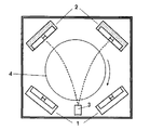
図1-8は各々四つのマグネトロンと回転可能な基板テーブル4とを有するPVDスパッタリング装置のコーテイング用チャンバを示す。マグネトロンは、遮蔽手段と冷却装置と磁石系とを備え、覆われた後部と、スパッタされる物質からなり覆われていないターゲットとで構成されている。図示の例では、それぞれのターゲットは、長方形の板として形成され、その前部は基板テーブル4に面している。 FIGS. 1-8 show the coating chambers of a PVD sputtering apparatus each having four magnetrons and a rotatable substrate table 4. The magnetron includes a shielding means, a cooling device, and a magnet system, and includes a covered rear portion and an uncovered target made of a material to be sputtered. In the example shown, each target is formed as a rectangular plate, with its front facing the substrate table 4.
図示の実施例において、少なくとも一つのマグネトロンは、各々の場合においてHPPMSマグネトロンとして形成されており、図面ではターゲットの上に”H”を付して識別されている。「HPPMSマグネトロン」の指定は、主としてその接続方式に関連している。すなわち、HPPMSマグネトロンはHPPMS電源に接続される一方、在来型のUBMマグネトロンは在来型の直流電源若しくは、従来エネルギーの電圧パルスを出力する従来のパルス電源に接続される。図示の例では、マグネトロン自体はみな構造、即ちターゲットの形状及び寸法、磁石系、冷却機構などが同じである。あるいは、例えば磁場の強度若しくは形状、冷却機構の規模に関し、各応用形態にしたがって、HPPMSマグネトロンや在来型のUBMマグネトロンなどのマグネトロンを適応化することも可能である。 In the illustrated embodiment, the at least one magnetron is in each case formed as an HPPMS magnetron, identified in the drawing with an “H” above the target. The designation of “HPPMS magnetron” is mainly related to the connection method. That is, the HPPMS magnetron is connected to an HPPMS power supply, while the conventional UBM magnetron is connected to a conventional DC power supply or a conventional pulse power supply that outputs a voltage pulse of conventional energy. In the illustrated example, the magnetrons themselves all have the same structure, that is, the shape and dimensions of the target, the magnet system, the cooling mechanism, and the like. Alternatively, for example, regarding the strength or shape of the magnetic field and the scale of the cooling mechanism, it is possible to adapt a magnetron such as an HPPMS magnetron or a conventional UBM magnetron according to each application form.
HPPMSマグネトロンのターゲットはそれぞれ、別個のHPPMS電源で駆動される。個々の実施例の各々に示すように、同電位にあるターゲットのシールディング及び/又はチャンバ壁、あるいは離れたアノードが、それぞれ陽極として機能する。HPPMSマグネトロンのターゲットは、スパッタリング動作において金属イオンを生成する。この金属イオンは、基板テーブルによって近くを移動する基板の前処理若しくはコーテイングに供される。離れたアノードの場合、コーテイングの間電源によってチャンバ壁に対し正の電位VCに保持される。 Each HPPPMS magnetron target is driven by a separate HPPMS power supply. As shown in each individual embodiment, target shielding and / or chamber walls at the same potential, or a separate anode, each function as an anode. The HPPPMS magnetron target generates metal ions in a sputtering operation. This metal ion is subjected to pretreatment or coating of the substrate moving nearby by the substrate table. In the case of a remote anode, it is held at a positive potential V C with respect to the chamber wall by the power supply during coating.
第1の実施例(図1)では、二つのHPPMSマグネトロン1と二つの在来型のUBMマグネトロン2が、約0.7m3の容積を有する金属コーティング用チャンバのチャンバ壁近傍に配置してある。これらの間に、回転する基板テーブル4がある。基板テーブル4は回転板3からなり、その上のラックに基板11が固定されているとともに、導電状態で接続されている。基板はコーティングの対象となる物体で、その形状は例えば工具のようにそれぞれの応用に対応した形状となっている。基板は、変化する距離関係で自転する回転板の上で、マグネトロンの前を移動していく。アノード3に対して基板バイアス電圧VBが基板に導電接続している基板テーブル4に印加される。
In the first embodiment (FIG. 1), two
在来型マグネトロン2がコーテイングの間アノードに対して駆動されるが、これらのマグネトロン2は基板テーブル4に対して互いに反対側に位置する。この目的で、マグネトロン2に応じた個々の電源ユニットが電圧VM1及びVM2を発生する。これらの電圧により、各マグネトロン2はカソードとして、アノード3に対し負の電位におかれる。マグネトロン2とアノード3との間の大きな距離により、陰極2及び空間で生成された電子は、チャンバを通って長い距離を移動し、更なるイオン化を生じさせる。このようにして、基板11を含む全コーテイング容積に対し高い気体イオン密度を供給できる。
HPPMSマグネトロン1のターゲットは、主として金属イオンを同時に供給する。本例では、これらはマグネトロンの接地された遮蔽手段に対して駆動される。前処理及びコーテイング処理の間、遮蔽手段は陽極の役割を果たす。純粋に在来型のマグネトロンの駆動に比較すると、HPPMSマグネトロン1の動作により、金属イオンの量が増加するので、実質的な膜品質及び密着性の改善をもたらす。
The
図2は、コーテイング装置のHPPMS電源14を示す模式図である。HPPMS電源14は、左下にあるHPPMSマグネトロン1用のものをただ例示的に示しており、他のHPPMSマグネトロンはさらに同一のHPPMS電源(図示せず)を備えている。HPPMS電源14は、スイッチング素子5と、容量素子6、と直流電源ユニット7とからなる。
FIG. 2 is a schematic diagram showing the
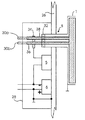
図9は、スイッチング素子5の模式図である。スイッチング素子5は、IGBTとして構成されたパワートランジスタからなり、容量素子6とHPPMSマグネトロン1との間に直列に配置している。IGBT16は制御ユニット20により駆動される。制御ユニット20はさらに駆動インターフェース24を含み、これによりスイッチング素子の状態が決められる。パルスの幅及びタイミングを規定する外部の制御コンピュータが、適切な態様で制御ユニット20を制御する。
FIG. 9 is a schematic diagram of the
容量素子6は容量バンク、即ち個々の容量の並列接続として提供されている。好適な例では、個々の容量は、各々2000Vを超える耐圧で用いられる。この好適な実施例では、必要な数だけ多くの個々の容量を並列接続して、容量バンク6の適切な総容量、例えば30μF又は50μFを達成している。
The
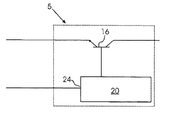
図2に示すように、最初の抽象的な表現では、スイッチング素子5と容量素子6は、チャンバ壁の外側で関連する電気−真空通路8にある陰極の直近にある。スイッチング素子の冷却は、チャンバ壁の冷却回路によって行われる。あるいは空冷も可能である。
As shown in FIG. 2, in the first abstract representation, the switching
パルスの休止期間中に容量バンク6の容量を充電するためのDC電源7は、パルス電力に対する要求に比べると、低い電力要求ですみ、離れたスイッチキャビネットに置かれている。
The DC power supply 7 for charging the capacity of the
図10において、チャンバ壁26に配置した容量バンク6とスイッチング素子5が、模式的に示されている。これらはハウジング28に配されており、チャンバ壁26に直接搭載されている。
In FIG. 10, the
チャンバに配されたHPPMSマグネトロン1のために、水冷機構が設けてあり、冷却媒体の入口30aと出口30bからなる。冷却媒体源は、最初ホースを介してハウジング28に供給される。続いて、チャンバ壁26の真空絶縁体32を挿通した銅管36,38により、HPPMSマグネトロン1に対する冷却媒体の供給及び排出を行う。
A water cooling mechanism is provided for the
銅管36,38は又スイッチング素子5からマグネトロン1に対してHPPMS電流パルスを導くための導電体として用いられる。この目的で、スイッチング素子5の電気出力はスリーブクランプ34により二つの管36,38に電気的に接続している。絶縁体32がチャンバ壁26に対する電気的な絶縁を提供している。
The
この結果、一方では真空通路8の構造が非常に単純になる。他方では、管36,38が非常に高い電流を導くために比較的大きな断面積を有する導体として優れて用いられる。管36,38自体が冷却媒体を導くため、追加の負荷なしに、導電体の冷却を行うことができる。
As a result, on the one hand, the structure of the
容量バンク6とスイッチング素子5はかくして互いにすぐ近くに配置できる。即ち、お互いから80cmより少ない距離に置かれ、好ましくは20cm未満におかれ、電流パルスをが流れる導体の距離を可能な限り短く保持できる。容量バンク6とスイッチング素子5は又、チャンバ壁26の反対側に配置されたHPPMSマグネトロン1の近傍に搭載できるので、これによっても電流路を短く保つことができ、好ましくはスイッチング素子5からHPPMSマグネトロン1まで50cm未満、特に好ましくは30cm未満に保持できる。
The
さらには、配置をこのように構成することで、HPPMSパルスの電流をを導く導体を最小の長さで真空チャンバの外側に配置することができる。金属の真空チャンバは、ファラディ遮蔽として働くので、設備の外側に対する電磁的な干渉を最小限にでき、又高い動作安全性を達成できる。 Furthermore, by arranging the arrangement in this way, the conductor for guiding the current of the HPPMS pulse can be arranged outside the vacuum chamber with a minimum length. The metal vacuum chamber acts as a Faraday shield so that electromagnetic interference to the outside of the facility can be minimized and high operational safety can be achieved.
第1の実施形態のコーテイング装置の例示的な構成では、チタンだけからなる第1のHPPMSターゲットを除く総てのターゲットがアルミニウムを挿入して組み込んだチタン板(Ti−Alターゲット)からなる。 In the exemplary configuration of the coating apparatus according to the first embodiment, all targets except for the first HPPMS target made of only titanium are made of a titanium plate (Ti-Al target) into which aluminum is inserted and incorporated.
第1の実施形態によるコーテイング装置の動作を以下に説明する。これは、基板テーブル4に配された工具などの物体(基板)11を前処理し且つコーテイングする例示形態である。 The operation of the coating apparatus according to the first embodiment will be described below. This is an exemplary form in which an object (substrate) 11 such as a tool disposed on the substrate table 4 is preprocessed and coated.
基板はまず約500℃まで加熱される。第1のエッチング工程で、アルゴンガスがチャンバに導入され、且つ在来型の二つのマグネトロン2がスイッチングの間、陰極として動作する電極3に対して約45cmの距離で、各マグネトロン2は共通に陽極として動作する。ここで、基板は負の電位に維持される。このようにして基板の近傍に生成された高密度の気体イオンは、第1のエッチング工程で初期的な清浄化と基板表面の活性化をもたらす。
The substrate is first heated to about 500 ° C. In the first etching step, argon gas is introduced into the chamber and the conventional two
第2の工程で、第1のエッチング工程と動作を同じにしたうえで、さらにターゲットがチタンのみからなる第1のHPPMSマグネトロン1を低いアルゴン圧で駆動する。電圧VB及びVCを適切に調節して、チャンバ壁を基準にして−1100vのより高い新しい負電位を基板に印加する。金属イオンが基板表面を清浄にし且つエッチングする。小さい比率でイオンが基板表面近傍に打ち込まれる。前と同様にアルゴン圧が依然としてあるので、アルゴンイオンによる照射も同時に起きている。
In the second step, the same operation as that of the first etching step is performed, and the
数分間、例えば一例で5分間の遷移期間の間に、基板バイアスは連続的に−1100Vから−100Vまで(絶対値で)減少する。これにより、薄いTiの界面が得られる。 During a transition period of several minutes, for example 5 minutes in the example, the substrate bias continuously decreases (in absolute value) from -1100V to -100V. Thereby, a thin Ti interface is obtained.
続いて、数分の間窒素が導入される。TiNからなる薄い硬質金属層が形成される。続いて、アルゴンガス及び反応ガスの流量を増やし、且つ(Ti−Alターゲットを備えた)第2のHPPMSマグネトロンが追加的に駆動される。さらに、在来型のマグネトロン2がこの時陽極として働く電極3に対して陰極として直流駆動される。
Subsequently, nitrogen is introduced for several minutes. A thin hard metal layer made of TiN is formed. Subsequently, the flow rates of argon gas and reaction gas are increased, and the second HPPMS magnetron (with Ti-Al target) is additionally driven. Further, the
三つの追加したマグネトロンは、Al及びTiイオンに加えて、Al及びTi原子を放出する。個々のマグネトロンの出力を調整することで、硬質層の化学量論的な組成を調整する。 Three additional magnetrons emit Al and Ti atoms in addition to Al and Ti ions. By adjusting the output of individual magnetrons, the stoichiometric composition of the hard layer is adjusted.
マグネトロン2の正面で生成された電子は、電場の中で陽極3に向かって移動し、かくして更なる荷電粒子を基板の近傍で生成する。この電場は、図1及び後続する図面では、破線で象徴的に示されている。この線は、大略電極対を構成する二つの電極の間に進入する電界線に対応している。チャンバ内の他の電極は、この電場ラインのゆがみをもたらしている。
The electrons generated in front of the
基板が回転するため特に、経時的にかなりの変動が生じうる。しかし経時的な平均でとると、電場ラインは大略図示の軌跡となる。能動電極表面間の視線は、長い距離にわたって電場ラインからほとんどずれることが無い。回転する基板は、少なくとも部分的且つ一時的にこれらの視線を横切る。かくして生成された気体イオンは、高い密度を伴って基板の上で利用可能になる。イオンは、コーテイング処理の間基板バイアス電圧VBによって、基板に向かって加速される。スパッタガスのイオンは、かくして層を緻密化する一方、反応ガスのイオンはスパッタされた金属イオンや原子と反応して所望のコーテイング物質TiAlNをもたらす。金属原子は、主として在来型のUBMマグネトロンから発する一方、金属イオンは主としてHPPMSマグネトロンからもたらされる。この組み合わせにより、特に硬く密着性の層が良好な層形成速度で得られる。 In particular, considerable fluctuations can occur over time due to the rotation of the substrate. However, taking an average over time, the electric field line generally has a locus shown in the drawing. The line of sight between the active electrode surfaces hardly deviates from the electric field line over a long distance. The rotating substrate at least partially and temporarily crosses these lines of sight. The gas ions thus produced are available on the substrate with a high density. Ions are accelerated toward the substrate by the substrate bias voltage V B during the coating process. Sputtering gas ions thus densify the layer, while reactive gas ions react with the sputtered metal ions and atoms to yield the desired coating material TiAlN. Metal atoms originate mainly from conventional UBM magnetrons, while metal ions come mainly from HPPMS magnetrons. With this combination, a particularly hard and adhesive layer can be obtained at a good layer formation rate.
一方もし、層が同じ実験構成でただ在来型のUBMマグネトロンのみを使って生成した場合、結果はより低い高度と密着性で且つ高い粗度の層になる。 On the other hand, if the layer was produced in the same experimental configuration using only a conventional UBM magnetron, the result would be a lower altitude and adhesion and higher roughness layer.
X38CrMoV51の鋼鉄板を処理すると、1400MPaまで硬くなり、半径10mmのミルの工具寿命を21%程度伸ばせる。 When a steel plate of X38CrMoV51 is processed, it hardens to 1400 MPa, and the tool life of a 10 mm radius mill can be extended by about 21%.
比較例では、HPPMSマグネトロンがUBMマグネトロンとともに使われたが、全てのマグネトロンが接地された遮蔽に対して駆動された。この比較例では、在来型のUBMマグネトロンのみで得られたコーテイングに比べると、部分的に密着性及び硬度が改善している一方、基板全体にわたって層特性は均一にならなかった。 In the comparative example, an HPPMS magnetron was used with a UBM magnetron, but all magnetrons were driven to grounded shielding. In this comparative example, the adhesion and hardness were partially improved as compared with the coating obtained with the conventional UBM magnetron alone, but the layer characteristics were not uniform over the entire substrate.
図3の第2実施形態は、四つのHPPMSマグネトロンを設けた他は、第1実施形態と同じである。二つのHPPMSマグネトロンは、離れた陽極に対して駆動され、その結果電子は長い距離を移動し、コーテイング容積全体で、高い気体イオン化をもたらす。 The second embodiment of FIG. 3 is the same as the first embodiment except that four HPPMS magnetrons are provided. The two HPPMS magnetrons are driven against a distant anode so that the electrons travel a long distance resulting in high gas ionization throughout the coating volume.
図4は、図3を参照しつつ、第2の実施形態におけるHPPMSマグネトロンと対応する対向電極との接続の例示態様を示す。基板テーブルの反対側にある陽極3用の電気配線9は、遮蔽シート(図示せず)の背後にあるチャンバ壁に沿って真空チャンバの内側に延設されている。この構成により、コーテイング装置の外側からの電磁干渉を最小にし、高い動作安全性が得られる。
FIG. 4 shows an exemplary mode of connection between the HPPMS magnetron and the corresponding counter electrode in the second embodiment with reference to FIG. The
第2実施形態による配置で基板のコーテイング処理の間、より大きな硬度と一方では高い張力とを備えた層が生成された他、同じ構成と同じ処理工程が行われた。これらの層は、特に超硬加工に有利であり、好ましくは小さな層厚に限って適用される。第1実施形態の応用例に比べると、工具寿命はさらに16%延びており、換言すると従来のコーテイングに比べてトータルで37%の改善になっている。 During the coating process of the substrate with the arrangement according to the second embodiment, a layer with greater hardness and on the other hand higher tension was generated, and the same processing steps with the same configuration were performed. These layers are particularly advantageous for carbide processing and are preferably applied only to small layer thicknesses. Compared to the application example of the first embodiment, the tool life is further extended by 16%, in other words, a total improvement of 37% compared to the conventional coating.
図5は、コーテイング装置の第3実施形態を示しており、好ましくは、基板の前処理及び/又は例えば酸化アルミニウムなど酸化層などの非導体層による基板のコーテイングに用いられる。コーテイング装置は、以下に述べる接続関係を除いて、上述した実施形態と同じであり、二つのHPPMSマグネトロンと二つの在来型マグネトロンとからなる。HPPMSマグネトロンの一つは、クロムのターゲットを装着しており、前処理と中間層の形成のみに使われる。他のマグネトロンのターゲットはアルミニウムからなる。二つの在来型のUBMマグネトロンは、コーテイングのために二重マグネトロンモードで動作する。 FIG. 5 shows a third embodiment of the coating apparatus, which is preferably used for substrate pretreatment and / or substrate coating with a non-conductive layer such as an oxide layer such as aluminum oxide. The coating apparatus is the same as that of the above-described embodiment except for the connection relationship described below, and includes two HPPMS magnetrons and two conventional magnetrons. One of the HPPPMS magnetrons is equipped with a chrome target and is used only for pretreatment and intermediate layer formation. Other magnetron targets are made of aluminum. Two conventional UBM magnetrons operate in a dual magnetron mode for coating.
酸化層を生成するための例示態様として、以下に第3実施形態にかかるコーテイング装置の動作を説明する。 As an exemplary mode for generating the oxide layer, the operation of the coating apparatus according to the third embodiment will be described below.
まず、第1実施形態の例示態様動作に類似したエッチング処理が行われる。ただしここでは、HPPMSチタンターゲットの代わりにHPPMSクロムターゲットが用いられる。第1の例と同じく、最初にターゲット物質の金属層を堆積し、続いて反応ガスを導入することにより、硬質物質の中間層を生成する。第3実施形態の例示動作では、最初にクロム層を堆積し、続いて反応ガスとして窒素を導入することで、CrN硬質物質の中間層を生成する。 First, an etching process similar to the exemplary operation of the first embodiment is performed. However, here, an HPPMS chromium target is used instead of the HPPMS titanium target. As in the first example, an intermediate layer of hard material is generated by first depositing a metal layer of target material and subsequently introducing a reactive gas. In the exemplary operation of the third embodiment, an intermediate layer of CrN hard material is generated by first depositing a chromium layer and subsequently introducing nitrogen as a reactive gas.
更なるコーテイング動作で、窒素の反応ガスを酸素で置き換えて、まず非常に薄いCr−N−O遷移層を形成し、ついでCr2O3の硬質物質中間層を形成する。 In a further coating operation, the nitrogen reactive gas is replaced with oxygen to form a very thin Cr—N—O transition layer first, followed by a Cr 2 O 3 hard material intermediate layer.
続いてCrマグネトロンの電力を下げる一方、AlHPPMSマグネトロン及び二つの在来型Alマグネトロンに傾斜的に増大する電力を供給して、実際のAl2O3硬質物質層を生成する。 Subsequently, the power of the Cr magnetron is reduced, while increasing power is supplied to the AlHPPMS magnetron and the two conventional Al magnetrons to produce an actual Al 2 O 3 hard material layer.
ここで、AlHPPMSマグネトロンはチャンバ壁に対して駆動される。二つの在来型マグネトロンは45cmの距離で50kHzの二重マグネトロンモードにより駆動される。 Here, the AlHPPMS magnetron is driven against the chamber wall. The two conventional magnetrons are driven by a 50 kHz double magnetron mode at a distance of 45 cm.
Alターゲットを装着した二つの在来型マグネトロンとともにHPPMSマグネトロンを用いることで、高い層品質を達成できる。さらに、処理の安定性及び層の均一性が非常に良好で、荷電やアークもまれであることが示された。 High layer quality can be achieved by using an HPPMS magnetron with two conventional magnetrons fitted with an Al target. In addition, the processing stability and layer uniformity were very good, and charging and arcing were rare.
図6は、コーテイング装置の第4実施形態を示す。第4実施形態は、コーテイング装置が二つのHPPMSマグネトロンと二つの在来型マグネトロンを含み、これらが全て共通の陽極に接続して、全コーテイング容積で金属及び気体のイオンの高密度化を達成する他は、上述した実施形態と同じである。 FIG. 6 shows a fourth embodiment of the coating apparatus. In the fourth embodiment, the coating apparatus includes two HPPMS magnetrons and two conventional magnetrons, all connected to a common anode to achieve high density of metal and gas ions in the entire coating volume. Others are the same as the embodiment described above.
図7は、コーテイング装置の第5実施形態を示す。第5実施形態は、コーテイング装置が四つのHPPMSマグネトロンを含み、これらが全て共通の陽極に接続して、全コーテイング容積で金属イオンの高密度化を達成する他は、上述した実施形態と同じである。 FIG. 7 shows a fifth embodiment of the coating apparatus. The fifth embodiment is the same as the above-described embodiment except that the coating apparatus includes four HPPMS magnetrons, all connected to a common anode to achieve metal ion densification in the entire coating volume. is there.
第5実施形態にかかるコーテイング装置の動作では、金属イオンで事前にエッチングすることで、特に接着性に優れた層が得られる。層品質もまた大変良好である。さらに、高い均一性を有する層厚を凹形状で実現できる。ただし、他の例と比較すると、層形成速度はある程減じる。HPPMSマグネトロンに対する電源供給は先の例と同様に構成される。 In the operation of the coating apparatus according to the fifth embodiment, a layer having particularly excellent adhesion can be obtained by etching in advance with metal ions. The layer quality is also very good. Furthermore, the layer thickness having high uniformity can be realized in a concave shape. However, as compared with other examples, the layer formation rate decreases to some extent. The power supply to the HPPMS magnetron is configured in the same way as in the previous example.
さらに、図8に示すコーテイング装置の第6実施形態では、二つのHPPMSマグネトロンが互いに二極モードでパルス駆動されるほか、上述した実施形態と同じである。 Further, the sixth embodiment of the coating apparatus shown in FIG. 8 is the same as the above-described embodiment except that two HPPMS magnetrons are pulse-driven with each other in a bipolar mode.
第6実施形態では、二つのHPPMSマグネトロンが共通のHPPMS電源40に接続されている。電源40は、二つの電源ユニット7,7aからなり、これらは中央のタップ42に対して対称的に接続している。DC電源供給ユニット7,7aと平行に、容量素子6,6aが接続しており、これらは好ましくは第1実施形態を参照して説明したように両方とも容量バンクとして構成されている。各容量素子6,6aの各負極は、直列接続したスイッチング素子5,5aを介して、各マグネトロン1,1aのターゲットに接続している。
In the sixth embodiment, two HPPMS magnetrons are connected to a common
HPPMS電源40の二つの対称的な部分の各々は、制御ユニット12によって制御される二つの追加的なスイッチ10,10aによって短絡される。各々のターゲットが陽極と陰極との間で交代するマグネトロン1,1aの二極パルス駆動において、スイッチ10,10aは次のパルスで陽極となるべき各ターゲットを、対応するHPPMS電源の正極に接続する。他のスイッチは、開いた状態に置かれる。かくして各パルスごとに、二つのHPPMSマグネトロンの一方が陽極として動作し、他方が対応する陰極として動作する。
Each of the two symmetrical portions of the
スイッチ10,10aは電流が流れている間ではなく、パルスとパルスとの間で切り替えられるので、スイッチ10,10aに求められる条件はむしろ穏やかである。制御ユニット12は、スイッチ素子5,5a,10,10aを同期化するために設けてある。先と同様、スイッチング素子は共通にチャンバ背後壁に搭載され、共通の真空通路8を介してチャンバに挿通している電気配線により、HPPMSマグネトロンに接続している。可能な限り、電気配線はチャンバの内部に延設されており、好ましくはHPPMSパルスを導く全線船のうち、大部分がチャンバの内部にある。
Since the
代替の実施形態(図示せず)では、充電装置が配されており、パルスとパルスとの間で両方の容量バンク6,6aを充電するように構成されている。
In an alternative embodiment (not shown), a charging device is arranged and configured to charge both
図8に示した実施例の配置に拠れば、動作中充電が少なくなり、層は平滑になる。他の二つのマグネトロンもHPPMSマグネトロンでよく、同様に駆動される。これらを接地もしくは共通の対向電極3に対して駆動することも可能である。あるいは他の二つのマグネトロンは在来型のマグネトロンであってもよい。これらは例えば二重マグネトロンモードで若しくは接地及び共通電極に対して駆動することができる。
According to the arrangement of the embodiment shown in FIG. 8, there is less charge during operation and the layer is smooth. The other two magnetrons can also be HPPPMS magnetrons and are driven in the same way. It is also possible to drive them with respect to the ground or
Claims (14)
金属製のチャンバ壁(26)と、スパッタターゲットを有するマグネトロン(1,2)とを備えた真空チャンバからなり、
少なくとも一つのマグネトロンは、高電力パルスのマグネトロンスパッタリングプロセスで動作するHPPMSマグネトロン(1)として配されており、
スイッチング素子(5)を介して該HPPMSマグネトロン(1)のスパッタターゲットに容量素子(6)を接続することによって、電気パルスが該HPPMSマグネトロンに供給されている装置において、
該容量素子(6)は、並列接続したキャパシタからなる容量バンクとして構成され、
該スイッチング素子(5)と該容量素子(6)は、該チャンバ壁(26)の上に配されていることを特徴とする装置。 An apparatus for pre-processing and coating an object by magnetron sputtering,
A vacuum chamber comprising a metal chamber wall (26) and a magnetron (1, 2) having a sputter target;
At least one magnetron is arranged as an HPPPMS magnetron (1) operating in a high power pulsed magnetron sputtering process;
In an apparatus in which an electrical pulse is supplied to the HPPPMS magnetron by connecting a capacitive element (6) to the sputter target of the HPPPMS magnetron (1) via a switching element (5) ,
The capacitor (6) is configured as a capacitor bank composed of capacitors connected in parallel,
The device characterized in that the switching element (5) and the capacitive element (6) are arranged on the chamber wall (26) .
該容量素子(6)、該スイッチング素子(5)及び該真空通路(8)はユニットを形成している
請求項1に記載の装置。 A vacuum passage (8) is disposed in the chamber wall (26) for powering the HPPPMS magnetron,
The capacitive element (6), the switching element (5) and the vacuum passage (8) form a unit.
The apparatus of claim 1 .
冷却媒体が導管(36,38)を通って該HPPMSマグネトロン(1)に流入し、
該導管(36,38)は、真空通路(8)を介して該チャンバ壁(26)を貫通しており、
該導管(36,38)が導電体として用いられ、該導電体により電流が該スイッチング素子(5)から該HPPMSマグネトロン(1)に導かれている
請求項1又は2に記載の装置。 A cooling means is provided for the HPPPMS magnetron;
A cooling medium flows into the HPPPMS magnetron (1) through a conduit (36, 38);
The conduit (36, 38) passes through the chamber wall (26) via a vacuum passage (8);
The conduit (36, 38) is used as a conductor, and current is conducted from the switching element (5) to the HPPMS magnetron (1) by the conductor.
The apparatus according to claim 1 or 2 .
該冷却手段が該スイッチング素子の冷却にも用いられる
請求項1,2又は3に記載の装置。 A cooling means is provided for the chamber wall and / or a vacuum passage attached to the chamber wall;
The cooling means is also used for cooling the switching element.
The apparatus according to claim 1, 2 or 3 .
電気配線が該電極対の各電極のために配されており、
該電極対の二つの電極のための該電気配線は、共通の真空通路(8)若しくは二つの隣接する真空通路を介して、コーテイング用の該チャンバに挿通しており、該電気配線は、該チャンバの内部で該電極に延びている
請求項1,2,3又は4に記載の装置。 At least one electrode pair is disposed, at least one of the electrode pairs being an HPPPMS magnetron (1);
Electrical wiring is provided for each electrode of the electrode pair;
The electrical wiring for the two electrodes of the electrode pair passes through the common vacuum passage (8) or two adjacent vacuum passages into the coating chamber, the electrical wiring being Extends to the electrode inside the chamber
Apparatus according to claim 1, 2, 3 or 4 .
第1電極(1)及び第2電極(3)とを備えた少なくとも一つのプラズマ発生電極対を含み、
前記HPPMSマグネトロン(1)は該第1電極(1)であり、高電力パルスを用いたマグネトロンスパッタリングモードで動作し、
HPPMS電源が該第1電極と該第2電極との間に配されており、
該基板テーブル(4)に支持された物体が該電極対の能動面の間に位置するか、あるいは該電極対の能動面の間の空間を移動するように、該第1電極と該第2電極とを配置するようにした
請求項1,2,3,4又は5に記載の装置。 A substrate table (4) for supporting the object to be coated;
Comprising at least one plasma generating electrode pair comprising a first electrode (1) and a second electrode (3);
The HPPPMS magnetron (1) is the first electrode (1) and operates in a magnetron sputtering mode using a high power pulse;
An HPPPMS power source is disposed between the first electrode and the second electrode;
The first electrode and the second electrode are arranged such that an object supported on the substrate table (4) is located between the active surfaces of the electrode pair or moves in a space between the active surfaces of the electrode pair. The electrode was arranged
Apparatus according to claim 1, 2, 3, 4 or 5 .
請求項6に記載の装置。 At least one other electrode pair is arranged in the vacuum chamber, and at least one of the electrodes of the electrode pair is configured as a magnetron (2), which is connected to a DC power source or a conventional pulse power source The device according to claim 6 .
請求項6又は7に記載の装置。 The distance between the active surfaces of the at least one electrode pair is greater than 20 cm ;
Apparatus according to claim 6 or 7 .
バイアス電圧を発生するために、バイアス電圧源(VB)が該陽極(3)と該基板テーブル(4)との間に配されている、
請求項6,7又は8に記載の装置。 The second electrode is the anode (3);
In order to generate a bias voltage, a bias voltage source (V B ) is arranged between the anode (3) and the substrate table (4).
Apparatus according to claim 6, 7 or 8 .
請求項9に記載の装置。 The surface of the anode (3) exposed to the plasma during coating is smaller than the surface of the first electrode exposed to the plasma;
The apparatus according to claim 9 .
請求項9又は10に記載の装置。 A power supply (V C ) is disposed between the anode and the chamber wall and maintains the anode at a positive potential relative to the chamber wall during coating.
The apparatus according to claim 9 or 10 .
請求項9,10又は11に記載の装置。 12. A device according to claim 9, 10 or 11 , wherein during the coating at least two magnetrons are connected to a common anode (3).
該第1電極と該第2電極との間にHPPMS電力供給源(40)が配されており、
このHPPMS電力供給源により、該電極(1,1a)が相互にバイポーラ方式でパルス駆動される
請求項6に記載の装置。 The second electrode is an HPPPMS magnetron (1a);
An HPPPMS power supply source (40) is disposed between the first electrode and the second electrode,
7. The device according to claim 6 , wherein the electrodes (1, 1a) are pulsed with each other in a bipolar manner by the HPPPMS power supply.
該物体は、金属製のチャンバ壁(26)と、スパッタターゲットを有するマグネトロンとを有する真空チャンバに配され、
該真空チャンバの中でプラズマが発生し、該スパッタターゲットの少なくとも一つがスパッタされ、
該マグネトロンの少なくとも一つは、高電力パルスを用いたマグネトロンスパッタリングプロセスによりHPPMSマグネトロンとして動作し、
スイッチング素子(5)を介して容量素子(6)を該HPPSマグネトロン(1)の該スパッタターゲットに接続することにより、電気パルスを該HPPSマグネトロン(1)に供給する方法において、
該容量素子(6)は、並列接続したキャパシタからなる容量バンクとして構成され、
該スイッチング素子(5)と該容量素子(6)が、該チャンバ壁(26)の上に配されていることを特徴とする方法。 A method for pre-processing and coating an object by magnetron sputtering comprising:
The object is placed in a vacuum chamber having a metal chamber wall (26) and a magnetron with a sputter target;
Plasma is generated in the vacuum chamber and at least one of the sputter targets is sputtered;
At least one of the magnetrons operates as an HPPPMS magnetron by a magnetron sputtering process using high power pulses,
In a method of supplying an electric pulse to the HPPS magnetron (1) by connecting a capacitive element (6) to the sputter target of the HPPS magnetron (1) via a switching element (5),
The capacitor (6) is configured as a capacitor bank composed of capacitors connected in parallel,
Method according to claim 1, characterized in that the switching element (5) and the capacitive element (6) are arranged on the chamber wall (26).
Applications Claiming Priority (3)
| Application Number | Priority Date | Filing Date | Title |
|---|---|---|---|
| DE102008021128 | 2008-04-28 | ||
| DE102008021128.1 | 2008-04-28 | ||
| PCT/EP2009/003082 WO2009132822A2 (en) | 2008-04-28 | 2009-04-28 | Device and method for pretreating and coating bodies |
Publications (3)
| Publication Number | Publication Date |
|---|---|
| JP2011518950A JP2011518950A (en) | 2011-06-30 |
| JP2011518950A5 JP2011518950A5 (en) | 2012-06-07 |
| JP5448232B2 true JP5448232B2 (en) | 2014-03-19 |
Family
ID=40885977
Family Applications (1)
| Application Number | Title | Priority Date | Filing Date |
|---|---|---|---|
| JP2011505437A Active JP5448232B2 (en) | 2008-04-28 | 2009-04-28 | Apparatus and method for pre-processing and coating an object |
Country Status (6)
| Country | Link |
|---|---|
| US (1) | US9812299B2 (en) |
| EP (1) | EP2272080B1 (en) |
| JP (1) | JP5448232B2 (en) |
| CN (1) | CN102027564B (en) |
| DE (1) | DE202009018428U1 (en) |
| WO (1) | WO2009132822A2 (en) |
Families Citing this family (29)
| Publication number | Priority date | Publication date | Assignee | Title |
|---|---|---|---|---|
| DE102008050499B4 (en) | 2008-10-07 | 2014-02-06 | Systec System- Und Anlagentechnik Gmbh & Co. Kg | PVD coating method, apparatus for carrying out the method and substrates coated by the method |
| DE202010001497U1 (en) * | 2010-01-29 | 2010-04-22 | Hauzer Techno-Coating B.V. | Coating device with a HIPIMS power source |
| JP5765627B2 (en) * | 2010-09-27 | 2015-08-19 | 日立金属株式会社 | Coated tool having excellent durability and method for producing the same |
| SG194568A1 (en) | 2011-04-20 | 2013-12-30 | Oerlikon Trading Ag | Method for supplying sequential power impulses |
| DE102011117177A1 (en) * | 2011-10-28 | 2013-05-02 | Oerlikon Trading Ag, Trübbach | Method for providing sequential power pulses |
| BRPI1102335A2 (en) | 2011-05-27 | 2013-06-25 | Mahle Metal Leve Sa | element provided with at least one sliding surface with a coating for use on an internal combustion engine or compressor |
| US9416440B2 (en) | 2011-09-30 | 2016-08-16 | Cemecon Ag | Coating of substrates using HIPIMS |
| DE102011117994A1 (en) * | 2011-11-09 | 2013-05-16 | Oerlikon Trading Ag, Trübbach | HIPIMS layers |
| JP5344204B2 (en) * | 2012-03-05 | 2013-11-20 | 三菱マテリアル株式会社 | Surface coated cutting tool |
| US9264150B2 (en) * | 2012-03-28 | 2016-02-16 | Globalfoundries Inc. | Reactive metal optical security device and methods of fabrication and use |
| DE102012013577A1 (en) | 2012-07-10 | 2014-01-16 | Oerlikon Trading Ag, Trübbach | Pulsed Power coating method |
| US9126273B2 (en) | 2012-12-17 | 2015-09-08 | Kennametal Inc | Tool for the cutting machining of workpieces and process for coating substrate bodies |
| EP2784799B1 (en) | 2013-03-28 | 2022-12-21 | CemeCon AG | Dense, hard coatings on substrates using HIPIMS |
| DE102013106351A1 (en) * | 2013-06-18 | 2014-12-18 | Innovative Ion Coatings Ltd. | Process for the pretreatment of a surface to be coated |
| US9677168B2 (en) | 2013-10-08 | 2017-06-13 | TPK America, LLC | Touch panel and method for manufacturing the same |
| US20150354054A1 (en) * | 2014-06-06 | 2015-12-10 | Applied Materials, Inc. | Cooled process tool adapter for use in substrate processing chambers |
| FR3025929B1 (en) * | 2014-09-17 | 2016-10-21 | Commissariat Energie Atomique | NUCLEAR FUEL TANKS, METHODS OF MANUFACTURE AND USE AGAINST OXIDATION. |
| DE102014115492A1 (en) | 2014-10-24 | 2016-04-28 | Cemecon Ag | Method and device for generating an electronic discharge |
| US9812305B2 (en) * | 2015-04-27 | 2017-11-07 | Advanced Energy Industries, Inc. | Rate enhanced pulsed DC sputtering system |
| US20180334739A1 (en) * | 2015-11-10 | 2018-11-22 | Sandvik Intellectual Property Ab | Method for pre-treating a surface for coating |
| SG11201803970RA (en) | 2015-11-12 | 2018-06-28 | Oerlikon Surface Solutions Ag Pfaeffikon | Sputtering arrangement and sputtering method for optimized distribution of the energy flow |
| US10612132B2 (en) | 2015-11-27 | 2020-04-07 | Cemecon Ag | Coating a body with a diamond layer and a hard material layer |
| US20180108519A1 (en) * | 2016-10-17 | 2018-04-19 | Applied Materials, Inc. | POWER DELIVERY FOR HIGH POWER IMPULSE MAGNETRON SPUTTERING (HiPIMS) |
| KR101885123B1 (en) * | 2017-03-31 | 2018-08-03 | 한국알박(주) | Magnet control system of magnetron sputtering apparatus |
| CN109112496B (en) * | 2018-09-26 | 2020-11-24 | 武汉华星光电半导体显示技术有限公司 | Magnetron sputtering equipment and method for removing oxide layer on substrate |
| DE102019124616A1 (en) * | 2019-09-12 | 2021-03-18 | Cemecon Ag | Multi-layer coating |
| FI3960896T3 (en) * | 2020-04-20 | 2024-02-20 | Joint Stock Company Tvel | Method of ion-plasma application of corrosion-resistant film coatings on articles made from zirconium alloys |
| CN112708854A (en) * | 2020-12-19 | 2021-04-27 | 合肥开泰机电科技有限公司 | Vacuum coating structure for large-area brazing |
| WO2023099757A1 (en) * | 2021-12-03 | 2023-06-08 | Université De Namur | A process for depositing a coating on a substrate by means of pvd methods and the coating obtained by said process |
Family Cites Families (21)
| Publication number | Priority date | Publication date | Assignee | Title |
|---|---|---|---|---|
| US3635811A (en) * | 1967-11-06 | 1972-01-18 | Warner Lambert Co | Method of applying a coating |
| US4098452A (en) * | 1975-03-31 | 1978-07-04 | General Electric Company | Lead bonding method |
| US5096562A (en) * | 1989-11-08 | 1992-03-17 | The Boc Group, Inc. | Rotating cylindrical magnetron structure for large area coating |
| US5962923A (en) * | 1995-08-07 | 1999-10-05 | Applied Materials, Inc. | Semiconductor device having a low thermal budget metal filling and planarization of contacts, vias and trenches |
| GB9705022D0 (en) | 1997-03-11 | 1997-04-30 | James Alec C | Support means locatable so as to span a gap between two surfaces |
| SE9704607D0 (en) | 1997-12-09 | 1997-12-09 | Chemfilt R & D Ab | A method and apparatus for magnetically enhanced sputtering |
| DK0975818T3 (en) * | 1997-04-14 | 2003-01-06 | Cemecon Ceramic Metal Coatings | Method and apparatus for PVD coating |
| US20020046944A1 (en) * | 2000-06-28 | 2002-04-25 | Ehood Geva | Method and apparatus for reducing noise in a sputtering chamber |
| SE525231C2 (en) | 2001-06-14 | 2005-01-11 | Chemfilt R & D Ab | Method and apparatus for generating plasma |
| JP4101554B2 (en) * | 2001-08-17 | 2008-06-18 | 株式会社神戸製鋼所 | Sputtering apparatus and method |
| US7172681B2 (en) * | 2003-02-05 | 2007-02-06 | Bridgestone Corporation | Process for producing rubber-based composite material |
| DE10318364A1 (en) * | 2003-04-23 | 2004-11-18 | Fraunhofer-Gesellschaft zur Förderung der angewandten Forschung e.V. | Device for coating a stationary substrate by pulse magnetron sputtering |
| US7663319B2 (en) * | 2004-02-22 | 2010-02-16 | Zond, Inc. | Methods and apparatus for generating strongly-ionized plasmas with ionizational instabilities |
| EP1609882A1 (en) * | 2004-06-24 | 2005-12-28 | METAPLAS IONON Oberflächenveredelungstechnik GmbH | Coating device and method by cathodic sputtering |
| SE0402644D0 (en) | 2004-11-02 | 2004-11-02 | Biocell Ab | Method and apparatus for producing electric discharges |
| JP2006161088A (en) * | 2004-12-06 | 2006-06-22 | Canon Inc | Sputtering apparatus |
| US20060260938A1 (en) * | 2005-05-20 | 2006-11-23 | Petrach Philip M | Module for Coating System and Associated Technology |
| DE102005033769B4 (en) * | 2005-07-15 | 2009-10-22 | Systec System- Und Anlagentechnik Gmbh & Co.Kg | Method and apparatus for multi-cathode PVD coating and substrate with PVD coating |
| DE102006017382A1 (en) * | 2005-11-14 | 2007-05-16 | Itg Induktionsanlagen Gmbh | Method and device for coating and / or treating surfaces |
| GB0608582D0 (en) * | 2006-05-02 | 2006-06-07 | Univ Sheffield Hallam | High power impulse magnetron sputtering vapour deposition |
| DE102006021994B4 (en) * | 2006-05-10 | 2017-08-03 | Cemecon Ag | coating process |
-
2009
- 2009-04-28 JP JP2011505437A patent/JP5448232B2/en active Active
- 2009-04-28 US US12/989,882 patent/US9812299B2/en active Active
- 2009-04-28 WO PCT/EP2009/003082 patent/WO2009132822A2/en active Application Filing
- 2009-04-28 EP EP09737866A patent/EP2272080B1/en active Active
- 2009-04-28 CN CN200980115777XA patent/CN102027564B/en active Active
- 2009-04-28 DE DE202009018428U patent/DE202009018428U1/en not_active Expired - Lifetime
Also Published As
| Publication number | Publication date |
|---|---|
| WO2009132822A3 (en) | 2010-01-21 |
| EP2272080A2 (en) | 2011-01-12 |
| EP2272080B1 (en) | 2012-08-01 |
| CN102027564A (en) | 2011-04-20 |
| US20110180389A1 (en) | 2011-07-28 |
| US9812299B2 (en) | 2017-11-07 |
| CN102027564B (en) | 2013-05-22 |
| DE202009018428U1 (en) | 2011-09-28 |
| WO2009132822A2 (en) | 2009-11-05 |
| JP2011518950A (en) | 2011-06-30 |
Similar Documents
| Publication | Publication Date | Title |
|---|---|---|
| JP5448232B2 (en) | Apparatus and method for pre-processing and coating an object | |
| US6413382B1 (en) | Pulsed sputtering with a small rotating magnetron | |
| JP4208970B2 (en) | Continuous deposition of insulating materials using multiple anodes with alternating positive and negative voltages | |
| EP2157205B1 (en) | A high-power pulsed magnetron sputtering process as well as a high-power electrical energy source | |
| JP2011518950A5 (en) | ||
| KR100260601B1 (en) | The substrate coating apparatus | |
| EP2597172B1 (en) | Ion bombardment apparatus and method for cleaning of surface of base material using the same | |
| JPH0841636A (en) | Method and apparatus for reactive sputtering | |
| CN101528369B (en) | Method and apparatus for manufacturing cleaned substrates or clean substrates which are further processed | |
| JPH09186150A (en) | Apparatus for coating substrate by chemical deposition | |
| US20080308410A1 (en) | Redundant Anode Sputtering Method and Assembly | |
| JP5232190B2 (en) | Source for vacuum processing process | |
| EP0818801A2 (en) | Plasma treating apparatus | |
| US20070144901A1 (en) | Pulsed cathodic arc plasma | |
| JP5649333B2 (en) | Ion bombardment apparatus and substrate surface cleaning method using the apparatus | |
| JP7026464B2 (en) | Method for depositing layers using magnetron sputtering equipment | |
| KR100480357B1 (en) | Film deposition apparatus having dual magnetron sputtering system and ion beam source which are synchronized | |
| EP2159820B1 (en) | A physical vapour deposition coating device as well as a physical vapour deposition method | |
| KR101478216B1 (en) | Ion Source and Ion Beam Processing Apparatus therewith | |
| JP6832572B2 (en) | Method of forming a decorative film by the magnetron sputtering method | |
| EP2607517A1 (en) | Low temperature arc ion plating coating | |
| RU2423754C2 (en) | Method and device to manufacture cleaned substrates or pure substrates exposed to additional treatment | |
| JP2004035935A (en) | Film deposition system and film deposition method |
Legal Events
| Date | Code | Title | Description |
|---|---|---|---|
| A521 | Request for written amendment filed |
Free format text: JAPANESE INTERMEDIATE CODE: A523 Effective date: 20120420 |
|
| A621 | Written request for application examination |
Free format text: JAPANESE INTERMEDIATE CODE: A621 Effective date: 20120420 |
|
| A977 | Report on retrieval |
Free format text: JAPANESE INTERMEDIATE CODE: A971007 Effective date: 20130704 |
|
| A131 | Notification of reasons for refusal |
Free format text: JAPANESE INTERMEDIATE CODE: A131 Effective date: 20130710 |
|
| A601 | Written request for extension of time |
Free format text: JAPANESE INTERMEDIATE CODE: A601 Effective date: 20130928 |
|
| A602 | Written permission of extension of time |
Free format text: JAPANESE INTERMEDIATE CODE: A602 Effective date: 20131007 |
|
| A521 | Request for written amendment filed |
Free format text: JAPANESE INTERMEDIATE CODE: A523 Effective date: 20131107 |
|
| TRDD | Decision of grant or rejection written | ||
| A01 | Written decision to grant a patent or to grant a registration (utility model) |
Free format text: JAPANESE INTERMEDIATE CODE: A01 Effective date: 20131203 |
|
| A61 | First payment of annual fees (during grant procedure) |
Free format text: JAPANESE INTERMEDIATE CODE: A61 Effective date: 20131221 |
|
| R150 | Certificate of patent or registration of utility model |
Ref document number: 5448232 Country of ref document: JP Free format text: JAPANESE INTERMEDIATE CODE: R150 Free format text: JAPANESE INTERMEDIATE CODE: R150 |
|
| R250 | Receipt of annual fees |
Free format text: JAPANESE INTERMEDIATE CODE: R250 |
|
| R250 | Receipt of annual fees |
Free format text: JAPANESE INTERMEDIATE CODE: R250 |
|
| R250 | Receipt of annual fees |
Free format text: JAPANESE INTERMEDIATE CODE: R250 |
|
| R250 | Receipt of annual fees |
Free format text: JAPANESE INTERMEDIATE CODE: R250 |
|
| R250 | Receipt of annual fees |
Free format text: JAPANESE INTERMEDIATE CODE: R250 |
|
| R250 | Receipt of annual fees |
Free format text: JAPANESE INTERMEDIATE CODE: R250 |
|
| R250 | Receipt of annual fees |
Free format text: JAPANESE INTERMEDIATE CODE: R250 |
|
| R250 | Receipt of annual fees |
Free format text: JAPANESE INTERMEDIATE CODE: R250 |