JP5448232B2 - 物体を前処理及びコーテイングするための装置及び方法 - Google Patents
物体を前処理及びコーテイングするための装置及び方法 Download PDFInfo
- Publication number
- JP5448232B2 JP5448232B2 JP2011505437A JP2011505437A JP5448232B2 JP 5448232 B2 JP5448232 B2 JP 5448232B2 JP 2011505437 A JP2011505437 A JP 2011505437A JP 2011505437 A JP2011505437 A JP 2011505437A JP 5448232 B2 JP5448232 B2 JP 5448232B2
- Authority
- JP
- Japan
- Prior art keywords
- magnetron
- electrode
- hpppms
- coating
- hppms
- Prior art date
- Legal status (The legal status is an assumption and is not a legal conclusion. Google has not performed a legal analysis and makes no representation as to the accuracy of the status listed.)
- Active
Links
Images


Classifications
-
- H—ELECTRICITY
- H01—ELECTRIC ELEMENTS
- H01J—ELECTRIC DISCHARGE TUBES OR DISCHARGE LAMPS
- H01J37/00—Discharge tubes with provision for introducing objects or material to be exposed to the discharge, e.g. for the purpose of examination or processing thereof
- H01J37/32—Gas-filled discharge tubes
- H01J37/34—Gas-filled discharge tubes operating with cathodic sputtering
- H01J37/3402—Gas-filled discharge tubes operating with cathodic sputtering using supplementary magnetic fields
- H01J37/3405—Magnetron sputtering
- H01J37/3408—Planar magnetron sputtering
-
- C—CHEMISTRY; METALLURGY
- C23—COATING METALLIC MATERIAL; COATING MATERIAL WITH METALLIC MATERIAL; CHEMICAL SURFACE TREATMENT; DIFFUSION TREATMENT OF METALLIC MATERIAL; COATING BY VACUUM EVAPORATION, BY SPUTTERING, BY ION IMPLANTATION OR BY CHEMICAL VAPOUR DEPOSITION, IN GENERAL; INHIBITING CORROSION OF METALLIC MATERIAL OR INCRUSTATION IN GENERAL
- C23C—COATING METALLIC MATERIAL; COATING MATERIAL WITH METALLIC MATERIAL; SURFACE TREATMENT OF METALLIC MATERIAL BY DIFFUSION INTO THE SURFACE, BY CHEMICAL CONVERSION OR SUBSTITUTION; COATING BY VACUUM EVAPORATION, BY SPUTTERING, BY ION IMPLANTATION OR BY CHEMICAL VAPOUR DEPOSITION, IN GENERAL
- C23C14/00—Coating by vacuum evaporation, by sputtering or by ion implantation of the coating forming material
- C23C14/06—Coating by vacuum evaporation, by sputtering or by ion implantation of the coating forming material characterised by the coating material
- C23C14/14—Metallic material, boron or silicon
-
- C—CHEMISTRY; METALLURGY
- C23—COATING METALLIC MATERIAL; COATING MATERIAL WITH METALLIC MATERIAL; CHEMICAL SURFACE TREATMENT; DIFFUSION TREATMENT OF METALLIC MATERIAL; COATING BY VACUUM EVAPORATION, BY SPUTTERING, BY ION IMPLANTATION OR BY CHEMICAL VAPOUR DEPOSITION, IN GENERAL; INHIBITING CORROSION OF METALLIC MATERIAL OR INCRUSTATION IN GENERAL
- C23C—COATING METALLIC MATERIAL; COATING MATERIAL WITH METALLIC MATERIAL; SURFACE TREATMENT OF METALLIC MATERIAL BY DIFFUSION INTO THE SURFACE, BY CHEMICAL CONVERSION OR SUBSTITUTION; COATING BY VACUUM EVAPORATION, BY SPUTTERING, BY ION IMPLANTATION OR BY CHEMICAL VAPOUR DEPOSITION, IN GENERAL
- C23C14/00—Coating by vacuum evaporation, by sputtering or by ion implantation of the coating forming material
- C23C14/22—Coating by vacuum evaporation, by sputtering or by ion implantation of the coating forming material characterised by the process of coating
- C23C14/34—Sputtering
- C23C14/3435—Applying energy to the substrate during sputtering
- C23C14/345—Applying energy to the substrate during sputtering using substrate bias
-
- C—CHEMISTRY; METALLURGY
- C23—COATING METALLIC MATERIAL; COATING MATERIAL WITH METALLIC MATERIAL; CHEMICAL SURFACE TREATMENT; DIFFUSION TREATMENT OF METALLIC MATERIAL; COATING BY VACUUM EVAPORATION, BY SPUTTERING, BY ION IMPLANTATION OR BY CHEMICAL VAPOUR DEPOSITION, IN GENERAL; INHIBITING CORROSION OF METALLIC MATERIAL OR INCRUSTATION IN GENERAL
- C23C—COATING METALLIC MATERIAL; COATING MATERIAL WITH METALLIC MATERIAL; SURFACE TREATMENT OF METALLIC MATERIAL BY DIFFUSION INTO THE SURFACE, BY CHEMICAL CONVERSION OR SUBSTITUTION; COATING BY VACUUM EVAPORATION, BY SPUTTERING, BY ION IMPLANTATION OR BY CHEMICAL VAPOUR DEPOSITION, IN GENERAL
- C23C14/00—Coating by vacuum evaporation, by sputtering or by ion implantation of the coating forming material
- C23C14/22—Coating by vacuum evaporation, by sputtering or by ion implantation of the coating forming material characterised by the process of coating
- C23C14/34—Sputtering
- C23C14/3485—Sputtering using pulsed power to the target
-
- C—CHEMISTRY; METALLURGY
- C23—COATING METALLIC MATERIAL; COATING MATERIAL WITH METALLIC MATERIAL; CHEMICAL SURFACE TREATMENT; DIFFUSION TREATMENT OF METALLIC MATERIAL; COATING BY VACUUM EVAPORATION, BY SPUTTERING, BY ION IMPLANTATION OR BY CHEMICAL VAPOUR DEPOSITION, IN GENERAL; INHIBITING CORROSION OF METALLIC MATERIAL OR INCRUSTATION IN GENERAL
- C23C—COATING METALLIC MATERIAL; COATING MATERIAL WITH METALLIC MATERIAL; SURFACE TREATMENT OF METALLIC MATERIAL BY DIFFUSION INTO THE SURFACE, BY CHEMICAL CONVERSION OR SUBSTITUTION; COATING BY VACUUM EVAPORATION, BY SPUTTERING, BY ION IMPLANTATION OR BY CHEMICAL VAPOUR DEPOSITION, IN GENERAL
- C23C14/00—Coating by vacuum evaporation, by sputtering or by ion implantation of the coating forming material
- C23C14/22—Coating by vacuum evaporation, by sputtering or by ion implantation of the coating forming material characterised by the process of coating
- C23C14/34—Sputtering
- C23C14/35—Sputtering by application of a magnetic field, e.g. magnetron sputtering
- C23C14/352—Sputtering by application of a magnetic field, e.g. magnetron sputtering using more than one target
-
- H—ELECTRICITY
- H01—ELECTRIC ELEMENTS
- H01J—ELECTRIC DISCHARGE TUBES OR DISCHARGE LAMPS
- H01J37/00—Discharge tubes with provision for introducing objects or material to be exposed to the discharge, e.g. for the purpose of examination or processing thereof
- H01J37/32—Gas-filled discharge tubes
- H01J37/34—Gas-filled discharge tubes operating with cathodic sputtering
- H01J37/3411—Constructional aspects of the reactor
- H01J37/3444—Associated circuits
-
- H—ELECTRICITY
- H01—ELECTRIC ELEMENTS
- H01J—ELECTRIC DISCHARGE TUBES OR DISCHARGE LAMPS
- H01J37/00—Discharge tubes with provision for introducing objects or material to be exposed to the discharge, e.g. for the purpose of examination or processing thereof
- H01J37/32—Gas-filled discharge tubes
- H01J37/34—Gas-filled discharge tubes operating with cathodic sputtering
- H01J37/3464—Operating strategies
- H01J37/3467—Pulsed operation, e.g. HIPIMS
-
- H—ELECTRICITY
- H01—ELECTRIC ELEMENTS
- H01J—ELECTRIC DISCHARGE TUBES OR DISCHARGE LAMPS
- H01J37/00—Discharge tubes with provision for introducing objects or material to be exposed to the discharge, e.g. for the purpose of examination or processing thereof
- H01J37/32—Gas-filled discharge tubes
- H01J37/34—Gas-filled discharge tubes operating with cathodic sputtering
- H01J37/3464—Operating strategies
- H01J37/3473—Composition uniformity or desired gradient
Landscapes
- Chemical & Material Sciences (AREA)
- Engineering & Computer Science (AREA)
- Physics & Mathematics (AREA)
- Plasma & Fusion (AREA)
- Analytical Chemistry (AREA)
- Chemical Kinetics & Catalysis (AREA)
- Materials Engineering (AREA)
- Mechanical Engineering (AREA)
- Metallurgy (AREA)
- Organic Chemistry (AREA)
- Physical Vapour Deposition (AREA)
- Cutting Tools, Boring Holders, And Turrets (AREA)
Description
Claims (14)
- マグネトロンスパッタリングにより物体を前処理及びコーテイングするための装置であって、
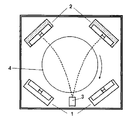
金属製のチャンバ壁(26)と、スパッタターゲットを有するマグネトロン(1,2)とを備えた真空チャンバからなり、
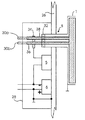
少なくとも一つのマグネトロンは、高電力パルスのマグネトロンスパッタリングプロセスで動作するHPPMSマグネトロン(1)として配されており、
スイッチング素子(5)を介して該HPPMSマグネトロン(1)のスパッタターゲットに容量素子(6)を接続することによって、電気パルスが該HPPMSマグネトロンに供給されている装置において、
該容量素子(6)は、並列接続したキャパシタからなる容量バンクとして構成され、
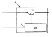
該スイッチング素子(5)と該容量素子(6)は、該チャンバ壁(26)の上に配されていることを特徴とする装置。 - 該HPPMSマグネトロンに対する電源供給のために、真空通路(8)が該チャンバ壁(26)に配されており、
該容量素子(6)、該スイッチング素子(5)及び該真空通路(8)はユニットを形成している
請求項1に記載の装置。 - 冷却手段が該HPPMSマグネトロンのために設けられており、
冷却媒体が導管(36,38)を通って該HPPMSマグネトロン(1)に流入し、
該導管(36,38)は、真空通路(8)を介して該チャンバ壁(26)を貫通しており、
該導管(36,38)が導電体として用いられ、該導電体により電流が該スイッチング素子(5)から該HPPMSマグネトロン(1)に導かれている
請求項1又は2に記載の装置。 - 冷却手段が該チャンバ壁及び/又は該チャンバ壁に取り付けられた真空通路のために設けられており、
該冷却手段が該スイッチング素子の冷却にも用いられる
請求項1,2又は3に記載の装置。 - 少なくとも一つの電極対が配されており、該電極対の少なくとも一つはHPPMSマグネトロン(1)であり、
電気配線が該電極対の各電極のために配されており、
該電極対の二つの電極のための該電気配線は、共通の真空通路(8)若しくは二つの隣接する真空通路を介して、コーテイング用の該チャンバに挿通しており、該電気配線は、該チャンバの内部で該電極に延びている
請求項1,2,3又は4に記載の装置。 - コーテイングされるべき物体を支持するための基板テーブル(4)と、
第1電極(1)及び第2電極(3)とを備えた少なくとも一つのプラズマ発生電極対を含み、
前記HPPMSマグネトロン(1)は該第1電極(1)であり、高電力パルスを用いたマグネトロンスパッタリングモードで動作し、
HPPMS電源が該第1電極と該第2電極との間に配されており、
該基板テーブル(4)に支持された物体が該電極対の能動面の間に位置するか、あるいは該電極対の能動面の間の空間を移動するように、該第1電極と該第2電極とを配置するようにした
請求項1,2,3,4又は5に記載の装置。 - 少なくとももう一つの電極対が真空チャンバに配されており、該電極対の各電極の少なくとも一つはマグネトロン(2)として構成されており、該マグネトロンは直流電源若しくは在来型のパルス電源に接続されている
請求項6に記載の装置。 - 該少なくとも一つの電極対の能動面の間の距離は20cmより大きい、
請求項6又は7に記載の装置。 - 該第2電極は、陽極(3)であり、
バイアス電圧を発生するために、バイアス電圧源(VB)が該陽極(3)と該基板テーブル(4)との間に配されている、
請求項6,7又は8に記載の装置。 - コーテイングの間プラズマにさらされる該陽極(3)の表面は、該プラズマにさらされる該第1電極の表面より小さい、
請求項9に記載の装置。 - 電源(VC)が該陽極と該チャンバ壁との間に配されており、コーテイングの間該チャンバ壁に対して該陽極を正電位に維持する
請求項9又は10に記載の装置。 - コーテイングの間、少なくとも二つのマグネトロンが共通の陽極(3)に対して接続されている
請求項9,10又は11に記載の装置。 - 該第2電極はHPPMSマグネトロン(1a)であり、
該第1電極と該第2電極との間にHPPMS電力供給源(40)が配されており、
このHPPMS電力供給源により、該電極(1,1a)が相互にバイポーラ方式でパルス駆動される
請求項6に記載の装置。 - マグネトロンスパッタリングにより物体を前処理及びコーテイングするための方法であって、
該物体は、金属製のチャンバ壁(26)と、スパッタターゲットを有するマグネトロンとを有する真空チャンバに配され、
該真空チャンバの中でプラズマが発生し、該スパッタターゲットの少なくとも一つがスパッタされ、
該マグネトロンの少なくとも一つは、高電力パルスを用いたマグネトロンスパッタリングプロセスによりHPPMSマグネトロンとして動作し、
スイッチング素子(5)を介して容量素子(6)を該HPPSマグネトロン(1)の該スパッタターゲットに接続することにより、電気パルスを該HPPSマグネトロン(1)に供給する方法において、
該容量素子(6)は、並列接続したキャパシタからなる容量バンクとして構成され、
該スイッチング素子(5)と該容量素子(6)が、該チャンバ壁(26)の上に配されていることを特徴とする方法。
Applications Claiming Priority (3)
| Application Number | Priority Date | Filing Date | Title |
|---|---|---|---|
| DE102008021128 | 2008-04-28 | ||
| DE102008021128.1 | 2008-04-28 | ||
| PCT/EP2009/003082 WO2009132822A2 (de) | 2008-04-28 | 2009-04-28 | Vorrichtung und verfahren zum vorbehandeln und beschichten von körpern |
Publications (3)
| Publication Number | Publication Date |
|---|---|
| JP2011518950A JP2011518950A (ja) | 2011-06-30 |
| JP2011518950A5 JP2011518950A5 (ja) | 2012-06-07 |
| JP5448232B2 true JP5448232B2 (ja) | 2014-03-19 |
Family
ID=40885977
Family Applications (1)
| Application Number | Title | Priority Date | Filing Date |
|---|---|---|---|
| JP2011505437A Active JP5448232B2 (ja) | 2008-04-28 | 2009-04-28 | 物体を前処理及びコーテイングするための装置及び方法 |
Country Status (6)
| Country | Link |
|---|---|
| US (1) | US9812299B2 (ja) |
| EP (1) | EP2272080B1 (ja) |
| JP (1) | JP5448232B2 (ja) |
| CN (1) | CN102027564B (ja) |
| DE (1) | DE202009018428U1 (ja) |
| WO (1) | WO2009132822A2 (ja) |
Families Citing this family (30)
| Publication number | Priority date | Publication date | Assignee | Title |
|---|---|---|---|---|
| DE102008050499B4 (de) | 2008-10-07 | 2014-02-06 | Systec System- Und Anlagentechnik Gmbh & Co. Kg | PVD-Beschichtungsverfahren, Vorrichtung zur Durchführung des Verfahrens und nach dem Verfahren beschichtete Substrate |
| DE202010001497U1 (de) * | 2010-01-29 | 2010-04-22 | Hauzer Techno-Coating B.V. | Beschichtungsvorrichtung mit einer HIPIMS-Leistungsquelle |
| JP5765627B2 (ja) * | 2010-09-27 | 2015-08-19 | 日立金属株式会社 | 耐久性に優れる被覆工具およびその製造方法 |
| EP2700083B1 (de) * | 2011-04-20 | 2015-04-22 | Oerlikon Surface Solutions AG, Trübbach | Verfahren zur bereistellung sequenzieller leistungspulse |
| DE102011117177A1 (de) | 2011-10-28 | 2013-05-02 | Oerlikon Trading Ag, Trübbach | Verfahren zur Bereitstellung sequenzieller Leistungspulse |
| BRPI1102335A2 (pt) | 2011-05-27 | 2013-06-25 | Mahle Metal Leve Sa | elemento dotado de pelo menos uma superfÍcie de deslizamento com um revestimento para uso em um motor de combustço interna ou em um compressor |
| WO2013045454A2 (en) * | 2011-09-30 | 2013-04-04 | Cemecon Ag | Coating of substrates using hipims |
| DE102011117994A1 (de) * | 2011-11-09 | 2013-05-16 | Oerlikon Trading Ag, Trübbach | HIPIMS-Schichten |
| JP5344204B2 (ja) * | 2012-03-05 | 2013-11-20 | 三菱マテリアル株式会社 | 表面被覆切削工具 |
| US9264150B2 (en) * | 2012-03-28 | 2016-02-16 | Globalfoundries Inc. | Reactive metal optical security device and methods of fabrication and use |
| DE102012013577A1 (de) | 2012-07-10 | 2014-01-16 | Oerlikon Trading Ag, Trübbach | Hochleistungsimpulsbeschichtungsmethode |
| US9126273B2 (en) | 2012-12-17 | 2015-09-08 | Kennametal Inc | Tool for the cutting machining of workpieces and process for coating substrate bodies |
| EP2784799B1 (en) * | 2013-03-28 | 2022-12-21 | CemeCon AG | Dense, hard coatings on substrates using HIPIMS |
| DE102013106351A1 (de) * | 2013-06-18 | 2014-12-18 | Innovative Ion Coatings Ltd. | Verfahren zur Vorbehandlung einer zu beschichtenden Oberfläche |
| US9677168B2 (en) | 2013-10-08 | 2017-06-13 | TPK America, LLC | Touch panel and method for manufacturing the same |
| US20150354054A1 (en) * | 2014-06-06 | 2015-12-10 | Applied Materials, Inc. | Cooled process tool adapter for use in substrate processing chambers |
| FR3025929B1 (fr) * | 2014-09-17 | 2016-10-21 | Commissariat Energie Atomique | Gaines de combustible nucleaire, procedes de fabrication et utilisation contre l'oxydation. |
| DE102014115492A1 (de) | 2014-10-24 | 2016-04-28 | Cemecon Ag | Verfahren und Vorrichtung zur Erzeugung einer elektronischen Entladung |
| US9812305B2 (en) * | 2015-04-27 | 2017-11-07 | Advanced Energy Industries, Inc. | Rate enhanced pulsed DC sputtering system |
| US11049702B2 (en) | 2015-04-27 | 2021-06-29 | Advanced Energy Industries, Inc. | Rate enhanced pulsed DC sputtering system |
| JP6871933B2 (ja) * | 2015-11-10 | 2021-05-19 | サンドビック インテレクチュアル プロパティー アクティエボラーグ | コーティングのための表面を前処理するための方法 |
| ES2883198T3 (es) | 2015-11-12 | 2021-12-07 | Oerlikon Surface Solutions Ag Pfaeffikon | Disposición de pulverización catódica y procedimiento para la distribución optimizada del flujo de energía |
| CN108291299B (zh) | 2015-11-27 | 2021-09-17 | 塞梅孔公司 | 用金刚石层和硬质材料层涂覆体 |
| US20180108519A1 (en) * | 2016-10-17 | 2018-04-19 | Applied Materials, Inc. | POWER DELIVERY FOR HIGH POWER IMPULSE MAGNETRON SPUTTERING (HiPIMS) |
| KR101885123B1 (ko) * | 2017-03-31 | 2018-08-03 | 한국알박(주) | 마그네트론 스퍼터링 장치의 자석 제어 시스템 |
| CN109112496B (zh) * | 2018-09-26 | 2020-11-24 | 武汉华星光电半导体显示技术有限公司 | 磁控溅射设备及去除基板上氧化层的方法 |
| DE102019124616A1 (de) | 2019-09-12 | 2021-03-18 | Cemecon Ag | Mehrlagige Beschichtung |
| US12325907B2 (en) | 2020-04-20 | 2025-06-10 | Joint-Stock Company “Tvel” | Method of ion-plasma application of corrosion-resistant film coatings on articles made from zirconium alloys |
| CN112708854A (zh) * | 2020-12-19 | 2021-04-27 | 合肥开泰机电科技有限公司 | 一种用于大面积钎焊的真空镀膜结构 |
| WO2023099757A1 (en) * | 2021-12-03 | 2023-06-08 | Université De Namur | A process for depositing a coating on a substrate by means of pvd methods and the coating obtained by said process |
Family Cites Families (21)
| Publication number | Priority date | Publication date | Assignee | Title |
|---|---|---|---|---|
| US3635811A (en) * | 1967-11-06 | 1972-01-18 | Warner Lambert Co | Method of applying a coating |
| US4098452A (en) * | 1975-03-31 | 1978-07-04 | General Electric Company | Lead bonding method |
| US5096562A (en) * | 1989-11-08 | 1992-03-17 | The Boc Group, Inc. | Rotating cylindrical magnetron structure for large area coating |
| US5962923A (en) * | 1995-08-07 | 1999-10-05 | Applied Materials, Inc. | Semiconductor device having a low thermal budget metal filling and planarization of contacts, vias and trenches |
| SE9704607D0 (sv) | 1997-12-09 | 1997-12-09 | Chemfilt R & D Ab | A method and apparatus for magnetically enhanced sputtering |
| GB9705022D0 (en) | 1997-03-11 | 1997-04-30 | James Alec C | Support means locatable so as to span a gap between two surfaces |
| WO1998046807A1 (en) * | 1997-04-14 | 1998-10-22 | Cemecon-Ceramic Metal Coatings-Dr.-Ing. Antonius Leyendecker Gmbh | Method and device for pvd coating |
| US20020046944A1 (en) * | 2000-06-28 | 2002-04-25 | Ehood Geva | Method and apparatus for reducing noise in a sputtering chamber |
| SE525231C2 (sv) | 2001-06-14 | 2005-01-11 | Chemfilt R & D Ab | Förfarande och anordning för att alstra plasma |
| JP4101554B2 (ja) * | 2001-08-17 | 2008-06-18 | 株式会社神戸製鋼所 | スパッタ装置及び方法 |
| US7172681B2 (en) * | 2003-02-05 | 2007-02-06 | Bridgestone Corporation | Process for producing rubber-based composite material |
| DE10318364A1 (de) * | 2003-04-23 | 2004-11-18 | Fraunhofer-Gesellschaft zur Förderung der angewandten Forschung e.V. | Einrichtung zum Beschichten eines stationär angeordneten Substrats durch Puls-Magnetron-Sputtern |
| US7663319B2 (en) * | 2004-02-22 | 2010-02-16 | Zond, Inc. | Methods and apparatus for generating strongly-ionized plasmas with ionizational instabilities |
| EP1609882A1 (de) | 2004-06-24 | 2005-12-28 | METAPLAS IONON Oberflächenveredelungstechnik GmbH | Kathodenzerstäubungsvorrichtung und -verfahren |
| SE0402644D0 (sv) | 2004-11-02 | 2004-11-02 | Biocell Ab | Method and apparatus for producing electric discharges |
| JP2006161088A (ja) * | 2004-12-06 | 2006-06-22 | Canon Inc | スパッタ装置 |
| US20060260938A1 (en) * | 2005-05-20 | 2006-11-23 | Petrach Philip M | Module for Coating System and Associated Technology |
| DE102005033769B4 (de) * | 2005-07-15 | 2009-10-22 | Systec System- Und Anlagentechnik Gmbh & Co.Kg | Verfahren und Vorrichtung zur Mehrkathoden-PVD-Beschichtung und Substrat mit PVD-Beschichtung |
| DE102006017382A1 (de) | 2005-11-14 | 2007-05-16 | Itg Induktionsanlagen Gmbh | Verfahren und Vorrichtung zum Beschichten und/oder zur Behandlung von Oberflächen |
| GB0608582D0 (en) * | 2006-05-02 | 2006-06-07 | Univ Sheffield Hallam | High power impulse magnetron sputtering vapour deposition |
| DE102006021994B4 (de) * | 2006-05-10 | 2017-08-03 | Cemecon Ag | Beschichtungsverfahren |
-
2009
- 2009-04-28 WO PCT/EP2009/003082 patent/WO2009132822A2/de not_active Ceased
- 2009-04-28 DE DE202009018428U patent/DE202009018428U1/de not_active Expired - Lifetime
- 2009-04-28 EP EP09737866A patent/EP2272080B1/de active Active
- 2009-04-28 CN CN200980115777XA patent/CN102027564B/zh active Active
- 2009-04-28 JP JP2011505437A patent/JP5448232B2/ja active Active
- 2009-04-28 US US12/989,882 patent/US9812299B2/en active Active
Also Published As
| Publication number | Publication date |
|---|---|
| CN102027564B (zh) | 2013-05-22 |
| WO2009132822A2 (de) | 2009-11-05 |
| DE202009018428U1 (de) | 2011-09-28 |
| JP2011518950A (ja) | 2011-06-30 |
| US9812299B2 (en) | 2017-11-07 |
| CN102027564A (zh) | 2011-04-20 |
| US20110180389A1 (en) | 2011-07-28 |
| EP2272080B1 (de) | 2012-08-01 |
| WO2009132822A3 (de) | 2010-01-21 |
| EP2272080A2 (de) | 2011-01-12 |
Similar Documents
| Publication | Publication Date | Title |
|---|---|---|
| JP5448232B2 (ja) | 物体を前処理及びコーテイングするための装置及び方法 | |
| EP2157205B1 (en) | A high-power pulsed magnetron sputtering process as well as a high-power electrical energy source | |
| US6413382B1 (en) | Pulsed sputtering with a small rotating magnetron | |
| JP4208970B2 (ja) | 交互に正電圧および負電圧にされる複数のアノードを用いる絶縁材料の連続堆積 | |
| EP2597172B1 (en) | Ion bombardment apparatus and method for cleaning of surface of base material using the same | |
| JP2011518950A5 (ja) | ||
| KR100260601B1 (ko) | 기판 코팅장치 | |
| JPH0841636A (ja) | 反応性スパッタ方法および装置 | |
| CN101589451A (zh) | 针对高功率脉冲磁控溅射(hipims)的rf衬底偏压 | |
| CN102308358A (zh) | 具有自清洁阳极的闭合漂移磁场离子源装置及基材改性修改方法 | |
| TW200830390A (en) | Method and apparatus for manufacturing cleaned substrates or clean substrates which are further processed | |
| JPH09186150A (ja) | 化学蒸着法により基板を被覆する装置 | |
| JP5649333B2 (ja) | イオンボンバードメント装置及びこの装置を用いた基材表面のクリーニング方法 | |
| EP0818801A2 (en) | Plasma treating apparatus | |
| JP7026464B2 (ja) | マグネトロンスパッタリング装置を用いて層を堆積させるための方法 | |
| US20080308410A1 (en) | Redundant Anode Sputtering Method and Assembly | |
| US20070144901A1 (en) | Pulsed cathodic arc plasma | |
| KR100480357B1 (ko) | 동기화된 이온 빔 소스와 듀얼 마그네트론 스퍼터를가지는 박막 형성 장치 | |
| JP4512311B2 (ja) | 真空処理プロセスのためのソースの操作方法 | |
| EP2159820B1 (en) | A physical vapour deposition coating device as well as a physical vapour deposition method | |
| JP6832572B2 (ja) | マグネトロンスパッタ法による装飾被膜の形成方法 | |
| JP7696292B2 (ja) | プラズマ処理を実行するためのプラズマ源のための磁石構成 | |
| KR101478216B1 (ko) | 이온 소스 및 이를 갖는 이온빔 처리 장치 | |
| EP2607517A1 (en) | Low temperature arc ion plating coating | |
| CN110468379A (zh) | 一种配置热丝的电弧离子镀膜装置 |
Legal Events
| Date | Code | Title | Description |
|---|---|---|---|
| A521 | Request for written amendment filed |
Free format text: JAPANESE INTERMEDIATE CODE: A523 Effective date: 20120420 |
|
| A621 | Written request for application examination |
Free format text: JAPANESE INTERMEDIATE CODE: A621 Effective date: 20120420 |
|
| A977 | Report on retrieval |
Free format text: JAPANESE INTERMEDIATE CODE: A971007 Effective date: 20130704 |
|
| A131 | Notification of reasons for refusal |
Free format text: JAPANESE INTERMEDIATE CODE: A131 Effective date: 20130710 |
|
| A601 | Written request for extension of time |
Free format text: JAPANESE INTERMEDIATE CODE: A601 Effective date: 20130928 |
|
| A602 | Written permission of extension of time |
Free format text: JAPANESE INTERMEDIATE CODE: A602 Effective date: 20131007 |
|
| A521 | Request for written amendment filed |
Free format text: JAPANESE INTERMEDIATE CODE: A523 Effective date: 20131107 |
|
| TRDD | Decision of grant or rejection written | ||
| A01 | Written decision to grant a patent or to grant a registration (utility model) |
Free format text: JAPANESE INTERMEDIATE CODE: A01 Effective date: 20131203 |
|
| A61 | First payment of annual fees (during grant procedure) |
Free format text: JAPANESE INTERMEDIATE CODE: A61 Effective date: 20131221 |
|
| R150 | Certificate of patent or registration of utility model |
Ref document number: 5448232 Country of ref document: JP Free format text: JAPANESE INTERMEDIATE CODE: R150 Free format text: JAPANESE INTERMEDIATE CODE: R150 |
|
| R250 | Receipt of annual fees |
Free format text: JAPANESE INTERMEDIATE CODE: R250 |
|
| R250 | Receipt of annual fees |
Free format text: JAPANESE INTERMEDIATE CODE: R250 |
|
| R250 | Receipt of annual fees |
Free format text: JAPANESE INTERMEDIATE CODE: R250 |
|
| R250 | Receipt of annual fees |
Free format text: JAPANESE INTERMEDIATE CODE: R250 |
|
| R250 | Receipt of annual fees |
Free format text: JAPANESE INTERMEDIATE CODE: R250 |
|
| R250 | Receipt of annual fees |
Free format text: JAPANESE INTERMEDIATE CODE: R250 |
|
| R250 | Receipt of annual fees |
Free format text: JAPANESE INTERMEDIATE CODE: R250 |
|
| R250 | Receipt of annual fees |
Free format text: JAPANESE INTERMEDIATE CODE: R250 |
|
| R250 | Receipt of annual fees |
Free format text: JAPANESE INTERMEDIATE CODE: R250 |
|
| R250 | Receipt of annual fees |
Free format text: JAPANESE INTERMEDIATE CODE: R250 |