JP6062155B2 - Ge-rich GST-212 phase change material - Google Patents
Ge-rich GST-212 phase change material Download PDFInfo
- Publication number
- JP6062155B2 JP6062155B2 JP2012103247A JP2012103247A JP6062155B2 JP 6062155 B2 JP6062155 B2 JP 6062155B2 JP 2012103247 A JP2012103247 A JP 2012103247A JP 2012103247 A JP2012103247 A JP 2012103247A JP 6062155 B2 JP6062155 B2 JP 6062155B2
- Authority
- JP
- Japan
- Prior art keywords
- gst
- phase change
- change memory
- memory material
- range
- Prior art date
- Legal status (The legal status is an assumption and is not a legal conclusion. Google has not performed a legal analysis and makes no representation as to the accuracy of the status listed.)
- Active
Links
Images


Classifications
-
- H—ELECTRICITY
- H10—SEMICONDUCTOR DEVICES; ELECTRIC SOLID-STATE DEVICES NOT OTHERWISE PROVIDED FOR
- H10N—ELECTRIC SOLID-STATE DEVICES NOT OTHERWISE PROVIDED FOR
- H10N70/00—Solid-state devices without a potential-jump barrier or surface barrier, and specially adapted for rectifying, amplifying, oscillating or switching
- H10N70/20—Multistable switching devices, e.g. memristors
- H10N70/231—Multistable switching devices, e.g. memristors based on solid-state phase change, e.g. between amorphous and crystalline phases, Ovshinsky effect
-
- C—CHEMISTRY; METALLURGY
- C23—COATING METALLIC MATERIAL; COATING MATERIAL WITH METALLIC MATERIAL; CHEMICAL SURFACE TREATMENT; DIFFUSION TREATMENT OF METALLIC MATERIAL; COATING BY VACUUM EVAPORATION, BY SPUTTERING, BY ION IMPLANTATION OR BY CHEMICAL VAPOUR DEPOSITION, IN GENERAL; INHIBITING CORROSION OF METALLIC MATERIAL OR INCRUSTATION IN GENERAL
- C23C—COATING METALLIC MATERIAL; COATING MATERIAL WITH METALLIC MATERIAL; SURFACE TREATMENT OF METALLIC MATERIAL BY DIFFUSION INTO THE SURFACE, BY CHEMICAL CONVERSION OR SUBSTITUTION; COATING BY VACUUM EVAPORATION, BY SPUTTERING, BY ION IMPLANTATION OR BY CHEMICAL VAPOUR DEPOSITION, IN GENERAL
- C23C16/00—Chemical coating by decomposition of gaseous compounds, without leaving reaction products of surface material in the coating, i.e. chemical vapour deposition [CVD] processes
- C23C16/22—Chemical coating by decomposition of gaseous compounds, without leaving reaction products of surface material in the coating, i.e. chemical vapour deposition [CVD] processes characterised by the deposition of inorganic material, other than metallic material
- C23C16/30—Deposition of compounds, mixtures or solid solutions, e.g. borides, carbides, nitrides
- C23C16/305—Sulfides, selenides, or tellurides
-
- C—CHEMISTRY; METALLURGY
- C30—CRYSTAL GROWTH
- C30B—SINGLE-CRYSTAL GROWTH; UNIDIRECTIONAL SOLIDIFICATION OF EUTECTIC MATERIAL OR UNIDIRECTIONAL DEMIXING OF EUTECTOID MATERIAL; REFINING BY ZONE-MELTING OF MATERIAL; PRODUCTION OF A HOMOGENEOUS POLYCRYSTALLINE MATERIAL WITH DEFINED STRUCTURE; SINGLE CRYSTALS OR HOMOGENEOUS POLYCRYSTALLINE MATERIAL WITH DEFINED STRUCTURE; AFTER-TREATMENT OF SINGLE CRYSTALS OR A HOMOGENEOUS POLYCRYSTALLINE MATERIAL WITH DEFINED STRUCTURE; APPARATUS THEREFOR
- C30B29/00—Single crystals or homogeneous polycrystalline material with defined structure characterised by the material or by their shape
- C30B29/10—Inorganic compounds or compositions
- C30B29/46—Sulfur-, selenium- or tellurium-containing compounds
-
- H—ELECTRICITY
- H10—SEMICONDUCTOR DEVICES; ELECTRIC SOLID-STATE DEVICES NOT OTHERWISE PROVIDED FOR
- H10N—ELECTRIC SOLID-STATE DEVICES NOT OTHERWISE PROVIDED FOR
- H10N70/00—Solid-state devices without a potential-jump barrier or surface barrier, and specially adapted for rectifying, amplifying, oscillating or switching
- H10N70/011—Manufacture or treatment of multistable switching devices
- H10N70/021—Formation of the switching material, e.g. layer deposition
- H10N70/026—Formation of the switching material, e.g. layer deposition by physical vapor deposition, e.g. sputtering
-
- H—ELECTRICITY
- H10—SEMICONDUCTOR DEVICES; ELECTRIC SOLID-STATE DEVICES NOT OTHERWISE PROVIDED FOR
- H10N—ELECTRIC SOLID-STATE DEVICES NOT OTHERWISE PROVIDED FOR
- H10N70/00—Solid-state devices without a potential-jump barrier or surface barrier, and specially adapted for rectifying, amplifying, oscillating or switching
- H10N70/801—Constructional details of multistable switching devices
- H10N70/821—Device geometry
- H10N70/826—Device geometry adapted for essentially vertical current flow, e.g. sandwich or pillar type devices
-
- H—ELECTRICITY
- H10—SEMICONDUCTOR DEVICES; ELECTRIC SOLID-STATE DEVICES NOT OTHERWISE PROVIDED FOR
- H10N—ELECTRIC SOLID-STATE DEVICES NOT OTHERWISE PROVIDED FOR
- H10N70/00—Solid-state devices without a potential-jump barrier or surface barrier, and specially adapted for rectifying, amplifying, oscillating or switching
- H10N70/801—Constructional details of multistable switching devices
- H10N70/881—Switching materials
- H10N70/882—Compounds of sulfur, selenium or tellurium, e.g. chalcogenides
- H10N70/8828—Tellurides, e.g. GeSbTe
Description
本技術は、相変化メモリベースの材料に基づいて、高密度メモリデバイスに関する。 The present technology relates to high density memory devices based on phase change memory based materials.
相変化メモリベースの材料は、カルコゲナイド系材料及び類似の材料のように、集積回路の実装に適したレベルにおいて、電流の応用による非結晶状態と結晶状態との間の位相を変化させることができる。通常の非結晶状態は、通常の結晶状態よりも高い電気抵抗を有することを特徴とし、データを示すように容易に検出できる。これらの特性は、プログラム可能な抵抗材料を使用して不揮発性メモリ回路を形成する関心を引き起こし、ランダムアクセスで読み取む、又は書き込むことができる。 Phase change memory-based materials, like chalcogenide-based materials and similar materials, can change the phase between the amorphous and crystalline states due to the application of current at a level suitable for integrated circuit implementation. . The normal amorphous state is characterized by having a higher electrical resistance than the normal crystalline state and can be easily detected as shown in the data. These characteristics create interest in using programmable resistive materials to form non-volatile memory circuits and can be read or written with random access.
一般的には、非結晶状態から結晶状態までの変化は、より低い電流操作である。結晶状態から非結晶状態までの変化は、リセットと呼ばれ、一般的により高い電流操作であり、短い高電流密度パルスを含んで結晶構造を融解または破壊する。その後、相変化材料を迅速に冷却し、相変化プロセスを急冷し、相変化材料の少なくとも一部を、非結晶状態を安定化する。 In general, the change from an amorphous state to a crystalline state is a lower current operation. The change from the crystalline state to the non-crystalline state is called reset and is generally a higher current manipulation that involves short high current density pulses to melt or destroy the crystalline structure. Thereafter, the phase change material is rapidly cooled, the phase change process is quenched, and at least a portion of the phase change material is stabilized in an amorphous state.
相変化メモリでは、データが非結晶と結晶状態との間の相変化材料の活性領域における変化を引き起こすことによって格納されている。低抵抗の結晶セット状態の最高抵抗R1と高抵抗の非結晶リセット状態の最低抵抗R2との差異は、非結晶リセット状態から結晶セット状態におけるセルを区別するように使用されるリードマージン(read margin)を定義する。メモリセルに格納されたデータは、メモリセルが低抵抗状態または高抵抗状態に対応する抵抗を有するかどうかを決定することにより、例えば、メモリセルの抵抗値がリードマージン内の抵抗しきい値よりも高い又は低いかどうかを測定することにより決定される。 In phase change memory, data is stored by causing a change in the active region of the phase change material between the amorphous and crystalline states. The difference between the highest resistance R1 in the low resistance crystal set state and the lowest resistance R2 in the high resistance amorphous reset state is the read margin used to distinguish cells in the crystal set state from the amorphous reset state. ) Is defined. The data stored in the memory cell is determined by determining whether the memory cell has a resistance corresponding to the low resistance state or the high resistance state, for example, the resistance value of the memory cell is greater than the resistance threshold value within the read margin. Is also determined by measuring whether it is high or low.
GST−225族内の材料は、“GeSbTe三元合金の構造,電気,及び動力学パラメータ”(E.MORALES−SANCHEZ、Thin Solid Films471(2005)243−247)で報告されたSb2Te3とGeTeタイラインに沿うGeSbTe組成物を含む。GST−225族内の材料から製造される従来の相変化メモリセルは、上昇する温度で非結晶リセット状態から結晶セット状態に望ましくない変化を得ることが観察されている。上昇する温度でのアレイ内のメモリセルの活性領域内の相変化材料の望ましくない変化は、誤りデータの作成及び格納されたいデータの損失が得られる。GST−225の相変化メモリセルの熱安定性を向上させるための努力は、より遅いセットとリセット速度で、より高いリセット電流によって操作し、結晶セット状態の低抵抗と非結晶状態の高抵抗との差異の減少を有している。 Materials within the GST-225 group are Sb2Te3 and GeTe tie lines reported in “GeSbTe ternary alloy structural, electrical, and kinetic parameters” (E. MORALES-SANCHEZ, Thin Solid Films 471 (2005) 243-247). A GeSbTe composition along Conventional phase change memory cells fabricated from materials within the GST-225 family have been observed to obtain undesirable changes from the amorphous reset state to the crystalline set state at increasing temperatures. Undesirable changes in the phase change material in the active region of the memory cells in the array at increasing temperatures can result in the creation of erroneous data and the loss of data to be stored. Efforts to improve the thermal stability of GST-225 phase change memory cells are operated with higher reset current at slower set and reset speed, and low resistance in crystalline set state and high resistance in amorphous state. Have a decrease in the difference.
上昇操作温度で非結晶リセット状態から結晶セット状態に望ましくない変化を防止するために、高い結晶化温度を有する相変化メモリ材料を提供することが望ましい。相変化メモリ材料は、リセット状態の抵抗値範囲とセット状態の抵抗値範囲との大きな差異を維持することがさらに望ましい。相変化メモリ材料は、高いセット及びリセット速度を維持しながら、高い結晶化温度を有することも望ましい。最後に、相変化メモリ材料は、従来のGST−225相変化メモリ材料よりも低リセット電流で設定され、セット結晶状態からリセット結晶状態に変化することができることが望ましい。 In order to prevent undesired changes from the amorphous reset state to the crystal set state at elevated operating temperatures, it is desirable to provide a phase change memory material having a high crystallization temperature. It is further desirable for the phase change memory material to maintain a large difference between the resistance value range in the reset state and the resistance value range in the set state. It is also desirable for the phase change memory material to have a high crystallization temperature while maintaining a high set and reset rate. Finally, it is desirable that the phase change memory material is set with a lower reset current than the conventional GST-225 phase change memory material and can change from the set crystal state to the reset crystal state.
本発明の主な目的は、GeリッチなGST−212相変化材料を提供することにより、従来のGST−225の相変化メモリよりも高い結晶化温度、低いリセット電流要件及び優れた保持率を有することができる。 The main objective of the present invention is to provide a Ge-rich GST-212 phase change material, thereby having higher crystallization temperature, lower reset current requirement and better retention than conventional GST-225 phase change memory. be able to.
GST−212族の材料及びGeリッチなGST−212族の材料における相変化メモリ材料は、当技術分野で使用された典型的なGST−225の相変化メモリよりも高い結晶化温度、低いリセット電流要件及び優れた保持率を有することができる。GST−212族内の材料は、170°Cより高い結晶化温度を有している。前記材料は、GST−225の相変化メモリ材料に比べて、速いセット速度を有しながら、高い結晶化温度を維持する。 Phase change memory materials in GST-212 and Ge-rich GST-212 materials have higher crystallization temperatures, lower reset currents than typical GST-225 phase change memories used in the art. Can have requirements and excellent retention. Materials within the GST-212 group have a crystallization temperature higher than 170 ° C. The material maintains a high crystallization temperature while having a faster set speed compared to the GST-225 phase change memory material.
GST−212族内の相変化メモリ材料は、GST−225族内の材料に比べて、減少されたリセット電流を有している。本明細書に記載されている相変化メモリ材料は、バックエンドオブライン(BEOL)処理中の上昇温度に暴露された後、粒径に大きな間隙を形成しなく且つ大きな変動を保持しない。さらに、本明細書に記載されている相変化メモリ材料は、上昇温度に暴露が延長された後、非結晶リセット状態に維持する。 Phase change memory materials in the GST-212 group have a reduced reset current compared to materials in the GST-225 group. The phase change memory materials described herein do not form large gaps in particle size and retain large fluctuations after exposure to elevated temperatures during back-end-of-line (BEOL) processing. Further, the phase change memory materials described herein remain in an amorphous reset state after extended exposure to elevated temperatures.
GST−212族内の相変化メモリ材料は、上昇温度で操作サイクルが繰り返された後、非結晶リセット状態の高抵抗と結晶セット状態の低抵抗との間の抵抗値に大きな差を維持する。GST−212族内の材料は、生成支配機構により結晶化され、対照的に、GST−225族内の材料は、核生成支配機構により結晶化される。 Phase change memory materials within the GST-212 family maintain a large difference in resistance values between the high resistance in the amorphous reset state and the low resistance in the crystal set state after repeated operating cycles at elevated temperatures. Materials within the GST-212 group are crystallized by a production-dominated mechanism, in contrast, materials within the GST-225 group are crystallized by a nucleation-dominated mechanism.
GST−212族からの相変化メモリ材料から製造されたメモリセル装置は、本明細書に記載されているGST−225よりも高い結晶化温度を有する。メモリセル装置は、メモリセルのアレイが含まれている。各メモリセルは、メモリセルのメモリ素子に結合された第一電極及び第二電極を含む。メモリ素子は、セットとリセット状態との間の相変化が実質的に発生する活性領域を含む。 Memory cell devices fabricated from phase change memory materials from the GST-212 family have a higher crystallization temperature than GST-225 described herein. The memory cell device includes an array of memory cells. Each memory cell includes a first electrode and a second electrode coupled to a memory element of the memory cell. The memory device includes an active region where a phase change between the set and reset states occurs substantially.
本明細書に記載されているメモリセル装置の製造方法は、GST−225よりも高い結晶化温度を有する相変化メモリ材料を使用する。 The method of manufacturing a memory cell device described herein uses a phase change memory material that has a higher crystallization temperature than GST-225.
本願明細書に記載された技術の他の態様及び利点は、以下の図面、発明の詳細説明及び特許請求範囲に見ることができる。 Other aspects and advantages of the techniques described herein can be found in the following drawings, detailed description of the invention, and the claims.
本発明は、GeリッチなGST−212相変化材料の組成を改善することにより、GST−225の相変化メモリよりも高い結晶化温度、低いリセット電流要件及び優れた保持率を有することができる。 The present invention can have a higher crystallization temperature, lower reset current requirement and better retention than GST-225 phase change memory by improving the composition of Ge-rich GST-212 phase change material.
以下のように、本発明を実施例に基づいて詳述するが、あくまでも例示であって、本発明の範囲はこれらの実施形態に限定されない。本発明の範囲は、特許請求の範囲に記載されており、さらに特許請求の範囲の記載と均等な意味及び範囲内での全ての変更を含んでいる。 As described below, the present invention will be described in detail based on examples. However, the present invention is merely illustrative, and the scope of the present invention is not limited to these embodiments. The scope of the present invention is described in the scope of the claims, and includes all modifications within the meaning and scope equivalent to the scope of the claims.
本発明の実施形態に係る詳細な説明は、図1から図22を参照して提供されている。 A detailed description of embodiments of the present invention is provided with reference to FIGS.
図1は、様々な原子パーセント濃度で、点位置のグレースケールコーディングを使用する結晶化温度を示す三元系相図であり、その点位置は、GeSbTe(以下にはGST)組成物に対応する。本発明の一実施形態に係る高い結晶化温度の組成物は、一般的にGe/Sb2Te3対応線104に沿って配置されており、Ge2Sb1Te2に似ている(Ge2Sb1Te2を包含する)濃度を有する材料を含む。ここに呼ばれる"GST−212族"の材料グループは、形状102に含まれ、GexSbyTez族を含む。その中、Geの原子パーセント濃度は、30%〜65%の範囲内にあり、Sb原子パーセント濃度は、13%〜27%の範囲内にあり、Te原子パーセント濃度は、20%〜45%の範囲内にある。
FIG. 1 is a ternary phase diagram showing crystallization temperatures using gray scale coding of point positions at various atomic percent concentrations, the point positions corresponding to GeSbTe (hereinafter GST) compositions. . The high crystallization temperature composition according to one embodiment of the present invention is generally disposed along the Ge /
ここに呼ばれる"GeリッチなGST−212族"の材料グループは、形状102によって包含され、ここで、Geの最小濃度は40%である。本明細書に記載されたGeリッチなGST−212族内での材料は、200°Cを超える結晶化温度を有し、その結晶化温度は、典型的なGST−225族の材料よりも少なくとも50℃以上を超える。さらに、本明細書に記載の材料は、典型的なGST−225族の材料よりも約30%低いリセット電流で操作可能である。
The “Ge-rich GST-212” material group referred to here is encompassed by
新しい相変化材料を発展させるための重要な原因は、相変化材料の抵抗である。装置が必要とするリセット電流を決定するため、結晶状態の抵抗値が特に重要である。GST−225の場合には、結晶状態の抵抗が非常に低いため、非常に高いリセット電流を必要としてリセットされる。発明者は、GST−212族とGeリッチなGST−212族を発見した。より高いGe濃度は、結晶状態の高抵抗に導くため、低いリセット電流を必要とする。 An important cause for developing new phase change materials is the resistance of the phase change material. In order to determine the reset current required by the device, the resistance value of the crystalline state is particularly important. In the case of GST-225, since the resistance in the crystal state is very low, the reset is performed by requiring a very high reset current. The inventor has discovered the GST-212 family and the Ge-rich GST-212 family. A higher Ge concentration requires a low reset current because it leads to a high resistance in the crystalline state.
したがって、GeリッチなGST−212の抵抗値は、GST−212の抵抗値に近い、又、両方は、GeプアなGST−212よりも大きい抵抗を有している。GeリッチなGST−212のリセット電流は、GST−212のリセット電流に近い、両方は、GeプアなGST−212よりも低いリセット電流を有している。GST−212およびGeリッチなGST−212の比較について、転移温度Txは、GeリッチなGST−212の方が高くなるため、保持を更に向上させることができる。 Therefore, the resistance value of Ge-rich GST-212 is close to that of GST-212, and both have higher resistance than Ge poor GST-212. The Ge-rich GST-212 reset current is close to the GST-212 reset current, both have a lower reset current than the Ge poor GST-212. Regarding the comparison between GST-212 and Ge-rich GST-212, since the transition temperature Tx is higher in Ge-rich GST-212, the retention can be further improved.
GST−225と比較し、十分に速い速度(GST−225よりも遅いが、それでも十分に速い)を有する時、GeリッチなGST−212は、高いTx及び結晶状態の高抵抗を有する材料であり、低いリセット電流と優れた耐久性と組み合わせて成る。 Ge-rich GST-212 is a material with high Tx and high resistance in the crystalline state when it has a sufficiently fast speed (slower than GST-225 but still fast enough) compared to GST-225. Combining low reset current and excellent durability.
GeリッチなGST−212の材料は、Ge−Sb2Te3相図対応線104の周りに最も高いGe濃度側での点にある材料を含み、前記対応線104が相図でのGe2Sb1Te2の点に通じる。図1に示されたGeリッチなGST−212の材料は、形状102によって包含されるエリア内にある組成物を有する材料であり、前記材料は、200℃以上の結晶化温度を有することになる。代表的な組成物は、図1に示された位置105でのGeSbTe系材料であり、Ge原子パーセント濃度は約42.9%であり、Sb原子パーセント濃度は、約20.5%であり、Te原子パーセント濃度は、約36.6%であり(以下の「代表的な組成物」)、テストで優れた特性を示している。このような代表的な組成の向上させるパフォーマンス特性は、約250℃での結晶化温度を含む。増加した結晶化温度は、上昇温度でのデータ保持及び装置のパフォーマンスを向上させる。さらに、向上させるパフォーマンス特性は、GST−225族の材料から製造されたメモリ装置に必要なリセット電流よりも30%少ないリセット電流が含まれている。減少したリセット電流は、低い電力レベルでも簡単な装置のプログラミングを可能にする。
The Ge-rich GST-212 material includes the material at the highest Ge concentration point around the Ge-Sb2Te3 phase
GST−225族の材料は、図1に示され、楕円形108によって包含されるエリア内にある組成物を有する材料である。このようなGST−225族の材料は、三元系相図でのSb2Te3−GeTe対応線に沿って又は近づいているGeSbTe組成物を含む。前記三元系相図に示すように、GST−225族内の材料の組成物は、150℃以下の結晶化温度を有している。より高い温度で操作される相変化メモリ装置には、このような低結晶化温度は、減少するデータ保持が得られる。温度が増加すると、非結晶相変化材料の部分は、非結晶リセット状態から結晶セット状態に結晶化する。データを格納するために使用される相変化材料の結晶セット状態と非結晶リセット状態との間の抵抗率は異なる。従って、メモリセル内の相変化材料は上昇温度で非結晶から結晶状態に変化すると、誤りデータが作成され、メモリ装置内に保存される。さらに、上昇温度での非晶質から結晶状態までの変化は、必要な格納されているデータの損失に導く。故に、低い結晶化温度は、メモリ装置内の乏しいデータ保持及び必要なメモリ装置のパフォーマンス特性の劣化に繋がる。 A GST-225 material is a material having a composition that is within the area shown in FIG. Such GST-225 materials include GeSbTe compositions that are along or approaching the Sb2Te3-GeTe corresponding line in the ternary phase diagram. As shown in the ternary phase diagram, the composition of the material within the GST-225 group has a crystallization temperature of 150 ° C. or lower. For phase change memory devices operated at higher temperatures, such low crystallization temperatures provide reduced data retention. As the temperature increases, the portion of the amorphous phase change material crystallizes from the amorphous reset state to the crystal set state. The resistivity between the crystalline set state and the amorphous reset state of the phase change material used to store the data is different. Therefore, when the phase change material in the memory cell changes from an amorphous state to a crystalline state at an elevated temperature, error data is created and stored in the memory device. Furthermore, the change from amorphous to crystalline state at elevated temperatures leads to the loss of necessary stored data. Thus, a low crystallization temperature leads to poor data retention in the memory device and degradation of the required memory device performance characteristics.
増加した結晶化温度は、GeプアなGST−212族内の材料に観察される。GeプアなGST−212族内の材料は、図1に示す形状102内に、30%〜40%の範囲内にあるGeの原子パーセント濃度を有する材料を含む。GeプアなGST−212族内の材料は、GeリッチなGST−212族の材料のような結晶化温度を劇的に上昇することを有していない。しかし、GeプアなGST−212族内の材料は、依然として170℃から200℃までの間の結晶化温度を有している。
Increased crystallization temperature is observed for materials within the Ge poor GST-212 group. Materials within the Ge Poor GST-212 group include materials having an atomic percent concentration of Ge in the range of 30% to 40% within the
本明細書に記載された材料は、ドープされたカルコゲナイドを用いて、導電性、転移温度、融解温度、及びメモリ素子の他の特性を変更するように、不純物をドープすることができる。カルコゲナイドのドーピングに使用される代表的な不純物は、例えば米国特許第6800504、米国特許第7893419を参照し、窒素、ケイ素、酸素、二酸化ケイ素、窒化ケイ素、銅、銀、金、アルミニウム、酸化アルミニウム、タンタル、酸化タンタル、窒化タンタル、チタン及びチタン酸化物が含まれている。したがって、GST−212族内の材料は、結晶化温度を更に高め、リセット電流を下げ、他の所望の材料の性能面を向上させるように、不純物をドープすることができる。 The materials described herein can be doped with impurities to use doped chalcogenides to alter conductivity, transition temperature, melting temperature, and other properties of the memory element. Typical impurities used for chalcogenide doping are described in, for example, US Pat. No. 6,800,504, US Pat. No. 7,893,419, nitrogen, silicon, oxygen, silicon dioxide, silicon nitride, copper, silver, gold, aluminum, aluminum oxide, Tantalum, tantalum oxide, tantalum nitride, titanium and titanium oxide are included. Therefore, materials within the GST-212 group can be doped with impurities to further increase the crystallization temperature, lower the reset current, and improve the performance aspects of other desired materials.
GeリッチなGST−212族内の材料は、図1に示すように、GST−225族の材料よりも高い結晶化温度を有している。GeリッチなGST−212族内の代表的な材料は、約200℃〜315℃までの範囲の結晶化温度を有している。GeリッチなGST−212族内の材料のより高い結晶化温度は、装置パフォーマンスの改善及びデータ保持が得られる。具体的には、上昇操作温度での相変化メモリ材料は、非結晶リセット状態から結晶セット状態に変化させなく、この変化は、誤りデータの作成及び望ましい保存データの損失により、好ましいパフォーマンス特性の低下が得られる。 As shown in FIG. 1, the Ge-rich GST-212 material has a higher crystallization temperature than the GST-225 material. Exemplary materials within the Ge-rich GST-212 group have crystallization temperatures ranging from about 200 ° C to 315 ° C. Higher crystallization temperatures of materials within the Ge-rich GST-212 group provide improved device performance and data retention. Specifically, phase change memory materials at elevated operating temperatures do not change from an amorphous reset state to a crystal set state, which is a reduction in favorable performance characteristics due to the creation of erroneous data and the loss of desirable stored data. Is obtained.
図2は、GST−225(軌跡124)、GST−212(軌跡120)、GeプアなGST−212(軌跡123)、及びGeリッチなGST−212の組成の抵抗対温度曲線(軌跡122)を比較する。より高い転移温度Txに加えて、GeリッチなGST−212族の代表的な組成物は、結晶状態でGST−225よりも高い抵抗を示し、リセット電流を減らすことができる。 FIG. 2 shows resistance versus temperature curves (trajectory 122) for compositions of GST-225 (trajectory 124), GST-212 (trajectory 120), Ge poor GST-212 (trajectory 123), and Ge-rich GST-212. Compare. In addition to the higher transition temperature Tx, the Ge-rich representative group GST-212 composition exhibits a higher resistance than GST-225 in the crystalline state and can reduce the reset current.
GST−225の抵抗率(124)は、約150℃の温度で劇的に減少し始め、GST−225の結晶化温度は約150℃であることを示している。GST−212の抵抗率(120)は、約200℃の温度で劇的に減少し始め、GST−212の結晶化温度は約200℃であることを示し、GST−225よりも約50℃高い結晶化温度があるため、上昇温度で所望のパフォーマンス特性及び改良されたデータ保持を実現する。GeリッチなGST−212族(124)内の代表的な組成物の抵抗は、約250℃の温度で劇的に減少し始め、約250℃の結晶化温度を示している。 The resistivity (124) of GST-225 begins to decrease dramatically at a temperature of about 150 ° C., indicating that the crystallization temperature of GST-225 is about 150 ° C. The resistivity (120) of GST-212 begins to decrease dramatically at a temperature of about 200 ° C., indicating that the crystallization temperature of GST-212 is about 200 ° C., about 50 ° C. higher than GST-225. Because of the crystallization temperature, the desired performance characteristics and improved data retention are achieved at elevated temperatures. The resistance of a typical composition within Ge-rich GST-212 (124) begins to decrease dramatically at a temperature of about 250 ° C., indicating a crystallization temperature of about 250 ° C.
結晶セット状態から非結晶リセット状態にGST−212族内の材料を変換するために、必要とされるリセット電流は、GST−225族内の材料のためのリセット電流よりも約30%少なくなる。リセット電流は、結晶セット状態から非結晶リセット状態に相変化メモリ材料を変化させるために必要な電流量である。このリセット電流は、結晶化材料の一部が溶けるように、相変化メモリ材料の温度を最大溶融温度に変化させる。相変化材料の溶融部は、迅速に急冷することによって非結晶リセット状態に固化する。あるいは、セット電流は、非結晶リセット状態から結晶セット状態に相変化メモリ材料を変化させるために必要な電流量である。セット電流は、相変化メモリ材料を、最大の溶融温度を超えないように、非結晶リセット状態から結晶セット状態に変化させるため、相変化メモリ材料は、非結晶リセット状態から結晶化する。 In order to convert the material in the GST-212 group from the crystal set state to the amorphous reset state, the reset current required is about 30% less than the reset current for the material in the GST-225 group. The reset current is an amount of current necessary to change the phase change memory material from the crystal set state to the amorphous reset state. This reset current changes the temperature of the phase change memory material to the maximum melting temperature so that a portion of the crystallized material melts. The melted portion of the phase change material is solidified into an amorphous reset state by rapidly quenching. Alternatively, the set current is the amount of current required to change the phase change memory material from the amorphous reset state to the crystal set state. The set current changes the phase change memory material from the amorphous reset state to the crystal set state so that the maximum melting temperature is not exceeded, so the phase change memory material crystallizes from the amorphous reset state.
図2に示すように、結晶セット状態128でのGST−225材料の抵抗は、0.01Ω-cmの以下である。結晶セット状態130におけるGST−212材料の抵抗及び結晶セット状態132におけるGeリッチなGST−212族の代表的な組成物の抵抗は、温度の全範囲にわたって、0.01Ω-cm以上(約0.05Ω-cm)に維持する。結晶状態におけるGST−212族内の材料の抵抗は、GST−225族内の材料よりも高くなり、GST−212およびGeリッチなGST−212族の代表的な組成物の両方を含む。従って、結晶セット状態から非結晶リセット状態に材料を変化させるために、低いリセット電流の必要がある。故に、GST−212族内の材料は、GST−225族内の材料よりも30%低いリセット電流を有することができる。
As shown in FIG. 2, the resistance of the GST-225 material in the
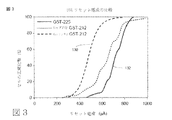
図3は、GeリッチなGST−212族の材料の低いリセット電流を示し、様々なGST組成物のためのセルの正規化数関数としてのリセット電流のプロットである。130で表され、GeリッチなGST−212族の代表的な組成物から製造されたセルの正規化数のリセット電流は、132で表されるGST−225の材料から製造されたセルの正規化数のリセット電流よりも低くなる。 FIG. 3 shows the low reset current for Ge-rich GST-212 material and is a plot of reset current as a function of cell normalization for various GST compositions. The reset current of a normalized number of cells represented by 130 and manufactured from a representative composition of the Ge-rich GST-212 family is normalized for cells manufactured from the GST-225 material represented by 132. Lower than the reset current of the number.
具体的には、GeリッチなGST−212から製造されたセルの50%の正規化数のリセット電流は、450μA程度である。GST−225から製造されたセルの50%の正規化数のリセット電流は、700μA程度である。GeリッチなGST−212とGST−225との間のリセット電流の差異は、正規化されたセルの割合の全範囲にわたって一定のままである。したがって、GeリッチなGST−212族のセットからリセット状態に材料を変化させるために、必要とされるリセット電流は、テストされたGST−225族内の材料のリセット電流よりも約30%少なくなる。 Specifically, the reset current for a normalized number of 50% of cells made from Ge-rich GST-212 is on the order of 450 μA. The reset current for a normalized number of 50% of cells made from GST-225 is on the order of 700 μA. The reset current difference between Ge-rich GST-212 and GST-225 remains constant over the entire range of normalized cell proportions. Thus, to change the material from the Ge-rich GST-212 set to the reset state, the reset current required is about 30% less than the reset current of the material in the tested GST-225. .
GST−212族内の代表的な材料は、GST−225族内の材料と比較して、バックエンドオブライン(BEOL)処理中に、多数の間隙を形成することができない。BEOLプロセス中に導入される前記間隙は、より低い温度でもリセット状態における非結晶材料の結晶化を起こし(トリガーし)、継続的に典型的なメモリセル装置のパフォーマンスに関連付けられているセット及びリセットサイクルの全体に亘る。従って、このような間隙は、データ保持率を減少させ、且つ誤りデータが格納されるチャンスを増やすことによって、所望のパフォーマンス特性が更に低下する。 Typical materials within the GST-212 group are unable to form a large number of gaps during back-end-of-line (BEOL) processing compared to materials within the GST-225 group. The gap introduced during the BEOL process causes crystallization of the amorphous material in the reset state even at lower temperatures, and is continuously set and reset associated with typical memory cell device performance. Throughout the cycle. Thus, such a gap further degrades the desired performance characteristics by reducing the data retention rate and increasing the chance of storing erroneous data.
さらに、大粒径の変化は、BEOLプロセス中にGeリッチなGST−212族内の材料のために作成されていなく、BEOLプロセス中にGST−212族内の材料のために作成される。そのような粒径の変化は、装置操作中のセットとリセット状態との間に繰り返される変化の後、材料内の欠陥を導入するのに役立つ。前記欠陥は、前述のように、非結晶相変化材料の結晶を起こし、パフォーマンス特性を低下させる。 Furthermore, large particle size changes are not made for Ge-rich GST-212 material during the BEOL process, but are made for GST-212 material during the BEOL process. Such particle size changes help to introduce defects in the material after repeated changes between set and reset states during device operation. As described above, the defects cause crystallization of the non-crystalline phase change material and deteriorate performance characteristics.
BEOLプロセス中の間隙及び粒径の大きな変化の形成は、BEOLプロセスの上昇温度で立方晶構造から六方最密充填(HCP)結晶構造への変化に起因している。HCP構造におけるGST材料の大きな列のような構造は、大規模な間隙や材料内の結晶粒径の変化の生成を促進している。図4は、GeリッチなGST−212族内の材料のための温度関数としての時間分解X線回折データを示す。図4から明らかなように、266℃でのGeリッチなGST−212族内の材料は、実質的に立方晶構造を有している。比較のために、GST−225族内の材料は、380℃で立方晶構造からHCP構造への変化が発生する。GST−212族内の材料は、六方晶系の立方晶から遥かに高い温度の変化を有することができる。この族内の少なくともいくつかの材料について、GeリッチなGST−212族内の材料は、500℃以上の温度で立方晶構造からHCP構造への変化が発生する。BEOLプロセスが約400℃の温度で発生するので、GeリッチなGST−212族内の材料は、GST−225族内の材料のような結晶HCP構造に変化しない。したがって、結晶HCP構造を有する材料の特性である粒径の間隙と粒径の変化は、BEOLプロセスの後のGST−212族の材料に存在しない。 The formation of large changes in the gap and grain size during the BEOL process is due to the change from a cubic structure to a hexagonal close packed (HCP) crystal structure at the elevated temperature of the BEOL process. A structure such as a large row of GST materials in the HCP structure facilitates the generation of large gaps and changes in crystal grain size within the material. FIG. 4 shows time-resolved X-ray diffraction data as a function of temperature for materials within the Ge-rich GST-212 group. As is apparent from FIG. 4, the Ge-rich GST-212 material at 266 ° C. has a substantially cubic structure. For comparison, materials within the GST-225 group undergo a change from a cubic structure to an HCP structure at 380 ° C. Materials within the GST-212 group can have a much higher temperature change from hexagonal cubic crystals. For at least some materials within this family, the Ge rich GST-212 family material undergoes a change from a cubic structure to an HCP structure at temperatures of 500 ° C. or higher. Since the BEOL process occurs at a temperature of about 400 ° C., the Ge-rich GST-212 material does not change to a crystalline HCP structure like the GST-225 material. Thus, the grain size gap and grain size changes characteristic of materials having a crystalline HCP structure are not present in the GST-212 family of materials after the BEOL process.
図5(a)は、BEOLプロセスの後のGST−225族内の材料の透過型電子顕微鏡(TEM)影像である。図5(b)は、BEOLプロセスの後のGeリッチなGST−212族内の材料のTEM影像である。図5(a)は、20nmのサイズ範囲を有する間隙を示して、GST−225族からの物質に存在している。しかし、このような間隙は、図5(b)に存在しなく、GeリッチなGST−212族の代表的な組成物の影像である。さらに、GST−225族の材料における粒径の大きな変動があることは明白である。このような粒径の大きな変動は、粒径が約20nmに維持し、GeリッチなGST−212族の材料に存在しない。したがって、BEOLプロセスの後、間隙や粒径の大きな変動を含む欠陥が、GeリッチなGST−212族の材料に存在しない。これにより、装置のパフォーマンスが向上し、データの損失や誤りデータの作成の可能性を減らすことができる。 FIG. 5 (a) is a transmission electron microscope (TEM) image of materials within the GST-225 group after the BEOL process. FIG. 5 (b) is a TEM image of material in the Ge-rich GST-212 group after the BEOL process. FIG. 5 (a) shows gaps having a size range of 20 nm and is present in materials from the GST-225 family. However, such a gap does not exist in FIG. 5 (b) and is an image of a typical composition rich in Ge-rich GST-212. Furthermore, it is clear that there is a large variation in particle size in GST-225 group materials. Such large variations in particle size are not present in Ge-rich GST-212 materials, with the particle size maintained at about 20 nm. Thus, after the BEOL process, there are no defects in the Ge-rich GST-212 material that contain large variations in gaps and grain size. As a result, the performance of the apparatus is improved, and the possibility of data loss and creation of erroneous data can be reduced.
GST−212族内の材料は、GST−225族内の材料よりも高い活性化エネルギーEaを有する。キッシンジャー法は、約42.9%のGe原子パーセント濃度、約20.5%のSb原子パーセント濃度及び約36.6%のTe原子パーセント濃度を有する代表的な組成物の活性化エネルギーを抽出するために使用されている。キッシンジャー法は、異なる昇温速度に応じて、GeSbTeの材料ごとに観測された結晶の変化に基づいて使用される。 Materials within the GST-212 group have a higher activation energy Ea than materials within the GST-225 group. The Kissinger method extracts the activation energy of a representative composition having a Ge atomic percent concentration of about 42.9%, a Sb atomic percent concentration of about 20.5%, and a Te atomic percent concentration of about 36.6%. Has been used for. The Kissinger method is used based on the observed crystal changes for each GeSbTe material, depending on different heating rates.
代表的な組成物の活性化エネルギーは、4.25eVである。また、GST−225族内の材料の活性化エネルギーは、2.65eVである。代表的な組成物は、GST−225族の材料よりも約2eV大きい活性化エネルギーを有する。前記高い活性化エネルギーは、GST−212族内の材料の高い結晶化温度の指標である。具体的には、熱エネルギーの高い量が結晶セット状態から非結晶リセット状態への変化を開始する必要がある。GeリッチなGST−212族内の材料は、非結晶状態から結晶状態に変化する前に、より多くの熱エネルギーを受け取ることができ、結果としてより高い結晶化温度が得られる。より高い結晶化温度の利点は、前に述べた。 The activation energy of a typical composition is 4.25 eV. Moreover, the activation energy of the material in GST-225 group is 2.65 eV. A typical composition has an activation energy that is about 2 eV greater than the GST-225 material. The high activation energy is an indicator of the high crystallization temperature of materials within the GST-212 group. Specifically, a high amount of thermal energy needs to start changing from a crystal set state to an amorphous reset state. Materials within the Ge-rich GST-212 group can receive more thermal energy before changing from an amorphous state to a crystalline state, resulting in a higher crystallization temperature. The advantages of higher crystallization temperatures have been mentioned previously.
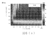
図6(a)と図6(b)は、図6(a)のように堆積し、又は図6(b)のようにレーザー溶融急冷の代表的な組成物のためのレーザパワーと持続時間との関数としての反射率変化を示す。図6(b)に示すように、40ns/40mWでのレーザーパルスは、結晶セット状態から非結晶リセット状態への変化を生成するために十分である。このような40nsのパルス時間は、約30nsのパルス時間と比較できて、結晶セット状態から非結晶リセット状態にGST−225族から材料を変化するためのものである。 FIGS. 6 (a) and 6 (b) show the laser power and duration for a typical composition deposited as shown in FIG. 6 (a) or laser melt quenched as shown in FIG. 6 (b). The reflectance change as a function of. As shown in FIG. 6B, the laser pulse at 40 ns / 40 mW is sufficient to generate a change from the crystal set state to the amorphous reset state. Such a pulse time of 40 ns can be compared with a pulse time of about 30 ns, and is for changing the material from the GST-225 group from the crystal set state to the amorphous reset state.
図7(a)は、結晶セット状態からの約42.9%のGe原子パーセント濃度、20.5%のSb原子パーセント濃度、及び36.6%のTe原子パーセント濃度を有する代表的な組成物のサンプルの非結晶化製図を示す。図7(b)は、消去仕事率の関数としての代表的な組成物の材料のサンプルの結晶化断片を示す。消去仕事率は、書き込み条件に直接関連していることは明らかである。GST−212族内の材料の結晶化は、GST−225族内の材料に観察されるではなく、成長支配変化プロセスよりも核成長支配変化プロセスを介して行われることを示す。GST−212族内の材料の結晶化は、核成長支配変化プロセスよりも成長支配変化プロセスを介して行われると、材料内の欠陥が存在し、容易に結晶化を促進していない。したがって、GST−212族の材料は、欠陥が存在する時、GST−225族からの材料のように低い温度で結晶化することができない。 FIG. 7 (a) shows a representative composition having a Ge atomic percent concentration of about 42.9%, a Sb atomic percent concentration of 20.5%, and a Te atomic percent concentration of 36.6% from the crystal set state. A non-crystallizing draft of the sample is shown. FIG. 7 (b) shows a crystallized fragment of a sample of a representative composition material as a function of erase power. Obviously, the erasing power is directly related to the writing condition. It is shown that crystallization of materials within the GST-212 group is not observed in materials within the GST-225 group, but is performed through a nuclear growth-dominated change process rather than a growth-dominated change process. When crystallization of a material in the GST-212 group is performed through a growth-dominated change process rather than a nuclear growth-dominated change process, defects in the material exist and the crystallization is not easily promoted. Therefore, GST-212 group materials cannot crystallize at low temperatures like defects from GST-225 group when defects are present.
GST−212族内の材料を非結晶リセット状態から結晶セット状態に変化させるために必要な時間も、セット速度として知られており、GST−225族内の材料のためのセット速度に似ている。図8は、約42.9%のGe原子パーセント濃度、約20.5%のSb原子パーセント濃度及び約36.6%のTe原子パーセント濃度を有する代表的な組成物から製造された相変化メモリ装置のR−I曲線を示す。 The time required to change the material in the GST-212 group from the amorphous reset state to the crystalline set state is also known as the set speed, which is similar to the set speed for materials in the GST-225 group. . FIG. 8 shows a phase change memory fabricated from a representative composition having a Ge atomic percent concentration of about 42.9%, a Sb atomic percent concentration of about 20.5%, and a Te atomic percent concentration of about 36.6%. The R-I curve of the device is shown.
図8でのテストされたメモリセルは、30nmから50nmまでの第一電極を有している。図8に示すように、抵抗は、80nsのセットパルス電流を用いて、106と107Ωとの間の非結晶リセット状態の抵抗から、105Ω以下の結晶セット状態の抵抗に落とす。このセットパルス電流の時間は、図9にさらに示され、図9は、セット速度の関数としての結晶セット状態の抵抗のシュムプロット(Shmoo plot)である。図9でのデータを生成するためにテストされたメモリセルは、図8のデータを生成するために使用された前述のメモリセルと同じである。図9から明らかなように、80nsのセット速度を用いて、100kΩの結晶セット状態の抵抗が達成される。GeリッチなGST−212族内の材料の80nsのセット速度は、GST−225族内の材料から製造された装置でセット速度に比較できる。従って、GST−212族の材料を形成するようにGeを加えると、より高い温度でメモリセルのパフォーマンスを向上させ、且つ高いセット速度を維持する。このような高いセット速度は、GST−225族における材料から製造されたメモリセルの有益な特徴である。 The tested memory cell in FIG. 8 has a first electrode from 30 nm to 50 nm. As shown in FIG. 8, the resistance is dropped from a resistance in the amorphous reset state between 106 and 107Ω to a resistance in the crystal set state of 105Ω or less using a set pulse current of 80 ns. The time of this set pulse current is further shown in FIG. 9, which is a Shmoo plot of the resistance of the crystal set state as a function of the set speed. The memory cells tested to generate the data in FIG. 9 are the same as the previously described memory cells used to generate the data in FIG. As is apparent from FIG. 9, a crystal set state resistance of 100 kΩ is achieved using a set speed of 80 ns. The 80 ns set speed of materials within the Ge-rich GST-212 group can be compared to the set speed with equipment manufactured from materials within the GST-225 group. Thus, the addition of Ge to form a GST-212 material improves memory cell performance at higher temperatures and maintains a high set speed. Such a high set speed is a beneficial feature of memory cells fabricated from materials in the GST-225 family.
図10は、GST−212族とGST−225族の両方の様々な材料のためのセットパルスの時間関数としてのセット抵抗のグラフである。図10のデータを生成するために使用されるメモリセルは、図8と図9のデータを生成するために使用される前述装置と同じである。図10は、80nsのセット速度を用いて、結晶セット状態の抵抗が達成されることを示す。図10に示すように、105Ω以下のセット結晶状態の抵抗を達成するために、GST−212の材料に使用されたセットパルス時間の長さを用いて、GST−225のセット結晶状態の抵抗に使用されたセットパルス時間に比較し得る。これは、上昇温度での装置のパフォーマンス特性が改善されている時、所望の高いセットパルス時間はまだ保存されていることを更に示す。 FIG. 10 is a graph of set resistance as a function of set pulse time for various materials in both GST-212 and GST-225. The memory cells used to generate the data of FIG. 10 are the same as the previously described devices used to generate the data of FIGS. FIG. 10 shows that the resistance of the crystal set state is achieved using a set speed of 80 ns. As shown in FIG. 10, the set crystal state resistance of GST-225 is used to achieve the set crystal state resistance of 105Ω or less, using the length of the set pulse time used for the GST-212 material. It can be compared to the set pulse time used. This further indicates that the desired high set pulse time is still preserved when the performance characteristics of the device at elevated temperatures are improved.
GST−212族内の材料は、GST−225がドープされていないものよりもわずかに高い抵抗ドリフト係数を有する。図11は、セット状態とリセット状態との間のメモリセルを変化させる各サイクルの関数としての結晶セット状態と非晶質リセット状態の両方のセル抵抗を示す。図11のデータを生成するために使用されるテストメモリセルは、図8と図9のデータを生成するために使用される構造と同じである。さらに、このようなメモリセルは、GST−212族内で最適なパフォーマンス特性材料から製造されている。図11に示すように、GST−212族内の材料の抵抗ドリフト係数は0.102である。この抵抗ドリフト係数は、ドープされていないGST−225族内の材料の典型的な抵抗ドリフト係数よりもわずかに0.096くらい高くなる。したがって、通常の操作温度で、GST−212族内の材料から製造されるメモリセルは、多数の操作サイクルの間に、セットとリセット状態の両方の抵抗値を大幅に変化させていない。そのような望ましいパフォーマンス特性は、ドープされていないGST−225族内の材料から製造されるメモリセルにおいて観察される多数の操作サイクルの間に、セットとリセット状態の抵抗値の変化不足の特性に似ている。 Materials within the GST-212 group have a slightly higher resistance drift coefficient than those not doped with GST-225. FIG. 11 shows the cell resistance of both the crystal set state and the amorphous reset state as a function of each cycle that changes the memory cell between the set state and the reset state. The test memory cell used to generate the data of FIG. 11 is the same as the structure used to generate the data of FIGS. Furthermore, such memory cells are manufactured from optimal performance characteristic materials within the GST-212 family. As shown in FIG. 11, the resistance drift coefficient of the material in the GST-212 group is 0.102. This resistance drift coefficient is only 0.096 higher than the typical resistance drift coefficient for materials in the undoped GST-225 family. Thus, at normal operating temperatures, memory cells manufactured from materials within the GST-212 family do not significantly change both the set and reset state resistance values during multiple operating cycles. Such desirable performance characteristics are due to the poor change in resistance values in the set and reset states during the numerous operating cycles observed in memory cells fabricated from materials in the undoped GST-225 family. It is similar.
図12は、約42.9%のGe原子パーセント濃度、約20.5%のSb原子パーセント濃度及び約36.6%のTe原子パーセント濃度を有する代表的な組成物から製造されたメモリセルのビット数を示す。図12に示されるように、装置のテストの時に、アレイ内の104個のメモリセルは、セット状態の抵抗値を保持し、且つアレイ内の104個以上のメモリセルは、リセット状態の抵抗値を保持する。結晶セット状態の抵抗値の変化は、5kΩと20kΩとの間の狭い範囲に限られている。一方、非結晶リセット状態の抵抗値の変化は、400kΩと2000kΩとの間の狭い範囲に限られている。限定され且つ分離された範囲における抵抗値の狭い分布は、前述の所望のパフォーマンス特性をさらに示し、そこで、セットとリセット状態の抵抗値は、多数の操作サイクルの後、狭い範囲内で、独立を維持し且つ相対的に一定に維持する。 FIG. 12 shows a memory cell fabricated from a representative composition having a Ge atomic percent concentration of about 42.9%, an Sb atomic percent concentration of about 20.5%, and a Te atomic percent concentration of about 36.6%. Indicates the number of bits. As shown in FIG. 12, during testing of the device, 104 memory cells in the array retain a set state resistance value, and 104 or more memory cells in the array have a reset state resistance value. Hold. The change in resistance value in the crystal set state is limited to a narrow range between 5 kΩ and 20 kΩ. On the other hand, the change in resistance value in the amorphous reset state is limited to a narrow range between 400 kΩ and 2000 kΩ. The narrow distribution of resistance values in a limited and isolated range further illustrates the desired performance characteristics described above, where the resistance values in the set and reset states are independent within a narrow range after multiple operating cycles. And maintain relatively constant.
GST−212族内の材料から製造されるメモリセルは、高いデータ保持レベルを維持し、長時間の高温に曝露した後、誤りデータの作成の低いインスタンスがある。図13は、メモリセルが190°Cで長い時間に曝露された後、代表的な組成物から製造されたメモリセルのアレイ用のビット数をリセット状態抵抗値の関数として示す。図13のデータを生成するために使用されるメモリセルは、図8と図9のデータを生成するために使用されたものと同じである。メモリセルは、最大時間が1〜6時間に焼いた。メモリセルは、6時間に焼いた後、わずか1時間焼いたメモリセルと同じなリセット状態の抵抗値を保持した。したがって、GST−212族から製造されたメモリセルは、上昇温度で長い時間に曝露され、繰り返し循環操作中に非結晶リセット状態の抵抗値を維持することが可能である。 Memory cells made from materials within the GST-212 family maintain high data retention levels and have a low instance of error data creation after exposure to high temperatures for extended periods of time. FIG. 13 shows the number of bits for an array of memory cells made from a typical composition as a function of reset state resistance after the memory cells have been exposed to 190 ° C. for a long time. The memory cells used to generate the data of FIG. 13 are the same as those used to generate the data of FIGS. The memory cell was baked to a maximum time of 1-6 hours. After the memory cell was baked for 6 hours, it retained the same reset resistance value as the memory cell baked for only 1 hour. Therefore, memory cells manufactured from the GST-212 family can be exposed to elevated temperatures for a long time and maintain a non-crystalline reset state resistance during repeated cycling operations.
図14は、メモリセルが190°Cで様々な時間に曝露された後、SiO2がドープされたGST−225族内の材料から製造されたメモリセルのアレイ用のビット数をリセット状態抵抗値の関数として示す。SiO2がドープされたGST−225族内の材料から製造されたメモリセルのアレイは、190°Cの温度で1〜6時間に曝露された。図14は、様々な時間に上昇温度で曝露された後、メモリセルアレイの非結晶リセット状態の抵抗を示す。図14から明らかなように、高い非結晶リセット状態の抵抗にあるアレイにおけるメモリセルの数は、190℃の温度でわずか1時間に暴露された後、劇的に低下していた。一方、図13に示すように、GST−212族内の材料から製造されたメモリセル、190℃の温度で6時間に露出された後、2000kΩのように高い維持アモルファスリセット状態の抵抗値に示すように、したがって、GST−212族の材料から製造されたメモリセルは、GST−225族における材料から製造されたメモリセルに対照させ、優れたデータ保持率などの優れた高温パフォーマンス特性を維持する。 FIG. 14 shows the reset state resistance value for the number of bits for an array of memory cells made from materials within the GST-225 group doped with SiO 2 after the memory cells were exposed at 190 ° C. for various times. As a function of An array of memory cells made from materials within the GST-225 group doped with SiO 2 was exposed at a temperature of 190 ° C. for 1-6 hours. FIG. 14 shows the amorphous reset state resistance of the memory cell array after exposure at elevated temperatures for various times. As can be seen from FIG. 14, the number of memory cells in the array in high amorphous reset state resistance dropped dramatically after being exposed to a temperature of 190 ° C. for only 1 hour. On the other hand, as shown in FIG. 13, a memory cell manufactured from a material in the GST-212 group, after being exposed to a temperature of 190 ° C. for 6 hours, shows a resistance value in a maintained amorphous reset state as high as 2000 kΩ. As such, memory cells fabricated from GST-212 family materials maintain superior high temperature performance characteristics such as superior data retention as compared to memory cells fabricated from GST-225 family materials. .
図15は、GST−212材料から製造されるメモリセル300の断面図を示す。メモリセル300は、メモリ素子302を含み、メモリ素子302は、メモリ材料の本体で構成され、そこで、相変化メモリ材料のバルク化学量論は、GST−212族にある。メモリセル300は、活性領域304を含む。メモリセル300は、第一電極306を含み、第一電極306は、誘電体層308を介して延び、メモリ素子302の底面に接触する。第二電極310は、メモリ素子302に形成され、第一電極306と第二電極310との間に、メモリ素子302を介して電流を生成する。第一および第二電極306及び310は、例えば、TiNやTaNを含むことができる。又、第一および第二電極306及び310のそれぞれは、W、WN、TiAlN、又はTaAlNであり、さらなる例としては、ドープされたSi、Si、C、Ge、Ti、W、Mo、Al、Ta、Cu、Pt、Ir、La、Ni、N、O、Ru及びそれらの組み合わせから成る群から選ばれる一つ以上の元素である。誘電体層308は、窒化ケイ素、酸窒化シリコン、シリコン酸化物と他の任意の適切な誘電体材料を含むことができる。
FIG. 15 shows a cross-sectional view of a
説明されたメモリセルは、比較的狭い幅312(いくつかの実施形態では直径である)を有する第一電極306を有している。第一電極306の狭い幅312は、第一電極306とメモリ素子302との間の接触面積がメモリ素子302と第二電極310との間の接触面積よりも小さいという結果が得られる。したがって、電流は、第一電極306に隣接するメモリ素子302の一部に集中して、活性領域304が第一電極306に近づいている又は接触していることが得られる。メモリ素子302は、活性領域304の外側にある不活性領域を含み、不活性領域は、操作中に相転移を起こさないように非活性になる。活性領域304の外側にある不活性領域は、装置の操作中にも相転移を起こさなく、全体のメモリ素子のバルク化学量論は、活性領域304と不活性領域を含み、GST―212の相変化メモリ材料で構成されている。
The described memory cell has a
図16は、別の設計のメモリセル370の断面図を示す。メモリセル370は、メモリ素子372を含み、メモリ素子372は、電極間の電流経路にメモリ素子372を介して、GST−212族からの材料のバルク化学量論を有する相変化材料の本体からなる。メモリ素子372は、柱形状であり、第一及び第二電極374、376のそれぞれの上部及び下部表面378と380と接触している。メモリ素子372は、第一及び第二電極374、376と実質的に同じ幅384を有し、誘電体(図示せず)によって囲まれた多層の柱を定義する。本明細書に使用される用語 "実質的に"は、製造公差に対応するために意味する。操作の期間に、電流が第一と第二電極374、376との間に流れ、且つメモリ素子372を介して貫通し、メモリ素子における活性領域382が他の領域よりも迅速に熱くなる。これにより、装置の操作中に、大部分の相転移は、活性領域内で発生することになる。
FIG. 16 shows a cross-sectional view of another design of
図17は、別の設計のメモリセル400の断面図を示す。メモリセル400は、メモリ素子402を含み、メモリ素子402は、電極間の電流経路にメモリ素子402を介して、GST−212族からの材料のバルク化学量論を有する相変化材料の本体からなる。メモリ素子402は、誘電体(図示せず)によって囲まれ、第一及び第二電極404、406のそれぞれの上部及び下部表面408と410と接触している。メモリ素子402は、可変幅412を有し、常に第一及び第二電極の幅より小さい。操作の期間に、電流が第一と第二電極404、406との間に流れ、且つメモリ素子402を介して貫通し、活性領域414がメモリ素子の残りの部分よりも迅速に熱くなる。従って、活性領域におけるメモリ素子402のボリューム(volume)は、装置の操作中に、大部分の相転移が発生する場所である。
FIG. 17 shows a cross-sectional view of a
当業者が理解するように、GST―212族のメモリ材料は、本明細書に記載のメモリセル構造に限定されず、メモリセル構造のさまざまな用途に使用することができる。 As those skilled in the art will appreciate, the GST-212 family of memory materials is not limited to the memory cell structures described herein, and can be used in a variety of memory cell structure applications.
図18は、スパッタリングシステムを介してGST−212のメモリ装置を製造する方法の概略図である。スパッタリングシステムは、チャンバ320を含み、チャンバ320には、GST−225スパッタリングターゲット322、Geスパッタリングターゲット324及び基板326が取り付けられる。ターゲット322と324及び基板326は、スパッタリングプロセスの期間にバイアス電圧を印加するために使用される電源及びコントローラ328に接続される。バイアス電圧は、DC、パルスDC、無線周波数、及びそれらの組み合わせに適用され、特定のスパッタリングプロセスに適合するように、コントローラによってオンとオフにし且つ変調される。チャンバ320には、チャンバを排気し、廃気ガスを除去するように、真空ポンプ330または他の手段が装備されている。また、チャンバ320には、ガス源332が構成されている。本発明の一実施形態では、ガス源332は、アルゴンなどの不活性ガスの源である。更に、いくつかの実施形態は、反応ガスのガス源332を含み、例えば酸素または窒素などの反応ガスを使用して、大量のGST−212における他の成分を添加する。システムは、スパッタリング工程で形成される層の組成物に影響を与えるように、ガス源332からのガスの流れを動的に制御する能力を有している。電源は、電源装置に適用され、コントローラ328からGeスパッタリングターゲット324までの電源は、堆積層の組成物を制御するように使用することができ、そのため、前記組成物は、GST−212族の材料に属する。
FIG. 18 is a schematic diagram of a method for manufacturing a GST-212 memory device via a sputtering system. The sputtering system includes a
コリメータ(図示せず)は、高いアスペクト比の特徴に対する適用範囲の均一性を向上させるために(及び他の理由のために)、高いアスペクト比の特徴を有する基板をスパッタリングする時に使用することができる。いくつかのスパッタリング装置は、必要に応じて、スパッタリングチャンバにコリメータを出入する性能を有している。 A collimator (not shown) may be used when sputtering a substrate with high aspect ratio features to improve coverage uniformity for high aspect ratio features (and for other reasons). it can. Some sputtering devices have the ability to move the collimator into and out of the sputtering chamber as needed.
本明細書に記載される説明は、発見的目的のために十分な簡略図解であることが理解されるであろう。スパッタリングチャンバは、標準的な半導体製造工場内の機器であり、さまざまな市販ソースから利用可能である。 It will be understood that the description provided herein is a simplified illustration sufficient for heuristic purposes. Sputtering chambers are standard semiconductor manufacturing plant equipment and are available from a variety of commercial sources.
図19は、別のスパッタリングシステムを介してGST−212族内の物質からメモリ装置を製造する方法の概略図である。図19は、図18のスパッタリング装置と異なり、そのスパッタリングターゲット334は、GST−212族の材料で構成され、且つ独立したGeスパッタリングターゲットを利用されていない。したがって、全体のGST−212材料は、GST−212ターゲットから基板上に堆積され、Geターゲットと組み合わせるGST−225ターゲットからのものではない。
FIG. 19 is a schematic diagram of a method for manufacturing a memory device from a material within Group GST-212 via another sputtering system. FIG. 19 differs from the sputtering apparatus of FIG. 18 in that the
図20は、前述方法のいずれかを用いてGST−212相変化材料の層を形成するためのプロセスフローを示す。前記プロセスは、先に、ゲルマニウム(Ge)、GST−225相変化材料ターゲット、又はGST−212族としての材料組成ターゲットを有するスパッタチャンバ内にウエハを取り付ける(350)。次に、チャンバは、ターゲット・ソースやソースからのスパッタイオンの流れの作成を可能にするために排気される(352)。アルゴンなどの不活性ガスは、スパッタリングに適した雰囲気を確立するように、チャンバに流入される(354)。スパッタチャンバ内に電界を確立して、スパッタリングプロセスを誘導する必要があるために、適当なバイアス電圧は、DCバイアスのように、基板とターゲットを介して印加される(356)。必要に応じて、雰囲気にウェハを露出する前に、プレスパッタリングの間隔は、スパッタリングターゲットを準備するように実行することができる。基板上のメモリ材料の所望の厚さを得るように、スパッタリングの条件は、十分な時間間隔でウエハを露出することによって維持される(358)。バイアスがオフになって、チャンバがどっと流される(360)。最後に、堆積したGST−212層を有するウェハまたは基板が除去される(362)。図21は、図15に示すメモリセルの構造を有するメモリ素子を含むメモリセルを製造するための製造プロセスフローを示す。そこで、メモリ素子のバルク化学量論は、GST−212族からの材料である。メモリセルの要素に適用される参照数字は、図15で使用されるものに対応している。ステップ450では、第一電極306は、幅または直径312を有する誘電体層308を介して延びて形成される。第一電極306は、TiNを含み、誘電体層308は、SiNを含む。あるいは、第一電極306は、サブリソグラフィーの幅または直径312を有することができる。
FIG. 20 shows a process flow for forming a layer of GST-212 phase change material using any of the methods described above. The process first attaches a wafer (350) in a sputter chamber having germanium (Ge), a GST-225 phase change material target, or a material composition target as the GST-212 family. The chamber is then evacuated (352) to allow creation of a target source and sputter ion flow from the source. An inert gas, such as argon, is flowed into the chamber to establish a suitable atmosphere for sputtering (354). Due to the need to establish an electric field in the sputter chamber to induce the sputtering process, an appropriate bias voltage is applied (356) through the substrate and target, such as a DC bias. If desired, a pre-sputtering interval can be performed to prepare the sputtering target before exposing the wafer to the atmosphere. Sputtering conditions are maintained by exposing the wafer at sufficient time intervals (358) to obtain the desired thickness of memory material on the substrate. The bias is turned off and the chamber is flushed (360). Finally, the wafer or substrate having the deposited GST-212 layer is removed (362). FIG. 21 shows a manufacturing process flow for manufacturing a memory cell including a memory element having the memory cell structure shown in FIG. Thus, the bulk stoichiometry of the memory element is a material from the GST-212 group. The reference numerals applied to the elements of the memory cell correspond to those used in FIG. In
第一電極306は、誘電体層308を介して下にあるアクセス回路(図示せず)に延びている。下にあるアクセス回路は、当該分野で公知の標準的なプロセスによって形成され、アクセス回路の要素の構成は、アレイ配置における本明細書中に記載のメモリセルに依存して実行される。一般に、アクセス回路は、半導体基板内のトランジスタ、ダイオード、ワード線、ソース線、導電性プラグ、及びドープされた領域などのアクセス装置を含めることができる。
The
第一電極306と誘電体層308は、例えば、”柱下部電極を有する相変化メモリ装置を製造するための方法”と題する2007年6月18日に出願された米国特許出願11/764,678(現在の米国公開2008/0191187)によって開示された方法、材料、プロセスを使用して形成することができ、この出願は、参照により本明細書に組み込まれている。例えば、電極材料の層は、アクセス回路(図示せず)の上面に形成し、標準的なフォトリソグラフィ技術を使用して、電極層上にフォトレジスト層のパターニングに続いて、第一電極306の位置を覆うフォトレジストマスクを形成することができる。次に、第一電極306の位置を覆うサブリソグラフィー寸法を有するマスク構造を形成するために、例えば酸素プラズマに使用して、フォトレジストマスクがトリミングされる。その後、フォトレジストのトリミングされたマスクを用いて、電極材料の層がエッチングされ、サブリソグラフィー直径312を有する第一電極306を形成する。次に、誘電体材料が形成され、誘電体層308を形成するように平坦化される。
The
ステップ452では、相変化素子がGST−212族からの相変化材料のバルク化学量論を有するように形成される。相変化素子は、上述のように、前に述べたスパッタリングシステムのいずれかの方法によって形成される。
In
次に、ステップ454では、第二電極310が形成され、ステップ456では、バックエンドオブライン(BEOL)プロセスは、チップの半導体プロセスの手順を完了するように実行し、図19に示す構造が得られる。BEOLプロセスは、該当分野で公知の標準的なプロセスとすることができ、実行するプロセスは、メモリセルが実行されるチップの構成に依存する。一般的には、BEOLプロセスによって形成される構造は、接点、層間誘電体、及びチップ上の相互接続の各種金属層を含み、前記チップは、周辺回路へのメモリセルを接続する回路を含む。これらのBEOLプロセスは、上昇温度で誘電体材料の堆積を含み、例えば、400℃でSiNを堆積し、又は500℃やそれ以上の温度で高密度プラズマHDP酸化物蒸着が挙げられる。これらのプロセスの結果として、図14に示すように、制御回路及びバイアス回路は、装置上に形成されている。
Next, in
図22は、メモリアレイ502を含む集積回路500の概略ブロック図であり、メモリアレイ502は、メモリセルを有し、前記メモリセルは、GST−212族における材料のバルク化学量論を有する材料から構成されるメモリ素子を有する。ワード線デコーダ504は、読み取り、セット及びリセットモードを有し、メモリアレイ502における行に沿って配置される複数のワード線506と電気的に通信する。ビット線(列)デコーダ508は、アレイ502における相変化メモリセル(図示せず)を読み取り、セット及びリセットをするように、アレイ502内の列に沿って配置される複数のビット線510と電気的に通信する。アドレスは、バス512で、ワード線デコーダとドライバ504及びビット線デコーダ508に提供される。ブロック514内のセンス回路(センスアンプ)とデータ入力(data−in)構造は、電圧および/またはリード、セット、リセットモードのための電流源を含み、データバス516を介してビット線デコーダ508に接続されている。データは、データ入力線518を介して、集積回路500の入力/出力ポートから、または内部や外部にある集積回路500の他のデータソースから、ブロック514内のデータイン構造体に供給される。他の回路520は、集積回路500に含まれ、例えば、汎用プロセッサ、特殊目的の応用回路、またはアレイ502によってサポートされるシステムオンチップ機能を提供するモジュールの組み合わせが挙げられる。データは、データ出力線522を介して、ブロック514内のセンスアンプから、集積回路500の入力/出力ポートに、または、集積回路500の内部や外部の他のデータの宛先に供給される。
FIG. 22 is a schematic block diagram of an
この例で実行されたコントローラ524は、バイアス配置状態マシンを使用して、バイアス配置の応用のためにバイアス回路の電圧と電流源526を制御し、前記バイアス配置の応用は、ワード線とビット線のための読み取り、書き込み、消去、消去検証及びプログラムが電圧および/または電流を検証することを含む。更に、融解/冷却サイクルのバイアス配置が実行される。コントローラ524は、当技術分野で知られているような特殊用途のロジック回路を用いて実行することができる。別の実施形態では、コントローラ524は、汎用プロセッサを備え、前記汎用プロセッサは、装置の操作を制御するコンピュータプログラムを実行するように同じ集積回路上に実行される。更に、他の実施形態では、特殊目的のロジック回路と汎用プロセッサとの組み合わせは、コントローラ524の実行のために利用される。
The
以上の説明によると、当業者であれば本発明の技術思想を逸脱しない範囲で、多様な変更及び修正が可能であることが分かる。従って、本発明の技術的な範囲は、明細書の詳細な説明に記載された内容に限らず、特許請求の範囲によって定めなければならない。
以下に、本願出願の当初の特許請求の範囲に記載された発明を付記する。
[1]GexSbyTezを含む相変化材料であって、
Ge原子濃度xは、30%〜65%の範囲内にあり、Sb原子濃度yは、13%〜27%の範囲内にあり、Te原子濃度zは、20%〜45%の範囲内にあることを特徴とする相変化材料。
[2]前記材料は、170℃以上の結晶化温度を有し、
前記相変化メモリ材料は、500℃以上の温度で立方結晶構造から六方最密構造に変換し、
前記材料は、成長支配機構を通じて結晶化することを特徴とする[1]に記載の相変化材料。
[3]GexSbyTezを含む相変化材料であって、
Ge原子濃度xは、40%〜65%の範囲内にあり、Sb原子濃度yは、13%〜27%の範囲内にあり、Te原子濃度zは、20%〜45%の範囲内にあることを特徴とする相変化材料。
[4]前記材料は、200℃以上の結晶化温度を有し、
前記相変化メモリ材料は、500℃以上の温度で立方結晶構造から六方最密構造に変換し、
前記材料は、成長支配機構を通じて結晶化することを特徴とする[3]に記載の相変化材料。
[5]第一電極及び第二電極と、
前記第一及び第二電極との間の相変化メモリ材料本体と、を備え、
前記相変化メモリ材料本体のバルク化学量論は、30%〜65%の範囲内にあるGe原子濃度と、13%〜27%の範囲内にあるSb原子濃度と、20%〜45%の範囲内にあるTe原子濃度と、を含むことを特徴とする相変化メモリ材料。
[6]前記相変化メモリ材料本体は、170℃以上の結晶化温度を有し、
前記相変化メモリ材料本体は、成長支配機構を通じて結晶化することを特徴とする[5]に記載の相変化メモリ材料。
[7]第一電極及び第二電極と、
前記第一及び第二電極との間の相変化メモリ材料本体と、を備え、
前記相変化メモリ材料本体のバルク化学量論は、40%〜65%の範囲内にあるGe原子濃度と、13%〜27%の範囲内にあるSb原子濃度と、20%〜45%の範囲内にあるTe原子濃度と、を含むことを特徴とする相変化メモリ材料。
[8]前記相変化メモリ材料本体は、200℃以上の結晶化温度を有し、
前記相変化メモリ材料本体は、成長支配機構を通じて結晶化することを特徴とする[7]に記載の相変化材料。
[9]第一電極を形成する工程と、
Ge原子濃度が30%〜65%の範囲内にあり、Sb原子濃度が13%〜27%の範囲内にあり、Te原子濃度が20%〜45%の範囲内にある相変化メモリ材料本体を形成し、前記第一電極と接触工程と、
第二電極を形成し、前記相変化メモリ材料本体と接触工程と、を備えることを特徴とする相変化メモリ装置の製造方法。
[10]前記本体を形成する工程は、GST−225ターゲット及びGeターゲットから同時スパッタリングすることを含み、
前記本体を形成する工程は、GST−212ターゲットからスパッタリングすることを含み、
バイアス電圧は、Geターゲットと基板の間に印加され、前記相変化メモリ材料本体におけるGe濃度を制御するように使用され、
前記第二電極が形成された後、バックエンドオブライン(BEOL)を実行する工程を更に含み、
前記相変化メモリ材料は、40%〜65%の範囲内にあるGe原子濃度を有することを特徴とする[9]に記載の相変化メモリ装置の製造方法。
From the above description, it will be understood by those skilled in the art that various changes and modifications can be made without departing from the technical idea of the present invention. Therefore, the technical scope of the present invention is not limited to the contents described in the detailed description of the specification, but must be defined by the claims.
Hereinafter, the invention described in the scope of claims of the present application will be appended.
[1] A phase change material comprising GexSbyTez,
The Ge atom concentration x is in the range of 30% to 65%, the Sb atom concentration y is in the range of 13% to 27%, and the Te atom concentration z is in the range of 20% to 45%. A phase change material characterized by that.
[2] The material has a crystallization temperature of 170 ° C. or higher,
The phase change memory material converts from a cubic crystal structure to a hexagonal close-packed structure at a temperature of 500 ° C. or higher,
The phase change material according to [1], wherein the material is crystallized through a growth control mechanism.
[3] A phase change material comprising GexSbyTez,
The Ge atom concentration x is in the range of 40% to 65%, the Sb atom concentration y is in the range of 13% to 27%, and the Te atom concentration z is in the range of 20% to 45%. A phase change material characterized by that.
[4] The material has a crystallization temperature of 200 ° C. or higher,
The phase change memory material converts from a cubic crystal structure to a hexagonal close-packed structure at a temperature of 500 ° C. or higher,
The phase change material according to [3], wherein the material is crystallized through a growth control mechanism.
[5] a first electrode and a second electrode;
A phase change memory material body between the first and second electrodes;
The bulk stoichiometry of the phase change memory material body has a Ge atom concentration in the range of 30% to 65%, a Sb atom concentration in the range of 13% to 27%, and a range of 20% to 45%. A phase change memory material, comprising: a Te atom concentration within.
[6] The phase change memory material body has a crystallization temperature of 170 ° C. or higher,
The phase change memory material according to [5], wherein the phase change memory material body is crystallized through a growth control mechanism.
[7] a first electrode and a second electrode;
A phase change memory material body between the first and second electrodes;
The bulk stoichiometry of the phase change memory material body has a Ge atom concentration in the range of 40% to 65%, a Sb atom concentration in the range of 13% to 27%, and a range of 20% to 45%. A phase change memory material, comprising: a Te atom concentration within.
[8] The phase change memory material body has a crystallization temperature of 200 ° C. or higher,
The phase change material according to [7], wherein the phase change memory material body is crystallized through a growth control mechanism.
[9] forming a first electrode;
A phase change memory material body having a Ge atom concentration in the range of 30% to 65%, an Sb atom concentration in the range of 13% to 27%, and a Te atom concentration in the range of 20% to 45%. Forming and contacting the first electrode;
A method of manufacturing a phase change memory device, comprising: forming a second electrode; and providing the phase change memory material main body and a contact step.
[10] The step of forming the body includes co-sputtering from a GST-225 target and a Ge target,
Forming the body includes sputtering from a GST-212 target;
A bias voltage is applied between the Ge target and the substrate and is used to control the Ge concentration in the phase change memory material body;
After the second electrode is formed, the method further includes performing a back end of line (BEOL),
The method of manufacturing a phase change memory device according to [9], wherein the phase change memory material has a Ge atom concentration in a range of 40% to 65%.
102形状
104対応線
120、122、123、124軌跡
128、130、132結晶セット状態
300、370、400メモリセル
302、372、402メモリ素子
304、414活性領域
306、374、404第一電極
308誘電体層
310、376、406第二電極
312、384、412幅
320チャンバ
322GST−225スパッタリングターゲット
324Geスパッタリングターゲット
326基板
328、524コントローラ
330真空ポンプ
332ガス源
334スパッタリングターゲット
378、382、408上部表面
380、410下部表面
500集積回路
502メモリアレイ
504ワード線デコーダ
506ワード線
508ビット線デコーダ
510ビット線
512バス
514ブロック
516データバス
518データ入力線
520他の回路
522データ出力線
526バイアス回路電圧と電流源。
102
Claims (6)
前記第一及び第二電極との間の相変化メモリ材料本体と、
非結晶相から結晶相まで変更するための80ナノ秒以下の持続時間を有するセットパルスを前記相変化メモリ材料に施すコントローラと、を備え、
前記相変化メモリ材料本体のバルク化学量論は、Ge、SbとTeの原子濃度を示す三元系相図において、30%〜42.9%の範囲内にあるGe原子濃度と、13%〜20.5%の範囲内にあるSb原子濃度と、20%〜36.6%の範囲内にあるTe原子濃度とを含み、前記相変化メモリ材料GeSbTeは、前記Ge、SbとTeの原子濃度範囲内に、前記三元系相図におけるGe/Sb2Te3対応線に沿って配置されている、
ことを特徴とする相変化メモリ装置。 A first electrode and a second electrode;
A phase change memory material body between the first and second electrodes;
A controller for applying to the phase change memory material a set pulse having a duration of 80 nanoseconds or less for changing from an amorphous phase to a crystalline phase;
The bulk stoichiometry of the phase change memory material main body is as follows: In a ternary phase diagram showing atomic concentrations of Ge, Sb, and Te , a Ge atomic concentration within a range of 30% to 42.9%, and 13% to The phase change memory material GeSbTe includes an Sb atomic concentration within a range of 20.5% and a Te atomic concentration within a range of 20% to 36.6%, wherein the phase change memory material GeSbTe has an atomic concentration of Ge, Sb and Te. Within the range, arranged along the Ge / Sb 2 Te 3 corresponding line in the ternary phase diagram ,
A phase change memory device.
前記第一及び第二電極との間の相変化メモリ材料本体と、
非結晶相から結晶相まで変更するための80ナノ秒以下の持続時間を有するセットパルスを前記相変化メモリ材料に施すコントローラと、を備え、
前記相変化メモリ材料本体のバルク化学量論は、Ge、SbとTeの原子濃度を示す三元系相図において、40%〜42.9%の範囲内にあるGe原子濃度と、13%〜20.5%の範囲内にあるSb原子濃度と、20%〜36.6%の範囲内にあるTe原子濃度とを含み、前記相変化メモリ材料GeSbTeは、前記Ge、SbとTeの原子濃度範囲内に、前記三元系相図におけるGe/Sb2Te3対応線に沿って配置されている、
ことを特徴とする相変化メモリ装置。 A first electrode and a second electrode;
A phase change memory material body between the first and second electrodes;
A controller for applying to the phase change memory material a set pulse having a duration of 80 nanoseconds or less for changing from an amorphous phase to a crystalline phase;
The bulk stoichiometry of the phase change memory material body is a ternary phase diagram showing atomic concentrations of Ge, Sb and Te , and a Ge atomic concentration in the range of 40% to 42.9%, and 13% to The phase change memory material GeSbTe includes an Sb atomic concentration within a range of 20.5% and a Te atomic concentration within a range of 20% to 36.6%, wherein the phase change memory material GeSbTe has an atomic concentration of Ge, Sb and Te. Within the range, arranged along the Ge / Sb 2 Te 3 corresponding line in the ternary phase diagram ,
A phase change memory device.
Ge、SbとTeの原子濃度を示す三元系相図において、Ge原子濃度が30%〜42.9%の範囲内にあり、Sb原子濃度が13%〜20.5%の範囲内にあり、Te原子濃度が20%〜36.6%の範囲内にあり、前記相変化メモリ材料GeSbTeは、前記Ge、SbとTeの原子濃度範囲内に、前記三元系相図におけるGe/Sb2Te3対応線に沿って配置されている相変化メモリ材料本体を形成し、前記第一電極と接触工程と、
第二電極を形成し、前記相変化メモリ材料本体と接触工程と、
非結晶相から結晶相まで変更するための80ナノ秒以下の持続時間を有するセットパルスを前記相変化メモリ材料に施す工程と、
を備えることを特徴とする相変化メモリ装置の製造方法。 Forming a first electrode;
In the ternary phase diagram showing the atomic concentrations of Ge, Sb and Te, the Ge atomic concentration is in the range of 30% to 42.9%, and the Sb atomic concentration is in the range of 13% to 20.5%. The Te atom concentration is in the range of 20% to 36.6%, and the phase change memory material GeSbTe is within the Ge, Sb, and Te atomic concentration range, and Ge / Sb 2 in the ternary phase diagram. Forming a phase change memory material body disposed along a Te 3 corresponding line, and contacting the first electrode;
Forming a second electrode, and contacting the phase change memory material body;
Applying to the phase change memory material a set pulse having a duration of 80 nanoseconds or less for changing from an amorphous phase to a crystalline phase;
A method of manufacturing a phase change memory device, comprising:
バイアス電圧は、Geターゲットと基板の間に印加され、前記相変化メモリ材料本体におけるGe濃度を制御するように使用され、
前記第二電極が形成された後、バックエンドオブライン(BEOL)を実行する工程を更に含み、
前記相変化メモリ材料は、40%〜42.9%の範囲内にあるGe原子濃度を有することを特徴とする請求項5に記載の相変化メモリ装置の製造方法。 Forming the body comprises co-sputtering from a GST-225 target and a Ge target or sputtering from a GST-212 target;
A bias voltage is applied between the Ge target and the substrate and is used to control the Ge concentration in the phase change memory material body;
After the second electrode is formed, the method further includes performing a back end of line (BEOL),
6. The method of manufacturing a phase change memory device according to claim 5, wherein the phase change memory material has a Ge atom concentration in a range of 40% to 42.9%.
Applications Claiming Priority (4)
| Application Number | Priority Date | Filing Date | Title |
|---|---|---|---|
| US201161500446P | 2011-06-23 | 2011-06-23 | |
| US61/500,446 | 2011-06-23 | ||
| US13/327,595 US8946666B2 (en) | 2011-06-23 | 2011-12-15 | Ge-Rich GST-212 phase change memory materials |
| US13/327,595 | 2011-12-15 |
Publications (2)
| Publication Number | Publication Date |
|---|---|
| JP2013008948A JP2013008948A (en) | 2013-01-10 |
| JP6062155B2 true JP6062155B2 (en) | 2017-01-18 |
Family
ID=47360979
Family Applications (1)
| Application Number | Title | Priority Date | Filing Date |
|---|---|---|---|
| JP2012103247A Active JP6062155B2 (en) | 2011-06-23 | 2012-04-27 | Ge-rich GST-212 phase change material |
Country Status (5)
| Country | Link |
|---|---|
| US (1) | US8946666B2 (en) |
| JP (1) | JP6062155B2 (en) |
| KR (1) | KR101929458B1 (en) |
| CN (1) | CN102891252A (en) |
| TW (1) | TWI459552B (en) |
Families Citing this family (19)
| Publication number | Priority date | Publication date | Assignee | Title |
|---|---|---|---|---|
| US8680499B2 (en) * | 2012-01-23 | 2014-03-25 | Micron Technology, Inc. | Memory cells |
| US8964442B2 (en) | 2013-01-14 | 2015-02-24 | Macronix International Co., Ltd. | Integrated circuit 3D phase change memory array and manufacturing method |
| CN103117087B (en) * | 2013-01-16 | 2015-08-26 | 华中科技大学 | One in short-term with long-time memory part and storage means |
| US9214229B2 (en) | 2013-06-21 | 2015-12-15 | Macronix International Co., Ltd. | Phase change memory material and system for embedded memory applications |
| KR102077641B1 (en) * | 2013-08-06 | 2020-02-14 | 삼성전자주식회사 | Phase-change material layer and method of manufacturing the same |
| US20160125936A1 (en) * | 2014-11-05 | 2016-05-05 | International Business Machines Corporation | Phase change memory with metastable set and reset states |
| KR102304301B1 (en) * | 2014-12-23 | 2021-09-23 | 삼성전자주식회사 | Resistance-change material layer and phase-change memory device including the same |
| US9672906B2 (en) | 2015-06-19 | 2017-06-06 | Macronix International Co., Ltd. | Phase change memory with inter-granular switching |
| US9917252B2 (en) | 2015-06-19 | 2018-03-13 | Macronix International Co., Ltd. | GaSbGe phase change memory materials |
| US10050196B1 (en) | 2017-05-04 | 2018-08-14 | Macronix International Co., Ltd. | Dielectric doped, Sb-rich GST phase change memory |
| US10541271B2 (en) | 2017-10-18 | 2020-01-21 | Macronix International Co., Ltd. | Superlattice-like switching devices |
| US10374009B1 (en) | 2018-07-17 | 2019-08-06 | Macronix International Co., Ltd. | Te-free AsSeGe chalcogenides for selector devices and memory devices using same |
| TWI771597B (en) | 2019-02-22 | 2022-07-21 | 日商東芝記憶體股份有限公司 | Semiconductor storage device |
| US11289540B2 (en) | 2019-10-15 | 2022-03-29 | Macronix International Co., Ltd. | Semiconductor device and memory cell |
| US11195999B2 (en) | 2019-11-13 | 2021-12-07 | International Business Machines Corporation | Phase change material with reduced reset state resistance drift |
| US11121319B2 (en) | 2019-12-11 | 2021-09-14 | International Business Machines Corporation | Phase-change memory with no drift |
| US11158787B2 (en) | 2019-12-17 | 2021-10-26 | Macronix International Co., Ltd. | C—As—Se—Ge ovonic materials for selector devices and memory devices using same |
| US11380843B2 (en) * | 2020-02-13 | 2022-07-05 | International Business Machines Corporation | Phase change memory using multiple stacks of PCM materials |
| US11362276B2 (en) | 2020-03-27 | 2022-06-14 | Macronix International Co., Ltd. | High thermal stability SiOx doped GeSbTe materials suitable for embedded PCM application |
Family Cites Families (56)
| Publication number | Priority date | Publication date | Assignee | Title |
|---|---|---|---|---|
| US4177475A (en) | 1977-10-31 | 1979-12-04 | Burroughs Corporation | High temperature amorphous memory device for an electrically alterable read-only memory |
| US6033535A (en) | 1990-08-28 | 2000-03-07 | Matsushita Electric Industrial Co., Ltd. | Optical information recording disk and method for manufacturing the same |
| US5596522A (en) | 1991-01-18 | 1997-01-21 | Energy Conversion Devices, Inc. | Homogeneous compositions of microcrystalline semiconductor material, semiconductor devices and directly overwritable memory elements fabricated therefrom, and arrays fabricated from the memory elements |
| EP0601068B1 (en) * | 1991-08-19 | 2002-10-16 | Energy Conversion Devices, Inc. | Electrically erasable, directly overwritable, multibit single cell memory elements and arrays fabricated therefrom |
| US5544103A (en) | 1992-03-03 | 1996-08-06 | Xicor, Inc. | Compact page-erasable eeprom non-volatile memory |
| US7935951B2 (en) | 1996-10-28 | 2011-05-03 | Ovonyx, Inc. | Composite chalcogenide materials and devices |
| US6087674A (en) | 1996-10-28 | 2000-07-11 | Energy Conversion Devices, Inc. | Memory element with memory material comprising phase-change material and dielectric material |
| US5825046A (en) | 1996-10-28 | 1998-10-20 | Energy Conversion Devices, Inc. | Composite memory material comprising a mixture of phase-change memory material and dielectric material |
| US5936274A (en) | 1997-07-08 | 1999-08-10 | Micron Technology, Inc. | High density flash memory |
| US6709958B2 (en) | 2001-08-30 | 2004-03-23 | Micron Technology, Inc. | Integrated circuit device and fabrication using metal-doped chalcogenide materials |
| WO2004008535A1 (en) | 2002-07-11 | 2004-01-22 | Matsushita Electric Industrial Co., Ltd. | Nonvolatile memory and its manufacturing method |
| JP3944455B2 (en) | 2003-01-31 | 2007-07-11 | 松下電器産業株式会社 | Semiconductor device and manufacturing method thereof |
| JP2004241535A (en) * | 2003-02-05 | 2004-08-26 | Matsushita Electric Ind Co Ltd | Resistance varying element and method of manufacturing it |
| JP4011523B2 (en) | 2003-07-07 | 2007-11-21 | シャープ株式会社 | Application management device |
| US7893419B2 (en) | 2003-08-04 | 2011-02-22 | Intel Corporation | Processing phase change material to improve programming speed |
| JP2005117030A (en) * | 2003-09-17 | 2005-04-28 | Mitsubishi Materials Corp | Phase-change film for semiconductor nonvolatile memory, and sputtering target for forming the film |
| WO2005031752A1 (en) * | 2003-09-26 | 2005-04-07 | Kanazawa University Technology Licensing Organization Ltd. | Multinary memory and method for recording to phase-change type recording medium for it |
| EP1738359A1 (en) * | 2004-04-15 | 2007-01-03 | Koninklijke Philips Electronics N.V. | Optical master substrate with mask layer and method to manufacture high-density relief structure |
| DE102005025209B4 (en) * | 2004-05-27 | 2011-01-13 | Samsung Electronics Co., Ltd., Suwon | Semiconductor memory device, electronic system and method for manufacturing a semiconductor memory device |
| US9231201B2 (en) * | 2004-06-30 | 2016-01-05 | Nxp B.V. | Electric device with a layer of conductive material contacted by nanowires |
| KR100652378B1 (en) | 2004-09-08 | 2006-12-01 | 삼성전자주식회사 | Sb Precursor and Manufacturing Method of Phase-Change Memory Device using the Same |
| JP2006202823A (en) * | 2005-01-18 | 2006-08-03 | Renesas Technology Corp | Semiconductor memory device and its manufacturing method |
| US7355238B2 (en) | 2004-12-06 | 2008-04-08 | Asahi Glass Company, Limited | Nonvolatile semiconductor memory device having nanoparticles for charge retention |
| JP4848633B2 (en) | 2004-12-14 | 2011-12-28 | ソニー株式会社 | Storage element and storage device |
| KR100682969B1 (en) | 2005-08-04 | 2007-02-15 | 삼성전자주식회사 | Phase changing material, Phase change Random Access Memory comprising the same and methods of manufacturing and operating the same |
| US7973384B2 (en) | 2005-11-02 | 2011-07-05 | Qimonda Ag | Phase change memory cell including multiple phase change material portions |
| WO2007057972A1 (en) * | 2005-11-21 | 2007-05-24 | Renesas Technology Corp. | Semiconductor device |
| KR101330769B1 (en) * | 2005-12-12 | 2013-11-18 | 오보닉스, 아이엔씨. | Chalcogenide devices and materials having reduced germanium or telluruim content |
| US20070171705A1 (en) * | 2005-12-15 | 2007-07-26 | Parkinson Ward D | Writing phase change memories |
| US20070267620A1 (en) | 2006-05-18 | 2007-11-22 | Thomas Happ | Memory cell including doped phase change material |
| KR100782482B1 (en) | 2006-05-19 | 2007-12-05 | 삼성전자주식회사 | Phase change memory cell employing a GeBiTe layer as a phase change material layer, phase change memory device including the same, electronic device including the same and method of fabricating the same |
| US7453081B2 (en) | 2006-07-20 | 2008-11-18 | Qimonda North America Corp. | Phase change memory cell including nanocomposite insulator |
| US7913215B2 (en) | 2006-07-26 | 2011-03-22 | Taiwan Semiconductor Manufacturing Co., Ltd. | Memory macro with irregular edge cells |
| US7501648B2 (en) | 2006-08-16 | 2009-03-10 | International Business Machines Corporation | Phase change materials and associated memory devices |
| US8138028B2 (en) | 2007-02-12 | 2012-03-20 | Macronix International Co., Ltd | Method for manufacturing a phase change memory device with pillar bottom electrode |
| US7969769B2 (en) * | 2007-03-15 | 2011-06-28 | Ovonyx, Inc. | Multi-terminal chalcogenide logic circuits |
| KR100814393B1 (en) | 2007-03-21 | 2008-03-18 | 삼성전자주식회사 | Method of forming phase changeable material layer and method of manufacturing a phase changeable memory device using the same |
| US7732888B2 (en) * | 2007-04-16 | 2010-06-08 | Qimonda Ag | Integrated circuit, method for manufacturing an integrated circuit, memory cell array, memory module, and device |
| US8357920B2 (en) | 2007-04-20 | 2013-01-22 | Nxp B.V. | Electronic component, and a method of manufacturing an electronic component |
| US7679163B2 (en) | 2007-05-14 | 2010-03-16 | Industrial Technology Research Institute | Phase-change memory element |
| US7745807B2 (en) | 2007-07-11 | 2010-06-29 | International Business Machines Corporation | Current constricting phase change memory element structure |
| US7893420B2 (en) | 2007-09-20 | 2011-02-22 | Taiwan Seminconductor Manufacturing Company, Ltd. | Phase change memory with various grain sizes |
| US7800159B2 (en) | 2007-10-24 | 2010-09-21 | Silicon Storage Technology, Inc. | Array of contactless non-volatile memory cells |
| US7800943B2 (en) | 2008-01-18 | 2010-09-21 | Qimonda Ag | Integrated circuit having a memory cell arrangement and method for reading a memory cell state using a plurality of partial readings |
| US20090230375A1 (en) * | 2008-03-17 | 2009-09-17 | Taiwan Semiconductor Manufacturing Company, Ltd. | Phase Change Memory Device |
| US7759770B2 (en) | 2008-06-23 | 2010-07-20 | Qimonda Ag | Integrated circuit including memory element with high speed low current phase change material |
| US7888165B2 (en) * | 2008-08-14 | 2011-02-15 | Micron Technology, Inc. | Methods of forming a phase change material |
| US8124950B2 (en) * | 2008-08-26 | 2012-02-28 | International Business Machines Corporation | Concentric phase change memory element |
| US7834342B2 (en) * | 2008-09-04 | 2010-11-16 | Micron Technology, Inc. | Phase change material and methods of forming the phase change material |
| JP4635236B2 (en) * | 2008-10-30 | 2011-02-23 | 独立行政法人産業技術総合研究所 | Manufacturing method of solid-state memory |
| JP2010183017A (en) * | 2009-02-09 | 2010-08-19 | National Institute Of Advanced Industrial Science & Technology | Solid-state memory |
| JP2010287744A (en) * | 2009-06-11 | 2010-12-24 | Elpida Memory Inc | Solid-state memory, data processing system, and data processing apparatus |
| US8363463B2 (en) | 2009-06-25 | 2013-01-29 | Macronix International Co., Ltd. | Phase change memory having one or more non-constant doping profiles |
| US20110049456A1 (en) | 2009-09-03 | 2011-03-03 | Macronix International Co., Ltd. | Phase change structure with composite doping for phase change memory |
| US8685291B2 (en) * | 2009-10-13 | 2014-04-01 | Ovonyx, Inc. | Variable resistance materials with superior data retention characteristics |
| JP5883217B2 (en) | 2009-11-06 | 2016-03-09 | Tdk株式会社 | Hexagonal barium titanate powder, method for producing the same, dielectric ceramic composition, and electronic component |
-
2011
- 2011-12-15 US US13/327,595 patent/US8946666B2/en active Active
-
2012
- 2012-04-17 CN CN2012101121273A patent/CN102891252A/en active Pending
- 2012-04-27 JP JP2012103247A patent/JP6062155B2/en active Active
- 2012-05-09 TW TW101116433A patent/TWI459552B/en active
- 2012-05-10 KR KR1020120049773A patent/KR101929458B1/en active IP Right Grant
Also Published As
| Publication number | Publication date |
|---|---|
| US20120326111A1 (en) | 2012-12-27 |
| JP2013008948A (en) | 2013-01-10 |
| TW201301507A (en) | 2013-01-01 |
| CN102891252A (en) | 2013-01-23 |
| KR101929458B1 (en) | 2018-12-14 |
| US8946666B2 (en) | 2015-02-03 |
| KR20130007416A (en) | 2013-01-18 |
| TWI459552B (en) | 2014-11-01 |
Similar Documents
| Publication | Publication Date | Title |
|---|---|---|
| JP6062155B2 (en) | Ge-rich GST-212 phase change material | |
| US7569844B2 (en) | Memory cell sidewall contacting side electrode | |
| US8324605B2 (en) | Dielectric mesh isolated phase change structure for phase change memory | |
| JP5845083B2 (en) | Sputtering of composite targets to form doped phase change materials | |
| US8158965B2 (en) | Heating center PCRAM structure and methods for making | |
| US8363463B2 (en) | Phase change memory having one or more non-constant doping profiles | |
| US7879645B2 (en) | Fill-in etching free pore device | |
| US7696503B2 (en) | Multi-level memory cell having phase change element and asymmetrical thermal boundary | |
| US9917252B2 (en) | GaSbGe phase change memory materials | |
| US20110049456A1 (en) | Phase change structure with composite doping for phase change memory | |
| TWI442518B (en) | Self aligning pillar memory cell device and method for making the same | |
| US20080173931A1 (en) | Multilevel-Cell Memory Structures Employing Multi-Memory Layers with Tungsten Oxides and Manufacturing Method | |
| TWI421348B (en) | Quaternary gallium tellurium antimony (m-gatesb) based phase change memory devices | |
| US20080096344A1 (en) | Method for Manufacturing a Resistor Random Access Memory with a Self-Aligned Air Gap insulator | |
| US7956344B2 (en) | Memory cell with memory element contacting ring-shaped upper end of bottom electrode | |
| CN108807453B (en) | Dielectric doped and antimony rich GST phase change memory | |
| US8916414B2 (en) | Method for making memory cell by melting phase change material in confined space | |
| TWI400798B (en) | Dielectric-sandwiched pillar memory device | |
| TW202131454A (en) | Memory device and integrated circuit | |
| TW200832679A (en) | Multilevel-cell memory structures employing multi-memory layers with tungsten oxides and manufacturing method |
Legal Events
| Date | Code | Title | Description |
|---|---|---|---|
| A621 | Written request for application examination |
Free format text: JAPANESE INTERMEDIATE CODE: A621 Effective date: 20150320 |
|
| A977 | Report on retrieval |
Free format text: JAPANESE INTERMEDIATE CODE: A971007 Effective date: 20151126 |
|
| A131 | Notification of reasons for refusal |
Free format text: JAPANESE INTERMEDIATE CODE: A131 Effective date: 20151208 |
|
| A521 | Request for written amendment filed |
Free format text: JAPANESE INTERMEDIATE CODE: A523 Effective date: 20160308 |
|
| A131 | Notification of reasons for refusal |
Free format text: JAPANESE INTERMEDIATE CODE: A131 Effective date: 20160614 |
|
| A521 | Request for written amendment filed |
Free format text: JAPANESE INTERMEDIATE CODE: A523 Effective date: 20160914 |
|
| TRDD | Decision of grant or rejection written | ||
| A01 | Written decision to grant a patent or to grant a registration (utility model) |
Free format text: JAPANESE INTERMEDIATE CODE: A01 Effective date: 20161115 |
|
| A61 | First payment of annual fees (during grant procedure) |
Free format text: JAPANESE INTERMEDIATE CODE: A61 Effective date: 20161214 |
|
| R150 | Certificate of patent or registration of utility model |
Ref document number: 6062155 Country of ref document: JP Free format text: JAPANESE INTERMEDIATE CODE: R150 |
|
| R250 | Receipt of annual fees |
Free format text: JAPANESE INTERMEDIATE CODE: R250 |
|
| R250 | Receipt of annual fees |
Free format text: JAPANESE INTERMEDIATE CODE: R250 |
|
| R250 | Receipt of annual fees |
Free format text: JAPANESE INTERMEDIATE CODE: R250 |
|
| R250 | Receipt of annual fees |
Free format text: JAPANESE INTERMEDIATE CODE: R250 |
|
| R250 | Receipt of annual fees |
Free format text: JAPANESE INTERMEDIATE CODE: R250 |